

Page 1
S amHop Microelectronics C orp.
S DP /B65N03L
S eptember , 2002
4
PR ODUC T S UMMAR Y
VDS S
30V
ID
65A
D
G
S
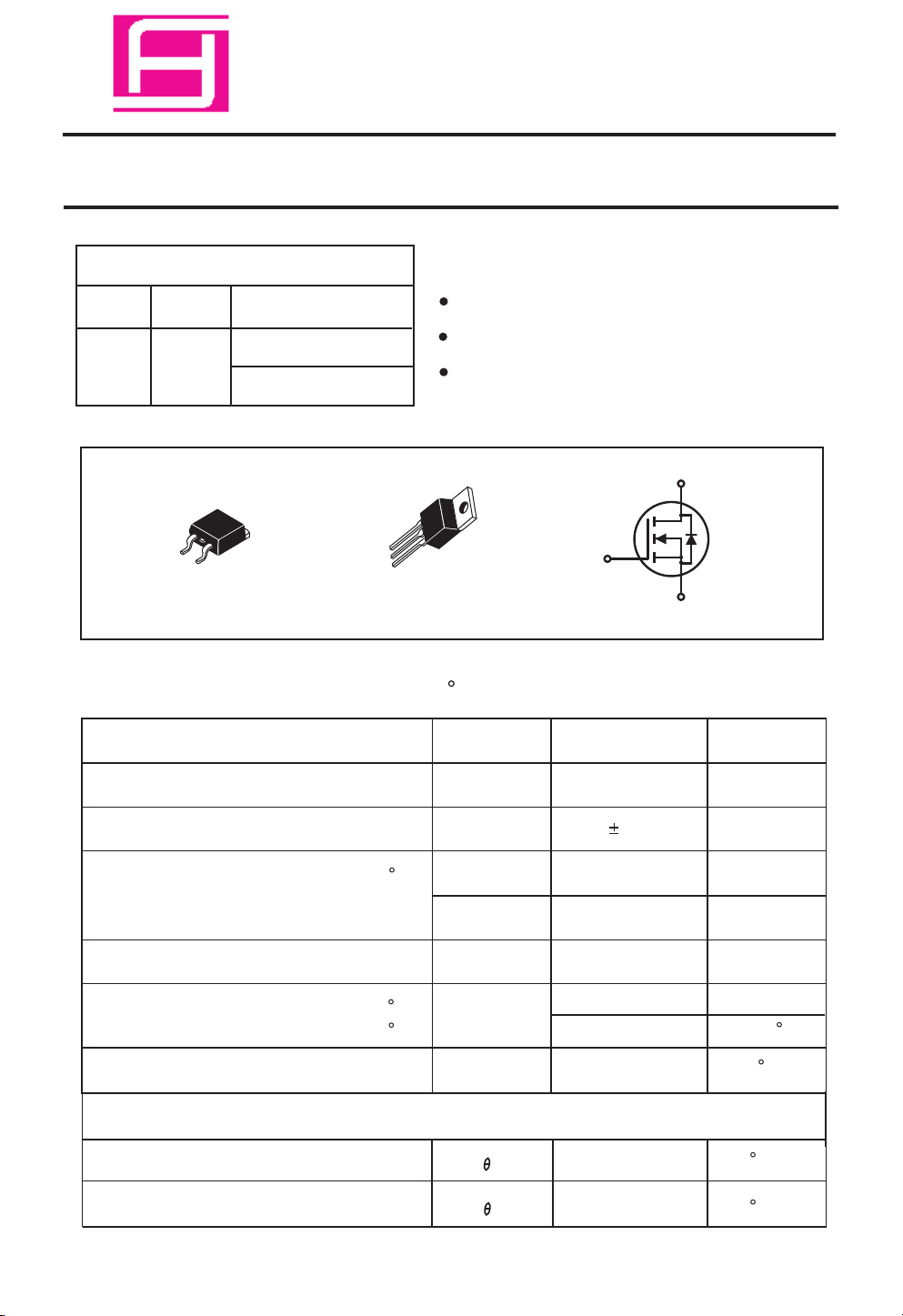
S DB S E RIE S
TO-2 63(DD-PAK)
R DS (on) ( m
12 @ VGS = 4. 5V
W
) T YP
8 @ VGS = 10V
G
D
S
S DP S E RIE S
TO-2 20
F E ATUR E S
S uper high dense cell design for extremely low R DS (ON).
High power and current handling capability.
TO-220 & TO-263 package.
D
G
S
ABS OLUTE MAX IMUM R ATING S (TC =25 C unless otherwise noted)
P arameter
Drain-S ource Voltage
S ymbol
V
DS
Limit Unit
30
V
G ate-S ource Voltage
Drain C urrent-C ontinuous @ TJ =125 C
-P ulsed
a
Drain-S ource Diode Forward C urrent
Maximum P ower Dissipation
@ T c=25 C
Derate above 25 C
Operating and S torage
Temperature R ange
THE R MAL C HAR AC TE R IS TIC S
Thermal R es is tance, J unction-to-C a s e
Thermal R es is tance, J unction-to-Ambient
V
I
P
TJ, T
R
R
G S
I
D
DM
I
S
D
1
S TG
J C
J A
20
65
195
65
75
0.5
-65 to 175
2
62.5
V
A
A
A
W
W / C
C
C
/W
C
/W
Page 2
S DP /B 65N03L
E LE C T R IC AL C H AR AC T E R IS T IC S (T C 25 C unless otherwis e noted)
P arameter
S ymbol
=
C ondition
Min
Typ
OF F CHAR ACT E R IS T IC S
Drain-S ource B reakdown Volta ge
Zero G ate Voltage Drain Current
G a te-Body Leakage
ON C HAR AC TE R IS TIC S
a
G a te T hres hold Voltage
Drain-S ource On-S tate R es istance
On-S ta te Drain C urrent
0V, ID 250uA
B V
DS S
I
DS S
I
G S S
V
G S (th)
R
DS (ON)
I
D(ON)
g
F S
b
VDS 24V, V
V
G S
V
DS VG S
V
G S =
V
G S =
V
DS
V
DS =
=
=
G S
= =
=
=
0V
20V, VDS 0V
=
, ID = 250uA
10V, ID = 26A
4.5V, ID = 21A
= 10V, V
G S
= 10V
10V, ID = 26A
30
1 1.5 3
65
8
12
38
V
G S
DYNAMIC C HAR AC TE R IS TICS
C
Max
10
100
9
15
Unit
V
uA
nA
V
m ohm
m ohm
A
SF orward Transconductance
4
Input C apacitance
Output C apacitance
R evers e Transfer C apacitance
S WIT C HING C HAR AC TE R IS TIC S
Turn-O n Delay Time
R ise Time
Turn-O ff Delay Time
F all Time
Total G ate Charge
G a te-S ource C harge
G a te-Drain C harge
b
C
IS S
C
OS S
C
R S S
t
D(ON)
t
t
D(OFF)
t
Q
Q
Q
V
f =1.0MH
VDD = 15V,
r
ID = 1A,
V
R
f
VDS =10V, ID =65A,V
g
VDS =10V, ID =65A,V
gs
gd
VDS =10V, ID = 65A,
V
DS
=15V, V
G S
= 10V
G E N
G S
=10V
2
= 6
G S
Z
ohm
= 0V
G S
G S
=10V
=4.5V
1350
625
190
30
32
132
30
50
41
20.5 24.5
6.9
5.8
P
F
P
F
P
F
ns
ns
ns
ns
nC
nC
nC
nC
Page 3

S DP /B 65N03L
E LE C T R IC AL C H AR AC T E R IS T IC S (TC=25 C unless otherwis e noted)
4
Typ
P arameter
S ymbol
C ondition
Min
Max
Unit
DR AIN-S O UR C E DIODE C HAR AC T E R IS T IC S
Diode F orward Voltage
Notes
a.Puls e Tes t:P ulse W idth 300us, Duty C ycle 2% .
b.Guaranteed by des ign, not s ubject to production tes ting.
80
70
60
50
40
30
20
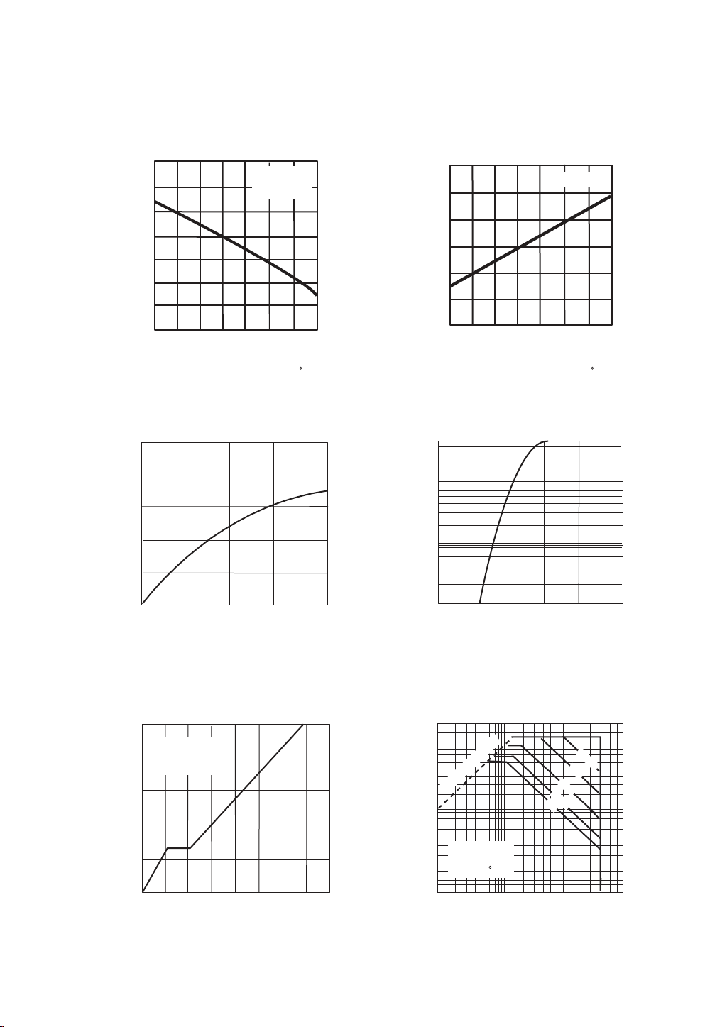
ID, Drain C urrent(A)
10
0
0 0. 5 1. 0 1. 5 2. 0 2.5 3. 0
VDS , Drain-to-S ource Volta ge (V)
F igure 1. O utput C haracteristics
VGS =10, 9,8, 7,6, 5V
V
S D
VGS =4V
VGS =3V
a
V
G S
= 0V, Is =26A
25
20
15
10
ID, Dra in C urrent (A)
1.3
0.9
25 C
5
0
1 2 3 4 5 6
VGS , G ate-to-S ource Volta ge (V)
T J=125 C
-55 C
F igure 2. Trans fer C haracteris tics
V
360 0
300 0
240 0
180 0
120 0
600
C , C apa citanc e (pF)
0
0 5 10 15 20 25 30
VDS , Drain-to S ource V olta ge (V)
F igure 3. C apacitance
C iss
C oss
C rss
2. 2
VGS=10V
I
D
=26A
1. 8
1. 4
1. 0
0. 6
0. 2
Dra in-S ource O n-R es istanc e
R DS (O N), Norma lized
0
-50 0 50 100 125
-25 25
75
F igure 4. O n-R esis tance Variation with
Temperature
3
T j( C)
Page 4
S DP /B 65N03L
1.3
VDS=V
1.2
1.1
1.0
0.9
0.8
Vth, Norma lized
0.7
G ate-Source T hres hold V oltage
0.6
-50 -25 0 25 50 75 100 125
G S
ID=250uA
B VDS S, N ormalized
Tj, J unction T emperature ( C)
1.15
1.10
1.05
1.00
0.95
0.90
0.85
Dra in-S ource Breakdown V oltage
-50 -25 0 2 5 50 75 100 125
ID=250uA
4
Tj, J unction T emperature ( C)
F igure 6. B reakdown V oltage V ariation F igure 5. G ate Thres hold Variation
with T empera ture
50
40
30
20
10
gFS , T rans conductanc e (S )
0
0 10 20 3 0 4 0
VDS=10V
Is , S ource-dra in current (A)
with T empera ture
50
10
1.0
0.1
0.4 0.6 0.8 1.0 1.2 1.4
IDS , Drain-S ource C urrent (A)
F igure 7. T rans conductance Variation
with Drain C urrent
10
8
6
VGS , G ate to S ource Volta ge (V )
0
VDS=10V
ID=65A
4
2
0 6 12 18 3024 36 42 48
Qg, T otal Gate Charge (nC )
F igure 9. G ate C harge
VS D, Body Diode F orward V olta ge (V )
F igure 8. B ody Diode Forward Voltage
Variation with S ource C urrent
300
200
100
10
ID, Dra in C urrent (A )
1
0.5
0.1
mit
i
ON)L
(
S
D
R
V
G S
=10V
S ingle P ulse
Tc=25 C
1
0
ms
1
0
0
ms
DC
1 10 30 60
VDS , Drain-S ource V oltage (V )
F igure 10. Maximum S afe
O perating Area
4
1
0
0
μ
s
1ms
Page 5
S DP /B 65N03L
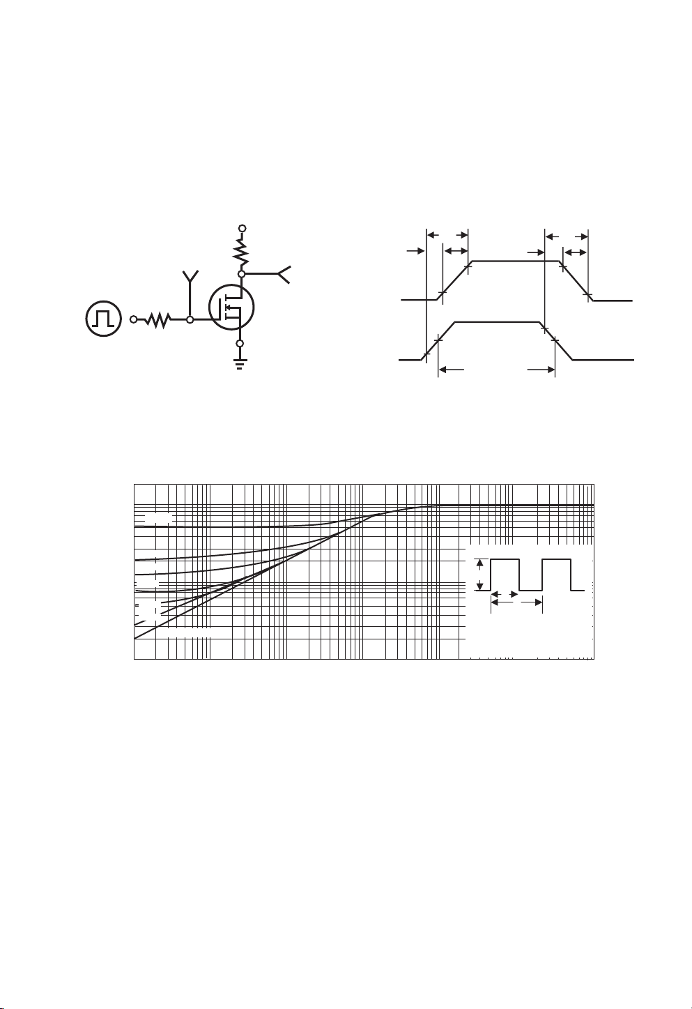
4
IN
V
V
G S
G EN
R
G
DD
V
on
t
d(off)
t
r
t
90%
INVE R TE D
10% 10%
50% 50%
V
V
d(on)
t
OU T
IN
10%
R
L
D
OU T
V
S
90%
t
off
f
t
90%
P ULS E W IDT H
F igure 11. S witching T est C ircuit
2
1
D=0. 5
0. 2
0. 1
0. 1
0. 05
0. 02
r(t), Norma lized Effective
0. 01
T rans ient Thermal Impedance
0. 01
S ingle P ulse
0. 01 0. 1 1 10 100 100 0 100 00
F igure 12. S witching W aveforms
DM
P
1
t
2
t
1. R θJC (t)=r (t) * R θJ C
2. R θJC =S ee D atas heet
3. TJ M-T C = P* R θJC (t)
4. Duty C ycle , D=t1/t2
S quare Wave P ulse Duration (ms ec)
F igure 13. Norma lized T hermal T rans ient Impedance C urve
5
 Loading...