

Page 1

PRELIMINARY DATA SHEET
SDA 9488X PIP IV Basic
SDA 9588X OCTOPUS
Cost-effective
Picture-In-Picture IC s
Edition Feb. 28, 2001
6251-561-1PD
Page 2
SDA 9488X
Preliminary Data Sheet
SDA 9588X
Cost effective Picture-In-Picture (PIP) ICs
Version 1.3 CMOS
General Description
SDA 9488X ’PIP IV Basic’ and SDA 9588X
’OCTOPUS’ belong to a new generation of costeffective PiP processors that combine high-quality
digital PIP signal processing, digital multistandard
color decoding and AD/DA conversion on a single chip.
Both devices are equipped with CVBS and Y/C input
interfaces. In addition the SDA 9588X is also able to
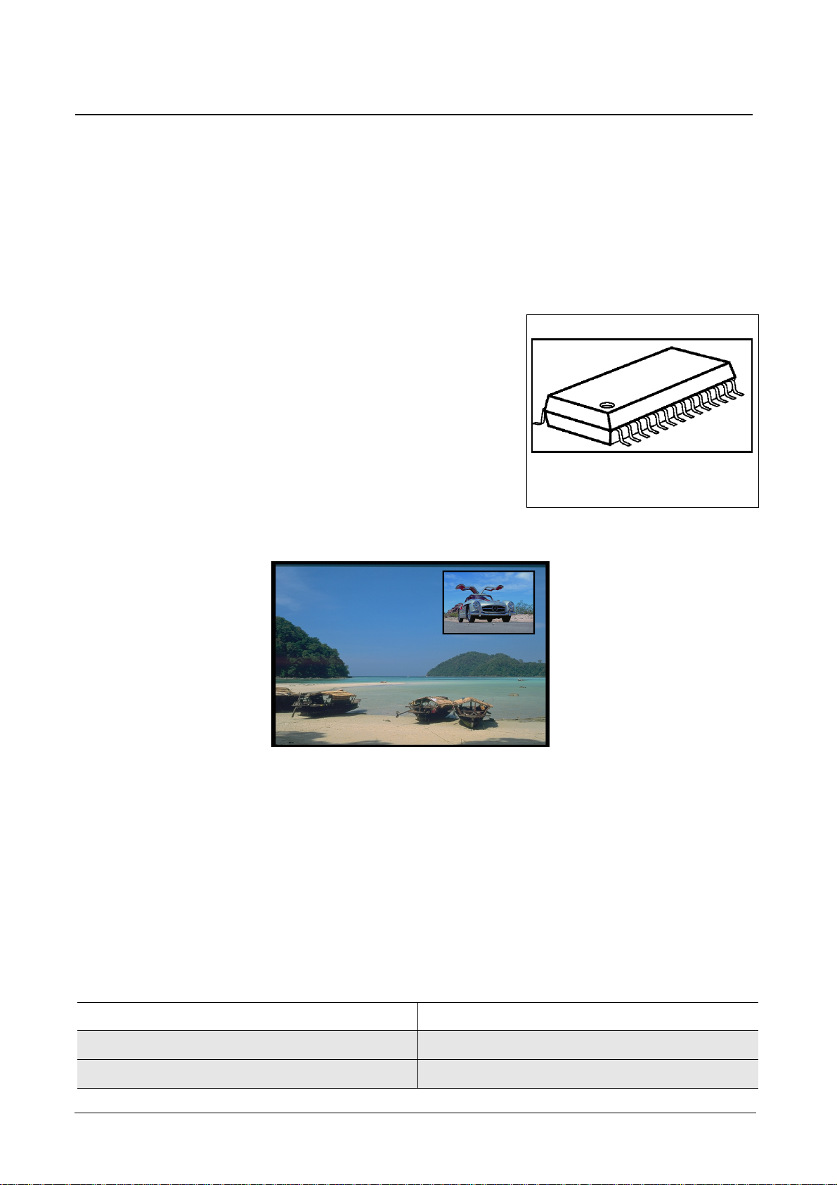
P-DSO28-1
process YUV input signals for displaying high-quality
video signals e.g. coming from a DVD source.
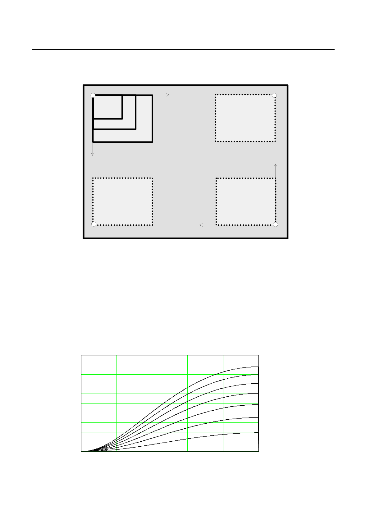
Figure 0-1 Picture-In-Picture
The integrated digital color decoder is able to decode all analog TV standards (PAL,
NTSC and SECAM) and detects the standard automatically. Therefore the IC is suited
for world-wide use.
A picture reduction from 1/9 to 1/81 of original size selectable in fine steps is possible.
The transfer functions of the decimation filters are optimally matched to the selected
picture size reduction and can furthermore be adjusted to the viewer’s requirements by
a selectable peaking. A maximum of 216 luminance and 2x54 chrominance pixels per
line are stored in the memory.
Type Package
SDA 9488X P-DSO28-1
SDA 9588X P-DSO28-1
Micronas -2
Page 3

SDA 9488X
Preliminary Data Sheet
SDA 9588X
1 Features . . . . . . . . . . . . . . . . . . . . . . . . . . . . . . . . . . . . . . . . . . . . . . . . . . . .5
2 Pin Configuration . . . . . . . . . . . . . . . . . . . . . . . . . . . . . . . . . . . . . . . . . . . . .7
3 Block Diagram . . . . . . . . . . . . . . . . . . . . . . . . . . . . . . . . . . . . . . . . . . . . . . .9
4 System Description . . . . . . . . . . . . . . . . . . . . . . . . . . . . . . . . . . . . . . . . . .10
4.1 Analog Frontend . . . . . . . . . . . . . . . . . . . . . . . . . . . . . . . . . . . . . . . . . . . . .10
4.1.1 Input Selection . . . . . . . . . . . . . . . . . . . . . . . . . . . . . . . . . . . . . . . . . . . . .10
4.1.2 AD-Conversion . . . . . . . . . . . . . . . . . . . . . . . . . . . . . . . . . . . . . . . . . . . .10
4.1.3 Automatic Gain Control . . . . . . . . . . . . . . . . . . . . . . . . . . . . . . . . . . . . . .11
4.1.4 Signal Magnitudes . . . . . . . . . . . . . . . . . . . . . . . . . . . . . . . . . . . . . . . . . .11
4.2 Inset Synchronization . . . . . . . . . . . . . . . . . . . . . . . . . . . . . . . . . . . . . . . . .13
4.3 Chroma Decoding And Standard Search . . . . . . . . . . . . . . . . . . . . . . . . . .13
4.4 Comb Filtering . . . . . . . . . . . . . . . . . . . . . . . . . . . . . . . . . . . . . . . . . . . . . . .15
4.5 Luminance Processing . . . . . . . . . . . . . . . . . . . . . . . . . . . . . . . . . . . . . . . .15
4.6 Decimation . . . . . . . . . . . . . . . . . . . . . . . . . . . . . . . . . . . . . . . . . . . . . . . . . .16
4.6.1 Single PIP Mode . . . . . . . . . . . . . . . . . . . . . . . . . . . . . . . . . . . . . . . . . . .16
4.6.2 Horizontal And Vertical Fine Positioning . . . . . . . . . . . . . . . . . . . . . . . . .19
4.6.3 Multi Display Mode . . . . . . . . . . . . . . . . . . . . . . . . . . . . . . . . . . . . . . . . .19
4.7 Display Control . . . . . . . . . . . . . . . . . . . . . . . . . . . . . . . . . . . . . . . . . . . . . .20
4.7.1 Mixed Standard Applications And (S)VGA Support . . . . . . . . . . . . . . . . .23
4.7.2 Display standard . . . . . . . . . . . . . . . . . . . . . . . . . . . . . . . . . . . . . . . . . . .24
4.7.3 Picture Positioning . . . . . . . . . . . . . . . . . . . . . . . . . . . . . . . . . . . . . . . . . .25
4.8 Output Signal Processing . . . . . . . . . . . . . . . . . . . . . . . . . . . . . . . . . . . . . .26
4.8.1 Luminance Peaking . . . . . . . . . . . . . . . . . . . . . . . . . . . . . . . . . . . . . . . . .26
4.8.2 RGB Matrix . . . . . . . . . . . . . . . . . . . . . . . . . . . . . . . . . . . . . . . . . . . . . . .27
4.8.3 Framing And Colored Background . . . . . . . . . . . . . . . . . . . . . . . . . . . . .27
4.8.4 16:9 Inset Picture Support . . . . . . . . . . . . . . . . . . . . . . . . . . . . . . . . . . . .28
4.8.5 Parent Clock Generation . . . . . . . . . . . . . . . . . . . . . . . . . . . . . . . . . . . . .29
4.8.6 Select Signal . . . . . . . . . . . . . . . . . . . . . . . . . . . . . . . . . . . . . . . . . . . . . .30
4.9 DA-Conversion And RGB / YUV Switch . . . . . . . . . . . . . . . . . . . . . . . . . . .30
4.9.1 Contrast, Brightness and Peak Level Adjustment . . . . . . . . . . . . . . . . . .32
4.9.2 Pedestal Level Adjustment . . . . . . . . . . . . . . . . . . . . . . . . . . . . . . . . . . .32
4.10 Data Slicer . . . . . . . . . . . . . . . . . . . . . . . . . . . . . . . . . . . . . . . . . . . . . . . . . .33
4.10.1 Closed Caption . . . . . . . . . . . . . . . . . . . . . . . . . . . . . . . . . . . . . . . . . . . .33
4.10.2 Widescreen Signalling (WSS) . . . . . . . . . . . . . . . . . . . . . . . . . . . . . . . . .34
4.10.3 Indication Of New Data . . . . . . . . . . . . . . . . . . . . . . . . . . . . . . . . . . . . . .34
4.10.4 Violence Protection . . . . . . . . . . . . . . . . . . . . . . . . . . . . . . . . . . . . . . . . .35
5 Application Examples . . . . . . . . . . . . . . . . . . . . . . . . . . . . . . . . . . . . . . . .36
6 I2C Bus . . . . . . . . . . . . . . . . . . . . . . . . . . . . . . . . . . . . . . . . . . . . . . . . . . . .37
6.1 I2C Bus Address . . . . . . . . . . . . . . . . . . . . . . . . . . . . . . . . . . . . . . . . . . . . .37
6.2 I2C-Bus Format . . . . . . . . . . . . . . . . . . . . . . . . . . . . . . . . . . . . . . . . . . . . . .37
Micronas -3
Page 4

SDA 9488X
SDA 9588X
6.3 I2C bus Command Table . . . . . . . . . . . . . . . . . . . . . . . . . . . . . . . . . . . . . . . 38
6.4 I2C Bus Command Description . . . . . . . . . . . . . . . . . . . . . . . . . . . . . . . . . .40
7 Pin Description . . . . . . . . . . . . . . . . . . . . . . . . . . . . . . . . . . . . . . . . . . . . .68
8 Absolute Maximum Ratings . . . . . . . . . . . . . . . . . . . . . . . . . . . . . . . . . . .71
9 Recommended Operating Range . . . . . . . . . . . . . . . . . . . . . . . . . . . . . . . 72
10 Characteristics . . . . . . . . . . . . . . . . . . . . . . . . . . . . . . . . . . . . . . . . . . . . . . 76
11 Diagrams . . . . . . . . . . . . . . . . . . . . . . . . . . . . . . . . . . . . . . . . . . . . . . . . . .80
12 Application Circuit . . . . . . . . . . . . . . . . . . . . . . . . . . . . . . . . . . . . . . . . . . .86
Preliminary Data Sheet
Micronas -4
Page 5

SDA 9488X
SDA 9588X
Preliminary Data Sheet
Features
1Features
• Single chip solution:
– AD-conversion for CVBS or Y/C or YUV
1)
, multistandard color decoding, PLL for
synchronization of inset channel, decimation filtering, embedded memory, RGBmatrix, DA-conversion, RGB/YUV switch, data-slicer and clock generation
integrated on chip
• Analog inputs:
– 3x CVBS or 1x CVBS and 1x Y/C or 1xYUV (SDA 9588X) alternatively
– Clamping of each input
– All ADCs with 8 bit amplitude resolution
– Automatic Gain Control (AGC) for Y and CVBS
• Inset Synchronization:
– Multiple time constants for reliable synchronization
– Automatic recognition of 625 lines / 525 lines standard
• Color Decoder:
– PAL-B/G, PAL-M, PAL-N(Argentina), PAL60, NTSC-M, NTSC4.4 and SECAM
– Adjustable color saturation
– Hue control for NTSC
– Automatic Chroma Control (-24 dB ... +6 dB)
– Automatic recognition of chroma standards: different search strategies selectable
– Single crystal for all standards
– IF-characteristic compensation filter
• Decimation:
– PIP sizes between 1/81 and 1/9 adjustable with steps of 2 lines and 4 pixel
– Resolution up to 216 luminance and 2x54 chrominance pixels per inset line
– Horizontal and vertical filtering dependent on picture size
• Display Features:
– 7 bit per pixel stored in memory
– Field and joint-line free frame mode display
– Display on VGA and SVGA screen (f
limited to 40kHz)
H
– 8 different read frequencies for 16:9 compatibility
– Line doubling mode for progressive scan applications
– Freeze picture
– Coarse positioning at 4 corners of the parent picture
– Fine positioning at steps of 4 pixels and 2 lines
• Output signal processing:
–7 Bit DAC
– RGB or YUV switch: insertion of an external source without PIP processing
– Digital interpolation for anti-imaging
1)
available with SDA 9588X only
Micronas 1-5
Page 6

SDA 9488X
SDA 9588X
Preliminary Data Sheet
– Adjustable transient improvement for luma (peaking)
– Contrast, Brightness and Pedestal Level adjustable
– Analog outputs: Y, +(B-Y), +(R-Y), or Y, -(B-Y), -(R-Y) or RGB
– Three RGB matrices available: NTSC(Japan), NTSC(USA) or EBU
– 64 different background colors and 4096 different frame colors
– Plain or 3D frame with variable width and height
• Data Slicing:
– Slicing of closed-caption (CC) or wide-screen-signaling (WSS) data
– Violence blocking capability (V-chip)
– Several filter for XDS data extraction
2
•I
C-Bus control (400 kHz)
• High stability clock generation
• PDSO 28-1 package (SMD)
• Full SDA 9489X and SDA 9589X upward compatibility
• SDA 9388X / SDA 9389X pinout compatibility
• 3.3V supply voltage (5V input capable)
Features
Micronas 1-6
Page 7
SDA 9488X
SDA 9588X
Preliminary Data Sheet
2 Pin Configuration
XIN
XQ
HSP
VSP
SDA
SCL
VDD
VSS
I2C
INT
IN1
IN2
IN3
FSW
Pin Configuration
1
2
3
4
5
6
7
8
9
10
11
12
13
14
PDSO 28 -1
28
27
26
25
24
23
22
21
20
19
18
17
16
15
CVBS1
VREFM
CVBS2
VREFL
CVBS3
VSSA1
VDDA1
VREFH
VSSA2
VDDA2
OUT1
OUT2
OUT3
SEL
Figure 2-1 Pinning
Figure 2-2 Package Outlines
Micronas 2-7
Page 8
SDA 9488X
SDA 9588X
Preliminary Data Sheet
Numb
er
1 XIN I crystal oscillator (input) or external clock input
2 XQ O crystal oscillator (output)
3 HSP I/TTL horizontal sync for parent channel
4 VSP I/TTL vertical sync for parent channel
5SDAI/OI
6SCL II
7 VDD S digital supply voltage
8 VSS S digital ground
9I2C II
10 INT O/TTL interrupt
11 IN1 I/ana V/R input for external YUV/RGB source
Name Type Description
2
C-bus data
2
C-bus clock
2
C Address
Pin Configuration
12 IN2 I/ana Y/G input for external YUV/RGB source
13 IN3 I/ana U/B input for external YUV/RGB source
14 FSW I fast switch input for YUV/RGB switch
15 SEL O fast blanking output for PIP
16 OUT3 O/ana analog output: chrominance signal +(B-Y) or -(B-Y) or B
17 OUT2 O/ana analog output: luminance signal Y or G
18 OUT1 O/ana analog output: chrominance signal +(R-Y) or -(R-Y) or R
19 VDDA2 S analog supply voltage for DAC
20 VSSA2 S analog ground for DAC
21 VREFH I/ana uppper reference voltage for ADC and DAC
22 VDDA1 S analog supply voltage for ADC
23 VSSA1 S analog ground for ADC
24 CVBS3 I/ana CVBS3 or V (SDA 9588X) or C Input
25 VREFL I/O lower reference voltage for ADC
26 CVBS2 I/ana CVBS2 or U (SDA 9588X) or Y (of Y/C) Input
27 VREFM I/O mid-level reference voltage for ADC
28 CVBS1 I/ana CVBS1 or Y (of YUV, SDA 9588X) Input
I= Input / ana=analog / O= Output / TTL=Digital (TTL) / S=Supply voltage
Table 2-1 Pin Description
Micronas 2-8
Page 9
SDA 9488X
W
3
SDA 9588X
Preliminary Data Sheet
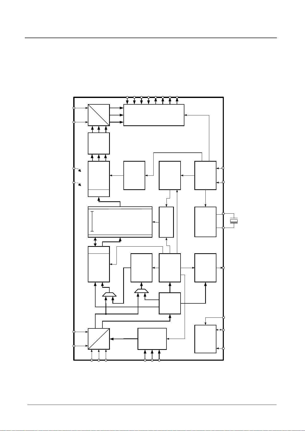
3 Block Diagram
DAC
Triple
VDDA2VSSA2VDD VSS
RGB
8
Over-
Peaking
DEMUX
Block Diagram
IN1
12
11
3x7bit
Matrix
Insertion
sampling
Frame
FS
IN3
IN2
13
Generation
18
14
Fast
RGB/YUV
OUT1OUT2OUT
16
17
Switch
Display
Controller
15
SEL
Parent
Sync
Processing
HSP VSP
MUX
H/V Scaler
Decimation
Skewcomp.
DUV/DCHR
DCVBS/DY
27
ADC
TRIPLE
3x8bit 1)
25
21
22 23 71920
VDDA1 VSSA1
eDRAM
Color
Decoder
Input
28
XTAL
XIN XQI2CSCL SDA
Synthesizer
Acquisition
Controller
1210965 34
20.25 MHz
INTR
1) SDA9588X, SDA 9488X: 2x8bit
512kbit
Memory
Controller
Inset
Sync
Y/C and
Gain
Sync
Processing
Sep.
PAL/ SECAM/ NTSC
Select
Clamp
24
26
Clock
Data Slicer
C
2
I
VREFH
VREFM
VREFL
CVBS1
CVBS2
Figure 3-1 Block Diagram
Micronas 3-9
CVBS3
Page 10
SDA 9488X
SDA 9588X
Preliminary Data Sheet
System Description
4 System Description
4.1 Analog Frontend
4.1.1 Input Selection
An analog inset CVBS signal can be fed to the inputs CVBS1-3 of SDA 9588X resp. SDA
9488X. Each of these sources is selectable via I
2
C bus (CVBSEL). CVBS2 and CVBS3
can be used as separate Y/C inputs. YUV sources can be connected to CVBS1, CVBS2
and CVBS3 provided YUV operation at the SDA 9588X being enabled (YUVSEL). Using
an external switch the SDA 9588X can operate in applications with both YUV and CVBS
signals.
CVBSEL YUVSEL Input remark
D1 D0
CVBS1 CVBS2 CVBS3
0 0 0 CVBS
0 1 0 CVBS
1 0 0 Y (VBS) C Y/C mode
1 1 0 CVBS
X X 1 Y (VBS) U (CB) V (CR) YUV mode
(SDA 9588X only)
Table 4-1 Input selection
4.1.2 AD-Conversion
All signal are clamped and AD-converted with an amplitude resolution of 8bit. CVBS and
Y signals are clamped to the sync bottom whereas U/V and C signals are clamped to
their mid-level during blanking.
Inset
Video
HD
CLMPIST
CLAMPI
CLMPID
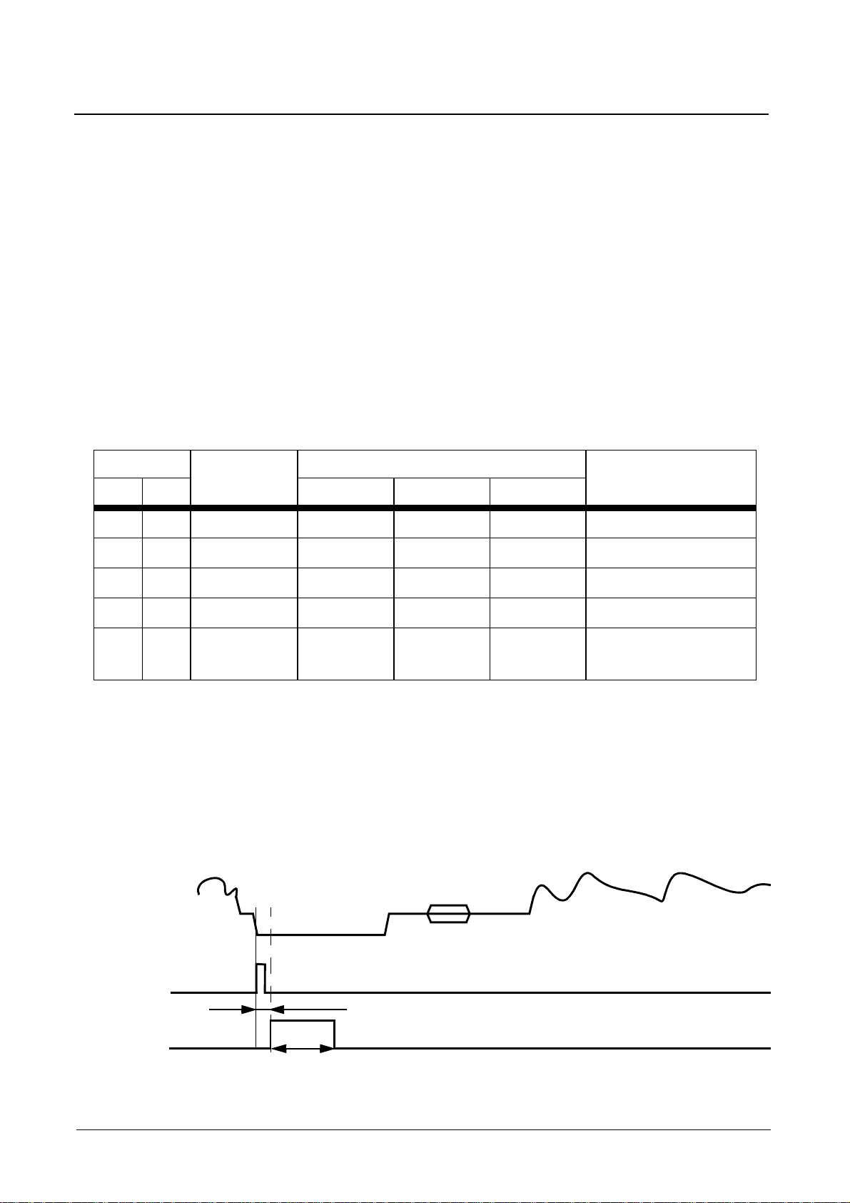
Figure 4-1 Clamping timing
Micronas 4-10
Page 11
SDA 9488X
SDA 9588X
Preliminary Data Sheet
System Description
The clamping pulse can be shifted in position (CLMPIST) and length (CLMPID) to adjust
to the specific application. The ADCs are driven by a 20.25 MHz free running crystal
clock which is not related to the incoming CVBS signal.
To avoid aliasing by subsampling the CVBS signal and the Y/C signals should be
bandlimited to 10MHz. In the same manner the U/V signal frequency spectrum (SDA
9588X) should not exceed 5 MHz. The digital filtering suppresses all frequencies above
the useable spectrum.
4.1.3 Automatic Gain Control
To accommodate to different CVBS input voltages an automatic gain control has been
implemented. The chip works correctly for input voltages in the range from 0.5 to 1.5V
pp
For best signal-to-noise ratio, the maximum CVBS amplitude is recommended if
available. The AGC behavior can be chosen out of four possibilities (AGCMDE):
The sync height serves as reference for the gain control in the typical application. When
using overflow detection only, the gain is set to maximum and is reduced whenever an
overflow occurs. This procedure will be executed again when a channel change is
detected or the gain control is manually reset by AGCRES.
.
2
1.5
1
Input Voltage [V]
0.5
0
0 2 4 6 8 10 12 14 16
Automatic Gain Control Characteristic
AGCVAL
Figure 4-2 AGC characteristic
4.1.4 Signal Magnitudes
The nominal CVBS signal with 75% color has a magnitude of 1 V
is left to permit signals with 100% color resulting in 1.23 V
pp
. The upper headroom
pp
. The Y signal must always
contain the sync part. Its levels correspond to the CVBS levels except for the missing
color and burst. After A/D conversion the video part is clamped to its black value and is
amplified to 224 digital steps. The nominal signal levels ensure correct brightness and
saturation. The YUV signal levels conform to the ITU 601 recommendation.
Micronas 4-11
Page 12
SDA 9488X
SDA 9588X
Preliminary Data Sheet
CRYC = 1.2 Vpp
255
224
128
32
burst
0
255
217
68
upper headroom
white
black
burst
4
0
lower headroom
SRY = 1 Vpp
Figure 4-3 CVBS/Y and chroma ADC input signal range
255
240
212
255
240
212
System Description
upper headroom
75% chroma
lower headroom
upper headroom upper headroom
100% chroma
SRC = 0.89 Vpp
CRYC = 1.2 Vpp
75% U
128
SRUV = 0.7 Vpp
44
16
0
lower headroom
Figure 4-4 UV input signal range
AGCVAL Conversion
D3 D2 D1 D0
Range
CRYC
0000 0.5Vpp0.42V
... ... ...
1000 1.2V
pp
... ... ...
CRUV = 0.8 Vpp
Signal
Range
SRY
1.0V
pp
128
44
16
pp
75% V
CRUV = 0.8 Vpp
SRUV = 0.7 Vpp
0
Signal
Range
SRC
0.89V
lower headroom
pp
Conversion
Range
CRUV
0.8V
pp
Signal
Range
SRUV
0.7V
pp
1111 1.5V
pp
1.25V
pp
Table 4-2 ADC conversion range and required input signal voltage
Micronas 4-12
Page 13
SDA 9488X
SDA 9588X
Preliminary Data Sheet
System Description
4.2 Inset Synchronization
Horizontal and vertical sync pulses are separated after elimination of the high frequency
components of the CVBS signal by a low pass filter. Horizontal sync pulses are
generated by a digital phase-locked-loop (DPLL). Its time constant is adjustable between
fast and slow behavior in four steps (PLLITC) to consider different input sources (e.g.
VCR). Noisy input signals become more stable when a noise-reduction is enabled
(NSRED). Additionally weak input signals from a satellite dish (’fishes’) become more
stable when SATNR is enabled. Both should be enabled to have best available
performance. When NOSIGB is enabled, a colored background is shown instead of the
picture when PIP is out of synchronization. The detected line standard is indicated by
SYNCSTAT.
4.3 Chroma Decoding And Standard Search
The system is able to decode NTSC and PAL signals with a subcarrier of 3.58MHz and
4.43MHz (PAL B/M/N/60, NTSC M/4.4) as well as SECAM signals with 4.05/4.2MHz
subcarrier. The system may be forced to a certain standard, or an automatic standard
detection can be used (CSTAND). For automatic standard detection, some standards
which are not likely to be received can be ignored to improve the detection process.
Depending on the detected line standard (525 or 625 lines) the color standard detection
circuit searches for 60 Hz signals (NTSC-M / PAL-M / PAL 60 / NTSC44) or 50 Hz signals
(PAL-B / SECAM / PAL-N) respectively. Within each line standard, the standard is
detected by consequently switching from one to another. This standard detection
process can be set to medium or fast behavior (LOCKSP). In medium behavior 30 fields
(in fast 20) are used to detect the standard. If not being successful within this time period
the system tries to detect another one. For SECAM detection, a choice between two
recognition levels is possible (SCMIDL) and the evaluated burstposition is selectable
(BGPOS).
.
CSTANDEX NTSC-
D1 D0
M
PAL60 PAL-N PAL-M PAL-B SECAM NTSC
44
00
0 .
1
10
11
Table 4-3 Considered color standards for automatic standard detection
For getting the chrominance information the digitized video signal is multiplied with the
regenerated color subcarrier once in-phase and once phase-shifted by 90°. After
lowpass filtering digital UV is available for PAL and NTSC. The subcarrier is regenerated
Micronas 4-13
Page 14
SDA 9488X
SDA 9588X
Preliminary Data Sheet
System Description
by a digital PLL. At SECAM operation the PLL runs free and generates the line-wise
alternating subcarriers. A CORDIC structure demodulates the frequency-modulated UV
signals. The following SECAM de-emphasis filter characteristic is adjustable (DEEMP).
The chroma signal can be filtered before demodulation by means of a selectable IFprefilter (IFCOMP).
0
5
10
gain [dB]
15
DEEMP = ’00’
DEEMP = ’01’
DEEMP = ’10’
DEEMP = ’11’
5
2.5
IFCOMP = ’00’
0
IFCOMP = ’01’
2.5
gain [dB]
IFCOMP = ’10’
5
7.5
3.58 4.4
20
0 0.5 1 1.5 2 2.5
frequency [MHz]
10
2 3 4 5 6
frequency [MHz]
Figure 4-5 SECAM de-emphasis filter characteristic and IF-compensation filter
characteristic
The Hue Control (HUE) influences the phase of the demodulation subcarrier between
-44.8° and 43.4° in steps of 1.4°. This is provided for NTSC only and adjustment is
ineffective for PAL and SECAM signals.
The reference for the subcarrier generation is a crystal stable clock of 20.25000 MHz. In
order to avoid color standard detection problems, the maximum deviation of this
frequency should not exceed 100ppm. For a good PLL locking behavior a maximum
deviation of 40ppm is recommended. A small frequency adjustment (-150 ... +310 ppm)
is possible for using a crystal with small frequency deviations (SCADJ). For test
purposes, CPLL allows to open the loop of the chroma PLL.
For deviations in the chroma signal up to 30dB, a stable output amplitude after chroma
decoding is achieved due to the ACC (Automatic Chroma Control). If the chroma signal
(color burst) is below a selectable threshold (CKILL), the color will be switched off.
Alternatively the color-killer can be bypassed and the color can be switched on or off
under all conditions (COLON). By setting ACCFIX, the automatic chroma control is
disabled and set to a default value.
Micronas 4-14
Page 15
SDA 9488X
SDA 9588X
Preliminary Data Sheet
System Description
CKILL COLON color killed at damping of
D1 D0
0 0 0 30 dB
0 1 0 18 dB
1 1 0 24 dB
1 1 0 color always off
X X 1 color always on
Table 4-4 Color-killer adjustment
The bandwidth of the chroma filter is adjustable via CHRBW. The bandwidth depends
on whether the decoder is in SECAM operation or not. A change in CHRBW does not
result in a chrominance position shift on the screen.
CKSTAT can be read out and gives information whether the color is switched on or off.
STDET indicates the detected color standard. Additionally PALID signals whether a PAL
signal or a NTSC signal is applied.
4.4 Comb Filtering
Depending on the selected picture size and color standard, a comb filtering is performed
for luminance and chrominance. A comb filter uses the spectral interleaving of the
encoded luminance and chrominance to separate both without cross artifacts. Thus
cross-color and cross-luminance are suppressed effectively. For NTSC sources, a comb
filtering is performed for all picture sizes. Due to reduced bandwidth in horizontal and
vertical direction a strong reduction of cross artifacts can be achieved for PAL signals.
The same applies for the luminance signal of SECAM signals.
4.5 Luminance Processing
The A/D-converted CVBS (or Y) signal is digitally clamped to back porch. Depending on
the transmitted standard and operational area, an offset between black- and blanking
level can be found in the incoming signal (’7.5 IRE’). As for some applications a black
offset is not desired, controlling may be done using LMOFST. The positive or negative
offset is added to the Y signal before scaling.
Micronas 4-15
Page 16
SDA 9488X
SDA 9588X
Preliminary Data Sheet
Received signal Processed signal
BLANK value
LMOFST
BLANK value
LMOFST
BLACK value
='00' (no additional offset)
BLACK value
='00' (no additional offset)
BLANK value
LMOFST
BLANK value
LMOFST
BLACK value
='10' (reduction of 16 LSB)
BLACK value
='01' (addition of 16 LSB)
Figure 4-6 Black level correction of luminance signal
System Description
M standard signals
B/G/H/I/N standard signals
The color carrier is removed out of a CVBS signal by means of a notch filter. It is set to
the corresponding color carrier (3.58 or 4.4 MHz) only if the standard is detected
permanently. This prevents the luminance sharpness of being changed within the
standard search process. For Y signals the notch is disabled.
For a fine adjustment of delaycompensation between luminance and chrominance,
YCDEL allows a luminance shifting in 16 steps of 50ns.
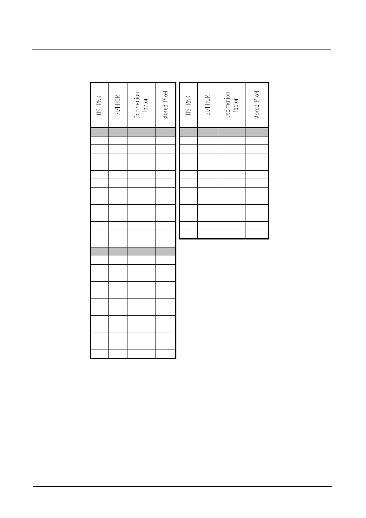
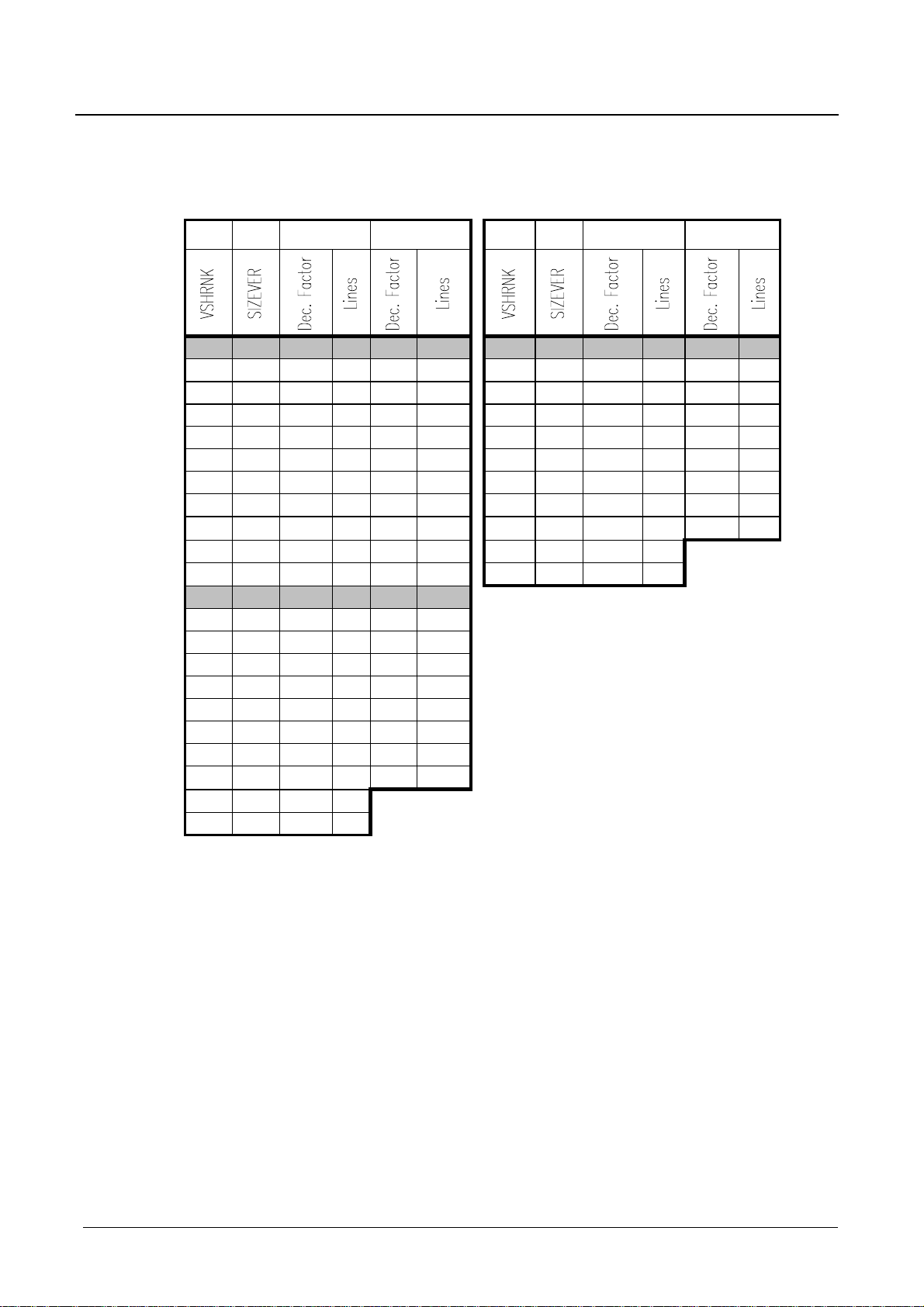
4.6 Decimation
4.6.1 Single PIP Mode
Luminance and chrominance signals are filtered in horizontal and vertical direction. The
coarse horizontal and vertical picture size (1/3, 1/4, 1/6) is independently programmable
with SIZEHOR and SIZEVER. A fine adjustment in steps of 4 pixel and 2 lines is possible
by HSHRINK and VSHRINK, which allows correct aspect ratio for multistandard
applications (50/60 Hz mixed mode, (S)VGA).
For main decimation factors, the stored number of pixel and lines are listed in the
following tables.
Micronas 4-16
Page 17
SDA 9488X
SDA 9588X
Preliminary Data Sheet
SIZEHOR horizontal
scaling
D1 D0
00 3:1
PIP Pixel per line
Y (B-Y) (R-Y)
1)
216 54 54
System Description
0 1 3:1 216 54 54
1 0 4:1 160 40 40
1 1 6:1 108 27 27
1)
only used for compatiblity with other SDA 948xX/958xX types
Table 4-5 Number of stored pixel per line dependent on SIZEHOR
SIZEVER vertical scaling PIP lines
D1 D0
00
1)
3:1 88 72
625 lines source 525 lines source
01 3:1 88 72
10 4:1 66 54
11 6:1 44 36
1)
only used for compatibility with other SDA 948xX/958xX types
Table 4-6 Number of stored lines per field
Micronas 4-17
Page 18
SDA 9488X
SDA 9588X
Preliminary Data Sheet
0 1 3,00 216 0 3 6,00 108
1 1 3,04 212 1 3 6,23 104
2 1 3,11 208 2 3 6,48 100
3 1 3,17 204 3 3 6,75 96
4 1 3,23 200 4 3 7,04 92
5 1 3,29 196 5 3 7,35 88
6 1 3,37 192 6 3 7,70 84
7 1 3,44 188 7 3 8,10 80
8 1 3,51 184 8 3 8,52 76
9 1 3,60 180 9 3 8,99 72
10 1 3,67 176 10 3 9,51 68
11 1 3,76 172 11 3 10,12 64
12 1 3,84 168 12 3 10,64 60
13 1 3,94 164
0 2 4,05 160
1 2 4,16 156
2 2 4,27 152
3 2 4,38 148
4 2 4,50 144
5 2 4,63 140
6 2 4,77 136
7 2 4,91 132
8 2 5,06 128
9 2 5,22 124
10 2 5,41 120
11 2 5,59 116
12 2 5,78 112
System Description
Table 4-7 Number of stored pixel per line dependent on HSHRNK
Micronas 4-18
Page 19
SDA 9488X
SDA 9588X
Preliminary Data Sheet
625 lines 525 lines 625 lines 525 lines
0 1 3,00 88 3 72 0 3 6,00 44 6,00 36
1 1 3,07 86 3,09 70 1 3 6,28 42 6,38 34
2 1 3,14 84 3,19 68 2 3 6,61 40 6,75 32
3 1 3,21 82 3,28 66 3 3 6,94 38 7,22 30
4 1 3,30 80 3,38 64 4 3 7,31 36 7,73 28
5 1 3,38 78 3,49 62 5 3 7,78 34 8,30 26
6 1 3,47 76 3,61 60 6 3 8,25 32 9,00 24
7 1 3,56 74 3,73 58 7 3 8,81 30 9,80 22
8 1 3,66 72 3,87 56 8 3 9,42 28 10,78 20
9 1 3,77 70 9 3 10,17 26
10 1 3,89 68 10 3 11,02 24
0 2 4,00 66 4,01 54
1 2 4,13 64 4,15 52
2 2 4,25 62 4,31 50
3 2 4,41 60 4,5 48
4 2 4,56 58 4,69 46
5 2 4,72 56 4,9 44
6 2 4,88 54 5,13 42
7 2 5,06 52 5,39 40
8 2 5,28 50 5,7 38
9 2 5,50 48
10 2 5,75 46
System Description
Table 4-8 Number of stored lines per field dependent on VSHRNK
4.6.2 Horizontal And Vertical Fine Positioning
All picture sizes are pre-centered inside the frame. In addition, if necessary the vertical
and horizontal acquisition area can be shifted by VFP for vertical and HFP for horizontal
direction.
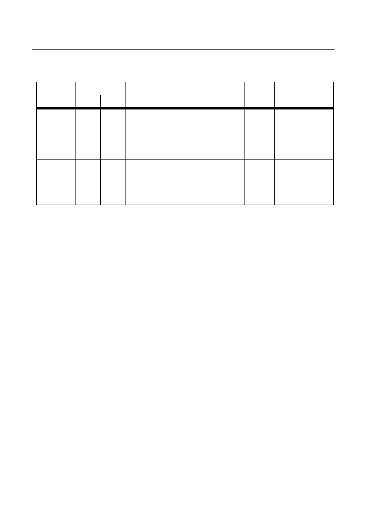
4.6.3 Multi Display Mode
SDA 9488X and SDA 9588X offer the feature to display a sub-picture more than once.
The picture size and arrangement depends on the display mode (DISPMOD) and not on
SIZEHOR or SIZEVER. Hence variable scaling is not possible in these modes.
Micronas 4-19
Page 20
SDA 9488X
SDA 9588X
Preliminary Data Sheet
Display
Mode
DISPMOD Size Picture
D1 D0 625 525
100SIZEHOR/
configuration
single PIP mode, 216
SIZEVER
HSRHNK/
System Description
Pixel Lines
88
-
60
-
24
72
-
20
VSHRNK
2 0 1 3 X1/9 one upon another
216 264 216
(same content)
3 1 0 4 X 1/16 one upon another
156 264 216
(same content)
Table 4-9 Multi-display modes
The display modes are shown in the appendix. The sizes of the partial pictures are listed
in table 4-9.
4.7 Display Control
The on-chip memory capacity is 512 kbits. Provided that the same standard (50 or 60
video sources are applied to inset and parent channel, jointline-free frame mode
Hz)
display is possible. This means that every incoming field is processed and displayed by
the SDA 9488X/SDA 9588X processor. The result is a high vertical and time resolution.
For this purpose the standard is analyzed internally and frame mode display is blocked
automatically, if the described restrictions are not fulfilled. Then only every second
incoming field is shown (field mode). Field mode normally shows jointlines. This is
caused by an update of the memory during read out. The result is that one part of the
picture contains new picture information and the other part contains one earlier written
field. The switching from or to frame mode is free of artifacts.
Activation of frame-mode display is blocked automatically if at least one of the following
conditions is not fulfilled:
• Inset and parent channel have the same field repetition frequency. This means that
frame mode is possible only for 50Hz inset and parent sources or 60Hz inset and
parent sources.
• Interlace signal is detected for inset and parent channel. For progressive scan or
(S)VGA display therefore only field mode is possible. For some VCRs in trick mode,
often no interlace is detected also.
• The number of lines is within a predefined range for inset (FMACTI) or parent
(FMACTP) channel (assuming standard signals according to ITU)
Micronas 4-20
Page 21
SDA 9488X
SDA 9588X
Preliminary Data Sheet
FMACTP parent
standard
number of
lines per field
FMACTI inset
standard
System Description
number of
lines per field
0 50 Hz 310...315 0 50 Hz 310...315
1 50 Hz 290...325 1 50 Hz 290...325
0 60 Hz 260...265 0 60 Hz 260...265
1 60 Hz 250...275 1 60 Hz 250...275
Table 4-10 Required number of lines for frame mode display
The system may be forced to field mode by means of FIESEL. Either first or second field
is selectable. ’One of both’ takes every second field independent of the field number.
This is meant for sources generating only one field (e.g. video-games).
For progressive scan conversion systems and HDTV / (S)VGA displays a line doubling
mode is available (PROGEN). Every line of the inset picture is read twice.
Memory writing is stopped by FREEZE bit. The field stored in the memory is then
continuously read. As the picture decimation is done before storing, the picture size of a
frozen picture can not be changed.
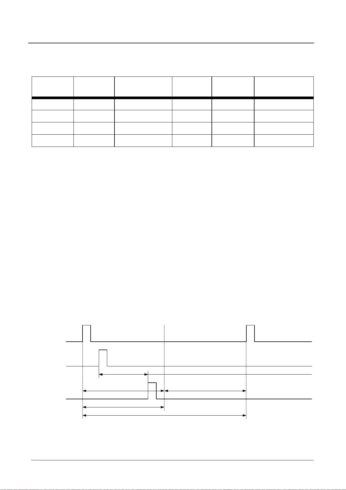
Depending on the phase between inset and parent signals a correction of the display
raster for the read out data is performed. Synchronization of memory reading with the
parent channel is achieved by processing the parent horizontal and vertical
synchronization signals. Horizontal and vertical pulses may be provided. The signals are
fed to the IC at pin HSP for horizontal synchronization and pin VSP for vertical
synchronization. HSPINV or VSPINV respectively allow an inversion of the expected
signal polarity.
HSP
VSP
VSPD
(internal)
VSPDEL VSPDEL
field 0 window field 1 window
←
tH/2 = 32 (16)
s
tH = 64 (32) ←s
=151 (75) ←s
max
values in brackets () apply for 100Hz systems
Figure 4-7 Field detection and phase adjustment of vertical pulse (VSP)
Micronas 4-21
Page 22
SDA 9488X
SDA 9588X
Preliminary Data Sheet
System Description
As the external VSP and HSP signals may come from different devices with different
delay paths, the phase between V-sync and H-sync is adjustable (VSPDEL). An
incorrect setting of VSPDEL may result in wrong or unreliable field detection of parent
channel.
Normally a noise reduction of the incoming parent vertical pulse is performed. With this
function missing vertical pulses are compensated. The circuit works for 50/60 Hz
applications as well as progressive and 100/120Hz application. (S)VGA signals are
supposed to be very stable and therefore not supported by the noise suppression. By
means of VSPNSRQ, vertical noise suppression is switched off.
A great variety of combinations of inset and parent frequencies are possible. The
following table shows some constellations:
Inset
Frequency
Parent
1)
Frequency
(HSP/VSP)
1)
frame
mode
correct aspect
ratio
(single pip)
correct aspect
ratio
(multi display)
vertical
noise
suppression
selectable
50 50i
50 60i
60 50i
60 60i
50 50p
50 60p
60 50p
60 60p
50 100i
50 120i
60 100i
60 120i
50 (S)VGA
60 (S)VGA
1)
standard signals supposed
2)
valid for some parent frequencies. Please refer to Chapter 4.7.1
2)
2)
Table 4-11 Available Features with varying inset and parent standards
Micronas 4-22
Page 23
SDA 9488X
SDA 9588X
Preliminary Data Sheet
4.7.1 Mixed Standard Applications And (S)VGA Support
remark
(N
apel
X N
aline
@ fV)
720X576@50Hz
(TV)
702X488@60Hz
(TV)
720X576@100Hz
(TV 100 Hz)
702X488@120Hz
(TV 120 Hz)
720X576@50Hz
(TV progressive)
fH
(kHz)
TH
←s)
(
T
Hact
←s)
15.6 64.0 52.0 625/
15.7 63.6 52.7 525/
31.2 32.0 26.0 625/
31.2 31.8 26.4 525/
31.2 32.0 26.0 625/
(
lines/
active
576
488
576
488
576
f
dot
(MHz)
13.5 interlace
13.5 interlace
27 interlace
27 interlace
27 prog-
System Description
scan correct
aspect
ratio
ressive
702X488@60Hz
(TV progressive)
640X480@60Hz
(VGA)
640X480@72Hz
(VGA)
640X480@75Hz
(VGA)
800X600@56Hz
(SVGA)
800X600@60Hz
(SVGA)
800X600@72Hz
(SVGA)
800X600@75Hz
(SVGA)
31.2 31.8 26.4 525/
488
31.5 31.8 25.4 525/
480
37.9 26.4 20.3 520/
480
37.5 26.7 20.3 500/
480
35.2 28.4 22.2 625/
600
37.9 26.4 20.0 625/
600
48.1 20.8 16.0 666/
600
46.9 21.3 16.2 625/
600
27 prog-
ressive
25.2 progressive
31.5 progressive
31.5 progressive
36.0 progressive
40.0 progressive
50.0 progressive
49.5 progressive
800X600@85Hz
(SVGA)
1024X768@43Hz
(SVGA)
53.7 18.6 14.2 631/
600
35.5 28.2 22.8 817/
768
Table 4-12 Examples of supported parent signals
Micronas 4-23
56.3 progressive
44.9 interlace
Page 24
SDA 9488X
SDA 9588X
Preliminary Data Sheet
System Description
The SDA 9488X resp. SDA 9588X allow multiple scan rates for the use in desktop video
applications, VGA compatible or 100Hz TV sets. All features are provided in ’normal’
operating modes at auto detected 50Hz and 60 Hz parent and inset standards. 2f
modes (100/120Hz and progressive) are supported by line frequency- and pixel clock
doubling and are not detected automatically. Even on a 16:9 picture tube correct aspect
ratio can be displayed by selecting the approbiate parent clock. The video synthesizer
generates also a special pixel clock for VGA display (see chapter 5.5.9 for details). As
(S)VGA consists of a variety of scan rates the correct aspect ratio is not adjustable for
all modes with the parent clock (HZOOM) because of the limited count of frequencies.
For single PIP only, correct aspect ratio is maintained by the vertical and horizontal
scaler (HSHRINK and VSHRINK).
It is possible to display (S)VGA sources for parent display, as long as the horizontal
frequency is lower than 40 kHz and the signal does not contain more than 1023 lines.
For progressive scan mode, PROGEN must be set. Additionally field-mode should be
forced to prevent unallowed frame-mode displaying (FIESEL). As the (S)VGA normally
does not fit to the display raster generated in the vertical noise suppression, VSPNSRQ
should be disabled. (S)VGA signals for inset channel are not supported.
H
PROGEN READD Expected input signal
0 0 50 or 60 Hz signal interlace
0 1 100 or 120 Hz signals interlace
1 0 (reserved)
1 1 50 or 60 Hz or (S)VGA signal progressive
Table 4-13 Selection of display field repetition
4.7.2 Display standard
For a single-PiP, the number of displayed lines depends on the selected picture size and
on the signal standard. For multi picture display, the number of displayed lines depends
on the selected picture size and on the signal standard of the parent signal. Additionally,
a standard can be forced by DISPSTD.
Micronas 4-24
Page 25
SDA 9488X
SDA 9588X
Preliminary Data Sheet
System Description
DISPSTD DISPMOD Display Standard
D1 D0
0 0 0 PIP depends on detected inset standard (single pip)
0 0 >0 PIP depends on detected parent standard (multi display)
0 1 x PIP display is always in 625 lines mode
1 0 x PIP display is always in 525 lines mode
1 1 x freeze last detected display standard and size
Table 4-14 Display standard selection
If a 625 lines picture is shown with a 525 lines parent signal, some lines are missing on
top and bottom of picture. If a 525 lines picture is shown with a 625 lines display
standard, missing lines at top and bottom are filled with background color.
4.7.3 Picture Positioning
The display position of the inset picture is programmable to the 4 corners of the parent
picture (CPOS). From there PIP can be moved to the middle of the TV Picture with
POSHOR and POSVER. The corner positions can be centered coarsely on the screen
with POSOFH and POSOFV. Depending on coarse position, one PIP corner remains
stable when changing the picture size.
CPOS Coarse
D1 D0
Position
Reference
corner of PiP
increasing
POSVER
increasing
POSHOR
0 0 upper left upper left down right
0 1 upper right upper right down left
1 0 lower left lower left up right
1 1 lower right lower right up left
Table 4-15 Coarse Positioning
Starting at every coarse position, the picture is movable to 256 horizontal locations (4
pixel increments) and 256 vertical locations (2 line increments). The pixel width on the
screen depends on the selected HZOOM factor. Even POP-positions (Picture Outside
Picture) in 16:9 applications are possible.
Micronas 4-25
Page 26
SDA 9488X
y
SDA 9588X
Preliminary Data Sheet
POSHOR
System Description
CPOS='01'
CPOS='00'
POSVER
CPOS='10'
CPOS='11'
POSHOR
POSVER
Figure 4-8 Coarse Positioning
4.8 Output Signal Processing
4.8.1 Luminance Peaking
To improve picture sharpness, a peaking filter which amplifies higher frequencies of the
input signal is implemented. The amount of peaking can be varied in seven steps by
YPEAK. The setting ’000’ switches off the peaking. The value ’011’ is recommended.
This provides a good compromise between sharpness impression and annoying
aliasing. The characteristic for all possible settings is shown in fig. (4-9)
10
9
8
7
6
5
gain [dB]
4
3
2
1
0
0 0.1 0.2 0.3 0.4 0.5
normed frequenc
YPEAK = ’111’
YPEAK = ’110’
YPEAK = ’101’
YPEAK = ’100’
YPEAK = ’011’
YPEAK = ’010’
YPEAK = ’001’
YPEAK = ’000’
Figure 4-9 Characteristics of selectable peaking factors
Micronas 4-26
Page 27
SDA 9488X
SDA 9588X
Preliminary Data Sheet
System Description
Coring should be switched on by YCOR to reduce noise, which is also amplified when
peaking is enabled. As the coring stage is in front of the peaking filter, 1 LSB noise will
not be peaked.
4.8.2 RGB Matrix
The chip contains three different matrices, one suited for EBU standards, one suited for
NTSC-Japan and one suited for NTSC-USA, which are selected via MAT. The signal
OUTFOR switches between YUV output or RGB output. The signal UVPOLAR inverts
the U and V channels and results in Y-U-V output. The standard magnitudes and angles
of the color-difference signals in the UV-plane are defined as follows:
MAT Magnitudes Angles Standard
D1 D0
(B-Y) (R-Y) (G-Y) (B-Y) (R-Y) (G-Y)
0 0 2.028 1.14 0.7 0 90 236 EBU
0 1 2.028 1.582 0.608 0 95 240 NTSC (Japan)
1 0 2.028 2.028 0.608 0 105 250 NTSC (USA)
1 1 (reserved)
Table 4-16 RGB matrices characteristics
The color saturation can be adjusted with SATADJ register in 16 steps between 0 and
1.875. Values above 1.0 may clip the chrominance signals.
4.8.3 Framing And Colored Background
Figure 4-10 Normal frame and 3D frame
Micronas 4-27
Page 28

SDA 9488X
SDA 9588X
Preliminary Data Sheet
System Description
With FRSEL a colored frame is added to the inset picture. The chip can display two
different types of frames, one simple monochrome frame and a more sophisticated
frame giving a three dimensional impression.
The frame elements are always placed outside the inset picture, except for the inner
shade of three dimensional frame or inner frame in multipip-mode. There is no shift of
the inset picture position if the inset frame width is modified.
4096 frame colors are programmable by FRY, FRU, and FRV, 4 bits for each
component. Horizontal and vertical width of the frame are programmable independently
by FRWIDH and FRWIDHV. If desired, frame color is displayed over the whole PIP size
or whole picture size of the main channel when PIPBG is set accordingly.
PiP Picture
background
picture
frame
no
frame color
background
no
background color
frame color
shades
no
dark/light
Figure 4-11 Selectable picture configurations
64 background colors are programmable by BGY, BGU, BGV, 2 bits for each
component. Alternatively BGFRC sets the background to frame color.
4.8.4 16:9 Inset Picture Support
To remove dark stripes at 16:9 inset pictures the vertical display area is reducable with
VPSRED. The number of omitted lines depends on the vertical decimation factor.
Micronas 4-28
Page 29

SDA 9488X
SDA 9588X
Preliminary Data Sheet
vertical
decimation
factor
displayed
lines (50Hz)
displayed
lines (50Hz)
with reduction
displayed
lines (60Hz)
System Description
displayed
lines (60Hz)
with reduction
1 264 214 216 175
...
644 35 36 29
Figure 4-12 Number of lines without and with reduction of vertical picture size
.
Figure 4-13 16:9 inset picture without and with reduction of vertical picture size
4.8.5 Parent Clock Generation
The phase of the output signals is locked to the rising edge of the horizontal sync pulse.
The frequency varies in a certain range to ensure correct aspect ratio for 16:9
applications depending on HZOOM. The horizontal and vertical scaling can be used for
all display frequencies.
display
format
inset
picture
format
desired
PiP format
required
parent
frequency
value of HZOOM
D2 D1 D0
4:3 4:3 4:3 27 000
4:3 4:3 16:9 20.25 0 0 1
16:9 4:3 4:3 36 0 1 0
16:9 16:9 16:9 36 0 1 0
Table 4-17 Format conversion using HZOOM
Micronas 4-29
Page 30

SDA 9488X
SDA 9588X
Preliminary Data Sheet
System Description
For variations of parental horizontal frequency (e.g. VCR), a digital correction of the
position is useful to stabilize the picture (POSCOR). This circuit detects a varying
parental line frequency and moves the picture to the place, where it would have been
without this frequency deviation. The calculation is done once a field.
4.8.6 Select Signal
For controlling an external RGB or YUV switch a select signal is supplied. The delay of
this signal is programmable for adaptation to different external output signal processing
devices (SELDEL). SELDOWN sets this output to tristate (high-resistance).
frame
picture
PiP signal
OUTx
SEL
SELDEL
Figure 4-14 Select timing
4.9 DA-Conversion And RGB / YUV Switch
The SDA 9588X/SDA 9488X include three 7bit DA-converters. Brightness (BRTADJ),
Contrast (CON) and overall amplitude (PKLR, PKLG, PKLB) of the output signal are
adjustable. External RGB or YUV signals can be connected to the inputs IN1...3. By
forcing the FSW input to high-level these signals are switched to the outputs OUT1...3
while the internal signals are switched off. The FSW input signal is passed through to the
SEL output. The setting of RGBINS determines wether an RGB insertion is possible and
which source, the external picture or the PiP, gets priority.
Micronas 4-30
Page 31

SDA 9488X
SDA 9588X
Preliminary Data Sheet
RGBINS='00'
PIPON='1'
CVBS1
VREFM
XINXQHSP
RGBINS='10'
PIPON='1'
OSD
R/V
G/Y
B/U
SEL
OUT3
OUT2
OUT1
VSSA2
VSSA1
VREFL
CVBS3
CVBS2
VSP
SDA
VDDA1
PiP IV
SCL
VDD
RGB/VYU
VDDA2
VREFH
VSS
I2C
INT
IN1
IN2
IN3
FSW SEL
FSW
OSD
RGBINS='11'
PIPON='1'
OSD
OSD
System Description
RGBIN='1X'
PIPON='0'
OSD
OSD
OSD
OSD
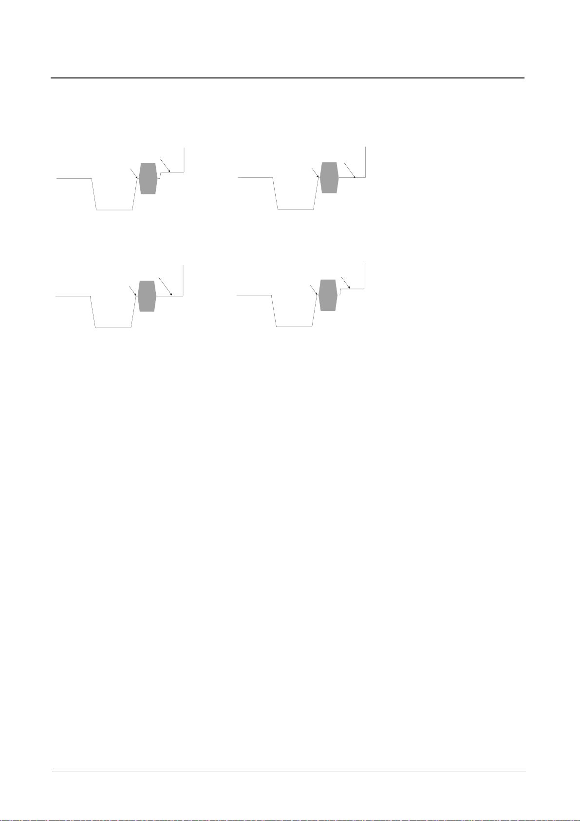
Figure 4-15 Visualization of RGB/YUV insertion
The external RGB or YUV signals are each clamped to the reference levels of the DACs
to force uniform black levels in each channel. The clamping needs careful adjustment
especially for VGA applications. The position and the length of the blanking pulse as well
as the clamping pulse are adjustable (CLPPOS, CLPLEN). If READD is set to ’1’ (100Hz
mode), all pulses are shortened by one half. HZOOM influences the adjustment range of
the clamping and blanking pulse because of the modified clock frequency, but the pulse
length is kept nearly constant.
Parent
Video
HSP
allowed
HSP range
BLANKP
a
256 T
b
CLAMPP
c
d
Figure 4-16 PIP horizontal blanking timing
Micronas 4-31
Page 32

SDA 9488X
SDA 9588X
Preliminary Data Sheet
READD CLPDEL CLPLEN a (←s)
D2 D1 D0 D1 D0
Blanking
Start
b (
←s)
Blanking
Duration
System Description
c (
←s)
Clamping
Start
Clamping
Duration
0 0 0 0 0 0 -1.5 10.5 3 5
011100 -11 10.5 -6.4 5
0 0 0 0 0 1 -1.5 7.9 2.2 3.8
0 1 1 1 0 1 -11.0 7.9 -7.3 3.8
1 0 0 0 0 0 -0.8 5.3 1.5 2.5
1 1 1 1 0 0 -5.5 5.3 -3.2 2.5
1 0 0 0 0 1 -0.8 4 1.1 1.9
1 1 1 1 0 1 -5.5 4 -3.6 1.9
Table 4-18 PIP horizontal blanking timing
d (
←s)
4.9.1 Contrast, Brightness and Peak Level Adjustment
The peak level adjustment modifies the magnitude of each channel separately. It should
be used to adapt once the signal levels to the following stage. The contrast adjustment
influences all three channels and allows a further increase of 30% of the peak level
magnitude. The effect of the brightness adjustment depends on the selected output
mode (RGB/YUV). In YUV mode it changes the offset of the OUT2 (Y) signal only while
in RGB mode it changes the offset of all three channels at the same time. The brightness
increase is up to 20%.
4.9.2 Pedestal Level Adjustment
The pedestal level adjustment controlled by I
2
C signals BLKLR, BLKLG, BLKLB
enables the correction of small offset errors, possibly appearing at the successive
blanking stage of RGB processor. This adjustment has an effect on the setup level
during the active line interval of each channel like the brightness adjustment but has an
enhanced resolution of 0.5 LSB. The maximum possible offset amounts to 7.5 LSBs. In
YUV mode (OUTFOR = ’1’) the action depends on the setting of BLKINVR and
BLKINVB. If BLKINVR (BLKINVB) is active the offset applies to the blank level of the
RV (BU) channel during the clamping interval for shifting the setup level to the negative
direction. In RGB mode (OUTFOR = ’0’) BLKINVR and BLKINVB have no effect.
Micronas 4-32
Page 33

SDA 9488X
SDA 9588X
Preliminary Data Sheet
YUV Mode
BLKINVR = BLKINVB = 0
BLKLR = 15
BLKLB = 15
32
BLKLR = 0
BLKLB = 0
RGB Mode
System Description
BLKINVR = BLKINVB = 1
BLKLR = 15
BLKLB = 15
32
BLKLR = 0
BLKLB = 0
BLKLR = 15
BLKLB = 15
BLKLG = 15
BLKLR = 0
BLKLB = 0
BLKLG = 0
0
Figure 4-17 Pedestal level adjustment
4.10 Data Slicer
Depending on SERVICE, Closed Caption data (’Line 21’) or WSS (Widescreen
2
signalling) is sliced by the digital data slicer and can be read out from I
C interface. The
line number of the sliced data is selectable with SELLNR. Therefore WSS and CC can
be processed in different regions (e.g. CC with PAL M). The Closed Caption data is
assumed to conform with the ITU standards EIA-608 and EIA-744-A. WSS data is
assumed to conform with ETS 300 294 (2nd edition, May 1996).
4.10.1 Closed Caption
The closed caption data stream contains different data services. In field 1 (line 21) the
captions CC1 and CC2 and the text pages T1 and T2 are transmitted whereas in field 2
(line 284) caption CC3, CC4, text T3, T4 and the XDS data are transmitted. For more
information please refer to the above mentioned standards.
Raw CC as well as prefiltered data is provided alternatively. With the built-in
programmable XDS-Filter (XDSCLS), the program-rating information (’V-chip’) as well
Micronas 4-33
Page 34

SDA 9488X
SDA 9588X
Preliminary Data Sheet
System Description
as others can be filtered out. The XDS filter reduce traffic on the I2C bus and save
calculation power of the main controller. If no class filter is selected, all incoming data
(both fields) is sliced and provided by the I
2
C interface. When one or more class filters
are chosen, only data in field 2 is sliced. Any combination of class filters is allowed. Each
’CLASS’ is divided into ’TYPES’ which can be sorted out by the XDS-secondary filter
(XDSTPE). Any combination of type filter is allowed. Some type filter require an
appropriate class filter.
4.10.2 Widescreen Signalling (WSS)
In WSS mode (SERVICE=’1’) no filtering is possible. All sliced data is passed to the
output registers. In this case XDSTPE selects the field number of the data to be sliced.
In Europe WSS carries for instance information about aspect ratio and movie mode.
4.10.3 Indication Of New Data
The sliced and possibly filtered data is available in DATAA and DATAB. The
corresponding status bits are DATAV and SLFIELD. When new data were received,
DATAV becomes ’1’ and the controller must read DATAA, DATAB and the status
information. After both data bytes were read DATAV becomes ’0’ until new data arrives.
It must be ensured that the data polling is activated once per field (16.7 or 20 ms) or
every second field (33.3 or 40 ms), depending on the slicer configuration and inset field
frequency. The field number of the data in DATAA and DATAB can be found in
SLFIELD. If one or more XDS-class filter are activated, SLFIELD contains always ’1’.
Additionally pin 10 (INT) may flag that new data is received. Default this pin is in tri-state
mode to be compatible with Micronas' SDA9388X/9389X PIP devices. It can also be
configured by IRQCON to output a single short pulse when new data is available or
behave equal to DATAV. In the last case the output remains active until the two data
registers DATAA/DATAB are read. Both modes are useful to avoid continuos polling of
the I2C bus. The micro-controller initiates I2C transfers only when required.
while (1){
i2c_read pip4_adr, status_reg_adr, status
if (status & data_valid_mask) {
i2c_read_inc pip4_adr, dataa_reg_adr, dataa, datab, status
process_data dataa, datab, status
}
}
Figure 4-18 Example in pseudo-code for reading the data
Micronas 4-34
Page 35

SDA 9488X
SDA 9588X
Preliminary Data Sheet
System Description
4.10.4 Violence Protection
The rating information is sent in the program rating packet of the current (sometimes
future) class in the XDS data stream. If only this information is desired the corresponding
XDS filter (class 01h, type 05h) should be used to suppress other data. The class/packet
bytes (0105h) precede the 2 bytes rating information. Each sequence is closed by the
end-of-packet byte (0fh) and a checksum. This checksum complements the byte
truncated sum of all bytes to 00h. Except comparison of the received rating with the
adjusted user rating threshold the micro-controller should check the parity of each byte
and validate the checksum to avoid miss-interpretation of wrong received data.
The SDA 9488X/SDA 9588X offer some alternatives to blocking the PIP channel
completely by switching it off (fig. (4-19)).
“Blue Screen” “Mosaic”“Warning Message”
THIS PROGRAM
CONTAINS VIOLENT
SCENES
Figure 4-19 Possibilities of PiP blocking
The Mosaic mode (MOSAIC) hides details of the picture by reduced sharpness and
increased aliasing. The picture looks scrambled and is less perceptible.
Micronas 4-35
Page 36

SDA 9488X
SDA 9588X
Preliminary Data Sheet
Application Examples
5 Application Examples
The following two figures show 100/120Hz applications with the Micronas Featurebox
SDA 9400/01. As the chip supports two I2C addresses and owns a RGB switch dual-PiP
applications are easy to implement. The arrangement for best possible performance is
shown in the fig. (5-1).
additional 1fH source
CVBS
(Y/C, YUV)
CVBS
(Y/C, YUV)
CVBS
(Y/C)
IN1-3
SDA9588X
HSP/VSP
OUT1-3
IN1-3
SDA9588X
HSP/VSP
OUT1-3
analog / digital
Frontend
I2C
I2C
+3.3V
H/V
YUV
1H
Featurebox
1H
i.e.SDA 9400
H/V
YUV
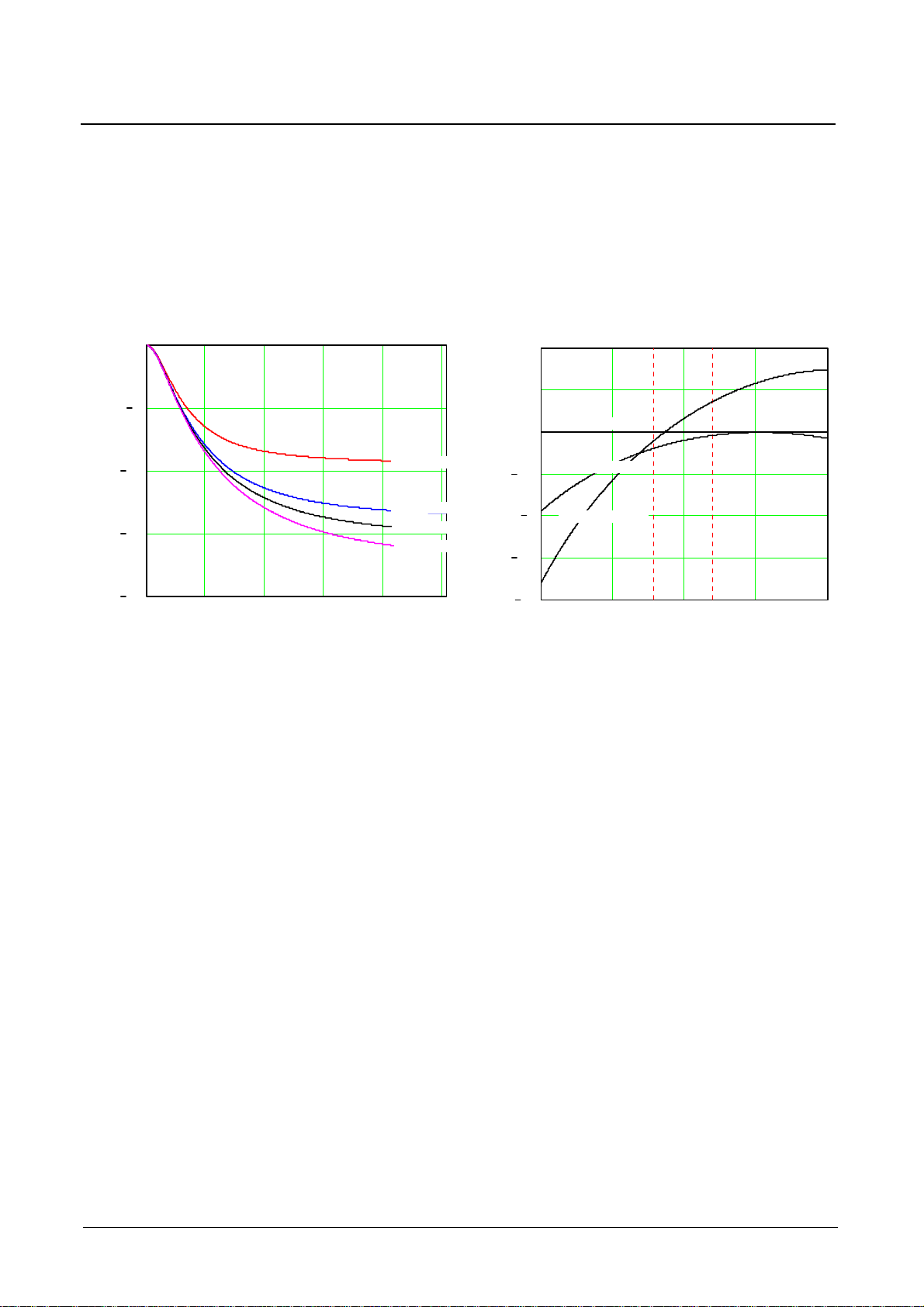
2H
2H
SDA9588X
SDA 9400
additional 2f
Backend
i.e. SDA9380
SDA9588X
sources
H
Figure 5-1 SDA 9588X application with insertion in front of the Featurebox
The output of two ’OCTOPUS’ are connected to the YUV (or RGB) input of the video
processor of the main channel. Due to the 4:2:2 processing within the SDA 9400 the
inset picture remains brilliant.
CVBS (Y/C)
SDA9588X
SDA 9400
analog / digital
Frontend
H/V
YUV
1H
Featurebox
1H
i.e. SDA 9400
CVBS
(Y/C, YUV)
H/V
YUV
SDA9588X
HSP/VSP
OUT1-3
I2C
additional 2fH sources
2H
Backend
2H
i.e. SDA9380
Figure 5-2 SDA 9588X application with insertion behind the featurebox
Connecting of a SDA 9588X directly to the RGB input of the RGB processor is possible
as well. One picture is generated from SDA 9588X device, the other one from the
featurebox. This cheap implementation preserves the chroma of inset channel at its full
bandwidth, although only field mode is possible for PiP picture. The output of an OSD/
Text processor may be fed to the RGB switch of the SDA 9588X.
Micronas 5-36
Page 37

SDA 9488X
SDA 9588X
Preliminary Data Sheet
6I
6.1 I
2
C Bus
2
C Bus Address
Write Address1 11010110 (D6h)
Read Address1 11010111 (D7h)
Table 6-1 Primary Address (pin 9=’low-level’)
Write Address2 11011110 (DEh)
Read Address2 11011111 (DFh)
Table 6-2 Secondary Address (pin 9 = ’high-level’)
I2C Bus
2
6.2 I
C-Bus Format
WRITE S 1101x110 A Subaddress A Data Byte A **** A P
READ S 1101x110 A Subaddress A Sr 1101x111 A Data Byte n NA P
S: Start condition / Sr Repeated start condition / A: Acknowledge / P: Stop condition /
NA: No Acknowledge
Write operation is possible at registers 00h-21h only, read operation is possible at
registers 28, 2Ah-2Ch only. An automatic address increment function is implemented.
Micronas 6-37
Page 38

SDA 9488X
SDA 9588X
Preliminary Data Sheet
I2C Bus
6.3 I2C bus Command Table
Subadd
(Hex)
D7 D6 D5 D4 D3 D2 D1 D0
00h PIPON CPOS1 CPOS0 YUVSEL READD PROGEN FIESEL1 FIESEL0
01h POSHOR7 POSHOR6 POSHOR5 POSHOR4 POSHOR3 POSHOR2 POSHOR1 POSHOR0
02h POSVER7 POSVER6 POSVER5 POSVER4 POSVER3 POSVER2 POSVER1 POSVER0
03h VFP3 VFP2 VFP1 VFP0 HFP3 HFP2 HFP1 HFP0
04h DISPSTD1 DISPSTD0 FREEZE MOSAIC SIZEHOR1
05h FPSTD1 FPSTD0 PIPBG1 PIPBG0 FMACTP HZOOM2 HZOOM1 HZOOM0
06h HSPINV VSPINV VSPNSRQ VSPDEL4 VSPDEL3 VSPDEL2 VSPDEL1 VSPDEL0
Data Byte
SIZEHOR0 SIZEVER1 SIZEVER0
07h FRSEL INFRM VPSRED FRWIDH2 FRWIDH1 FRWIDH0 FRWIDV1 FRWIDV0
08h RGBINS1 RGBINS0
09h POSCOR DISPMOD1 DISPMOD0 CLPDEL4 CLPDEL3 CLPDEL2 CLPDEL1 CLPDEL0
0Ah AGCRES AGCMD1 AGCMD0 AGCVAL3 AGCVAL2 AGCVAL1 AGCVAL0 NOSIGB
0Bh CVBSEL1 CVBSEL0 CLMPID1
0Ch PLLITC1
0Dh CSTAND2 CSTAND1 CSTAND0 CSTDEX1 CSTDEX0 LOCKSP CKILL1
0Eh BGPOS SCMIDL0 DEEMP1
0Fh IFCOMP1 IFCOMP0 HUE5 HUE4 HUE3 HUE2 HUE1 HUE0
10h SATNR FMACTI CPLLOF SCADJ4 SCADJ3
11h CONADJ3 CONADJ2 CONADJ1 CONADJ0 BLKLR3 BLKLR2 BLKLR1 BLKLR0
12h BRTADJ3 BRTADJ2 BRTADJ1 BRTADJ0 BLKLG3 BLKLG2 BLKLG1 BLKLG0
13h TRIOUT REFINT BLKINVR BLKINVB BLKLB3 BLKLB2 BLKLB1 BLKLB0
PLLITC0 NSRED1 NSRED0 YCDEL3 YCDEL2 YCDEL1 YCDEL0
VERBLK SELDOWN SELDEL3 SELDEL2 SELDEL1 SELDEL0
CLMPID0 CLMPIST1 CLMPIST0 LMOFST1 LMOFST0
CKILL0
DEEMP0 COLON ACCFIX CHRBW1 CHRBW0
SCADJ2 SCADJ1 SCADJ0
14h
15h
16h
PKLR7 PKLR6 PKLR5 PKLR4 PKLR3 PKLR2 PKLR1 PKLR0
PKLG7 PKLG6 PKLG5 PKLG4 PKLG3 PKLG2 PKLG1 PKLG0
PKLB7 PKLB6 PKLB5 PKLB4 PKLB3 PKLB2 PKLB1 PKLB0
Micronas 6-38
Page 39

SDA 9488X
SDA 9588X
Preliminary Data Sheet
Subadd
(Hex)
D7 D6 D5 D4 D3 D2 D1 D0
17h MAT1 MAT0 BGY1 BGY0 FRY3 FRY2 FRY1 FRY0
18h OUTFOR UVPOLAR BGU1 BGU0 FRU3 FRU2 FRU1 FRU0
19h (reserved) BGFRC BGV1 BGV0 FRV3 FRV2 FRV1 FRV0
1Ah
1Bh XDSCLS4 XDSCLS3 XDSCLS2 XDSCLS1 XDSCLS0 XDSTPE2 XDSTPE1 XDSTPE0
1Ch UVSEQ MPIPBG SERVICE SELLNR1
1Dh (reserved) (reserved) (reserved) (reserved) (reserved) PIPBLK PALIDL1 PALIDL0
1Eh POSOFV2 POSOFV1 POSOFV0 POSOFH4 POSOFH3 POSOFH2 POSOFH1 POSOFH0
1Fh (reserved) (reserved) (reserved) VSHRNK4 VSHRNK3 VSHRNK2 VSHRNK1 VSHRNK0
SATADJ3† SATADJ2 SATADJ1 SATADJ0† YPEAK2 YPEAK1 YPEAK0 YCOR
Data Byte
SELLNR0 IRQCON2 IRQCON1 IRQCON0
I2C Bus
20h (reserved) (reserved) (reserved) HSHRNK4 HSHRNK3 HSHRNK2 HSHRNK1 HSHRNK0
21h (reserved) (reserved) (reserved) (reserved) (reserved) (reserved) CLPLEN1 CLPLEN0
28h FRMMD PIPSTAT SYNCST1 SYNCST0 CKSTAT STDET2 STDET1 STDET0
2Ah DATAA7 DATAA6 DATAA5 DATAA4 DATAA3 DATAA2 DATAA1 DATAA0
2Bh DATAB7 DATAB6 DATAB5 DATAB4 DATAB3 DATAB2 DATAB1 DATAB0
2Ch DEVICE1 DEVICE0 PRNSTD PALID DATAV SLFIELD
After power on the grey marked data bits are set to '1', all other to ‘0‘.
Micronas 6-39
Page 40

SDA 9488X
SDA 9588X
Preliminary Data Sheet
6.4 I2C Bus Command Description
Subaddress 00h
PIPON PiP on
D7 switches the PIP insertion on
0 PIP insertion off
1 PIP insertion on
CPOS Coarse position
D6 D5 coarse positioning of the picture
0 0 upper left position
0 1 upper right position
1 0 lower left position
I2C Bus
1 1 lower right position
YUVSEL YUV Select
D4 select YUV mode
0 CVBS or Y/C source
1 YUV source
READD Read Double Mode
D3 double read frequency for compatibility with systems that use 2fH
(e.g.100 Hz, progressive)
0 PIP display with single read frequency and 2x oversampling
1 PIP display with double read frequency
Micronas 6-40
Page 41

SDA 9488X
SDA 9588X
Preliminary Data Sheet
PROGEN Progressive Scan Enable
D2 for compatibility with progressive scan systems
0 each line of PIP is read once (normal operation)
1 each line of PIP is read twice (line doubling operation)
FIESEL Field Select
D1 D0 set field or frame display mode
0 0 frame mode (if possible)
0 1 field mode (first field only)
1 0 field mode (second field only)
1 1 field mode (one of both)
I2C Bus
Subaddress 01h
POSHOR Horizontal Picture Position
D7-D0 horizontal position adjustment of the PIP in steps of 4 pixel
shift direction depends on the coarse positioning of the picture
Subaddress 02h
POSVER Vertical Picture Position
D7-D0 vertical position adjustment of the PIP in steps of 1 lines
shift direction depends on the coarse positioning of the picture
Micronas 6-41
Page 42

SDA 9488X
SDA 9588X
Preliminary Data Sheet
Subaddress 03h
HFP Horizontal Fine Positioning
D7 D6 D5 D4 changes the position of the horizontal
acquisition window by steps of 2 pixel
1000-16 pixel (-0.8 ←s), most right position of
the image
..
00000 pixel, nominal center position
..
0111+14 pixel (0.7 ←s), most left position
VFP Vertical Fine Positioning
I2C Bus
Note
values refer to
the
undecimated
picture
D3 D2 D1 D0 changes the position of the vertical
Note
acquisition window by steps of 1 line
1000-8 lines, most upper position of the imagevalues refer to
..
the
undecimated
00000 lines, nominal center position
picture
..
0111+7 lines, most right position
Subaddress 04h
DISPSTD Display Standard
D7 D6 selects the line standard of PIP display
0 0 PIP depends on detected inset standard
0 1 PIP display is always in 625 line mode
1 0 PIP display is always in 525 line mode
1 1 freeze last detected display standard and size
Micronas 6-42
Page 43

SDA 9488X
SDA 9588X
Preliminary Data Sheet
FREEZE Freeze Picture
D5 interrupts the inset picture writing and displays still picture
0 live picture
1 still picture
MOSAIC Mosaic Mode
D4 hides picture details, intended for use with parental control
0 mosaic mode off
1 mosaic mode on
SIZEHOR Horizontal Size
I2C Bus
D3 D2 horizontal decimation
0 0 reduction = 2
0 1 reduction = 3
1 0 reduction = 4
1 1 reduction = 6
SIZEVER Vertical Size
D1 D0 vertical decimation
0 0 reduction = 2
0 1 reduction = 3
1 0 reduction = 4
1 1 reduction = 6
Micronas 6-43
Page 44

SDA 9488X
SDA 9588X
Preliminary Data Sheet
Subaddress 05h
FPSTD Force Parent Standard
D7 D6 forces the parent standard to one of the following modes
0 0 auto-detect parent standard
0 1 50Hz/625 lines parent standard forced
1 0 60Hz/525 lines parent standard forced
1 1 freeze last detected standard
PIPBG PIP Background Display
D5 D4 selects the background display
0 0 PIP visible, no background display
0 1 PIP invisible, background display in PIP
I2C Bus
1 0 PIP visible, full screen background display
1 1 PIP invisible, background display in PIP and full screen background
FMACTP Frame Mode Activation Parent
D3 selects the parent condition for the activation of the frame mode
0 Frame mode active for standard parent video sources only
1 Frame mode active for some nonstandard sources also
HZOOM Horizontal Zoom
D2 D1 D0 selects the parent (display) clock frequency
0 0 0 27.34 MHz
0 0 1 20.25 MHz
0 1 0 35.27 MHz
0 1 1 25.43 MHz
1 0 0 26.67 MHz
1 0 1 20.63 MHz
1 1 0 34.17MHz
1 1 1 28.04 MHz
Micronas 6-44
Page 45

SDA 9488X
SDA 9588X
Preliminary Data Sheet
Subaddress 06h
HSPINV Horizontal Sync Pulse Inversion
D7 inverts the polarity of HSP
0 no inversion, raising edge is sync reference
1 HSP inverted, falling edge is sync reference
VSPINV Vertical Sync Pulse Inversion
D6 inverts the polarity of VSP
0 no inversion, raising edge is sync reference
1 VSP inverted, falling edge is sync reference
I2C Bus
VSPNSRQ Vertical Sync Pulse Noise Reduction
D5 activates automatic V insertion that generates vertical sync pulses in
case of missing external VSP
0on
1off
VSPDEL Vertical Sync Pulse Delay
D4 D3 D2 D1 D0 delay of the vertical sync pulse
in steps of 128 parent clocks
00000no delay (0) delay
...
11111maximum delay, 4096 clocks of
parent frequency
Subaddress 07h
Note
depends on
HZOOM
FRSEL Frame Select
D7 selects between the normal frame and the shaded frame
0normal frame
1 shaded frame with 3D impression
Micronas 6-45
Page 46

SDA 9488X
SDA 9588X
Preliminary Data Sheet
INFRM Inner Frame activation
D6 actives inner frame (4 pix. width, 2 lines height) for displ. mode 2 and 3
0 inner frame off
1 inner frame on
VPSRED Vertical Picture Size Reduction
D5 reduces vertical picture size to suppress black bars in 16:9 programs
0 no reduction
1 reduction on
FRWIDH Frame Width Horizontal
D4 D3 D2 adjusts the horizontal width of the PIP frame in steps of one
pixel
I2C Bus
0 0 0 no horizontal frame
...
1117 pixel
FRWIDV Frame Width Vertical
D1 D0 adjusts the vertical width of the PIP frame in steps of one line
0 0 no vertical frame
...
1 1 3 lines
Subaddress 08h
RGBINS RGB Insertion
D7 D6 controls the insertion of external RGB/YUV sources
0 0 no external insertion possible, FSW input inactive
0 1 external insertion forced (FSW = 1)
1 0 external insertion with FSW possible (priority of FSW input)
1 1 external insertion with FSW possible (priority of PIP)
Micronas 6-46
Page 47

SDA 9488X
SDA 9588X
Preliminary Data Sheet
VERBLK Vertical Blanking
D5 switches the vertical blanking mode
0 blanking level at DAC outputs only during line-blanking intervals
1 blanking level at DAC outputs during line-blanking intervals and field-
blanking intervals, 16 lines following the parent vertical synchronization
pulse are blanked
SELDOWN Select Down
D4 switches the driver type at the output of the SEL pin
0 open source output
I2C Bus
1 TTL output
SELDEL Select Delay
D3 D2 D1 D0 adjusts the delay of select signal
1 0 0 0 -8 clock periods of display clock
..
0 0 0 0 0 clock periods of display clock
..
0 1 1 1 +7 clock cycles of display clock
Subaddress 09h
POSCOR Position Correction
D7 activates correction of display position
0 position correction disabled
1 position correction enabled
Micronas 6-47
Page 48

SDA 9488X
SDA 9588X
Preliminary Data Sheet
I2C Bus
DISPMOD Display Mode
D6 D5 selects display modes with equal pictures
0 0 single PiP mode
0 1 3 x1/9 PiP (same content)
1 0 4 x1/16 PiP (same content)
1 1 (reserved)
CLPDEL Clamping Delay
D4 D3 D2 D1 D0 delay of the clamping pulse for the external RGB/YUV
inputs in steps of 8 parent clock periods
0 0 0 0 0 no delay (0)
...
1 1 1 1 1 maximum delay, 256 clock periods of parent
frequency
Subaddress 0Ah
AGCRES Automatic Gain Control Reset
D7 resets AGC
0 normal operation
1 reset of AGC
AGCMD AGC Mode
D6 D5 controls the AGC operation
0 0 evaluation of sync height and ADC overflow
0 1 evaluation of sync height only
1 0 evaluation of ADC overflow only
1 1 AGC fixed (gain depends on AGCVAL)
Micronas 6-48
Page 49

SDA 9488X
SDA 9588X
Preliminary Data Sheet
AGCVAL Automatic Gain Control Value
D4 D3 D2 D1 AGC value for fixed mode (AGCMD=’11’)
0 0 0 0 input voltage 0.5 Vpp
..
1 0 0 0 input voltage 1 Vpp
..
1 1 1 1 input voltage 1.5 Vpp
NOSIGB No Signal Behavior
D0 controls behavior if synchronization is not possible (no source applied)
0 noisy picture
1 colored background
I2C Bus
Subaddress 0Bh
CVBSEL CVBS Select
D7 D6 select CVBS source
0 0 CVBS1
0 1 CVBS2
1 0 Y/C (Y@CVBS2 / C@CVBS3)
1 1 CVBS3
CLMPID Clamping Duration
D5 D4 adjusts duration of clamping pulse for ADC (inset channel)
000.5←s
010.9←s
101.2←s
111.5←s
Micronas 6-49
Page 50

SDA 9488X
SDA 9588X
Preliminary Data Sheet
I2C Bus
CLMPIST Clamping Pulse Start
D3 D2 adjusts delay of clamping pulse for ADC refered to the horizontal sync
001.0←s
011.5←s
102.0←s
112.5←s
LMOFST Luminance Offset
D1 D0 modifies black to blank level offset
0 0 no offset
0 1 offset of 16 LSB
1 0 offset of -8 LSB
1 1 offset of -16 LSB
Subaddress 0Ch
PLLITC Inset PLL Time Constant
D7 D6 switches the time constant of the inset PLL
0 0 VCR1 (very fast)
01VCR2
10TV1
1 1 TV2 (very slow)
NSRED Noise Reduction Inset PLL
D5 D4 selects the level of noise reduction Note
0 0 noise reduction disabled
0 1 weak noise reduction may cause trouble for VCR
1 0 heavy noise reduction
signals
1 1 medium noise reduction
Micronas 6-50
Page 51

SDA 9488X
SDA 9588X
Preliminary Data Sheet
YCDEL Y/C Delay
D3 D2 D1 D0 adjusts the delay between luminance and chrominance
1 0 0 0 -8 pixel (-0.4 ←s with respect to undecimated picture)
..
0000 0 pixel
..
0 1 1 1 +7 pixel (0.35 ←s)
Subaddress 0Dh
CSTAND Color Standard
D7 D6 D5 forces the desired color standard
0 0 0 automatic standard identification
I2C Bus
001NTSC-M
0 1 0 PAL-N (Argentina)
011PAL-M
100 NTSC44
101PAL-B
1 1 0 SECAM
111PAL60
CSTDEX Color Standard Exclusion
D4 D3 excludes standards from automatic standard identification
0 0 ignore PAL-M / PAL-N
0 1 ignore SECAM, PAL B/G, PAL60, NTSC4.4
1 0 ignore PAL-M /PAL-N / NTSC-M
1 1 ignore PAL-M / PAL-N / NTSC4.4 / PAL60
LOCKSP Standard Identification Speed
D2 sets the speed of the color standard recognition
0 medium
1fast
Micronas 6-51
Page 52

SDA 9488X
SDA 9588X
Preliminary Data Sheet
CKILL Color Killer Threshold
D1 D0 damping of color carrier to switch color off Note
0 0 -30 dB only valid if color killer
0 1 -18 dB
active (COLON=’0’),
values are
1 0 -24 dB
approximative
1 1 color always off
Subaddress 0Eh
BGPOS Burst Gate Position
D7 adjusts position of burst gate
0 normal position
I2C Bus
10.5 ←s delayed
SCMIDL SECAM Identification Level
D6 changes SECAM identification sensitivity
0 default
1 enhanced
DEEMP Deemphase Selection
D5 D4 adjusts SECAM deemphase filter
00Filter1
0 1 ITU recommendation
10Filter2
11Filter3
COLON Color On
D3 disable color killer
0 color killer active
1 color forced on
Micronas 6-52
Page 53

SDA 9488X
SDA 9588X
Preliminary Data Sheet
ACCFIX Disable Automatic Chroma Control
D2 disables the automatic chroma control (ACC)
0 ACC active
1 ACC fixed (ACC set to nominal value)
CHRBW Chroma Bandwidth
D1 D0 PAL SECAM remark
0 0 wide small adjusts chroma bandwidth
0 1 medium medium
1 0 reserved
11small wide
I2C Bus
Subaddress 0Fh
IFCOMP IF-Compensation Filter
D7 D6 equalizes the IF-stage characteristic
0 0 no filtering
0 1 chroma bandpass active
1 0 IF-compensation bandpass (6dB/octave)
1 1 reserved
HUE Hue Control
D5 D4 D3 D2 D1 D0 phase of color
remark
subcarrier for NTSC
1 0 0 0 0 0 -44.8° skin color becames
greenish
..
0000000°
..
0 1 1 1 1 1 43.4° skin color becomes
redish
Micronas 6-53
Page 54

SDA 9488X
SDA 9588X
Preliminary Data Sheet
Subaddress 10h
SATNR Satellite Noise Reduction
D7 stabilizes the horizontal PLL for bad satellite signals („fishes“)
0 disabled
1 enabled
FMACTI Frame Mode Activation Inset
D6 sets the inset condition for the activation of the frame mode
0 frame mode only active for standard inset video sources
1 enhanced frame mode activation range
CPLLOF Chroma PLL Off
D5 opens loop of chroma PLL (only for test and servicing)
I2C Bus
0 chroma PLL active
1 chroma PLL opened (free running oscillator)
SCADJ Color Subcarrier Adjustment
D4 D3 D2 D1 D0 color subcarrier frequency fine adjustment
0 0 0 0 0 max. negative deviation (-150 ppm)
...
0 0 1 1 1 default (for nominal crystal frequency
...
1 1 1 1 1 max. positive deviation (+310 ppm)
Subaddress 11h
CONADJ Contrast Adjustment
D7 D6 D5 D4 adjusts the contrast of the picture, acts on OUT1-OUT3
0000nominal contrast
..
1111+30% contrast increase
Micronas 6-54
Page 55

SDA 9488X
SDA 9588X
Preliminary Data Sheet
I2C Bus
BLKLR Blanking Level Red
D3 D2 D1 D0 adjusts the pedestal level of the OUT1 channel in steps of
0.5LSB
0 0 0 0 no pedestal
..
1 1 1 1 +7.5LSB offset
Subaddress 12h
BRTADJ Brightness Adjustment
D7 D6 D5 D4 adjusts the brightness of the picture, acts on OUT1-OUT3 in
RGB mode (YUVFOR = ’0’) and on OUT1 in YUV mode
(YUVFOR = ’1’)
0 0 0 0 nominal brightness
..
1 1 1 1 +20% brightness increase
BLKLG Blanking Level Green
D3 D2 D1 D0 adjusts the pedestal level of the OUT2 channel in steps of
0.5LSB
0 0 0 0 no pedestal
..
1 1 1 1 +7.5LSB offset
Subaddress 13h
TRIOUT Tristate Output
D7 sets OUT1-OUT3 to tristate mode (high resistance)
0 normal operation, outputs are active
1 pins OUT1-3 are in tri-state mode
Micronas 6-55
Page 56

SDA 9488X
SDA 9588X
Preliminary Data Sheet
REFINT Refresh Intervall
D6 changes the refresh rate of eDRAM Note
0 normal refresh let it to this default value
1 fast refresh
BLKINVR Blanking Inversion Red
D5 inverts the sign of the OUT1 channel offset (BLKLR)
0 offset added during the active picture
1 offset added during blanking
BLKINVB Blanking Inversion Blue
D4 inverts the sign of the OUT3 channel offset (BLKLB)
I2C Bus
0 offset added during the active picture
1 offset added during blanking
BLKLB Blanking Level Blue
D3 D2 D1 D0 adjusts the pedestal level of the OUT3 channel in steps of
0.5LSB
0000no pedestal
..
1111+7.5LSB offset
Micronas 6-56
Page 57

SDA 9488X
SDA 9588X
Preliminary Data Sheet
Subaddress 14h
PKLR Peak Level Red
D7 D6 D5 D4 D3 D2 D1 D0 peak to peak output
voltage of the
OUT1 channel
000000000.3 V
pp
...
110000001 V
pp
...
111111111.2 V
pp
Subaddress 15h
I2C Bus
Note
values refer to
contrast
(CONADJ)
and
brightness
(BRTADJ) at
minimum
PKLG Peak Level Green
D7 D6 D5 D4 D3 D2 D1 D0 peak to peak
output voltage of
the OUT2 channel
000000000.3 V
pp
...
110000001 V
pp
...
111111111.2 V
pp
Note
values refer to
contrast
(CONADJ)
and
brightness
(BRTADJ) at
minimum
Micronas 6-57
Page 58

SDA 9488X
SDA 9588X
Preliminary Data Sheet
Subaddress 16h
PKLB Peak Level Blue
D7 D6 D5 D4 D3 D2 D1 D0 peak to peak
output voltage of
the OUT2 channel
000000000.3 V
pp
...
110000001 V
pp
...
111111111.2 V
pp
Subaddress 17h
I2C Bus
Note
values refer
to contrast
(CONADJ)
and
brightness
(BRTADJ)
at minimum
MAT RGB Matrix Select
D7 D6 selects the RGB matrix coefficients for YUV to RGB conversion
0 0 EBU- Matrix
0 1 NTSC-Japan Matrix
1 0 NTSC-USA Matrix
1 1 (reserved)
BGY Background Color Y
D5-D4 adjusts the Y background color component
the values gives the two MSBs of the Y background signal
FRY Frame Color Y
D3-D0 adjusts the Y frame color component
the value gives the 4 MSBs of the Y frame signal
Micronas 6-58
Page 59

SDA 9488X
SDA 9588X
Preliminary Data Sheet
Subaddress 18h
OUTFOR Output Format
D7 switches between RGB output and YUV output
0 RGB output signals, matrix active
1 YUV output signals
UVPOLAR UV Polarity
D6 switches between UV or inverted UV output, has no influence in RGB
mode
0 +U / +V output
1 -U / -V output
BGU Background Color U
I2C Bus
D5-D4 adjusts the U background color component
the values gives the two MSBs of the U background signal
FRU Frame Color U
D3-D0 adjusts the U frame color component
the value gives the 4 MSBs of the U frame signal
Subaddress 19h
BGFRC Background Frame Color
D6 selects background color table or frame color table for background
color
0 background color according to BGY, BGU, BGV
1 background color according to FRY, FRU, FRV
BGV Background Color V
D5-D4 adjusts the V background color component
the values gives the two MSBs of the V background signal
Micronas 6-59
Page 60

SDA 9488X
SDA 9588X
Preliminary Data Sheet
FRV Frame Color V
D3-D0 adjusts the V frame color component
the value gives the 4 MSBs of the V frame signal
Subaddress 1Ah
SATADJ Color Saturation Adjustment
D7 D6 D5 D4 adjusts the color saturation in steps of x/8
0000no color
..
1000nominal saturation
..
11111.875 times saturation
I2C Bus
YPEAK Y Peaking Adjustment
D3 D2 D1 adjusts luminance peaking
0 0 0 no peaking
0 1 1 recommended value
1 1 1 strongest peaking
YCOR Y Coring Enable
D0 suppresses noise introduced by peaking
0 coring off
1 1LSB coring
Micronas 6-60
Page 61

SDA 9488X
SDA 9588X
Preliminary Data Sheet
Subaddress 1Bh
XDSCLS XDS Class Select
D7 D6 D5 D4 D3 Closed Caption XDS-Primary Filter (Class)
00000transparent, no filtering
1XXXX’Current’ class selected
X 1 X X X ’Future’ class selected
X X 1 X X ’Channel’ class selected
X X X 1 X ’Miscellaneous’ class selected
XXXX1’Public Services’ class selected
XDSTPE XDS Type Select
D2 D1 D0 XDS-Secondary
Filter Type
Meaning WSS
field
I2C Bus
Note
0 0 0 all no filtering 0 behavior of
0 0 1 05h program rating 1
these bits
depends
0 1 0 01h, 04h time information
only
0 1 1 40h out of band only 0/1
1 0 0 01h, 02h, 03h, 04h,
VCR information 0/1
0/1
on
selected
dataservice
0Dh, 40h
1 0 1 01h, 04h, 05h time information
0/1
and program rating
1 1 0 05h, 40h out of band and
0/1
program rating
1 1 1 01h, 02h, 03h, 04h,
05h, 0Dh, 40h
VCR information
and program rating
0/1
Subaddress 1Ch
UVSEQ UV Sequence
D7 changes the UV multiplex sequence (valid only if YUVSEL=’1’)
0 U and V are correct
1 U and V are exchanged
Micronas 6-61
Page 62

SDA 9488X
SDA 9588X
Preliminary Data Sheet
MPIPBG Multi-PIP Background
D6 selects the background color for multi-PIP mode
0 black (8 IRE)
1 same as background color
SERVICE Data Service Select
D5 selects data service for slicing
0Closed Caption
1 Widescreen Signalling (WSS)
SELLNR Select Line Number
D4 D3 line number of data service field 0 (field1) remark
I2C Bus
0 0 [NTSC] 20 (283), [PAL M] 17 (280) WSS
0 1 [NTSC] 21 (284), [PAL M] 18 (281) Closed Caption
1 0 [PAL B/G] 22 (329) Closed Caption
1 1 [PAL B/G] 23 (330) WSS
IRQCON Interrupt Request Pin Configuration
D2 D1 D0 output of INT pin is: remark
0 0 0 tri-state (high-Z)
0 0 1 interrupt, when new data received
(pos. polarity)
pulse length is
approximately 2←s
0 1 0 interrupt, when new data received
(neg. polarity)
0 1 1 equivalent to DATAV for both
registers (pos. polarity)
1 0 0 equivalent to DATAV for both
registers (neg. polarity)
1 0 1 inset V-pulse (50ns) pulse length is 50ns
1 1 0 inset field high=first field, low =
second field
1 1 1 inset clamping pulse only for test purpose
Micronas 6-62
Page 63

SDA 9488X
SDA 9588X
Preliminary Data Sheet
Subaddress 1Dh
PIPBLK PIP Blank
D3 blanks the picture by setting it to background color
0 no blank
1 blanks the PIP
PALIDL PAL ID Level
D1 D0 sensitivity of identification of PAL/NTSC signals
0 0 high recjection of PAL/NTSC
..
1 1 low rejection of PAL/NTSC
I2C Bus
Subaddress 1Eh
POSOFV Position Offset Vertical
D7 D6 D5 vertical position offset in steps of 4 lines
100-16 lines
...
0000 lines
...
0 1 1 +12 lines
POSOFH Position Offset Horizontal
D4 D3 D2 D1 D0 horizontal position offset in steps of 16 pixel
10000-256 pixel
...
000000 pixel
...
01111+240 pixel
Micronas 6-63
Page 64

SDA 9488X
SDA 9588X
Preliminary Data Sheet
Subaddress 1Fh
VSHRNK Vertical Shrink
D4 D3 D2 D1 D0 changes the vertical size in steps of 2
lines
0 0 0 0 0 no shrink, picture size according to
SIZEVER
...
11111max. possible shrink
Subaddress 20h
HSHRNK Horizontal Shrink
D4 D3 D2 D1 D0 changes the horzontal size in steps of
4 pixel
I2C Bus
Note
max. usable
value
depends on
SIZEVER
Note
00000no shrink, picture size according to
SIZEHOR
...
max. usable
value
depends on
SIZEVER
11111max. possible shrink
Subaddress 21h
CLPLEN Clamping Pulse Length
D1 D0 clamping
Blanking Duration Note
pulse
length
0 0 5us 10.5 us the clamping pulse length and
0 1 3.75us 7.9 us
the blanking is also influenced
by the setting of READD and
1 0 2.5us 5.2 us
HZOOM
1 1 1.25us 2.6 us
Micronas 6-64
Page 65

SDA 9488X
SDA 9588X
Preliminary Data Sheet
Subaddress 28h
FRMMD Frame Mode Indication
D7 PIP displays field or frame mode
0 field mode, one field is repeated twice
1 frame mode, both fields are displayed
PIPSTAT PIP Status
D6 indication of visibility of PIP, corresponds to PIPON
0 PIP off
1 PIP on
SYNCST Inset Synchronization Status
I2C Bus
D5 D4 inset synchronization PLL is
0 0 not locked to CVBS signal
01
1 0 locked to CVBS signal (60 Hz)
1 1 locked to CVBS signal (50 Hz)
CKSTAT Color Killer Status
D3 chroma is
0off
1on
Micronas 6-65
Page 66

SDA 9488X
SDA 9588X
Preliminary Data Sheet
STDET Standard Detection
D2 D1 D0 detected color standard
0 0 0 nonstandard or standard not detected
001NTSC-M
0 1 0 PAL-M
011NTSC44
1 0 0 PAL60
1 0 1 PAL-N
1 1 0 SECAM
1 1 1 PAL-B/G
Subaddress 2Ah
I2C Bus
DATAA First Data Byte
D7-D0 first word of sliced data, D7 = MSB, D0 = LSB
Subaddress 2Bh
DATAB Second Data Byte
D7-D0 second word of sliced data, D7 = MSB, D0 = LSB
Subaddress 2Ch
DEVICE Device Identification
D5 D4 PIP IC
0 0 SDA 9488X (PIP IV Basic)
0 1 SDA 9489X (PIP IV Advanced)
1 0 SDA 9588X (OCTOPUS)
1 1 SDA 9589X (SOPHISTIUS)
Micronas 6-66
Page 67

SDA 9488X
SDA 9588X
Preliminary Data Sheet
PRNSTD Parent Standard Detection
D3 status of parent (display) standard detection
0 60Hz field frequency detected
1 50Hz field frequency detected
PALID PAL Identification
D2 identification of PAL signal Note
0 NTSC signal not valid if STDET= ’000’
1 PAL signal
DATAV Data Valid
I2C Bus
D1 new data indication, used for data flow control (polling mode)
2
0 data read via I
C or no data available
1 new data received and available in DATAA and DATAB
SLFIELD Sliced Data Field Number
D0 DATAA and DATAB are from
0 first field
1 second field
Micronas 6-67
Page 68

SDA 9488X
SDA 9588X
Preliminary Data Sheet
7 Pin Description
pin schematic remark
1 (XIN)
2 (XQ)
XIN
3 (HSP)
4 (VSP)
HSP
VSP
VDD
VDD
VDD
VDD
Pin Description
crystal oscillator, input
can be used for
external clocking
XQ
schmitt-trigger input
with high hysteresis,
for best jitter
performance use
pulses with steep
slopes
5 (SDA)
VDD
6 (SCL)
SDA
SCL
slope
cont rol
9 (I2C) I2C address selection,
VDD
low-side driver not
used for SCL, slope of
acknowledge is limited
only static switch
I2C
supported
Micronas 7-68
Page 69

SDA 9488X
SDA 9588X
Preliminary Data Sheet
10 (INT)
11 (IN1)
12 (IN2)
13 (IN3)
Pin Description
pin schematic remark
VDD
INT
VDD
IN1
IN2
IN3
clamped RGB/YUV
video inputs, if not
used let open or
connect with 10nF to
ground
+
V
CL
-
14 (FSW) fast switch input
FSW
15 (SEL) low-side driver can be
VDD
VDD
disabled (open source
mode)
SEL
Micronas 7-69
Page 70

SDA 9488X
SDA 9588X
Preliminary Data Sheet
pin schematic remark
16 (OUT3)
17 (OUT2)
18 (OUT1)
21 (VREFH)
25 (VREFL)
27 (VREFM)
VREFH
+
-
VDD VDDVDD
VDD
OUT 1
OUT 2
OUT 3
VREFM
Pin Description
RGB/YUV video
outputs
reference voltage for
ADC and DAC
VREFL
24 (CVBS3)
26 (CVBS2)
28 (CVBS1)
CVBS1
CVBS2
CVBS3
VDD VDD
clamped video inputs
Micronas 7-70
Page 71

SDA 9488X
SDA 9588X
Preliminary Data Sheet
8 Absolute Maximum Ratings
Parameter Symbol Limit Values Unit remark
Ambient Temperature T
Storage Temperature T
Junction Temperature T
Soldering Temperature T
Input Voltage V
Output Voltage V
sold
V
V
A
stg
j
i
i
Q
Q
Absolute Maximum Ratings
min. max.
070°C
-55 125 °C
125 °C
260 °C duration <10s
-0.3V VDD+0.3V 1 except SDA, SCL,
HSP, VSP
-0.3 5.5 V SDA, SCL, HSP,
VSP only
-0.3V VDD+0.3V 1 except SDA
-0.3 5.5 V SDA only
Supply Voltages V
DD
-0.3 3.6 V
Supply Voltage Differentials -0.25 0.25 V
Total Power Dissipation P
Latch-Up Protection I
ESD robustness V
tot
LU
ESD,HBM
-100 100 mA
-2000 2000 V HBM: 1.5kτ, 100pF
All voltages listed are referenced to ground (0V, V
0.86 W
) except where noted.
SS
Stresses above those listed here may cause permanent damage to the device. Exposure
to absolute maximum rating conditions for extended periods may affect device reliability.
Maximum ratings are absolute ratings; exceeding only one of these values may cause
irreversible damage to the integrated circuit.
Micronas 8-71
Page 72

SDA 9488X
SDA 9588X
Preliminary Data Sheet
9 Recommended Operating Range
Parameter Symbol Limit Values Unit Remark
min. typ. max.
Supply Voltages V
DDxx
Ambient Temperature T
A
3.15 3.3 3.45 V
0 25 70 °C
Main horizontal / vertical Sync Inputs: VSP, HSP
HSP Signal Frequency f
HSP Signal Frequency f
HSP Signal Frequency f
HSP Signal Rise Time t
HSP Signal High Time t
PH
P2H
P2H
r
HH
15.000 15.625 16.250 kHz 1fH mode
30.000 31.250 32.500 kHz 2fH mode
11.7 25.2 48 kHz VGA mode
200 ns
Recommended Operating Range
100 ns noisefree
transition
HSP Signal Low Time t
VSP Signal Frequency f
VSP Signal Frequency f
VSP Signal High Time t
VSP Signal Low Time t
LH
PV
PV
HV
LV
Inset Input: CVBS1, CVBS2, CVBS3
Horizontal Frequency f
Horizontal Frequency f
Amplitude of
V
H
H
sync
synchronization pulse
length of horizontal
t
DH
synchronization puls
length of vertical
t
DV
synchronization puls
900 ns
50/60 Hz
100/120 Hz scan rate
conversion
200 ns
200 ns
15.734 kHz 60 Hz input
15.625 kHz 50 Hz input
300 mV
4.7 ←s
22 ←s
chroma amplitude A
Input Coupling
C
CHR
CLI
2.2 10 100 nF necessary
Capacitors
CVBS Source
R
SRCI
Resistance
Micronas 9-72
300 mV burst
for proper
clamping
100 500 τ
Page 73

SDA 9488X
SDA 9588X
Preliminary Data Sheet
Parameter Symbol Limit Values Unit Remark
min. typ. max.
Input Voltage Range at
Vi 0.5 1 1.5 V dep. on AGC
inputs CVBS1-3
Reference Voltages:VREFL, VREFM, VREFH
Reference Voltage Low V
Reference Voltage
V
REFL
REFM
1.05 1.11 1.17 V
1.81 1.91 2.00 V
Middle
Reference Voltage High V
REFH
3.15 3.3 V
RGB/YUV Switch:IN1,IN2,IN3,FSW
Input Coupling
C
CLS
2.2 10 100 nF necessary
Capacitors
Recommended Operating Range
setting
DDA1
V
for proper
clamping
Source Resistance R
Input Voltage Range at
SRCS
V
IS
0.3 1 1.6 V
100 500 τ
inputs IN1-3
Input Voltage Range at
V
IF
0.3 1 1.6 V
inputs FSW
I²C Address: I2C
Input Voltage Range for
V
SA1
00.8V
Address
Input Voltage Range for
V
SA2
2.8 V
DDD
V
Address
Fast I²C Bus (All values are referred to min(V
) and max(VIL))
IH
This specification of the bus lines need not be identical with the I/O stages
specification because of optional series resistors between bus lines and I/O pins.
SCL Clock Frequency f
Inactive Time Before
SCL
t
BUF
0400kHz
1.3 µs
Start Of Transmission
Set-Up Time Start
t
SU;STA
0.6 µs
Condition
Hold Time Start
t
HD;STA
0.6 µs
Condition
SCL Low Time t
LOW
1.3 µs
Micronas 9-73
Page 74

SDA 9488X
SDA 9588X
Preliminary Data Sheet
Parameter Symbol Limit Values Unit Remark
SCL High Time t
Set-Up Time DATA t
Hold Time DATA t
SDA/SCL Rise/Fall
HIGH
SU;DAT
HD;DAT
, t
t
R
F
Times
Set-Up Time Stop
t
SU;STO
Condition
Capacitive Load/Bus Line C
b
I²C Bus Inputs/Output: SDA, SCL
High-Level Input Voltage V
Low-Level Input Voltage V
IH
IL
Recommended Operating Range
min. typ. max.
0.6 µs
100 ns
00.9µs
20+$ 300 ns $=0.1Cb/pF
0.6 µs
400 pF
3V 5.5V 1 also for
-0.25V 1.5 V
SDA/SCL
input stages
Spike Duration At Inputs 0 0 50 ns
Low-Level Output
I
OL
6mA
Current
Digital To Analog Converters (7-bit):OUT1, OUT2, OUT3
Load resistance R
Load capacitance C
L
L
10 kτ
30 pF
Crystal Specification: XIN, XQ
Frequency f
Maximum Permissible
Frequency Deviation
Recommended
αf
f
αf/f
xtal
max
xtal
xtal
20.248 20.25 20.252 MHz deviation
/
-100 100 10
-40 0 40 10
Permissible Frequency
Deviation
outside this
range will
cause color
decoding
-6
deviation
outside this
range will
cause color
decoding
-6
failures
failures
Micronas 9-74
Page 75

SDA 9488X
SDA 9588X
Preliminary Data Sheet
Recommended Operating Range
Parameter Symbol Limit Values Unit Remark
min. typ. max.
Load Capacitance C
Series resonance
R
L
S
12 27 39 pF
25 τ
resistance
Motional capacitance C
Parallel capacitance C
1
0
27 fF
7pF
In the operating range the functions given in the circuit description are fulfilled.
Micronas 9-75
Page 76

SDA 9488X
SDA 9588X
Preliminary Data Sheet
Characteristics
10 Characteristics
(Assuming Recommended Operating Conditions)
Parameter Symbol Limit Values Unit Remark
min. typ. max.
Average total supply
I
DDtot
180 210 240 mA
current
All Digital Inputs (TTL, I²C)
Input Capacitance C
I
7pF
Input Leakage Current -10 10 µA incl. leakage
current of
SDA output
stage
SEL
High-Level Output
V
OH
2.4 V V
DD
Voltage
High-Level Output
V
OH
1.5V V
DD
Voltage
Low-Level Output
V
OL
0.4 V IOL=1.6mA,
Voltage
FSW
Low-Level Input Voltage V
High-Level Input Voltage V
IL
IH
-0.25 0.4 V
0.9 VDD+0.5 V
Delay FSW in -> SEL out 10 ns
I²C Inputs: SDA/SCL
Schmitt Trigger
V
hys
0.1 0.2 0.5 V not tested
Hysteresis
VIOH=-200µA
VIOH=-4.5mA
only valid if
bit
SELDOWN=
1
I²C Input / Output: SDA (Referenced to SCL; Open Drain Output)
Low-Level Output
V
OL
0.4 V IOL=3mA
Voltage
Low-Level Output
V
OL
0.6 V IOL=max
Voltage
Micronas 10-76
Page 77

SDA 9488X
SDA 9588X
Preliminary Data Sheet
Characteristics
Parameter Symbol Limit Values Unit Remark
min. typ. max.
Output Fall Time from
min(V
) to max(VIL)
IH
t
OF
20+0.1*
/pF
C
b
250 ns 10pFC
0pF
Analog Inputs CVBS1, CVBS2, CVBS3
CVBS Input Leakage
Current
CVBS Input Capacitance C
I
L
I
-100 100 nA clamping
inactive
7pF
Input Clamping Error αCLE -1 1 LSB settled state
Input Clamping Current |I
| 43 326 µA dependent
CLP
on clamping
error
max. Input Clamping
Current deviation
|I
CLPx
|I
CLP
|/
-40 40 %
|
40
b
-
Reference Voltage
Difference
D.C. Differential
V
REFH
V
REFL
DNL -1 1 LSB V
0.5 1.5 V VDDA1=3.3
Nonlinearity
Crosstalk between CVBS
CT -50 dB
Inputs
Digital To Analog Converters (7-bit): Outputs OUT1, OUT2, OUT3
D.C. Differential
DNLE -0.5 0.5 LSB
Nonlinearity
Full Range Output
V
OL
0.3 V CON,
Voltage
Full Range Output
V
OH
1.6 V CON,
Voltage
V
REFH-VREFL
= max
UAMP,
VAMP,
YAMP = 0
UAMP,
VAMP,
YAMP =
max
Micronas 10-77
Page 78

SDA 9488X
SDA 9588X
Preliminary Data Sheet
Parameter Symbol Limit Values Unit Remark
min. typ. max.
Output Voltage V
Deviation of OUT1-3
M
O
CH
0.9 1 1.1 V CON,
-3 3 %
(matching)
Contrast Increase αCON 30 %
Output Amplitude Ratio
(U
OH-UOL
)/U
OL
αAMP 400 %
Brightness Increase αBRT 15 LSB
Characteristics
UAMP,
VAMP,
YAMP =
default,
VREF =
const.
Pedestal Level variation αPED +/- 7.5 LSB
RGB / YUV switch; IN1, IN2, IN3
Input Voltage Range αV
I
Bandwith (-3dB) BW 25 MHz R
1.2 Vpp
>10kτ;
L
=20pF
C
L
Gain G 0.9 1.1
Gain Difference RGB αG 3%f<4MHz
Crosstalk Between Inputs CT
I
-45 dB f=5MHz,
(Y-UV)
Isolation (off state) D 45 dB f=5MHz
Clamping Level
Difference at Output
αCLPE 15 mV between
external and
internal
source
Colordecoder/Synchronization and Luminance Processing
Horizontal PLL pull-in-
range
αf
Hf/fH
13.3 17.4 kHz VCR1 and
VCR2
Horizontal PLL pull-in-
αf
Hf/fH
13.3 17.4 kHz TV1 and
range
Micronas 10-78
TV2
Page 79

SDA 9488X
SDA 9588X
Preliminary Data Sheet
Parameter Symbol Limit Values Unit Remark
Amplitude of
synchronization pulse
length of horizontal
synchronization pulse
length of vertical
synchronization pulse
ACC range CR
AGC range CR
Chroma PLL pull-in-
range
V
αf
sync
t
DH
t
DV
ACC
AGC
SC
Characteristics
min. typ. max.
60 600 mV AGC set to
1.2 V input
signals
1.8 ←s
22 ←s
-24 +6 dB
-7.5 +2 dB
+/- 500 Hz nominal
crystal
frequency
Data slicer
Data level V
Data height αV
D
D
266 350 434 mV CC
280 350 420 mV CC
Eye Height EH 26.6 %
Co Channel Distortion CD25 174 mV 25kHz
Co Channel Distortion CD50 155 mV 50kHz
Max. permissible Noise N 20 dB
The listed characteristics are ensured over the operating range of the integratd circuit.
Typical characteristics specify mean values expected over the production spread. If not
otherwise specified, typical characteristics apply at T
= 25 C and the given supply
A
voltage.
Micronas 10-79
Page 80

SDA 9488X
SDA 9588X
Preliminary Data Sheet
11 Diagrams
Figure 11-1 Displaymode 0 with picture sizes 1/9 and 1/16
Diagrams
Figure 11-2 Displaymode 0 with picture size 1/36 and with scaling
Micronas 11-80
Page 81

SDA 9488X
SDA 9588X
Preliminary Data Sheet
0
0
1
2
1
2
3
Diagrams
Figure 11-3 Display mode 2 (3 pictures with same content) and Display mode 3
(4 pictures with same content)
Micronas 11-81
Page 82

SDA 9488X
SDA 9588X
Preliminary Data Sheet
Teletext or
TUNER1
TUNER2
CVBS 1
CVBS 2
CVBS 3
CVBS 1
OSD processor
optional 2
Main Channel
Decoder & Sync
nd
PIP
RGB
HSP
VSP
FSW
SEL
R(V)
G(Y)
B(U)
Y
U
V
RGB
R
G
B
Processor
Diagrams
Figure 11-4 General Application with 3 CVBS sources and Teletext-Processor
Teletext or
TUNER2
Y, U, V
CVBS 1
OSD processor
optional 2
Main Channel
Decoder & Sync
nd
PIP
RGB
HSP
VSP
FSW
SEL
R(V)
G(Y)
B(U)
Y
U
V
RGB
R
G
B
Processor
Figure 11-5 General Application with YUV source from DVD
Micronas 11-82
Page 83

SDA 9488X
SDA 9588X
Preliminary Data Sheet
10
0
10
gain [dB]
20
30
40
0 1 2 3 4 5 6 7 8 9 10
1/9 PiP
frequency [MHz]
YPEAK = '010'
YPEAK = '100'
YPEAK = '111'
10
1/36 PiP
3
6
10
0
10
gain [dB]
20
30
40
0 1 2 3 4 5 6 7 8 9 10
YPEAK = '010'
YPEAK = '100'
YPEAK = '111'
3
1/16 PiP
frequency [MHz]
Diagrams
3
6
0
10
gain [dB]
20
30
40
0 1 2 3 4 5 6 7 8 9 10
frequency [MHz]
6
YPEAK = '010'
YPEAK = '100'
YPEAK = '111'
Figure 11-6 Characteristic (PAL) of luminance decimation filter for different
peaking factors
Micronas 11-83
Page 84

SDA 9488X
SDA 9588X
Preliminary Data Sheet
10
0
10
gain [dB]
20
30
40
0 1 2 3 4 5 6 7 8 9 10
1/9 PiP
frequency [MHz]
YPEAK = '010'
YPEAK = '100'
YPEAK = '111'
10
1/36 PiP
3
6
10
0
10
gain [dB]
20
30
40
0 1 2 3 4 5 6 7 8 9 10
YPEAK = '010'
YPEAK = '100'
YPEAK = '111'
3
1/16 PiP
frequency [MHz]
Diagrams
3
6
0
10
gain [dB]
20
30
40
0 1 2 3 4 5 6 7 8 9 10
frequency [MHz]
6
YPEAK = '010'
YPEAK = '100'
YPEAK = '111'
Figure 11-7 Characteristic (NTSC) of luminance decimation filter for different
peaking factors
Micronas 11-84
Page 85

SDA 9488X
SDA 9588X
Preliminary Data Sheet
10
0
10
gain [dB]
20
30
40
0 0.25 0.5 0.75 1 1.25 1.5 1.75 2 2.25 2.5
1/9 PiP
1/16 PiP
1/36 PiP
10
frequency [MHz]
3
6
10
0
10
gain [dB]
20
30
40
0 0.25 0.5 0.75 1 1.25 1.5 1.75 2 2.25 2.5
1/9 PiP
1/16 PiP
1/36 PiP
frequency [MHz]
Diagrams
3
6
0
10
gain [dB]
20
30
40
0 0.25 0.5 0.75 1 1.25 1.5 1.75 2 2.25 2.5
1/9 PiP
1/16 PiP
1/36 PiP
frequency [MHz]
3
6
Figure 11-8 Characteristic of chrominance decoder filter (small, medium and
narrow)
Micronas 11-85
Page 86

SDA 9488X
SDA 9588X
Preliminary Data Sheet
12 Application Circuit
CVBS1
CVBS2
CVBS3
C1 *
27p
C2 *
27p
R1
100
R2
100
C3
C4
←
10
←
10n
I2C
Address
C5
10n
C6
10n
C7
10n
R4
R3
R5
75
75
75
R7
R6
75
75
X1
20.25 MHz
+3.3V
J1
DEh
D6h
SDA
SCL
+3.3V
Y
or or
U
V
HP
VP
RVIN
GYIN
BUIN
FSW
CVBS1
Y
C
L1
10
C18
10n
C19
10n
C20
10n
R8
75
1
XIN
2
XQ
3
HSP
4
VSP
5
SDA
6
SCL
7
VDD
8
VSS
9
I2C
10
INT
11
IN1
12
IN2
13
IN3
14
FSW SEL
SDA9588X
CVBS1
VREFM
CVBS2
VREFL
CVBS3
VSSA1
VDDA1
VREFH
VSSA2
VDDA2
OUT1
OUT2
OUT3
Application Circuit
C8
28
27
26
25
24
23
22
21
20
19
18
17
16
15
10n
C9
C10
10n
C11
←
1
L2
←
10
C13
C12
←
10
←
1
10n
C14
10n
C16
10n
C15
C17
10
L3
10
←
1
←
+3.3V
←
+3.3V
RVOUT
GYOUT
BUOUT
SEL
INT
*) exact value depends on crystal specification
Micronas 12-86
Page 87

SDA 9488X, SDA 9588X PRELIMINARY DATA SHEET
Micronas GmbH
Hans-Bunte-Strasse 19
D-79108 Freiburg (Germany)
P.O. Box 840
D-79008 Freiburg (Germany)
Tel. +49-761-517-0
Fax +49-761-517-2174
E-mail: docservice@micronas.com
Internet: www.micronas.com
Printed in Germany
Order No. 6251-561-1PD
All information and data contained in this data sheet are without any
commitment, are not to be considered as an offer for conclusion of a
contract, nor shall they be construed as to create any liability. Any new
issue of this data sheet invalidates previous issues. Product availability
and delivery ar e exclusively subj ec t t o o ur re s pe ct ive or der co nf irm at ion
form; the same applies to orders based on development samples delivered. By this pu bli cat io n, Mi cr on as Gmb H do es no t assu m e r es po n sibi lity for patent infringements or other ri ghts of third parties which m ay
result from its use.
Further , M icro nas G mbH r eserv es th e righ t to revis e thi s pu blicat ion a nd
to make chang es to its cont en t, at any time , wi thout obli gati on t o no tify
any person or entity of such revisions or changes.
No part of this publication may be reproduced, photocopied, stored on a
retrieval system, or transmitted without the express written consent of
Micronas GmbH .
87 Micronas
 Loading...