

Page 1

PRELIMINARY DATA SHEET
SDA 9401
SCARABAEUS
Scan Rate Converter
using Embedded
DRAM Technology Units
Edition Feb. 28, 2001
6251-558-1PD
Page 2
Document Change Note
DS
1
Date
Section/
Page
Changes compared to previous issue Department
25.09.98 Changes to previous issue Version 0, Edition 05/98
are marked with a changebar
05.05.99 page 61 ESD model CDM added,
-1.5 kV, ..., 1,5 kV
01.07.99 page 20 In Multipicture mode only STOPMODE = 0110 possible
26.04.00 all Preliminary Data Sheet Version 01, Edition 04/00
update new logo, removal of change bars
1)... DS = Document state, compares to block 4 of document number
HL IV CE
IV CE
IV CE
CNP HN PD
Micronas 2 Preliminary Data Sheet
Page 3

SDA 9401
List of Tables Page
1 General description . . . . . . . . . . . . . . . . . . . . . . . . . . . . . . . . . . . . . . . . . . . . . . . . . . 4
2 Features . . . . . . . . . . . . . . . . . . . . . . . . . . . . . . . . . . . . . . . . . . . . . . . . . . . . . . . . . . . 4
3 Block diagram. . . . . . . . . . . . . . . . . . . . . . . . . . . . . . . . . . . . . . . . . . . . . . . . . . . . . . . 6
4 Pin configuration . . . . . . . . . . . . . . . . . . . . . . . . . . . . . . . . . . . . . . . . . . . . . . . . . . . . 7
5 Pin description . . . . . . . . . . . . . . . . . . . . . . . . . . . . . . . . . . . . . . . . . . . . . . . . . . . . . . 8
6 System description . . . . . . . . . . . . . . . . . . . . . . . . . . . . . . . . . . . . . . . . . . . . . . . . . . 9
6.1 Input sync controller (ISC) . . . . . . . . . . . . . . . . . . . . . . . . . . . . . . . . . . . . . . . . . . . . 9
6.2 Input format conversion (IFC). . . . . . . . . . . . . . . . . . . . . . . . . . . . . . . . . . . . . . . . . 12
6.3 Low data rate processing . . . . . . . . . . . . . . . . . . . . . . . . . . . . . . . . . . . . . . . . . . . . 16
6.3.1 Vertical compression . . . . . . . . . . . . . . . . . . . . . . . . . . . . . . . . . . . . . . . . . . . . . . . . . . . .16
6.3.2 Horizontal compression . . . . . . . . . . . . . . . . . . . . . . . . . . . . . . . . . . . . . . . . . . . . . . . . . .17
6.3.3 Multipicture display. . . . . . . . . . . . . . . . . . . . . . . . . . . . . . . . . . . . . . . . . . . . . . . . . . . . . .18
6.3.4 Noise reduction . . . . . . . . . . . . . . . . . . . . . . . . . . . . . . . . . . . . . . . . . . . . . . . . . . . . . . . .21
6.3.5 Noise measurement . . . . . . . . . . . . . . . . . . . . . . . . . . . . . . . . . . . . . . . . . . . . . . . . . . . . .25
6.4 Clock concept . . . . . . . . . . . . . . . . . . . . . . . . . . . . . . . . . . . . . . . . . . . . . . . . . . . . . 27
6.5 Output sync controller (OSC) . . . . . . . . . . . . . . . . . . . . . . . . . . . . . . . . . . . . . . . . . 29
6.5.1 HOUT generator. . . . . . . . . . . . . . . . . . . . . . . . . . . . . . . . . . . . . . . . . . . . . . . . . . . . . . . .31
6.5.2 VOUT generator. . . . . . . . . . . . . . . . . . . . . . . . . . . . . . . . . . . . . . . . . . . . . . . . . . . . . . . .32
6.5.3 Operation mode generator . . . . . . . . . . . . . . . . . . . . . . . . . . . . . . . . . . . . . . . . . . . . . . . .34
6.5.4 Window generator . . . . . . . . . . . . . . . . . . . . . . . . . . . . . . . . . . . . . . . . . . . . . . . . . . . . . .37
6.6 Output format conversion (OFC) . . . . . . . . . . . . . . . . . . . . . . . . . . . . . . . . . . . . . . 40
6.7 High data rate processing (HDR) . . . . . . . . . . . . . . . . . . . . . . . . . . . . . . . . . . . . . . 41
6.8 I²C bus . . . . . . . . . . . . . . . . . . . . . . . . . . . . . . . . . . . . . . . . . . . . . . . . . . . . . . . . . . 45
6.8.1 I²C bus slave address . . . . . . . . . . . . . . . . . . . . . . . . . . . . . . . . . . . . . . . . . . . . . . . . . . .45
6.8.2 I²C bus format . . . . . . . . . . . . . . . . . . . . . . . . . . . . . . . . . . . . . . . . . . . . . . . . . . . . . . . . .45
6.8.3 I²C bus commands . . . . . . . . . . . . . . . . . . . . . . . . . . . . . . . . . . . . . . . . . . . . . . . . . . . . . .47
6.8.4 Detailed description . . . . . . . . . . . . . . . . . . . . . . . . . . . . . . . . . . . . . . . . . . . . . . . . . . . . .49
7 Absolute maximum ratings. . . . . . . . . . . . . . . . . . . . . . . . . . . . . . . . . . . . . . . . . . . 61
8 Recommended operating conditions . . . . . . . . . . . . . . . . . . . . . . . . . . . . . . . . . . 62
9 Characteristics (Assuming Recommended Operating Conditions) . . . . . . . . . . 64
10 Application information. . . . . . . . . . . . . . . . . . . . . . . . . . . . . . . . . . . . . . . . . . . . . . 65
11 Waveforms . . . . . . . . . . . . . . . . . . . . . . . . . . . . . . . . . . . . . . . . . . . . . . . . . . . . . . . . 66
11.1 I²C-bus timing START/STOP . . . . . . . . . . . . . . . . . . . . . . . . . . . . . . . . . . . . . . . . . 66
11.2 I²C-bus timing DATA. . . . . . . . . . . . . . . . . . . . . . . . . . . . . . . . . . . . . . . . . . . . . . . . 66
11.3 Timing diagram clock . . . . . . . . . . . . . . . . . . . . . . . . . . . . . . . . . . . . . . . . . . . . . . . 67
11.4 Clock circuitry diagram . . . . . . . . . . . . . . . . . . . . . . . . . . . . . . . . . . . . . . . . . . . . . . 67
12 Package Outlines . . . . . . . . . . . . . . . . . . . . . . . . . . . . . . . . . . . . . . . . . . . . . . . . . . . 68
Micronas 3 Preliminary Data Sheet
Page 4

SDA 9401
1 General description
The SDA 9401 is a new component of the Micronas MEGAVISION® IC set in a 0.35 µm embedded
DRAM technology (field memory embedded). The SDA 9401 is pin compatible to the SDA 9400
(frame memory embedded). The SDA 9401 comprises all main functionalities of a digital featurebox
in one monolithic IC.
The SDA 9401 does a simple 100/120 Hz interlaced (50/60 Hz progressive) scan rate conversion.
The scan rate converted picture can be vertically expanded. The SDA 9401 has a freerunning
mode, therefore features like multiple picture display (e.g. tuner scan) are possible.
The noise reduction is field based. Furthermore separate motion detectors for luminance and
chrominance have been implemented. For automatic controlling of the noise reduction parameters a
noise measurement algorithm is included, which measures the noise level in the picture or in the
blanking period. In addition a spatial noise reduction is implemented, which reduces the noise even
in the case of motion. The input signal can be compressed horizontally and vertically with a certain
number of factors. Therefore split screen modes are supported too.
Beside these additional functions like coloured background, windowing and flashing are
implemented.
2 Features
•
Two input data formats
- 4:2:2 luminance and chrominance parallel (2 x 8 wires)
- ITU-R 656 data format (8 wires)
• Two different representations of input chrominance data
- 2‘s complement code
- Positive dual code
• Flexible input sync controller
• Flexible compression of the input signal
- Digital vertical compression of the input signal (1.0, 1.25, 1.5, 1.75, 2.0, 3.0, 4.0)
- Digital horizontal compression of the input signal (1.0, 2.0, 4.0)
• Noise reduction
- Motion adaptive spatial and temporal noise reduction (3D-NR)
- Temporal noise reduction for luminance field based
- Temporal noise reduction for chrominance field based
- Separate motion detectors for luminance and chrominance
- Flexible programming of the temporal noise reduction parameters
- Automatic measurement of the noise level (5 bit value, readable by I²C bus)
• TV mode detection by counting line numbers (PAL, NTSC, readable by I²C bus)
• Embedded memory
- 3.2 Mbit embedded DRAM core for field memories
- 128 kbit embedded DRAM core for line memories
Micronas 4 Preliminary Data Sheet
Page 5

SDA 9401
• Flexible clock and synchronization concept
- Decoupling of the input and output clock system possible
• Scan rate conversion
- Simple 100/120 Hz interlaced scan conversion (e.g. AABB, AA*B*B)
- Simple progressive scan conversion (e.g. AA*)
• Flexible digital vertical expansion of the output signal (1.0, ... [1/32] ... , 2.0)
• Flexible output sync controller
- Flexible positioning of the output signal
- Flexible programming of the output sync raster
• Signal manipulations
- Insertion of coloured background
- Vertical and/or horizontal windowing with four different speed factors
- Flash generation
- Still field
- Support of split screen applications
- Multiple picture display - Tuner scan (4 and 16 times for 4:3, 12 times for 16:9 tubes)
- Support of multi picture display with PIP or front-end processor with integrated scaler
(e.g. 9 times display of PIP pictures, picture tracking, random pictures,
still-in-moving picture, moving-in-still picture)
• I²C-bus control (400 kHz)
• P-MQFP-64 package
• 3.3 V ± 5% supply voltage
Micronas 5 Preliminary Data Sheet
Page 6
SDA 9401
3 Block diagram
HIN
VIN
SYNCEN
YIN
UVIN
RESET
IFC
Input
format
conversion
I²C
I²C Bus
Interface
SDA SCL
ISC
Input sync
controller
LDR
Vertical,
Horizontal
decimation
Noise reduction
and measurement
LM
Line memory
MC
Memory Controller
ED
eDRAM
Interfaces
Data buffer
Voltage control
Test controller
PLL1
Clock doubling
CLK1
OSC
Output sync
controller
HDR
Scan rate
conversion
Vertical
interpolation
LM
Line memory
X1/CLK2 X2
OFC
output
format
conversion
PLL2
Clock
doubling
VOUT
HOUT
HREF
INTERLACED
YOUT
UVOUT
CLKOUT
bd9401s
The SDA 9401 contains the blocks, which will be briefly described below:
ISC - Flexible input sync controller
IFC - Input format conversion
LDR - Low data rate processing (noise reduction and measurement, vertical compression,
horizontal compression)
MC - Memory controller
OSC - Flexible output sync controller
OFC - Output format conversion
HDR - High data rate processing (scan rate conversion, vertical expansion)
I²C - I²C bus interface
PLL1/2 - PLL for frequency doubling
LM - Line memory core
ED - eDRAM core
Micronas 6 Preliminary Data Sheet
Page 7

SDA 9401
4 Pin configuration
YOUT5
VSS1
YOUT4
YOUT3
YOUT2
YOUT1
YOUT0
VSS1
VDD1
UVOUT7
UVOUT6
UVOUT5
UVOUT4
UVOUT3
UVOUT2
UVOUT1
1
2
3
4
5
6
7
8
9
10
11
12
13
14
15
16
YOUT6
YOUT7
HREF
VOUT
HOUT
VSS2
VDD2
VDD2
64 63 62 61 60 59 58 57 56 55 54 53 52 51 50 49
VSS1
VDD1
CLK1
VDD2
VSS2
VDD2
YIN7
SDA 9401
17 18 19 20 21 22 23 24 25 26 27 28 29 30 31 32
YIN6
48
47
46
45
44
43
42
41
40
39
38
37
36
35
34
33
YIN5
YIN4
YIN3
YIN2
YIN1
YIN0
VSS1
VDD1
UVIN7
UVIN6
UVIN5
UVIN4
VSS2
VDD2
UVIN3
UVIN2
VIN
SDA
HIN
VSS1
SCL
TEST
UVOUT0
INTERLACED
Micronas 7 Preliminary Data Sheet
VDD1
CLKOUT
X2
X1/CLK2
UVIN0
UVIN1
RESET
SYNCEN
pin49401
Page 8

SDA 9401
5 Pin description
Pin No. Name Type Description
2,8,24,42,55 VSS1 S Supply voltage ( VSS = 0 V )
9,25,41,56 VDD1 S Supply voltage ( V
36,52,58 VSS2 S Supply voltage ( V
35,51,53,57,59VDD2 S Supply voltage ( V
43,..,50 YIN0...7 I/TTL Data input Y (see input data format)
31,..,34;37,...,40UVIN0...7 I/TTLPDData input UV (for 4:2:2 parallel, see input data format)
(for CCIR 656, see input data format)
30 RESET I/TTL System reset. The RESET input is low active. In order to
ensure correct operation a "Power On Reset" must be
performed. The RESET pulse must have a minimum
duration of two clock periods of the system clock CLK1.
23 HIN I/TTLPDH-Sync input
= 3.3 V )
DD
= 0 V )
SS
= 3.3 V )
DD
(only for full CCIR 656)
22 VIN I/TTLPDV-Sync input
(only for full CCIR 656)
29 SYNCEN I/TTL Synchronization enable input
2
21 SDA I/O I
20 SCL I I
C-Bus data line (5V ability)
2
C-Bus clock line (5V ability)
54 CLK1 I/TTL System clock 1
17,..,10 UVOUT0...7 O/TTL Data output UV (see output data format)
7,..,3;1;64;63 YOUT0...7 O/TTL Data output Y (see output data format)
62 HREF O/TTL Horizontal active video output
61 VOUT I/TTL V-Sync output
60 HOUT I/TTL H-Sync output
18 INTERLACED O/TTL Interlace signal for AC coupled vertical deflection
28 X1 / CLK2 I/TTL Crystal connection / System clock 2
27 X2 O/ANA Crystal connection
26 CLKOUT O/TTL Clock output (depends on I²C parameters CLK11EN,
CLK21EN, see also
19 TEST I/TTL Test input, connect to V
Clock concept on page 27)
for normal operation
SS
S: supply, I: input, O: output, TTL: digital (TTL)
ANA: analog PD: pull down
Micronas 8 Preliminary Data Sheet
Page 9
SDA 9401
6 System description
6.1 Input sync controller (ISC)
Input signals
Signals Pin number Description
HIN 23 horizontal synchronization signal (polarity
programmable, I²C bus parameter 01h
HINPOL, default: high active)
VIN 22 vertical synchronization signal (polarity
programmable, I²C bus parameter 01h
VINPOL, default: high active)
SYNCEN 29 enable signal for HIN and VIN signal, low
active (see also chapter Input format con-
version (IFC) on page 12)
The input sync controller derives framing signals from the H- and V-Sync for the input data
processing. The framing signals depend on different parameters and mark the active picture area.
Input parameter
HIN
pixels per line
VIN
lines
per
field
(NAPIPDL*4 +
NAPIPPH + PD)*
CLK1
(HORPOS*
32)*CLK1
(APPLIP*32)*CLK1
(HORWIDTH*32)*
CLK1
(VERPOS*2)
(VERWIDTH*2)
inpar01
PD - Processing Delay
NALIP+PD
(ALPFIP*2)
The distance between the incoming H-syncs in system clocks of clk1 must be even.
Micronas 9 Preliminary Data Sheet
Page 10

SDA 9401
Input write parameter
Parameter
[Default value]
NALIP
[20]
ALPFIP
[144]
NAPLIP
NAPIPDL
[0]
NAPIPPH
[0]
APPLIP
[45]
PIMODE
1: on
0: off
[0]
VERPOS
[0]
Subaddress Description
02h Not Active Line InPut defines the number of lines from
the V-Sync to the first active line of the field
03h Active Lines Per Field InPut defines the number of active
lines
00h, 04h Not Active Pixels Per Line InPut defines the number of
pixels from the H-Sync to the first active pixel of the line.
The number of pixels is a combination of NAPIPDL and
NAPIPPH.
05h Active Pixels Per Line InPut defines the number of active
pixels
00h Picture Insert MODE allows the insertion of an arbitrary
picture with the horizontal and vertical width defined by
VERWIDTH and HORWIDTH at the position defined by
VERPOS and HORPOS
08h VERtical POSition defines the number of lines from the
first active line to the first active line of an inserted picture
VERWIDTH
[0]
HORPOS
[0]
07h VERtical WIDTH defines the number of lines (vertical
width) of an inserted picture
0Ah HORizontal POSition defines the number of pixels from
the first active pixel to the first active pixel of an inserted
picture
HORWIDTH
[0]
Inside the SDA 9401 a field detection block is necessary for the detection of an odd (A) or even (B)
field. Therefore the incoming H-Sync H1 (delayed HIN signal, delay depends on NAPIPDL and
NAPIPPH) is doubled (H2 signal). Depending on the phase position of the rising edge of the VIN
signal an A (rising edge between H1 and H2) or B (rising edge between H2 and H1) field is
detected. For proper operation of the field detection block, the VIN must be delayed depending on
the delay of the HIN signal (H1). The figure below explains the field detection process and the
functionality of the VINDEL parameter (inside the SDA 9401 the delayed VIN signal is called Vd and
the detected field signal is called Ffd).
09h HORizontal WIDTH defines the number of pixels (hori-
zontal width) of an inserted picture
Micronas 10 Preliminary Data Sheet
Page 11
SDA 9401
Field detection and VIN delay
CLK1
H1
H2
VIN
Vd
Ffd
VIN
Vd
Input write parameter
(VINDEL * 128 + 1) * Tclk1
x
(VINDEL * 128 + 1) * Tclk1
x
Field 1(A)
fielddet
Field 2(B)Ffd
Parameter
[Default value]
VINDEL
[0]
FIEINV
Subaddress Description
01h Delay of the incoming V-Sync VIN (must be adjusted
depending on the delay of the HIN signal)
00h Inversion of the internal field polarity
1: Field A=1
0: Field A=0
[0]
VCRMODE
1: on
0: off
00h In case of non standard interlaced signals (VCR, Play-
Stations) a filtering of the internal field signal can be
done (can also be used for normal TV signals)
[1]
In case of non-standard signals the field order is indeterminate (e.g. AAA... , BBB... , AAABAAAB...,
etc.). Therefore a special filtering algorithm is implemented, which can be switched on by the
parameter VCRMODE.
The OPDEL parameter is used to adjust the outgoing V-Sync VOUT in relation to the incoming
delayed V-Sync VIN. In case of 50 Hz to 100 Hz interlaced scan rate conversion the OPDEL
parameter should be greater than half the number of lines of a field plus the internal processing
delay (8 lines).
Input write parameter
Parameter
[Default value]
OPDEL
[170]
The internal line counter is used to determine the information about the standard of the incoming
Subaddress Description
06h Delay (in number of lines) of the internal V-Sync
(delayed VIN) to the outgoing V-Sync (VOUT)
Micronas 11 Preliminary Data Sheet
Page 12

SDA 9401
signal.
Input read parameter
Parameter Subaddress Description
TVMODE 33h TV standard of the incoming signal:
1: NTSC
0: PAL
The figure below shows applications of the picture insert mode. For this feature an additional PIP
circuit (e.g. SDA 9388, SDA 9488/89) is necessary. Together with the PIP IV circuit (SDA 9488/89)
also split screen applications like double window are possible. The compression of the inserted
picture has also be done by the external PIP or front-end processor.
Picture insert mode: application examples picture tracking, random pictures
track01
6.2 Input format conversion (IFC)
Input signals
Signals Pin number Description
YIN0...7 43, 44, 45, 46, 47, 48, 49, 50 luminance input
UVIN0...7 31, 32, 33, 34, 37, 38, 39, 40 chrominance input
The SDA 9401 accepts at the input side the sample frequency relations of Y : (B-Y) : (R-Y): 4:2:2
and CCIR 656. In case of CCIR 656 three modes are supported (FORMAT=11 means full CCIR 656
support, including H-, V-Sync and Field signal, FORMAT=01 means only data processing, H- and
V-Sync have to be added separately according PAL/NTSC norm, FORMAT=10 means only data
processing, H- and V-sync have to be added separately according CCIR656-PAL/NTSC norm). The
representation of the samples of the chrominance signal is programmable as positive dual code
(unsigned, parameter TWOIN=0) or two's complement code (TWOIN=1, see also
chapter I²C bus
format on page 45, I²C bus parameter 00h). Inside the SDA 9401 all algorithms assume positive
dual code.
Micronas 12 Preliminary Data Sheet
Page 13
SDA 9401
Input data formats
Data
Pin
CCIR 656
FORMAT = 1X
FORMAT = 01
YIN7 U
YIN6 U
YIN5 U
YIN4 U
YIN3 U
YIN2 U
YIN1 U
YIN0 U
07
06
05
04
03
02
01
00
Y
Y
Y
Y
Y
Y
Y
Y
07
06
05
04
03
02
01
00
V
V
V
V
V
V
V
V
07
06
05
04
03
02
01
00
Y
17
Y
16
Y
15
Y
14
Y
13
Y
12
Y
11
Y
10
UVIN7 U
UVIN6 U
UVIN5 U
UVIN4 U
UVIN3 U
UVIN2 U
UVIN1 U
UVIN0 U
4:2:2 Parallel
FORMAT = 00
Y
07
Y
06
Y
05
Y
04
Y
03
Y
02
Y
01
Y
00
07
06
05
04
03
02
01
00
Y
17
Y
16
Y
15
Y
14
Y
13
Y
12
Y
11
Y
10
V
07
V
06
V
05
V
04
V
03
V
02
V
01
V
00
X
: X: signal component a: sample number b: bit number
ab
Input sync formats
FORMAT HIN VIN YIN UVIN
00 PAL/NTSC PAL/NTSC 4:2:2 4:2:2
01 (CCIR 656 only
PAL /N TS C PAL /N TS C C CI R 6 56 x
data)
10 CCIR 656 CCIR 656 CCIR 656 x
11 (full CCIR 656) x x CCIR 656 x
The amplitude resolution for each input signal component is 8 bit, the maximum clock frequency is
27 MHz. Consequently the SDA 9401 is dedicated for application in high quality digital video
systems.
The figure below shows the generation of the internal H- and V-syncs in case of full CCIR 656
mode. The H656 sync is generated after the EAV. The V656 and F656 signals change
synchronously with the EAV timing reference code.
Micronas 13 Preliminary Data Sheet
Page 14
SDA 9401
Explanation of 656 format
CLK1 (27 MHz)
CCIR 656 interface
YIN
CLK1 (27 MHz)
YIN
H656
V656
(e.g.)
F656
(e.g.)
288 Tclk1(PAL)
276 Tclk1(NTSC)
1728 Tclk1(PAL)
1716 Tclk1(NTSC)
x
MSB LSB
EAV x x EAVx xSAV x
EAV
11111111 00000000 00000000 1FV1P3P2P1P
SAV
11111111 00000000 00000000 1FV0P3P2P1P
SAVEAV
u0 y0 v0 y1 u2 y3
F = 0 during field 1(A)
F = 1 during field 2(B)
0
V = 0 elsewhere
V = 1 during field blanking
0
EAV
The figure below explains the functionality of the SYNCEN signal. The SDA 9401 needs the
SYNCEN (synchronization enable) signal, which is used to gate the YIN, UVIN as well as the HIN
and the VIN signal. This is implemented for front-ends which are working with 13.5 MHz and a large
output delay time for YIN, UVIN, HIN and VIN (e.g. Micronas VPC32XX, output delay: 35 ns). For
this application the half system clock CLK1 (13.5 MHz) from the front-end should be provided at this
pin. In case the front-end is working at 27.0 MHz with sync signals having delay times smaller than
25 ns, this input can be set to low level (SYNCEN=V
) (e.g. Micronas SDA 9206, output delay: 25
SS
ns). Thus the signals YIN, UVIN, HIN and VIN are sampled with the CLK1 system clock when the
SYNCEN input is low.
SYNCEN signal
CLK1
SYNCEN
y0 y1 y2 y3
YIN
UVIN
YINen
UVINen
HIN/VIN
HINen/VINen
x
u0 v0 u2 v2
x
x
x
y0 y1 y2 y3
u0 v0 u2 v2
syncen
Micronas 14 Preliminary Data Sheet
Page 15
SDA 9401
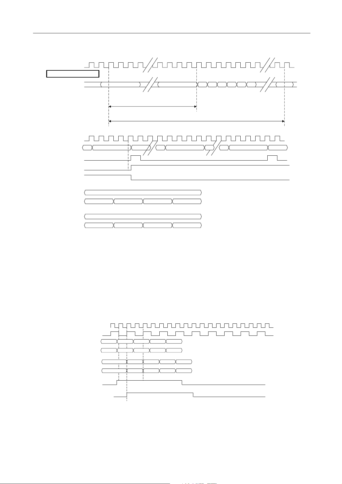
The figure below shows the input timing and the functionality of the NAPIPDL and NAPIPPH
parameter in case of CCIR 656 and 4:2:2 parallel data input format for one example. The signals
HINint, YINint and UVint are the internal available sampled input signals.
Input timing
CLK1
HIN
HINint
CCIR 656 interface
YIN
YINint
UVINint
4:2:2 interface
YIN
UVIN
YINint
UVINint
(NAPIPDL* 4 + NAPIPPH + 7) * Tclk1
=(0 * 4 + 2 + 7) * Tclk1 = 9 Tclk1 (e.g.)
(NAPIPDL* 4 + NAPIPPH + 7) * Tclk1
=(0 * 4 + 3 + 7) * Tclk1 = 10 Tclk1 (e.g.)
u0 y0 v0 y1 u2 y2 v2 y3xxx
y0 y1 y2 y3xxx
u0 v0 u2 v2xxx
u0 v0
y0
u0 v0 u2 v2
y0 y1 y3 y4
u0 v0 u2 v2
u2
y1
y2
u4 y4
v2y3u4
y4
u4
ifc01
Micronas 15 Preliminary Data Sheet
Page 16
SDA 9401
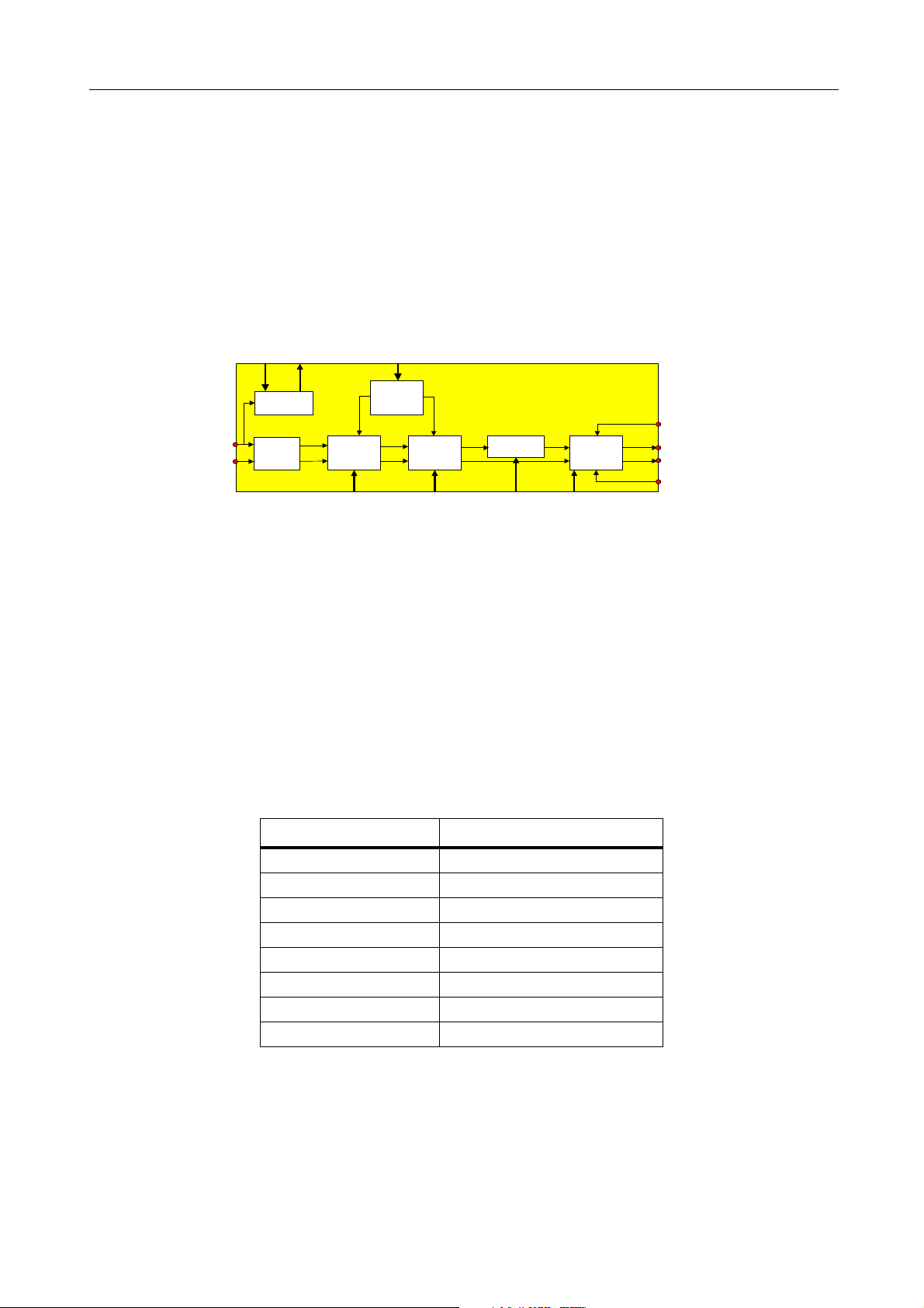
6.3 Low data rate processing
The next figure shows the block diagram of the low data rate processing block. The input signal can
be vertically and horizontally compressed by a limited number of factors. In case of multipicture
mode the internal Multipicture controller will use both compression blocks to control the different
modes. Furthermore the input signal can be processed by different noise reduction algorithms to
reduce the noise in the signal. The noise measurement block determines the noise level of the input
signal.
Block diagram of low data rate processing
MULTIPIC, PICPOS, YBORDER,
NMLINE, NMALG NOISEME
UBORDER, VBORDER
YIN
UVIN
Noise
measurement
Line
memories
Vertical
compression
VDECON,
VCSNRON
Multipicture
controller
Horizontal
compression
HDECON,
HCSNRON
Spatial noise
reduction
SNRON NRON
Temporal
noise
reduction
bdldr01
Y from Memory
Y to Memory
UV to Memory
UV from Memory
The different blocks and the corresponding parameters will be described now in more detail.
6.3.1 Vertical compression
The vertical compression compresses the incoming signal vertically by a constant factor given by
the parameter VDECON. For the Y and UV signal different filter characteristics are used. The
vertical compression can be switched off. For the multipicture modes the factors VDECON 2, 3 and
4 are necessary. Different filter characteristics are used for the factors 3 and 4. High quality vertical
compression for double window applications is possible, because the filter characteristic is
optimized for the factor 1.5.
The table below shows the relation between the parameter VDECON and the compression factor.
Input write parameter: VDECON
VDECON (1Ch)
0
1
2
3
4
5
6
7
Vertical compression off
Factor 1.25
Factor 1.5
Factor 1.75
Factor 2.0
Factor 3.0
Factor 4.0
not defined
Inside the SDA 9401 the number of active lines per field depends on the chosen vertical
compression factor VDECON (see also
chapter Output sync controller (OSC) on page 29).
Micronas 16 Preliminary Data Sheet
Page 17

SDA 9401
6.3.2 Horizontal compression
The horizontal compression compresses the incoming signal horizontally by a constant factor. For
the Y and UV signal the same filter characteristics are used. The horizontal compression can be
switched off.
The table below shows the relation between the parameter HDECON and the compression factor.
Input write parameter: HDECON
HDECON (1Ch)
00 no horizontal compression
01 factor 2
10 factor 4
11 not defined
The APPLIP (Active Pixels Per Line Input, see also chapter Input sync controller (ISC) on page 9)
value defines the length of an active line. Inside the SDA 9401 the number of active pixels per line is
APPL (Active Pixels Per Line) and its value depends on the chosen horizontal compression factor
HDECON. The table below explains the connection between APPL and APPLIP (see also
chapter
Output sync controller (OSC) on page 29).
Connection between APPL and APPLIP
Mode APPL
no horizontal compression (HDECON = ’00’) APPLIP
horizontal compression, Factor 2 (HDECON = ’01’) (APPLIP + 1) / 2
horizontal compression, Factor 4 (HDECON = ’10’) (APPLIP + 3) / 4
MULTIPIC > ’0’ (dominant, see also
chapter Multipicture display on
page 18)
45
Micronas 17 Preliminary Data Sheet
Page 18
SDA 9401
6.3.3 Multipicture display
The figures below show the different “multi picture modes” as they are represented on the display.
Fourfold multi picture
PICPOS=0 PICPOS=1
PICPOS=3PICPOS=2
Twelvefold multi picture
PICPOS=0
PICPOS=4
PICPOS=8 PICPOS=9 PICPOS=10 PICPOS=11
Sixteenfold multi picture
PICPOS=1 PICPOS=2 PICPOS=3
PICPOS=7PICPOS=6PICPOS=5
PICPOS =0 PICPOS =1 PICPOS=2 PI CPOS =3
PIC P O S= 6PI CP OS = 5PICPOS=4
PI C P OS = 7
PICPOS =8 PICPOS =9 PIC POS=10
PI C P OS = 11
PI C P OS = 15PI C PO S =14PIC P OS = 13PICPOS=12
Micronas 18 Preliminary Data Sheet
Page 19
SDA 9401
The three different “multi picture modes” can be selected by the parameter MULTIPIC. MULTIPIC=0
defines normal operation without compression. The table below explains the performed
compressions depending on the “multi picture mode” and the corresponding aspect ratio of the
display.
Input write parameter: MULTIPIC
MULTIPIC (1Bh) Horizontal compression Vertical compression Aspect ratio of the display
00 (Multi Picture Off) normal operation, no compression
01 (fourfold) 2 : 1
10 (twelvefold) 4 : 1 3 : 1
11 (sixteenfold) 4 : 1 4 : 1
To get a “multi picture display” the following executions must be performed:
Entering a “multi picture mode” is defined by transmitting a value MULTIPIC>0. This value of
MULTIPIC must not be equal to the previous value of MULTIPIC. During the following two fields the
memory will be completely filled with a constant colour defined by the parameters YBORDER,
UBORDER, VBORDER. This colour is identical to the background and the borders of the multi
picture display. The same procedure is performed when the “multi picture mode” changes from a
value MULTIPIC>0 to another value MULTIPIC>0. Beginning with the following field the
compressed input picture is written at the position PICPOS addressed via I²C-bus. The user has to
address all possible positions PICPOS one after the other to build a complete multi picture display.
In sequence, the background colour is replaced by the small pictures. The not overwritten areas of
the background colour form the borders of the multi picture display.
The pictures can be taken from the same source (’Shots of a Sequence’) or from different sources
(’Tuner Scanning’). The actual addressed picture is moving until “Freeze mode” is activated.
Before entering “multi picture mode” the “H-and-V-freerunning mode” (see also
2 : 1 4 : 3
16 : 9
4 : 3
chapter Output sync
controller (OSC) on page 29) should be activated via the I²C bus bits HOUTFR and VOUTFR,
especially when “Tuner Scanning” will be performed. The “H-and-V-freerunning mode” avoids
synchronization problems of the display during changing the tuner channel.
The values of ALPFIP (Active Lines Per Field Input, see also
page 9), and ALPFOP (Active Lines Per Field Output, see also
on page 29) must be set to 144 or 121, respectively. Only these standard signals
(OSC)
corresponding to PAL and NTSC systems are supported. A mixture of PAL and NTSC signals is
also possible.
Input write parameter
Parameter Subaddress Description
chapter Input sync controller (ISC) on
chapter Output sync controller
MULTIPIC 1Bh Defines the multi picture modes
PICPOS 1Bh Position of the picture in the multi picture mode (only
valid for MULTIPIC>0)
YBORDER 17h Y background value
UBORDER 18h U background value
VBORDER 18h V background value
Micronas 19 Preliminary Data Sheet
Page 20

SDA 9401
Parameter Subaddress Description
FREEZE
1Bh Freeze mode (frozen picture)
1: on
0: off
Interlaced conversion in multi picture mode
STOPMODE RMODE Raster Sequence Comment
0110 (AAAA mode) 0 ∼∼∼∼ (100/120 Hz)
The borders are fixed to a width of 16 pixels in horizontal direction. In vertical direction the border
widths are also fixed, the number of lines, however, depends on the TV standard of the input and
the display.
fixed
Micronas 20 Preliminary Data Sheet
Page 21
SDA 9401
6.3.4 Noise reduction
The figure below shows a block diagram of the spatial and temporal motion adaptive noise
reduction (first order IIR filter). The spatial noise reduction of the luminance differs from the spatial
noise reduction of the chrominance. The structure of the temporal motion adaptive noise reduction
is the same for the luminance as for the chrominance signal.
Block diagram of noise reduction
SNRON
YR
YIN
TNRCLY,
TNRHOY,
TNRKOY,
TNRVAY,
TNRFIY,
NRON
TNRCLC,
TNRHOC,
TNRKOC,
TNRVAC,
TNRFIC,
NRON
UVIN
Spatial
noise
reduction
Spatial
noise
reduction
VCSNRON,
HCSNRON
YSNR
DUV
UVSNR
DY
Motion
detector
Motion
detector
UV1
KY
KUV
01
TNRSEL
Field
delay
Field
delay
nr01
6.3.4.1 Spatial noise reduction
Normally a spatial noise reduction reduces the resolution due to the low pass characteristic of the
used filter. Therefore the spatial noise reduction of the SDA 9401 works adaptive on the picture
content. The low pass filter process is only executed on a homogeneous area. That’s why an edge
detection controls the low pass filter process and depending on the result of the edge detection the
pixels for the low pass filter are chosen. The next figure shows a block diagram of the spatial noise
reduction. For the UV signal only a simple spatial noise reduction algorithm (vertical and/or
horizontal low pass filtering) is implemented.
Micronas 21 Preliminary Data Sheet
Page 22

SDA 9401
Block diagram of spatial noise reduction
SNRON
YIN
UVIN
Input write parameter
Parameter Subaddress Description
SNRON
1: on
0: off
LP
0
1
1
0
HCSNRON
LM
LM
LM
LM
LP
Edge
detection
1
LP
0
VCSNRON
1Dh Spatial noise reduction of luminance signal
YSNR
nr02
UVSNR
VCSNRON
1Dh Vertical spatial noise reduction of chrominance
1: on
0: off
HCSNRON
1Dh Horizontal spatial noise reduction of chrominance
1: on
0: off
In case of VDECON>0 or HDECON>0 or MULTIPIC>0 (see also
page 16, see also
chapter Horizontal compression on page 17, see also chapter Multipicture
chapter Vertical compression on
display on page 18) spatial noise reduction is not possible.
6.3.4.2 Motion adaptive temporal noise reduction
The equation below describes the behaviour of the temporal adaptive noise reduction filter. The
same equation is valid for the chrominance signal. Depending on the motion in the input signal, the
K-factor Ky (Kuv) can be adjusted between 0 (no motion) and 15 (motion) by the motion detector.
The K-factor for the chrominance filter can be either Ky (output of the luminance motion detector,
TNRSEL=0) or Kuv (output of the chrominance motion detector, TNRSEL=1).
Micronas 22 Preliminary Data Sheet
Page 23

SDA 9401
Equation for temporal noise reduction (luminance signal)
1 Ky+
YOUT
Equation for temporal noise reduction (chrominance signal)
1 K+
UVOUT
The next figure shows the motion detector in more detail. Temporal noise reduction can be switched
off by NRON (NRON=0). The parameter TNRFIY/C switches between a fixed noise reduction Kfactor TNRVAY/C (TNRFIY/C=0) or a motion adaptive noise reduction K-factor (TNRFIY/C=1).
Block diagram of motion detector
-------------
16
----------------
16
YSNR YR–ΘΡYR+=
UVSNR UV1–ΘΡUV1 K;+ Ky Kuv;ΘΡ==
TNRCLY/C+1
TNRKOY/C+1
TNRFIY/C
NRON
Motion
LUT
TNRHOY/C
0
TNRVAY/C
1
MUX
0
1
Ky/uv
MUX
0
15
nr01
DY/UV
Motion
detection
In case of adaptive noise reduction the K-factor depends on the detected “Motion” (see figure
above). The “Motion”-Ky/Kuv characteristic curve (LUT) is fixed inside the SDA 9401, but the
characteristic curve can be changed by two parameters: TNRHOY/C and TNRKOY/C. TNRHOY/C
shifts the curve horizontally and TNRKOY/C shifts the curve vertically. For a fixed characteristic
curve, the sensitivity of the motion detector is adjustable by TNRCLY/C.
LUT for motion detection I
TNRKOY/C=7
Ky/Kuv
15
10
TNRKOY/C
TNRHOY/C=0
TNRKOY/C=-1
TNRHOY/C=0
TNRKOY/C=-8
5
51015202530
TNRHOY/C=0
Motion
nr02
Micronas 23 Preliminary Data Sheet
Page 24

SDA 9401
LUT for motion detection II
Ky/Kuv
15
10
5
TNRKOY/C=-1
TNRHOY/C=15
TNRKOY/C=-1
TNRHOY/C=0
TNRHOY/C
TNRKOY/C=-1
TNRHOY/C=-15
Motion
51015202530
nr03
Parameter TNRVAY/C
Parameter 0 (minimum value) 15 (maximum value)
TNRVAY/
C
strong noise reduction
(not motion adaptive, Ky/K=0)
no noise reduction
(not motion adaptive, Ky/K=15)
Parameter TNRHOY/C and TNRKOY/C
Parameter Range
TNRHOY/C -32, ... , 31
TNRKOY/C -8, ..., 7
Parameter TNRCLY
Parameter 0 (minimum value) 15 (maximum value)
TNRCLY/
C
maximum sensitivity for motion
-> strong noise reduction
minimum sensitivity for motion
-> weak noise reduction
Input write parameter
Parameter Subaddress Description
TNRSEL
1: separate
1Dh Switch for motion detection of temporal noise reduction
of chrominance signal
0: luminance
motion detector
Micronas 24 Preliminary Data Sheet
Page 25

SDA 9401
Parameter Subaddress Description
TNRFIY/C
21h/22h Switch for fixed K-factor value defined by TNRVAY/C
1: off
0: on
TNRVAY/C 20h Fixed K-factor for temporal noise reduction of lumi-
nance/chrominance
TNRHOY/C 21h/22h Horizontal shift of the motion detector characteristic
TNRKOY/C 1Fh Vertical shift of the motion detector characteristic
TNRCLY/C 1Eh Classification of temporal noise reduction
6.3.5 Noise measurement
The noise measurement algorithm can be used to change the parameters of the temporal noise
reduction processing depending on the actual noise level of the input signal. This is done by the I²Cbus controller which reads the NOISEME value, and sends depending on this value different
parameter sets to the temporal noise reduction registers of the SDA 9401. The NOISEME value can
be interpreted as a linear curve from no noise (0) to strong noise (30). Value 31 indicates an
overflow status and can be handled in different ways: strong noise or measurement failed.
Two measurement algorithms are included, which can be chosen by the parameter NMALG. In case
NMALG=1 the noise is measured during the vertical blanking period in the line defined by NMLINE.
For NMALG=0 the noise is measured during the first active line. In both cases the value is
determined by averaging over several fields.
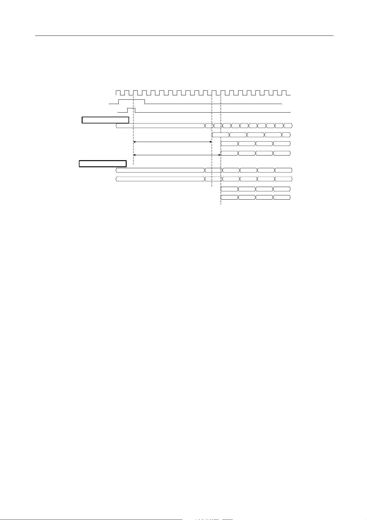
The figure below shows an example for the noise measurement. The NMLINE parameter
determines the line, which is used in the SDA 9401 for the measurement. In case of VINDEL=0 and
NMLINE=0 line 3 of the field A and line 316 of the field B is chosen. In case of VINDEL=0 and
NMLINE=3 line 6 of the field A and line 319 of the field B is chosen.
Micronas 25 Preliminary Data Sheet
Page 26

SDA 9401
Example of noise measurement
H-sync
V-sync
Field1 (A)
123456 7625624623
VINDEL=0
NMLINE=0
:
NMLINE=3
Measure
:
Field2 (B)
H-sync
V-sync
VINDEL=0
NMLINE=0
:
NMLINE=3
313-1 314-2 315-3 316-4 317-5 318-6 319-7312311310
Measure
:
PAL
Input write parameter
Parameter Subaddress Description
NMALG 1Dh Noise measurement algorithm
1: measurement during vertical blanking period (measure
line can be defined by NMLINE)
0: measurement in the first active line
Measure
NM01
Measure
NMLINE 28h Line for noise measurement (only valid for NMALG=1)
Input read parameter
Parameter Subaddress Description
NOISEME 32h Noise level of the input signal: 0 (no noise), ... , 30
(strong noise) [31 (strong noise or measurement failed)]
NMSTATUS 33h Signals a new value for NOISEME
1: a new value can be read
0: current noise measurement not finalized
(see also chapter I²C bus format on page 45)
Micronas 26 Preliminary Data Sheet
Page 27

SDA 9401
6.4 Clock concept
Input signals
Signals Pin number Description
CLK1 54 System clock 1 input
X1/CLK2 28 System clock 2 input
Output signals
Signals Pin number Description
CLKOUT 26 Clock output
The SDA 9401 supports different clock concepts. In chapter 10 (see also
chapter Application
information on page 65) a typical application of the circuit is shown. The front-end clock is
connected to CLK1 input. The CLKOUT pin is connected to the back-end and the X1/CLK2 input is
connected to a crystal oscillator. The next figure explains the different clock switches, which may be
used for the separate modes (see also page 31, “Ingenious configurations of the HOUT and VOUT
generator”).
Clock concept
CLK1
X1/CLK2
PLL1
1
PLL2
0
CLK21EN CLK11EN
CLK2_pll2
CLK1_pll1
0
1
cloco
CLKOUT
Clock concept switching matrix
CLK11EN (19h) CLK21EN (19h) CLKOUT
01CLK1
0 0 not allowed
1 X CLK2_pll2
Micronas 27 Preliminary Data Sheet
Page 28

SDA 9401
Clock Used in block
CLK1_pll1 ISC, IFC, LDR, ED, MC, LM, I²C
CLK2_pll2 OSC, HDR, ED, MC, LM, OFC
Input write parameter
Parameter Subaddress Description
PLL1OFF
02h PLL 1 on or off
1: off
0: on
PLL1RA 09h,0Ah PLL range, only for test purposes
PLL2OFF
16h PLL 2 on or off
1: off
0: on
PLL2RA 19h PLL range, only for test purposes
CLKOUTON
16h Output of system clock
1: enabled
0: disabled
Micronas 28 Preliminary Data Sheet
Page 29

SDA 9401
6.5 Output sync controller (OSC)
Output signals
Signals Pin number Description
HOUT 60 horizontal synchronization signal (polarity
programmable, I²C bus parameter 14h
HOUTPOL, default: high active)
VOUT 61 vertical synchronization signal (polarity
programmable, I²C bus parameter 14h
VOUTPOL, default: high active)
HREF 62 horizontal active video output
INTERLACED 18 interlaced signal (can be used for AC cou-
pled deflection circuits)
The output sync controller generates horizontal and vertical synchronization signals for the scan
rate converted output signal. The figures below show the block diagram of the OSC and the existing
parameters.
Block diagram of OSC
HOUTPOL, HOUTFR,
APPLOP, HOUTDEL,
NAPOP, PPLOP
HIN
VIN
OPERATION
mode
generator
STOPMODE
HOUT
generator
VOUT
generator
VOUTPOL, INTMODE,
NALOP, ALPFOP, LPFOP
WINDOW
generator
WINDVON, WINDVDR,
WINDVSP, WINDVST,
WINDHON, WINDHDR,
WINDHSP, WINDHST
HOUT
HREF
VOUT
INTERLACED
osc01
Micronas 29 Preliminary Data Sheet
Page 30

SDA 9401
Output parameter
HOUT
(PPLOP*2)*CLK2
VOUT
(NALOP+1)*2
LPFOP*4+1
Output write parameter
Parameter
[Default value]
NALOP
Subaddress Description
0Bh Not Active Line OutPut defines the number of lines from
[22]
ALPFOP
0Ch Active Lines Per Field OutPut defines the number of
[144]
(NAPOP*4)*CLK2 (APPL*16)*CLK2
(HOUTDEL*4+1)*CLK2
the V-Sync to the first active line of the output frame
active lines per output frame
(ALPFOP*4)
inpar01
(APPLOP*16)*CLK2
LPFOP
[156]
HOUTDEL
[4]
NAPOP
[0]
APPLOP
[45]
0Dh Lines Per Frame OutPut defines the number of lines per
output frame (only valid for VOUTFR=1)
0Fh HOUT DELay defines the number of pixels from the H-
Sync to the first active pixel
0Eh Not Active Pixel OutPut defines the number of not active
pixels (e.g. coloured border values)
10h Active Pixels Per Line OutPut defines the number of
pixels per line including border pixels
APPL internal Active Pixels Per Line defines the number of active
pixels (see also Horizontal compression on page 17,
APPLIP)
PPLOP
[432]
11h, 12h Pixel Per Line OutPut defines the number of pixels bet-
ween two consecutive H-Syncs (only valid for
HOUTFR=1)
Micronas 30 Preliminary Data Sheet
Page 31

SDA 9401
The next paragraphs describe the HOUT and VOUT generator in more detail. Both generators have
a so called “locked-mode” and “freerunning-mode”. Not all combinations of the modi make sense.
The table below shows ingenious configurations.
Ingenious configurations of the HOUT and VOUT generator
Mode HOUTFR VOUTFR CLK11EN CLK21EN
“H-and-V-locked” 0 0 1 1
“H-freerunning-V-locked” 1 0 1 0
“H-and-V-freerunning” 1 1 1 0
6.5.1 HOUT generator
The HOUT generator has two operation modes, which can be selected by the parameter HOUTFR.
The HOUT signal is active high (HOUTPOL=0) for 64 clock cycles (X1/CLK2). In the freerunningmode the HOUT signal is generated depending on the PPLOP parameter. In the locked-mode the
HOUT signal is locked on the incoming H-Sync signal HIN. The polarity of the HOUT signal is
programmable by the parameter HOUTPOL.
The HREF signal marks the active part of a line. The figure below shows the timing relation of the
HOUT and the HREF signal. The distance is programmable by the parameter HOUTDEL. PD
means processing delay of the internal data processing (PD=36 X1/CLK2 clocks). The length of the
active part is determined by the parameter APPLOP. If the number of the active pixels (internal
parameter APPL, see also
displayed pixels (e.g. displaying a 4:3 source on a 16:9 screen), a coloured border can be defined
using the NAPOP parameter. The border colour is defined by the parameters YBORDER,
UBORDER and VBORDER. To avoid transition artifacts of digital filters the number of active pixels
per line (parameter APPL) can be symmetrically reduced using the CAPP parameter. The figure
below shows also the internal signal ALOP, which marks the active pixels of the line.
Horizontal compression on page 17) is smaller than the number of the
Micronas 31 Preliminary Data Sheet
Page 32

SDA 9401
Timing diagram of output signals
X1/CLK2
HOUT
YOUT
UVOUT
((HOUTDEL + 1) * 4 + PD)* Tx1/clk2
HREF
YOUT
UVOUT
((HOUTDEL + 1 + NAPOP) * 4 + PD)* Tx1/clk2
ALOP
Output write parameter
Parameter Subaddress Description
HOUTFR
14h HOUT generator mode select
1: freerun
0: locked
mode
64 * Tx1/clk2
PPLOP * 2 Tx1/clk2
e.g. 432 * 2 / 27 MHz = 32 µs
y0 y1x y2 y3 y4 y5
u0 v0x u2 v2 u4 v4
APPLOP * 16 * Tx1/clk2
e.g. 45 * 16 = 720 Tx1/clk2
YB YBx YB YB y0 y1
UB VBx
UB
VB u0 v4
ym-2
um-2
YBUBYB
ym-1
vm-´2
VB
x
x
m=APPL*16
outpar01
x
x
m=APPL*16
YBORDER 17h Y border value (four MSB of the 8 bit colour)
UBORDER 18h U border value (four MSB of the 8 bit colour)
VBORDER 18h V border value (four MSB of the 8 bit colour)
CAPP
00: k = 0
01: k = 8
10h Reducing factor for the Active Pixels Per Line Value
(APPL)
Number of active pixels per line = 16 * APPL - 2*k
10: k = 16
11: k = 24
6.5.2 VOUT generator
The VOUT generator has two operation modes, which can be selected by the parameter VOUTFR.
The VOUT signal is active high (VOUTPOL=0) for two output lines. In the freerunning-mode the
VOUT signal is generated depending on the LPFOP parameter.
In the locked-mode the VOUT signal is synchronized by the incoming V-Sync signal VIN (means the
internal VIN delayed by the parameter OPDEL, see also
Input sync controller (ISC) on page 9). The
RMODE parameter (raster mode 1: progressive, 0: interlaced) determines the scan rate conversion
Micronas 32 Preliminary Data Sheet
Page 33

SDA 9401
mode. The figure below shows the two cases. If RMODE=1, then for each incoming V-sync signal
VIN an outgoing V-sync signal VOUT has to be generated (50 Hz interlaced to 50 Hz progressive
scan rate conversion). If RMODE=0, then during one incoming V-Sync signal, two VOUT pulses
have to be generated (50 Hz interlaced to 100 Hz interlaced scan rate conversion).
Examples for VOUT generation depending on parameter RMODE
VIN
RMODE=1
VOUT
RMODE=0
VOUT
The VOUT signal has a delay of two CLKOUT clocks to the HOUT signal or in case of interlaced a
delay of a half line plus two CLKOUT clocks.
Output write parameter
Parameter Subaddress Description
VOUTFR
14h VOUT generator mode select
1: freerun
0: locked
mode
RMODE
14h Raster mode
1: progressive
0: interlaced
Switching from H-and-V-freerunning to H-and-V-locked mode
In H-and-V-freerunning mode, generally, the phase of the generated synchronization raster has no
correlation to the input raster. A hard switch from the H-and-V-freerunning mode to the H-and-Vlocked mode therefore would cause visible synchronization artefacts. To avoid these problems the
SDA 9400 enlarges the line and the field lengths of the output sync signals HOUT and VOUT in a
defined procedure to enable an unvisible synchronization of the freerunning output to the input.
For vertical synchronization the maximum synchronization time is 260 ms for interlaced and 520 ms
for progressive display modes. Horizontal synchronization is performed in a maximum time of 50
ms. To get the best performance it is recommended to change at first the vertical and after the
mentioned delay times the horizontal mode from free running to locked.
Micronas 33 Preliminary Data Sheet
Page 34

SDA 9401
6.5.3 Operation mode generator
The VOUT generator determines the VOUT signal. For proper operation of the VOUT generator
information about the raster sequence is necessary. The parameter STOPMODE (Static operation
mode) defines the raster sequence and the scan rate conversion algorithm. The figure below
explains the used wording for the following explanations.
Explanations of field and display raster
FRAME/FIELD
FRAME
Content of picture
TV
DISPLAY RASTER
Display raster
odd lines
even lines
Display raster
odd lines
even lines
ϒ
FIELD A
FIELD B
Display raster
∼
fieldras01
Tube, Display raster
The interlaced input signal (e.g. 50 Hz PAL or 60 Hz NTSC) is composed of a field A (odd lines) and
a field B (even lines).
n
A
- Input signal, field A at time n,
n
B
- Input signal, field B at time n
The field information describes the picture content. The output signal, which could contain different
picture contents (e.g. field A, field B ) can be displayed with the display raster ∼ or ϒ.
n
,∼) - Output signal, field A at time n, displayed as raster ∼Ι
(A
Micronas 34 Preliminary Data Sheet
Page 35

SDA 9401
(An,ϒ) - Output signal, field A at time n, displayed as raster ϒΙ
n
((A*)
,ϒ) - Output signal, field A raster interpolated into field B at time n, displayed as raster ϒ
n Bn-1
(A
The table below describes the different scan rate conversion algorithms and the corresponding
raster sequences. The delay between the input field and the corresponding output fields depends
on the OPDEL parameter and the default value for the delay is an half input field.
The INTERLACED signal can be used for AC-coupled deflections. Depending on the parameter
INTMODE the value of this signal will be generated. The table below shows also the definition of
this signal.
Explanation of operation mode timing
,∼+ϒΦ=ϑ=Output signal, frame AB at time n, progressive
Input fields
time
Fields available in
the internal field stores
Output fields
n-1
A
, B
OPDEL lines
A
n-1
n
n-1
, A
n
b
Phase 1
a
Phase
0
B
n
n
B
n
n
c
Phase 2/0
An, B
osc02
n
Phase 3/1
n
d
Static operation modes
STOPMODE
Scan rate conversion
algorithm
Input field
A
Output
n
field a
phase 0
Output
field b
phase 1
n
Input field
B
Output
n
field c
phase 2/0
Output
n
field d
phase 3/1
RMODE
0000 not defined xxxx0
0001 AA*B*B mode I
interlaced
0010 AABB mode I
interlaced
0100 Multipicture mode IA
0101 Multipicture mode IIB
(A*)n,↑
INTMODE(3)
n
,←
A
INTMODE(0)
n
,↑
INTMODE(0)
n-1
,↑
INTMODE(1)
An,←
INTMODE(0)
An,←
INTMODE(0)
An,←
INTMODE(0)
n-1
B
,←
INTMODE(1)
Bn,↑
INTMODE(1)
Bn,↑
INTMODE(1)
An,↑
INTMODE(0)
Bn,↑
INTMODE(1)
(B*)n,←
INTMODE(2)
Bn,↑
INTMODE(1)
An,←
INTMODE(0)
Bn,←
INTMODE(1)
0
0
0
0
0110 AAAA mode An,←
INTMODE(0)
0111 BBBB mode B
n-1
INTMODE(0)
,↑
An,←
INTMODE(0)
n-1
B
,↑
INTMODE(0)
An,←
INTMODE(0)
Bn,↑
INTMODE(0)
An,←
INTMODE(0)
Bn,↑
INTMODE(0)
0
0
1000 not defined xxxx0
Micronas 35 Preliminary Data Sheet
Page 36

SDA 9401
STOPMODE
Scan rate conversion
algorithm
1001 AA*B*B mode II
interlaced
1010 AABB mode II
interlaced
Input field
A
Output
field a
phase 0
n-1
(B*)
INTMODE(2)
n-1
B
,↑
INTMODE(1)
n
,←
Output
field b
phase 1
n-1
B
,↑
INTMODE(1)
n-1
B
,↑
INTMODE(1)
n
Input field
B
Output
n
field c
phase 2/0
n+1
A
,←
INTMODE(0)
n+1
A
,←
INTMODE(0)
Output
field d
phase 3/1
n+1
(A*)
INTMODE(3)
n+1
A
,←
INTMODE(0)
n
RMODE
,↑
0
0
1011,11xxnot definedxxxx0
0000 not defined xxxx1
0001 AA* mode I pro-
gressive
(An A*n,
←Τ↑)
(B*n Bn,
←Τ↑)
1
0010 not defined xxxx1
0101 AA* mode II pro-
gressive
0111 B*B mode progres-
sive
(An A*n,
←Τ↑)
n-1
(B
n-1
B*
,
(An A*n,
←Τ↑)
(Bn B*n,
←Τ↑)
1
1
←Τ↑)
0011,0100,
not definedxxxx1
0110
1000 Test Mode (motion
adaptive mode
interlaced, DL)
An A*n ΥΙ
←Τ↑ΞΙ
←Τ↑)
B*n Bn,
a+b/
←Τ↑)
1
1xxx not defined xxxx1
The table below shows all possible display raster sequences for the different static operation modes
and the line per field value between two consecutive output V-Syncs. It is assumed, that in case of
freerunning-mode LPFOP=156 and in the locked mode the number of lines of the incoming field is
312.5.
Display raster sequence for RMODE=1 (progressive)
Display raster
sequence
1. to 2. 2. to 3. (1.)
←Τ↑ 625 625
Display raster sequence for RMODE=0 (interlaced)
Display raster
sequence
1. to 2. 2. to 3. 3. to 4. 4. to 5.(1.)
←←←← 312 313 312 313
Micronas 36 Preliminary Data Sheet
Page 37

SDA 9401
Display raster
sequence
1. to 2. 2. to 3. 3. to 4. 4. to 5.(1.)
↑↑↑↑ 313 312 313 312
←←↑↑ 312 312.5 313 312.5
↑↑←← 313 312.5 312 312.5
←Τ↑Ξ←Τ↑ΙΘtest
625.5 624.5 625.5 624.5
mode only)
Output write parameter
Parameter Subaddress Description
STOPMODE 12h Static operation modes
INTMODE 13h, 14h Free programmable INTERLACED signal for AC-cou-
pled deflection stages
6.5.4 Window generator
The figures below show the functionality of the horizontal and/or vertical window function. The
actual TV display can be overwritten with a constant value (defined by YBORDER, UBORDER,
VBORDER), which is called “closing” or the constant value can be overwritten with the actual TV
signal, which is called “opening”. For the generation some parameters exist, which will be explained
in more detail afterwards.
Examples for window feature
WINDOW
Micronas 37 Preliminary Data Sheet
Page 38

SDA 9401
The feature can be enabled by the parameter WINDHON/WINDVON. The parameter WINDHST/
WINDVST defines the status of the window (opened or closed). Closed means, that only a constant
value is displayed, opened means, that the full TV is displayed. The parameter WINDHDR/
WINDVDR defines, what can be done with the window (open the window, close the window).
Output write parameter: WINDHST/WINDVST and WINDHDR/WINDVDR
WINDHST/
WINDVST
Description
WINDHDR/
WINDVDR
Description
0 Window is closed 0 open the window
0 Window is closed 1 window remains closed
1 Window is opened 0 window remains open
1 Window is opened 1 close the window
With each enabling of the window function by the WINDHON/WINDVON parameter, the status of
the window will be as defined by the table above, that means the WINDHST/WINDVST parameter is
only once interpreted after enabling the window function. To change afterwards the status from
“window is close” to “window is open” or vice versa only the WINDHDR/WINDVDR has to be
toggled. If for example the status WINDHST/WINDVST=0 and the WINDHDR/WINDVDR=0 the
window is closed and will be open after enabling the feature by setting the parameter WINDHON/
WINDVON=1. To close the window only the parameter WINDHDR/WINDVDR has to be set to 1.
Again to open the window WINDHDR/WINDVDR has to be set to 0.
For example:
After switching on the TV set, the customer should see the window closed and afterwards the
window should be opened. Therefore the WINDHST/WINDVST has to be set to “0”, the WINDHDR/
WINDVDR has to be set to “1” and the WINDHON/WINDVON has to be set to “1”. So the customer
will see first a screen with a colour defined by the I²C parameters YBORDER, UBORDER and
VBORDER. Then the WINDHDR/WINDVDR has to be set to “0”, that means the window will be
open and the customer will see the chosen TV channel.
The speed of closing or opening the window can be defined by the parameter WINDHSP/
WINDVSP. The tables below explain the using of these parameters.
Output write parameter: WINDHSP
time to close/
open (e.g. 720
active pixel,
10ms per output
field)
windhsp
freerun
mode
locked
mode
00 pplop/256 distance/512 ~4s
01 pplop/128 distance/256 ~2s
10 pplop/64 distance/128 ~1s
Micronas 38 Preliminary Data Sheet
Page 39

SDA 9401
time to close/
open (e.g. 720
active pixel,
10ms per output
field)
windhsp
freerun
mode
locked
mode
11 pplop/32 distance/64 ~0.5s
Distance: Number of pixels in system clocks X1/CLK2 between two output H-Syncs
time to close = time(field) * number of active pixels / (distance/512)
e.g. time to close = 10 ms * 720 / (864/512) = 4,26 s
time to close = time(field) * number of active pixels / (pplop/128)
Output write parameter: WINDVSP
time to close/
open (e.g. 576
active lines,
10ms per output
field)
windvsp
freerun
mode
locked
mode
00 lpfop/128 lpfip/256 ~5s
01 lpfop/64 lpfip/128 ~2s
10 lpfop/32 lpfip/64 ~1s
11 lpfop/16 lpfip/32 ~0.5s
LPFIP: Lines per field of the input signal - amount of lines between two input V-Syncs
time to close = time(field(interlaced)/frame(progressive)) * number of active lines / (lpfip/256)
e.g. time to close = 10 ms * 576 / (312/256) = 4.7 s
time to close = time(field) * number of active lines / (lpfop/128)
Output write parameter
Parameter Subaddress Description
WINDVON
15h Vertical window feature on or off
1: on
0: off
WINDVDR
15h Direction of the vertical window feature
1: close window
0: open window
WINDVST
1: window is opened
15h Status of the vertical window feature after enabling the
window feature
0: window is closed
WINDVSP 15h Speed of the vertical window feature
Micronas 39 Preliminary Data Sheet
Page 40

SDA 9401
Parameter Subaddress Description
WINDHON
16h Horizontal window feature on or off
1: on
0: off
WINDHDR
16h Direction of the horizontal window feature
1: close window
0: open window
WINDHST
1: window is opened
16h Status of the horizontal window feature after enabling the
window feature
0: window is closed
WINDHSP 16h Speed of the horizontal window feature
FLASHON
1: on
0: off
17h Flash of the TV signal (after each output V-Sync the TV
signal or the constant background value defined by
YBORDER, UBORDER, VBORDER is displayed)
6.6 Output format conversion (OFC)
Output signals
Signals Pin number Description
YOUT0...7 7, 6, 5, 4, 3, 1, 64, 63 luminance output
UVOUT0...7 17, 16, 15, 14, 13, 12, 11, 10 chrominance output
The SDA 9401 supports at the output side only the sample frequency relations of Y : (B-Y) : (R-Y):
4:2:2. The representation of the samples of the chrominance signal is programmable as positive
dual code (unsigned, parameter TWOOUT=0) or two's complement code (TWOOUT=1, see also
I²C bus format on page 45, I²C bus parameter 17h).
Output data format
Data
Pin
YIN7 Y
YIN6 Y
YIN5 Y
YIN4 Y
YIN3 Y
YIN2 Y
YIN1 Y
YIN0 Y
4:2:2 Parallel
07
06
05
04
03
02
01
00
Y
Y
Y
Y
Y
Y
Y
Y
17
16
15
14
13
12
11
10
Micronas 40 Preliminary Data Sheet
Page 41

SDA 9401
Data
4:2:2 Parallel
Pin
UVIN7 U
UVIN6 U
UVIN5 U
UVIN4 U
UVIN3 U
UVIN2 U
UVIN1 U
UVIN0 U
07
06
05
04
03
02
01
00
V
07
V
06
V
05
V
04
V
03
V
02
V
01
V
00
X ab: X: signal component a: sample number b: bit number
6.7 High data rate processing (HDR)
The output signal can be vertically expanded. The expansion as well as the different scan rate
conversion algorithms are processed in the HDR block. For the vertical expansion line memories
are used. If the operation frequency X1/CLK2 is higher than 27 MHz plus 10%, the line memories
will not work correctly any more. In this case only simple processing will be possible. Simple
processing means, that the vertical expansion must be disabled.
The table below defines the internal expansion factor ZOOM depending on the RMODE and
VERINT parameter.
Output write parameter: VERINT
VERINT RMODE ZOOM
I²C-bus
0 2*(VERINT+1)
parameter
I²C-bus
1 (VERINT+1)
parameter
The reachable expansion factors are listed in the table below in case of VDECON=0 and
VDECON=2 (vertical compression of the input signal with factor 1.0 and 1.5).
Micronas 41 Preliminary Data Sheet
Page 42

SDA 9401
Examples of reachable expansion factors
100/120 Hz
interlaced
RMODE=0
VERINT ZOOM ZOOM VDECON=0 VDECON=2
63 128 64 1.00 0.75
62 126 63 1.02 0.76
61 124 62 1.03 0.77
60 122 61 1.05 0.79
59 120 60 1.07 0.80
58 118 59 1.08 0.81
57 116 58 1.10 0.83
56 114 57 1.12 0.84
55 112 56 1.14 0.86
54 110 55 1.16 0.87
53 108 54 1.19 0.89
52 106 53 1.21 0.91
51 104 52 1.23 0.92
50 102 51 1.25 0.94
49 100 50 1.28 0.96
48 98 49 1.31 0.98
47 96 48 1.33 1.00
46 94 47 1.36 1.02
45 92 46 1.39 1.04
44 90 45 1.42 1.07
43 88 44 1.45 1.09
42 86 43 1.49 1.12
41 84 42 1.52 1.14
40 82 41 1.56 1.17
39 80 40 1.60 1.20
38 78 39 1.64 1.23
37 76 38 1.68 1.26
36 74 37 1.73 1.30
35 72 36 1.78 1.33
34 70 35 1.83 1.37
33 68 34 1.88 1.41
32 66 33 1.94 1.45
31 64 32 2.00 1.50
30 62 31 2.06 1.55
29 60 30 2.13 1.60
28 58 29 2.21 1.66
27 56 28 2.29 1.71
50/60 Hz
progressive
RMODE=1
real vertical
expansion
factor
real vertical
expansion
factor
Micronas 42 Preliminary Data Sheet
Page 43

SDA 9401
100/120 Hz
interlaced
RMODE=0
VERINT ZOOM ZOOM VDECON=0 VDECON=2
26 54 27 2.37 1.78
25 52 26 2.46 1.85
24 50 25 2.56 1.92
23 48 24 2.67 2.00
22 46 23 2.78 2.09
21 44 22 2.91 2.18
20 42 21 3.05 2.29
19 40 20 3.20 2.40
18 38 19 3.37 2.53
17 36 18 3.56 2.67
16 34 17 3.76 2.82
15 32 16 4.00 3.00
14 30 15 4.27 3.20
13 28 14 4.57 3.43
12 26 13 4.92 3.69
11 24 12 5.33 4.00
10 22 11 5.82 4.36
920106.404.80
8 18 9 7.11 5.33
7 16 8 8.00 6.00
6 14 7 9.14 6.86
5 12 6 10.67 8.00
4 10 5 12.80 9.60
3 8 4 16.00 12.00
2 6 3 21.33 16.00
1 4 2 32.00 24.00
0 2 1 64.00 48.00
50/60 Hz
progressive
RMODE=1
real vertical
expansion
factor
real vertical
expansion
factor
The parameter VPAN can be used to select the start line of the expansion. To expand the upper
part of the incoming signal with the factor 2.0, VPAN should be set to zero. To expand the lower
part, VPAN should be equal to 144. That means in case of VPAN=0 the first used line is line 1 and
in case of VPAN=144 the first used line is line 144.
Dependent on the parameter VERINT a certain number of input lines of the input field is required.
Therefore not all VPAN values are allowed. The formula below can be used to calculate the
maximum allowed VPAN value depending on the chosen VERINT value.
Calculation of maximum VPAN value
VERINT 1+ΘΡ
VPANmax 2 ALPFOP 1
=
------------------------------------
–
64
Micronas 43 Preliminary Data Sheet
Page 44

SDA 9401
Floor symbol means: take only integer part of x
x
Output write parameter
Parameter Subaddress Description
VERINT 13h Vertical expansion factor
VPAN 1Ah Vertical adjustment of the output picture
Micronas 44 Preliminary Data Sheet
Page 45

SDA 9401
6.8 I²C bus
6.8.1 I²C bus slave address
Write Adress: BCh
10111100
Read Adress: BDh
10111101
6.8.2 I²C bus format
The SDA 9401 I²C bus interface acts as a slave receiver and a slave transmitter and provides two
different access modes (write, read). All modes run with a subaddress auto increment. The interface
supports the normal 100 kHz transmission speed as well as the high speed 400 kHz transmission.
write:
S10111100A Subaddress A Data Byte A
S: Start condition
A: Acknowledge
P: Stop condition
NA: Not Acknowledge
read:
*****
AP
S10111100A Subaddress AS10111101A Data Byte A
Data Byte NA P
The transmitted data are internally stored in registers. The master has to write a don’t care byte to
the subaddress FFh (store command) to make the register values available for the SDA 9401. To
have a defined time step, where the data will be available, the data are made valid with the incoming
V-sync VIN or with the next OPSTART pulse, which is an internal signal and indicates the start of a
new output cycle. The subaddresses, where the data are made valid with the VIN signal are
indicated in the overview of the subaddresses with „VI“, where the data are made valid with the
OPSTART are indicated with „OS“. The I²C parameter VISTATUS and OSSTATUS (subaddress
33h) reflect the state of the register values. If these bits are read as ’0’, then the store command was
sent, but the data aren’t made available yet. If these bits are ’1’ then the data were made valid and a
new write or read cycle can start. The bits VISTATUS and OSSTATUS may be checked before
writing or reading new data, otherwise data can be lost by overwriting.
Furthermore the bit NMSTATUS (status of noise measurement: NOISEME). NMSTATUS signalizes
a new value for NOISEME. So if NMSTATUS is read as ’0’ the current noise measurement has not
Micronas 45 Preliminary Data Sheet
Page 46

SDA 9401
been finalized. If the NMSTATUS is read as ’1’ a new noise measurement value can be read.
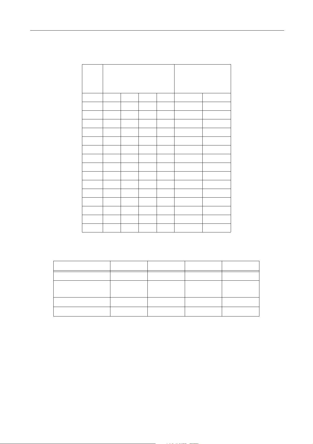
After switching on the IC, all bits of the SDA 9401 are set to defined states. Particularly :
Subaddress Default value R/W
Tak e
over
Subaddress Default value R/W
00 11h W VI 15 00h W OS
01 00h W VI 16 04h W OS
02 50h W VI 17 14h W OS
03 90h W VI 18 88h W OS
04 00h W VI 19 0Ch W OS
05 B4h W VI 1A 00h W OS
06 AAh W VI 1B 00h W VI
07 00h W VI 1C 01h W VI
08 00h W VI 1D 03h W VI
09 00h W VI 1E FFh W VI
0A 00h W VI 1F 00h W VI
0B 16h W OS 20 FFh W VI
0C 90h W OS 21 02h W VI
0D 9Ch W OS 22 02h W VI
0E 00h W OS 23...27 not used
Take
over
0F 04h W OS 28 22h W VI
10 B4h W OS 29...31 not used
11 B0h W OS 32 R
12 90h W OS 33 R
13 3Fh W OS 34...FE not used
14 00h W OS FF W
R/W: R - Read Register; W - Write Register; R/W - Read and Write Register;
Take over: VI - take over with VIN; OS- take over with OPSTART
Reading the “Read only” register 32h must be followed by reading the “Read only” register 33h.
Micronas 46 Preliminary Data Sheet
Page 47

SDA 9401
6.8.3 I²C bus commands
Subadd.
(Hex.)
00
01
02
03
04
05
06
07
08
09
0A
0B
0C
0D
0E
0F
10
11
12
13
14
15
Data Byte
D7 D6 D5 D4 D3 D2 D1 D0
FORMAT1
ISC/IFC
VINDEL5
ISC
NALIP5
ISC
ALPFIP7
ISC
NAPIPDL7
ISC
APPLIP5
ISC
OPDEL7
ISC
VERWIDTH7
ISC
VERPOS7
ISC
HORWIDTH5
ISC
HORPOS5
ISC
NALOP7
OSC
ALPFOP7
OSC
LPFOP7
OSC
NAPOP7
OSC
HOUTDEL7
OSC
APPLOP5
OSC
PPLOP7
OSC
PPLOP8
OSC
INTMODE3
OSC
INTMODE1
OSC
WINDVON
OSC
FORMAT0
ISC/IFC
VINDEL4
ISC
NALIP4
ISC
ALPFIP6
ISC
NAPIPDL6
ISC
APPLIP4
ISC
OPDEL6
ISC
VERWIDTH6
ISC
VERPOS6
ISC
HORWIDTH4
ISC
HORPOS4
ISC
NALOP6
OSC
ALPFOP6
OSC
LPFOP6
OSC
NAPOP6
OSC
HOUTDEL6
OSC
APPLOP4
OSC
PPLOP6
OSC
STOPMODE3
OSC
INTMODE2
OSC
INTMODE0
OSC
WINDVDR
OSC
FIEINV
ISC
VINDEL3
ISC
NALIP3
ISC
ALPFIP5
ISC
NAPIPDL5
ISC
APPLIP3
ISC
OPDEL5
ISC
VERWIDTH5
ISC
VERPOS5
ISC
HORWIDTH3
ISC
HORPOS3
ISC
NALOP5
OSC
ALPFOP5
OSC
LPFOP5
OSC
NAPOP5
OSC
HOUTDEL5
OSC
APPLOP3
OSC
PPLOP5
OSC
STOPMODE2
OSC
VERINT5
OSC
0
WINDVST
OSC
VCRMODE
ISC
VINDEL2
ISC
NALIP2
ISC
ALPFIP4
ISC
NAPIPDL4
ISC
APPLIP2
ISC
OPDEL4
ISC
VERWIDT4
ISC
VERPOS4
ISC
HORWIDTH2
ISC
HORPOS2
ISC
NALOP4
OSC
ALPFOP4
OSC
LPFOP4
OSC
NAPOP4
OSC
HOUTDEL4
OSC
APPLOP2
OSC
PPLOP4
OSC
STOPMODE1
OSC
VERINT4
OSC
RMODE
OSC
WINDVSP1
OSC
PIMODE
ISC
VINDEL1
ISC
NALIP1
ISC
ALPFIP3
ISC
NAPIPDL3
ISC
APPLIP1
ISC
OPDEL3
ISC
VERWIDTH3
ISC
VERPOS3
ISC
HORWIDTH1
ISC
HORPOS1
ISC
NALOP3
OSC
ALPFOP3
OSC
LPFOP3
OSC
NAPOP3
OSC
HOUTDEL3
OSC
APPLOP1
OSC
PPLOP3
OSC
STOPMODE0
OSC
VERINT3
OSC
VOUTFR
OSC
WINDVSP0
OSC
NAPIPPH1
ISC
VINDEL0
ISC
NALIP0
ISC
ALPFIP2
ISC
NAPIPDL2
ISC
APPLIP0
ISC
OPDEL2
ISC
VERWIDTH2
ISC
VERPOS2
ISC
HORWIDT0
ISC
HORPOS0
ISC
NALOP2
OSC
ALPFOP2
OSC
LPFOP2
OSC
NAPOP2
OSC
HOUTDEL2
OSC
APPLOP0
OSC
PPLOP2
OSC
000
VERINT2
OSC
HOUTFR
OSC
000
NAPIPPH0
ISC
VINPOL
ISC
PLL1OFF
PLL1
ALPFIP1
ISC
NAPIPDL1
ISC
xx
OPDEL1
ISC
VERWIDTH1
ISC
VERPOS1
ISC
PLL1RA1
PLL1
PLL1RA3
PLL1
NALOP1
OSC
ALPFOP1
OSC
LPFOP1
OSC
NAPOP1
OSC
HOUTDEL1
OSC
CAPP1
OSC
PPLOP1
OSC
VERINT1
OSC
VOUTPOL
OSC
TWOIN
ISC/IFC
HINPOL
ISC
REFRESH
MC
ALPFIP0
ISC
NAPIPDL0
ISC
OPDEL0
ISC
VERWIDTH0
ISC
VERPOS0
ISC
PLL1RA0
PLL1
PLL1RA2
PLL1
NALOP0
OSC
ALPFOP0
OSC
LPFOP0
OSC
NAPOP0
OSC
HOUTDEL0
OSC
CAPP0
OSC
PPLOP0
OSC
VERINT0
OSC
HOUTPOL
OSC
Micronas 47 Preliminary Data Sheet
Page 48

SDA 9401
16
17
18
19
1A
1B
1C
1D
1E
1F
20
21
22
28
32
33
WINDHON
OSC
YBORDER3
OFC/LDR
UBORDER3
OFC/LDR
PLL2RA3
PLL2
VPAN7
MC
MULTIPIC1
LDR/ISC
VDECON2
LDR
NRON
LDR/MC
TNRCLY3
LDR
TNRKOY3
LDR
TNRVAY3
LDR
TNRHOY5
LDR
TNRHOC5
LDR
NMLINE4
LDR
NOISME4
LDR
xxx
WINDHDR
OSC
YBORDER2
OFC/LDR
UBORDER2
OFC/LDR
PLL2RA2
PLL2
VPAN6
MC
MULTIPIC0
LDR/ISC
VDECON1
LDR
SNRON
LDR
TNRCLY2
LDR
TNRKOY2
LDR
TNRVAY2
LDR
TNRHOY4
LDR
TNRHOC4
LDR
NMLINE3
LDR
NOISME3
LDR
WINDHST
OSC
YBORDER1
OFC/LDR
UBORDER1
OFC/LDR
PLL2RA1
PLL2
VPAN5
MC
PICPOS3
LDR/MC
VDECON0
LDR
VCSNRON
LDR
TNRCLY1
LDR
TNRKOY1
LDR
TNRVAY1
LDR
TNRHOY3
LDR
TNRHOC3
LDR
NMLINE2
LDR
NOISEME2
LDR
WINDHSP1
OSC
YBORDER0
OFC/LDR
UBORDER0
OFC/LDR
PLL2RA0
PLL2
VPAN4
MC
PICPOS2
LDR/MC
HDECON1
LDR/ISC
HCSNRON
LDR
TNRCLY0
LDR
TNRKOY0
LDR
TNRVAY0
LDR
TNRHOY2
LDR
TNRHOC2
LDR
NMLINE1
LDR
NOISEME1
LDR
TVMODE
LDR
WINDHSP0
OSC
FLASHON
OFC
VBORDER3
OFC/LDR
CLK21EN
PLL2
VPAN3
MC
PICPOS1
LDR/MC
HDECON0
LDR/ISC
00
TNRCLC3
LDR
TNRKOC3
LDR
TNRVAC3
LDR
TNRHOY1
LDR
TNRHOC1
LDR
NMLINE0
LDR
NOISEME0
LDR
VISTATUS OSSTATUS x NMSTATUS
CLKOUTON
PLL2
TWOOUT
OFC
VBORDER2
OFC/LDR
CLK11EN
PLL2
VPAN2
MC
PICPOS0
LDR/MC
001
TNRCLC2
LDR
TNRKOC2
LDR
TNRVAC2
LDR
TNRHOY0
LDR
TNRHOC0
LDR
01x
VERSION2 VERSION1 VERSION0
PLL2OFF
PLL2
00
VBORDER1
OFC/LDR
00
VPAN1
MC
FREEZE
MC
TNRSEL
LDR
TNRCLC1
LDR
TNRKOC1
LDR
TNRVAC1
LDR
TNRFIY
LDR
TNRFIC
LDR
x
VBORDER0
OFC/LDR
VPAN0
MC
0
NMALG
LDR
TNRCLC0
LDR
TNRKOC0
LDR
TNRVAC0
LDR
0
0
FF
xxxxxxxx
x = don’t care
ISC - Input sync controller block
IFC - Input format conversion block
OSC - Output sync controller block
OFC - Output format conversion block
LDR - Low data rate block
HDR - High data rate block
MC - Memory controller
PLL1 - Clock doubling block 1
PLL2 - Clock doubling block 2
Micronas 48 Preliminary Data Sheet
Page 49

SDA 9401
6.8.4 Detailed description
Default values are underlined.
Subaddress 00
Bit Name Function
Input format:
11: full CCIR 656
D7...D6 FORMAT
D5 FIEINV
D4 VCRMODE
D3 PIMODE
NAPIPPH
D2...D1
(LSBs of
NAPLIP)
10: CCIR 656 only data, H- and V-sync according CCIR656
01: CCIR 656 only data, H- and V-sync according PAL/NTSC
00: 4:2:2
Field polarity inversion:
1: Field A=1, Field B=0
0: Field A=0, Field B=1
Input filtering of the incoming field signal:
1: on
0: off
Picture insert mode (see VERWIDTH, VERPOS, HORWIDTH, HORPOS):
1: on
0: off
Number of not active pixels from external HIN to the input data in system
clocks of CLK1:
Number(HIN to input data) = (NAPIPDL*4+NAPIPPH+8) [NAPIPPH = 0
]
Chrominance input format:
D0 TWOIN
Bit Name Function
D7...D2 VINDEL
D1 VINPOL
D0 HINPOL
1: 2’s complement input (-128...127)
0: unsigned input (0...255)
inside the SDA 9401 the data are always processed as unsigned data
Subaddress 01
VIN input delay:
Delay(VIN to internal V-sync) = (128 * VINDEL + 1)*Tclk1 [VINDEL = 0
VIN polarity:
1: low active
0: high active
HIN polarity:
1: low active
0: high active
]
Micronas 49 Preliminary Data Sheet
Page 50

SDA 9401
Subaddress 02
Bit Name Function
D7...D2 NALIP
D1 PLL1OFF
D0 REFRESH
Bit Name Function
D7...D0 ALPFIP
Bit Name Function
Number of not active lines per field in the input data stream:
Not active lines = NALIP+3 [NALIP= 20
PLL1 switch:
1: off
0: on
Internal refresh:
1: on
0: off
Subaddress 03
Number of active lines per field in the input data stream:
Active lines = ALPFIP * 2 [ALPFIP=144
Subaddress 04
]
]
NAPIPDL
D7...D0
Bit Name Function
D7...D2 APPLIP
D1...D0 x
(MSBs of
NAPLIP)
Number of not active pixels from HIN to the input data in system clocks of
CLK1:
Number(HIN to input data) = (4 * NAPIPDL + NAPIPPH + 8) [NAPIPDL=
0]
Subaddress 05
Number of active pixels per line in the input data stream in system clocks
of CLK1:
Active pixels = APPLIP*32 [APPLIP = 45
Inside the SDA 9401 the number of active pixels per line is APPL*32, with
APPL =
APPLIP, MULITPIC = 0 and HDECON = 0
(APPLIP + 1)/2, MULTIPIC = 0 and HDECON = 1
(APPLIP + 3)/4, MULTIPIC = 0 and HDECON = 2
45, MULTIPIC > 0
x
]
Micronas 50 Preliminary Data Sheet
Page 51

SDA 9401
Subaddress 06
Bit Name Function
D7...D0 OPDEL
Bit Name Function
D7...D0 VERWIDTH
Bit Name Function
D7...D0 VERPOS
Output processing delay (in number of lines):
Delay(VIN to VOUT) = (OPDEL + 1) * Tline [OPDEL = 170
Subaddress 07
Vertical width of inserted picture in input lines:
Vertical width = (2 * VERWIDTH) [VERWIDTH = 0
Subaddress 08
Vertical position of inserted picture in input lines:
Vertical position = (2 * VERPOS) + NALIP + 3 [VERPOS = 0
Subaddress 09
]
]
]
Bit Name Function
D7...D2 HORWIDTH
D1...D0 PLL1RA(1...0)
Bit Name Function
D7...D2 HORPOS
D1...D0 PLL1RA(3...2)
Horizontal width of inserted picture in system clocks of CLK1:
Horizontal width = (32 * HORWIDTH) [HORWIDTH = 0
PLL1 range, only for test purposes [PPL1RA=0
Subaddress 0A
Horizontal position of inserted picture in system clocks of CLK1:
Horizontal position = (32 * HORPOS) + (4 * NAPIPDL + NAPIPPH + 8)
[HORPOS = 0
PLL1 range, only for test purposes [PPL1RA=0
]
]
]
]
Micronas 51 Preliminary Data Sheet
Page 52

SDA 9401
Subaddress 0B
Bit Name Function
D7...D0 NALOP
Bit Name Function
D7...D0 ALPFOP
Bit Name Function
D7...D0 LPFOP
Number of not active lines per frame in the output data stream:
Not active lines = 2 * (NALOP + 1) [NALOP= 22]
Subaddress 0C
Number of active lines per output frame:
Active lines = 4 * ALPFOP [ALPFOP= 144
Subaddress 0D
Number of lines per output frame (only valid for VOUTFR=1):
Number of lines = 4 * LPFOP + 1 [LPFOP = 156
Subaddress 0E
]
]
Bit Name Function
Number of not active pixels (coloured border values) from external HREF
D7...D0 NAPOP
Bit Name Function
D7...D0 HOUTDEL
to the first active pixel of the output data stream in system clocks of X1/
CLK2:
Distance(HREF to output data) = (4 * NAPOP) [NAPOP = 0
Subaddress 0F
HOUT delay:
Delay(HOUT to HREF) = (4 * (HOUTDEL + 1) + 36) *Tx1/clk2 [HOUTDEL
= 4]
]
Micronas 52 Preliminary Data Sheet
Page 53

SDA 9401
Subaddress 10
Bit Name Function
Number of active pixels per line (including coloured border values and
D7...D2 APPLOP
D1...D0 CAPP
data) in the output data stream in system clocks of X1/CLK2 (length of
HREF):
Active pixels = 16 * APPLOP [APPLOP = 45
Reduces the active pixels per line (APPL) at the output side:
Active pixels per line at the output side in system clocks of X1/CLK2
= 16 * APPL - 2 * k
k =
24: CAPP = 11
16: CAPP = 10
8: CAPP = 01
0: CAPP = 00
]
Subaddress 11
Bit Name Function
Number of pixels between two output H-syncs HOUT (only valid for
D7...D0 PPLOP(7...0)
Bit Name Function
D7 PPLOP(8)
D6...D3 STOPMODE
D2...D0 should be set to 000
HOUTFR=1) in system clocks of X1/CLK2 (Bit 7 to 0):
Number of pixels = 2 * PPLOP [PPLOP = 432
Subaddress 12
Number of pixels between two output H-syncs HOUT (only valid for
HOUTFR=1) in system clocks of X1/CLK2 (Bit 8):
Number of pixels = 2 * PPLOP [PPLOP = 432
Static operation modes (see also
34):
0010: AABB mode I interlaced
Operation mode generator on page
]
]
Subaddress 13
Bit Name Function
D7...D6 INTMODE(3...2)
Free programmable INTERLACED signal for AC coupled deflection
stages (Bit 3 and Bit 2) [INTMODE3...2 = 0
]
Micronas 53 Preliminary Data Sheet
Page 54

SDA 9401
Subaddress 13
Bit Name Function
Vertical expansion factor (see also
on page 41):
63: no vertical expansion
D5...D0 VERINT
Bit Name Function
D7...D6 INTMODE(1...0)
D5
D4 RMODE
D3 VOUTFR
D2 HOUTFR
D1 VOUTPOL
D0 HOUTPOL
:
47: vertical expansion with factor 1.5
:
31: vertical expansion with factor 2
:
Subaddress 14
Free programmable INTERLACED signal for AC coupled deflection
stages (Bit 1 and Bit 0) [INTMODE1...0 = 0
should be set to 0
Raster mode:
1: progressive
0: interlaced
VOUT generator:
1: freerunning mode
0: locked mode
HOUT generator
1: freerunning mode
0: locked mode
VOUT (EXSYN=0), VEXT (EXSYN=1) polarity:
1: low active
0: high active
HOUT (EXSYN=0), HEXT (EXSYN=1) polarity:
1: low active
0: high active
High data rate processing (HDR)
]
Subaddress 15
Bit Name Function
Vertical window:
D7 WINDVON
D6 WINDVDR
1: on
0: off
1: close the vertical window
0: open the vertical window
Micronas 54 Preliminary Data Sheet
Page 55

SDA 9401
Subaddress 15
Bit Name Function
Status of vertical window after entering vertical window mode:
D5 WINDVST
D4...D3 WINDVSP
D2...D0
Bit Name Function
1: window is opened
0: window is closed
Speed of vertical window (see also
11: very fast
10: fast
01: medium
00: slow
should be set to 000
Subaddress 16
Window generator on page 37):
D7 WINDHON
D6 WINDHDR
D5 WINDHST
D4...D3 WINDHSP
D2 CLKOUTON
D1 PLL2OFF
D0 x
Horizontal window:
1: on
0: off
1: close the horizontal window
0: open the horizontal window
Status of horizontal window after entering horizontal window mode:
1: window is opened
0: window is closed
Speed of horizontal window (see also
11: very fast
10: fast
01: medium
00: slow
Output of system clock CLKOUT:
1: enabled
0: disabled
PLL2 switch:
1: off
0: on
x
Window generator on page 37):
Subaddress 17
Bit Name Function
D7...D4 YBORDER
Y border value (Yborder(3) Yborder(2) Yborder(1) Yborder(0) 0 0 0 0 =
00010000 = 16), YBORDER defines the 4 MSB’s of a 8 bit value
Micronas 55 Preliminary Data Sheet
Page 56

SDA 9401
Subaddress 17
Bit Name Function
Flash of output picture:
D3 FLASHON
D2 TWOOUT
D1...D0
Bit Name Function
1: on
0: off
Chrominance output format:
1: 2’s complement input (-128...127)
0: unsigned input (0...255)
inside the SDA 9401 the data are always processed as unsigned data
should be set to 00
Subaddress 18
D7...D4 UBORDER
D3...D0 VBORDER
Bit Name Function
D7...D4 PLL2RA
D3 CLK21EN
D2 CLK11EN
D1...D0
U border value (Uborder(3) Uborder(2) Uborder(1) Uborder(0) 0 0 0 0 =
10000000 = 128), UBORDER defines the 4 MSB’s of a 8 bit value
V border value (Vborder(3) Vborder(2) Vborder(1) Vborder(0) 0 0 0 0 =
10000000 = 128), VBORDER defines the 4 MSB’s of a 8 bit value
Subaddress 19
PLL2 range, only for test purposes [PPL2RA=0
PLL2 input signal (see also
1: external CLK1
0: external X1/CLK2
Internal clock switch for CLKOUT (see also
1: PLL2 output
0: external CLK1
should be set to 00
Clock concept on page 27):
]
Clock concept on page 27):
Subaddress 1A
Bit Name Function
D7...D0 VPAN
Vertical adjustment of the output picture [VPAN = 0
]
Micronas 56 Preliminary Data Sheet
Page 57

SDA 9401
Subaddress 1B
Bit Name Function
Multipicture modes:
11: sixteenfold
10: twelvefold
D7...D6 MULTIPIC
D5...D2 PICPOS
D1 FREEZE
D0
01: fourfold
00: off
(In case of MULTIPIC>0, spatial and temporal noise reduction as well as
the motion detection for scan rate conversion are disabled)
Position for the picture in the multipicture mode (only valid for MULTIPIC
> 0, see also
Freeze mode (frozen picture):
1: on
0: off
should be set to 0
Multipicture display on page 18) [PICPOS = 0]
Subaddress 1C
Bit Name Function
Vertical decimation of the input data stream:
111: not used
110: factor 4.0
101: factor 3.0
100: factor 2.0
D7...D5 VDECON
D4...D3 HDECON
D2...D0
011: factor 1.75
010: factor 1.5
001: factor 1.25
000: off
(In case of VDECON>0, spatial noise reduction as well as the motion
detection for scan rate conversion are disabled)
Horizontal decimation of the input data stream:
11: not used
10: factor 4.0
01: factor 2.0
00: off
(In case of HDECON>0, spatial noise reduction as well as the motion
detection for scan rate conversion are disabled)
should be set to 001
Micronas 57 Preliminary Data Sheet
Page 58

SDA 9401
Subaddress 1D
Bit Name Function
Temporal noise reduction of luminance and chrominance:
D7 NRON
D6 SNRON
D5 VCSNRON
D4 HCSNRON
D3...D2
1: enabled
0: disabled
Spatial noise reduction of luminance:
1: enabled
0: disabled
Vertical spatial noise reduction of chrominance:
1: enabled
0: disabled
Horizontal spatial noise reduction of chrominance:
1: enabled
0: disabled
should be set to 00
Motion detection of temporal noise reduction of chrominance:
D1 TNRSEL
D0 NMALG
Bit Name Function
D7...D4 TNRCLY
D3...D0 TNRCLC
1: separate motion detector
0: luminance motion detector
Noise measurement algorithm:
1: measurement during vertical blanking period (line can be defined by
NMLINE)
0: measurement in the active picture (first active line)
Subaddress 1E
Temporal noise reduction of luminance: classification
1111: slig h t n oi s e re d uc t i o n
:
0000: strong noise reduction
Temporal noise reduction of chrominance: classification
1111: slig h t n oi s e re d uc t i o n
:
0000: strong noise reduction
Subaddress 1F
Bit Name Function
D7...D4 TNRKOY
Temporal noise reduction of luminance:
Vertical shift of the motion detector characteristic [TNRKOY=0
]
Micronas 58 Preliminary Data Sheet
Page 59

SDA 9401
Subaddress 1F
Bit Name Function
D3...D0 TNRKOC
Bit Name Function
D7...D4 TNRVAY
D3...D0 TNRVAC
Bit Name Function
D7...D2 TNRHOY
D1 TNRFIY
D0
Temporal noise reduction of chrominance:
Vertical shift of the motion detector characteristic [TNRKOC=0
Subaddress 20
Fixed K-factor for temporal noise reduction of luminance [TNRVAY = 15
Fixed K-factor for temporal noise reduction of chrominance [TNRVAC =
15]
Subaddress 21
Temporal noise reduction of luminance:
Horizontal shift of the motion detector characteristic [TNRHOY=0
Fixed K-factor switch for temporal noise reduction of luminance:
1: off
0: on
should be set to 0
]
]
]
Subaddress 22
Bit Name Function
D7...D2 TNRHOC
D1 TNRFIC
D0
Bit Name Function
D7...D3 NMLINE
Temporal noise reduction of chrominance:
Horizontal shift of the motion detector characteristic [TNRHOC=0
Fixed K-factor switch for temporal noise reduction of chrominance:
1: off
0: on
should be set to 0
Subaddress 28
Line for noise measurement (only valid for NMALG=1) [NMLINE = 4
]
]
Micronas 59 Preliminary Data Sheet
Page 60

SDA 9401
Subaddress 28
Bit Name Function
D2...D1
D0 x
Bit Name Function
D7...D3 NOISEME
D2...D0 VERSION
Bit Name Function
D7...D5 xxx
should be set to 01
x
Subaddress 32
Noise level of the input signal: 0 (no noise), ..., 30 (strong noise)
[31 (strong noise or measurement failed )]
Version of SDA 94XX family:
000: SDA 9400
001: SDA 9401
010: SDA 9402
Subaddress 33
xxx
TV mode of the input signal
D4 TVMODE
D3 VISTATUS
D2 OSSTATUS
D1 x
D0 NMSTATUS
Bit Name Function
D7...D0
1: NTSC
0: PAL
Status bit for subaddresses, which will be made valid by VIN
1: New write or read cycle can start
0: No new write or read cycle can start
Status bit for subaddresses, which will be made valid by OPSTART
1: New write or read cycle can start
0: No new write or read cycle can start
x
Status bit for noise measurement parameter:
1: New value of NOISEME available
0: No new value of NOISEME available
Subaddress FF
Store command for all subaddresses
Micronas 60 Preliminary Data Sheet
Page 61

SDA 9401
7 Absolute maximum ratings
Parameter Symbol Min Max Unit Remark
Operating Temperature T
Storage Temperature -65 125 °C
Junction Temperature 125 °C
Soldering Temperature 260 °C
Soldering Time 10 s
Input Voltage -0.3 V
Output Voltage -0.3 V
Input Voltage -0.3 5.5 V I²C bus pins only
Output Voltage -0.3 5.5 V I²C bus pins only
Supply Voltages V
Total Power Dissipation 1 W
ESD Protection -2,0 2,0 kV MIL STD 883C method
ESD Protection -1,5 1,5 kV EOS/ESD Assn. Standard
Latch-Up Protection -100 100 mA all inputs/outputs
A
DD
070 °C
+0.3 V not valid for I²C bus pins
DD
+0.3 V not valid for I²C bus pins
DD
-0.3 3.8 V
3015.6, 100pF, 1500τ
(HBM)
DS 5.3-1993 (CDM)
All voltages listed are referenced to ground (0V, VSS) except where noted.
Absolute Maximum Ratings are those values beyond which damage to the device may occur.
Functional operation under these conditions or at any other condition beyond those indicated in the
operational sections of this specification is not implied.
Micronas 61 Preliminary Data Sheet
Page 62

SDA 9401
8 Recommended operating conditions
Parameter Symbol Min Nom Max Unit Remark
Supply Voltages V
Ambient Temperature T
DD
A
3.15 3.3 3.45 V
0 25 70 °C
All TTL Inputs
High-Level Input Voltage V
Low-Level Input Voltage V
Input Current I
IH
IL
IN
2.0 V
DD
+0.2
-0.2 0.8 V
+/- 5 µA
All TTL Outputs
High-Level Output Voltage V
Low-Level Output Voltage V
OH
OL
2.4 V IOH = -2.0 mA
0.4 V IOL = 2.0 mA
INPUT/OUTPUT: SDA
Low-Level Output Voltage V
OL
0.5 V at IOL = max
Clock TTL Input CLK1
Clock frequency
Low time t
High time t
Rise time t
Fall time t
1/T
WL
WH
TLH
THL
10 ns
10 ns
27 MHz see diagr. 11.3
10 ns
10 ns
Input SYNCEN
Low time t
High time t
Rise time t
Fall time t
WL2
WH2
TLH2
THL2
22 ns see diagr. 11.3
22 ns
10 ns
10 ns
Clock TTL Input X1/CLK2
Clock frequency
Low time t
High time t
Rise time t
Fall time t
1/T
WL
WH
TLH
THL
10 ns
10 ns
27 MHz see diagr. 11.3
5ns
5ns
I²C bus (All Values Are Referred To min(VIH) And max(VIL)), f
High-Level Input Voltage V
Low-Level Input Voltage V
SCL Clock Frequency f
Inactive Time Before Start Of
Transmission
Set-Up Time Start Condition t
IH
IL
SCL
t
BUF
SU;STA
3 5.25 V see diagr. 11.1
0 1.5 V see diagr. 11.2
0 400 kHz
1.3 µs
0.6 µs
V
= 400 KHz
SCL
Micronas 62 Preliminary Data Sheet
Page 63

SDA 9401
Parameter Symbol Min Nom Max Unit Remark
Hold Time Start Condition t
SCL Low Time t
SCL High Time t
Set-Up Time DATA t
Hold Time DATA t
SDA/SCL Rise Times t
SDA/SCL Fall Times t
Set-Up Time Stop Condition t
Output valid from clock t
Input filter spike suppression (SDA
HD;STA
LOW
HIGH
SU;DAT
HD;DAT
R
F
SU;STO
AA
t
SP
0.6 µs
1.3 µs
0.6 µs
100 ns
0µs
300 ns
300 ns
0.6 µs
900 ns
50 ns
and SCL pins)
Low-Level Output Current I
QL
Inputs crystal connections X1/CLK2, X2
3mA
see diagr. 11.4
Crystal frequency xtal 27.0 MHz fundamental
crystal
Equivalent parallel Capacitance Cin 27 pF
Equivalent parallel Capacitance Cout 27 pF
Micronas 63 Preliminary Data Sheet
Page 64

SDA 9401
9 Characteristics (Assuming Recommended Operating Conditions)
Parameter Symbol Min Max Unit Remark
Average Supply Current t.b.d. t.b.d. mA All VDD pins, typ. t.b.d. mA
All Digital Inputs (Including I/O Inputs)
Input Capacitance 10 pF
Input Leakage Current -5 5 µA
TTL Inputs: YIN, UVIN, HIN, VIN (Referenced To CLK1)
Set-Up Time t
Input Hold Time t
SU
IH
TTL Outputs: YOUT, UVOUT, HREF, INTERLACED (Referenced To CLKOUT*)
Hold time t
Delay time t
OH
OD
TTL Outputs: HOUT, VOUT (Referenced To CLKOUT)
Hold time t
Delay time t
OH
OD
TTL Inputs: SYNCEN (Referenced To CLK1)
Set-Up Time t
Input Hold Time t
SU
IH
7 ns see diagr. 11.3
6ns
6 ns see diagr. 11.3
25 ns CL = 30 pF, 27 MHz
6 ns see diagr. 11.3
25 ns CL = 50 pF, 27 MHz
25 ns see diagr. 11.3
0ns
*: see also Clock concept on page 27
Micronas 64 Preliminary Data Sheet
Page 65

SDA 9401
10 Application information
R
G
CVBS
Y/C
RGB
VPC32xxD
Color
Decoder
SDA
9401
SCARABAEUS
DDP3310B
Deflection
controller
B
E/W
V-Drive
H-Drive
Micronas 65 Preliminary Data Sheet
Page 66

SDA 9401
11 Waveforms
11.1 I²C-bus timing START/STOP
i2ctimd01
11.2 I²C-bus timing DATA
BUS TIMING DATA
SCL
t
SU;STA
SDA
IN
t
SP
SDA
OUT
t
f
t
HD;STA
t
AA
t
HIGH
t
HD;STA
t
t
LOW
AA
t
SU;DAT
t
R
t
SU;STO
t
i2ctimdat
BUF
Micronas 66 Preliminary Data Sheet
Page 67

SDA 9401
11.3 Timing diagram clock
T
CLK1
CLKOUT
SYNCEN
t
OD
WL
t
HL
t
WH2
t
SU
t
LH
t
WH
t
SU2
t
IH2
Datain Datain
t
IH
Dataout Dataout
t
OH
t
t
HL2
t
WL2
t
V
V
LH2
IH
IL
11.4 Clock circuitry diagram
X1/CLK2 X2
Cin Cout
xtal
quartz
Micronas 67 Preliminary Data Sheet
Page 68

SDA 9401
12 Package Outlines
P-MQFP-64
[All dimensions in mm]
Micronas 68 Preliminary Data Sheet
Page 69

SDA 9401 PRELIMINARY DATA SHEET
Micronas GmbH
Hans-Bunte-Strasse 19
D-79108 Freiburg (Germany)
P.O. Box 840
D-79008 Freiburg (Germany)
Tel. +49-761-517-0
Fax +49-761-517-2174
E-mail: docservice@micronas.com
Internet: www.micronas.com
Printed in Germany
Order No. 6251-558-1PD
All information and data contained in this data sheet are without any
commitment, are not to be considered as an offer for conclusion of a
contract, nor shall they be construed as to create any liability. Any new
issue of this data sheet invalidates previous issues. Product availability
and delivery ar e exclusively subject to our respe ct ive or d er co nf ir mat ion
form; the same applies to orders based on development samples delivered. By this pu bli cat io n, Mi cr on as Gmb H do es no t assu m e r es po n sibi lity for patent infringements or other ri ghts of third parties which m ay
result from its use.
Further , M icro nas G mbH r eserv es th e righ t to revis e thi s pu blicat ion a nd
to make chang es to its cont en t, at any time , wi thout obli gati on t o no tify
any person or entity of such revisions or changes.
No part of this publication may be reproduced, photocopied, stored on a
retrieval system, or transmitted without the express written consent of
Micronas GmbH .
69 Micronas
 Loading...