

Page 1

ICs for Consumer Electronics
Single Chip PIP System
SDA 9288X (A141)
PIP 2
Data Sheet 03.96
Page 2

Edition 03.96
This edition was realized using the software
system FrameMaker
.
Published by Siemens AG,
Bereich Halbleiter, MarketingKommunikation, Balanstraße 73,
81541 München
© Siemens AG 1996.
All Rights Reserved.
Attention please!
As far as patents or other rights of third parties are concerned, liability is only assumed
for components, not for applications, processes and circuits implemented within components or assemblies.
The information describes the type of component and shall not be considered as assured
characteristics.
Terms of delivery and rights to change design
reserved.
For questions on technology, delivery and
prices please contact the Semiconductor
Group Offices in Germany or the Siemens
Companies and Representatives worldwide
(see address list).
Due to technical requirements components
may contain dangerous substances. For information on the types in question please
contact your nearest Siemens Office, Semiconductor Group.
Siemens AG is an approved CECC manufacturer.
Packing
Please use the recycling operators known to
you. We can also help you – get in touch with
your nearest sales office. By agreement we
will take packing material back, if it is sorted.
You must bear the costs of transport.
For packing material that is returned to us unsorted or which we are not obliged to accept,
we shall have to invoice you for any costs incurred.
Components used in life-support devices
or systems must be expressly authorized
for such purpose!
Critical components
Group of Siemens AG, may only be used in
life-support devices or systems
press written approval of the Semiconductor
Group of Siemens AG.
1 A critical component is a component used
in a life-support device or system whose
failure can reasonably be expected to
cause the failure of that life-support device or system, or to affect its safety or effectiveness of that device or system.
2 Life support devices or systems are in-
tended (a) to be implanted in the human
body, or (b) to support and/or maintain
and sustain human life. If they fail, it is
reasonable to assume that the health of
the user may be endangered.
1
of the Semiconductor
2
with the ex-
Page 3

SDA 9288X
Revision History: Current Version: 03.96
Previous Version:
Page
(in
previous
Version)
Page
Subjects (major changes since last revision)
(in new
Version)
25.1.1994: Preliminary Specification V1.1
22; 23; 24 25.1.1994: warnings
24 25.1.1994: additional bits VSIISQ, VSPISQ at subad. 07/08
25 25.1.1994: additional bits DACONDE, DACONST at subad. 0D
26 25.1.1994: supply voltage range
32 25.1.1994: values DAC
35 25.1.1994: diagram
43 25.1.1994: influence HSIDEL to VSIDEL adjustment
19; 21 19.4.1994: additional note PLL switch READ27
43 19.4.1994: timing of ADC clamping
15 20.6.1994: warning subaddr. 02
20; 25 20.6.1994: additional bit SELDOWN at subaddr. 0B
23 20.6.1994: value
V
outputs SEL, SELD added
OL
All 18.7.1994: pages no. shifted
10; 15; 18 18.7.1994: improvement: additional bits D5, D6 (CLPS; CLPFIX)
at subaddr. 06
15; 19 18.7.1994: bit D0 of subaddress 0D deleted
17 18.7.1994: new: examples for adjustment of frame colors
17 18.7.1994: text bits IMOD, PMOD
22 18.7.1994: additional remark at subaddress 02
25 18.7.1994: clamping current. Additional values
28; 29 18.7.1994: application board layout and application circuit new
30 18.7.1994: timing of ADC clamping changed
32 18.7.1994: values DAC output current
Page 4

SDA 9288X
Table of Contents Page
1 General Description . . . . . . . . . . . . . . . . . . . . . . . . . . . . . . . . . . . . . . . . . . . 5
1.1 Features . . . . . . . . . . . . . . . . . . . . . . . . . . . . . . . . . . . . . . . . . . . . . . . . . . . . . 6
1.2 Pin Configuration . . . . . . . . . . . . . . . . . . . . . . . . . . . . . . . . . . . . . . . . . . . . . . 8
1.3 Pin Definitions and Functions . . . . . . . . . . . . . . . . . . . . . . . . . . . . . . . . . . . . . 9
1.4 Functional Block Diagram . . . . . . . . . . . . . . . . . . . . . . . . . . . . . . . . . . . . . . 11
2 System Description . . . . . . . . . . . . . . . . . . . . . . . . . . . . . . . . . . . . . . . . . . 12
2.1 AD Conversion, Inset Synchronization . . . . . . . . . . . . . . . . . . . . . . . . . . . . . 12
2.2 Input Signal Processing . . . . . . . . . . . . . . . . . . . . . . . . . . . . . . . . . . . . . . . . 13
2.3 PIP Field Memory . . . . . . . . . . . . . . . . . . . . . . . . . . . . . . . . . . . . . . . . . . . . . 14
2.4 Output Signal Processing . . . . . . . . . . . . . . . . . . . . . . . . . . . . . . . . . . . . . . . 16
2.4.1 Matrix Equations . . . . . . . . . . . . . . . . . . . . . . . . . . . . . . . . . . . . . . . . . . . . . 17
2.4.2 Frame Insertion . . . . . . . . . . . . . . . . . . . . . . . . . . . . . . . . . . . . . . . . . . . . . . 17
2.4.3 Select Signal . . . . . . . . . . . . . . . . . . . . . . . . . . . . . . . . . . . . . . . . . . . . . . . . 17
2.5 DA Conversion . . . . . . . . . . . . . . . . . . . . . . . . . . . . . . . . . . . . . . . . . . . . . . . 18
2.6 PLL . . . . . . . . . . . . . . . . . . . . . . . . . . . . . . . . . . . . . . . . . . . . . . . . . . . . . . . . 18
2.7 I
2.7.1 I
2.7.2 I
2.7.3 I
2
C Bus . . . . . . . . . . . . . . . . . . . . . . . . . . . . . . . . . . . . . . . . . . . . . . . . . . . . . 18
2
C Bus Addresses . . . . . . . . . . . . . . . . . . . . . . . . . . . . . . . . . . . . . . . . . . . . 18
2
C Bus Receiver Format . . . . . . . . . . . . . . . . . . . . . . . . . . . . . . . . . . . . . . . 18
2
C Bus Commands . . . . . . . . . . . . . . . . . . . . . . . . . . . . . . . . . . . . . . . . . . . 19
3 Electrical Characteristics . . . . . . . . . . . . . . . . . . . . . . . . . . . . . . . . . . . . . 25
3.1 Absolute Maximum Ratings . . . . . . . . . . . . . . . . . . . . . . . . . . . . . . . . . . . . . 25
3.2 Operational Range . . . . . . . . . . . . . . . . . . . . . . . . . . . . . . . . . . . . . . . . . . . . 26
3.3 Characteristics . . . . . . . . . . . . . . . . . . . . . . . . . . . . . . . . . . . . . . . . . . . . . . . 31
4 Diagrams . . . . . . . . . . . . . . . . . . . . . . . . . . . . . . . . . . . . . . . . . . . . . . . . . . . 34
4.1 Output Current of DA Converters . . . . . . . . . . . . . . . . . . . . . . . . . . . . . . . . . 34
4.2 Application Information . . . . . . . . . . . . . . . . . . . . . . . . . . . . . . . . . . . . . . . . . 35
4.2.1 Reference Voltage Generation for ADC . . . . . . . . . . . . . . . . . . . . . . . . . . . . 35
4.2.2 Adjustment of YDEL . . . . . . . . . . . . . . . . . . . . . . . . . . . . . . . . . . . . . . . . . . . 38
4.2.3 Three Level Interface (3-L) . . . . . . . . . . . . . . . . . . . . . . . . . . . . . . . . . . . . . . 39
4.2.4 Application Board Layout Proposal . . . . . . . . . . . . . . . . . . . . . . . . . . . . . . . 40
4.2.5 Application Circuit (R, G, B-mode) . . . . . . . . . . . . . . . . . . . . . . . . . . . . . . . . 41
4.3 Waveforms . . . . . . . . . . . . . . . . . . . . . . . . . . . . . . . . . . . . . . . . . . . . . . . . . . 42
4.3.1 Timing of ADC Clamping . . . . . . . . . . . . . . . . . . . . . . . . . . . . . . . . . . . . . . . 42
4.3.2 Phase Relation of Sync Pulses at Frame Mode . . . . . . . . . . . . . . . . . . . . . . 43
5 Package Outlines . . . . . . . . . . . . . . . . . . . . . . . . . . . . . . . . . . . . . . . . . . . . 45
I2C Bus
2
Purchase of Siemens I
to use the components in the I
C components conveys the license under the Philips I2C patent
2
C system provided the system conforms to the I2C
specifications defined by Philips.
Semiconductor Group 4 03.96
Page 5

SDA 9288X
1 General Description
The Picture-in-Picture Processor SDA 9288X A141 generates a picture of reduced size
of a video signal (inset channel) for the purpose of combining it with another video signal
(parent channel). The easy implementation of the IC in an existing system needs only a
few additional external components. There is a great variety of application facilities in
professional and consumer products (TV sets, supervising monitors, multi-media, …)
Semiconductor Group 5 03.96
Page 6
Single Chip PIP System SDA 9288X
Data Sheet MOS
1.1 Features
• Single chip solution
Clamping, AD conversion, filtering, field memory,
RGB matrix, DA-conversion and clock generation
integrated on one chip
• 2 picture sizes
1/9 or 1/16 of normal size
• High resolution display
13.5 MHz/27 MHz display clock frequency
212 luminance and 53 chrominance pixels per inset line for picture size 1/9
6-bit amplitude resolution for each incoming signal component
Field and frame mode display
Horizontal and vertical filtering
Special antialias filtering for the luminance signal
P-DSO-32-2
• 16:9 compatibility
Operation in 4:3 and 16:9 sets
4:3 inset signals on 16:9 displays or v.v. with picture size 1/9 and 1/16, respectively
• Analog inputs
Y, + (B-Y), + (R-Y) or Y, -(B-Y), -(R-Y)
• Analog outputs
Y, + (B-Y), + (R-Y) or Y, – (B-Y), – (R-Y) or RGB
3 RGB matrices: EBU, NTSC (Japan), NTSC (USA)
• Free programmable position of inset picture
Steps of 1 pixel and 1 line
All PIP and POP positions are possible
• Programmable framing
4096 frame colors
Variable frame width
Type Ordering Code Package
SDA 9288X on request P-DSO-32-2
Semiconductor Group 6 03.96
Page 7

• Freeze picture
2
C Bus control
• I
• Threefold PIP/POP facility
2
Three different I
C-addresses (pin-programmable)
Tri-State outputs
• Numerical PLL circuit for high stability clock generation
• No necessity of PAL/SECAM delay lines
(using suitable color decoders i.e. TDA 8310)
• Multistandard applications
625 lines/525 lines standard (inset and parent channel)
Scan conversion systems as flickerfree display systems (parent channel)
HDTV (parent channel)
• P-DSO-32-2 package/350 mil (SMD)
SDA 9288X
• 5 V supply voltage
Semiconductor Group 7 03.96
Page 8

1.2 Pin Configuration
(top view)
SDA 9288X
P-DSO-32-2
Figure 1
Semiconductor Group 8 03.96
Page 9

1.3 Pin Definitions and Functions
SDA 9288X
Pin No. Symbol Function
1
2
V
V
SSA1
REFL
S Analog voltage supply (VSS) for ADC
I Lower reference voltage for AD converters
1)
Descriptions
3 XIN I Quartz oscillator (input) or quartz clock
(from another PIP IC) or line locked clock
(27 MHz, from a digital parent channel)
4 XQ Q Quartz oscillator (output)
5
6
V
V
DD
SSA2
S Digital voltage supply (VDD)
S Analog voltage supply (VSS) for DAC and PLL
7 OUT1 Q/ana Analog output: chrominance signal
+ (R-Y) or – (R-Y) or R
8 OUT2 Q/ana Analog output: luminance signal Y or G
9 OUT3 Q/ana Analog output: chrominance signal
+ (B-Y) or – (B-Y) or B
10
11
V
I
DDA2
REF
S Analog voltage supply (VDD) for DAC and PLL
Q/ana Reference current for DA-converters
12 SEL Q Single frequency fast PIP switching output (tristate)
13 SELD Q Double frequency fast PIP switching output (tristate)
14
V
BB
S Capacitor connection for smoothing internally
generated substrate bias
15 ADR I
16,27
V
SS
3-L
S Digital voltage supply (VSS)
I2C Bus address control
17 VP I Multifrequency vertical sync for parent channel
18 HP/SCP I Multifrequency horizontal sync for parent channel
19 VPD/VI I Double frequency vertical sync for parent channel
or vertical sync input for inset channel
20 HPD/SCI I Double frequency horizontal sync for parent channel
or horizontal sync input for inset channel
21 SDA I/Q I
22 SCL I I
23 SW1 Q
24 SW2 Q
1)
I : input, Q : output, ana : analog, TTL : digital (TTL), 3-L : 3-level, S : supply voltage
3-L
3-L
2
C Bus data
2
C Bus clock
I2C Bus controlled output1
I2C Bus controlled output2
Semiconductor Group 9 03.96
Page 10

1.3 Pin Definitions and Functions (cont’d)
SDA 9288X
Pin No. Symbol Function
25 HVI I
3-L
1)
Descriptions
Special 3-level hor. and vert. sync signal for inset
channel
26 SYS I
3-L
Input for standard depending internal switching
(LOW (L) = PAL, MID (M) = NTSC,
HIGH (H) = SECAM)
28 YIN I/ana Analog input: luminance signal Y
29 VDDA1 S Analog voltage supply (
V
) for ADC
DD
30 UIN I/ana Analog input: chrominance signal + (B-Y) or – (B-Y)
31 VREFH I Upper reference voltage for AD converters
32 VIN I/ana Analog input: chrominance signal + (R-Y) or – (R-Y)
I : input, Q : output, ana : analog, TTL : digital (TTL), 3-L : 3-level, S : supply voltage
Semiconductor Group 10 03.96
Page 11
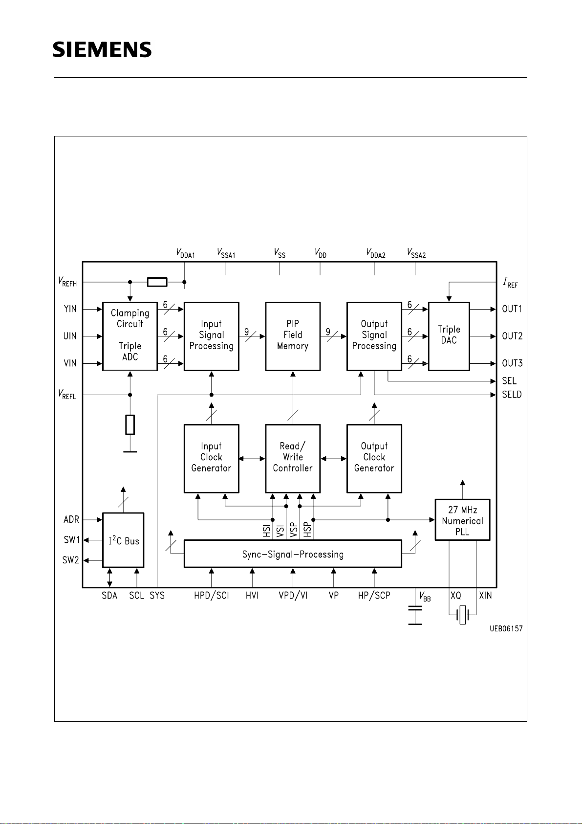
1.4 Functional Block Diagram
SDA 9288X
Figure 2
Semiconductor Group 11 03.96
Page 12

SDA 9288X
2 System Description
2.1 AD Conversion, Inset Synchronization
The inset video signal is fed to the SDA 9288X A141 as analog luminance and
1)
chrominance components
After clamping the video components are AD-converted with an amplitude resolution of
6 bit. The conversion is done using a 13.5 MHz clock for the luminance signal and a
3.375 MHz clock for the chrominance signals.
For the adaption to different application the clamp timing for the analog inputs can be
chosen (CLPS; CLPFIX). Setting this bits to ‘1’ can be useful for non-standard input
signals.
For inset synchronization it is possible to feed either a special 3-level signal via pin HVI
(detection of horizontal and vertical pulses) or separate signals via pins SCI for
horizontal and VI for vertical synchronization. SCI is the horizontal synchron signal of the
inset channel. If the burst gate pulse of the sandcastle is used it must be adapted to
TTL compatible levels by a simple external circuit. Centering of the displayed picture
area is possible by a programmable delay for the horizontal synchronization signal
(HSIDEL).
. The polarity of the chrominance signals is programmable.
The inset horizontal synchronization signals are sampled with 27 MHz. This 27 MHz
clock and the AD converter clocks are derived from the parent horizontal synchronization
pulse (see chapter 2.6) or from the quartz frequency converted by a factor of 4/3.
Delay differences between luminance and chrominance signals at the input of the IC
caused by chroma decoding are compensated by a programmable luminance delay
line (YDEL) of about – 290 ns … 740 ns (at decimation input; see Application
Information).
By analyzing the synchronization pulses the line standard of the inset signal source is
detected and interference noise on the vertical sync signal is removed. For applications
with fixed line standard (only 625 lines or 525 lines) the automatic detection can be
switched off.
The phase of the vertical sync pulse is programmable (VSIDEL; VSPDEL). By this way
a correct detection of the field number is possible, an important condition for frame mode
display.
Note: The adjustment of VSIDEL is influenced by HSIDEL (see chapter 4.3), vertical
synchronization via pin HVI causes an additional internal delay for the vertical
sync pulse of about 16
µ
s.
1)
To improve the signal-to-noise ratio the amplitude of the input signals should be as large as possible.
Semiconductor Group 12 03.96
Page 13

SDA 9288X
2.2 Input Signal Processing
This stage performs the decimation of the inset signal by horizontal and vertical filtering
and sub-sampling. A special antialias filter improves the frequency response of the
luminance channel. It is optimized for the use of the horizontal decimation factor 3:1.
A window signal, derived from the sync pulses and the detected line standard, defines
the part of the active video area used for decimation. For HSIDEL = ‘0’ the decimation
window is opened about 104 clock periods (13.5 MHz) after the horizontal
synchronization pulse. For the 625 lines standard the 36th video line is the first
decimated line, for the 525 lines standard decimation starts in the 26th video line.
The following filters are implemented:
Horizontal Decimation Component Filter
3:1 Luminance 1 + z
–1
3:1 Chrominance 1 + 2 × z–1+z
4:1 Luminance 1 + z–1+z–2+z
4:1 Chrominance 1 + z–1+z–2+z
+z
–2
–2
–3
–3
Vertical Decimation Component Filter
3:1 Luminance 1 + z
–L
3:1 Chrominance 1 + 2 × z–L+z
4:1 Luminance 1 + z–L+z
4:1 Chrominance 1 + z–L+z
jωT
z = e
L = samples per line for luminance respectively chrominance
,T = 1/13.5 MHz for luminance T = 1/3.375 MHz for chrominance
+z
–2L
–2L
–2L
–2L
+z
+z
–3L
–3L
The realized chrominance filtering allows omitting the color decoder delay line for PAL
and SECAM demodulation if the color decoder supplies the same output voltages
independent of the kind of operation. In case of SECAM signals an amplification of the
chrominance signals by a factor of 2 is necessary because just every second line a
signal is present. This chrominance amplification is programmable via pin SYS or
2
I
C Bus (AMSEC).
The horizontal and vertical decimation factors are free programmable (DECHOR,
DECVER). Using different decimations horizontal and vertical 16:9 applications become
realizable:
DECHOR = ‘1’, DECVER = ‘0’: picture size 1/9 for 4:3 inset signals on 16:9 displays
DECHOR = ‘0’, DECVER = ‘1’: picture size 1/16 for 16:9 inset signals on 4:3 displays
Semiconductor Group 13 03.96
Page 14
SDA 9288X
2.3 PIP Field Memory
The on-chip memory stores one decimated field of the inset picture. Its capacity is
169 812 bits. The picture size depends on the horizontal and vertical decimation factors.
Horizontal Decimation PIP PIXELS per Line
Y (B-Y) (R-Y)
3:1 212 53 53
4:1 160 40 40
Vertical Decimation Line Standard PIP Lines
3:1 625 88
3:1 525 76
4:1 625 66
4:1 525 57
In field mode display just every second inset field is written into the memory, in frame
mode display the memory is continuously written. Data are written with the lower inset
clock frequency depending on the horizontal decimation factor (4.5 MHz or 3.375 MHz).
Normally the read frequency is 13.5 MHz and 27 MHz for scan conversion systems.
For progressive scan conversion systems and HDTV displays a line doubling mode is
available (LINEDBL). Every line of the inset picture is read twice.
Memory writing can be stopped by program (FREEZE), a freeze picture display results
(one field).
Having no scan conversion and the same line numbers in inset and parent channel
(625 lines or 525 lines both) frame mode display is possible. The result is a higher
vertical and time resolution because of displaying every incoming field. For this purpose
the standards are internally analysed and activating of frame mode display is blocked
automatically when the described restrictions are not fulfilled.
As in the inset channel a field number detection is carried out for the parent channel.
Depending on the phase between inset and parent signals a correction of the display
raster for the read out data is performed by omitting or inserting lines when the read
address counter outruns the write address counter.
The display position of the inset picture is free programmable (POSHOR, POSVER).
The first possible picture position (without frame) is 54 clock periods (13.5 MHz or
27 MHz) after the horizontal and 4 lines after the vertical synchronization pulses. Starting
at this position the picture can be moved over the whole display area. Even
POP-positions (Picture Outside Picture) at 16:9 applications are possible.
Semiconductor Group 14 03.96
Page 15

SDA 9288X
Having different line standards in inset and parent channels we have a so called mixed
mode display. It causes deformations in the aspect ratio of the inset picture. A special
mixed mode display is available for the picture size 1/9 (MIXDIS):
– Parent channel 625 lines, inset channel 525 lines: The inset picture is shifted down by
6 lines. By performing this shifting the centers of the inset pictures have the same
position for both line standards.
– Parent channel 525 lines, inset channel 625 lines: The inset picture gets a reduced
line number of 76. The first and the last 6 lines are omitted. This way the inset picture
size is the same as for 525 lines inset signals. The display shows the center part of
the original picture.
Synchronization of memory reading with the parent channel is achieved by processing
the parent horizontal and vertical synchronization signals in the same way as described
for the inset channel. The synchronization signals are fed to the IC at pin HP/SCP for
horizontal synchronization and pin VP for vertical synchronization. In the same way as
described for the inset channel the burst gate of the sandcastle signal can be used for
horizontal synchronization. In scan conversion systems also the inputs HPD/SCI and
VPD/VI are available if the input HVI is activated for inset synchronization.
Semiconductor Group 15 03.96
Page 16

SDA 9288X
2.4 Output Signal Processing
At the memory output the chrominance components are demultiplexed and linearly
interpolated to the luminance sample rate.
Different output formats are available: luminance signal Y with inverted or non-inverted
chrominance signals (B-Y), (R-Y) or RGB. For the RGB conversion 3 matrices are
integrated:
Standard B-Y R-Y G-Y B-Y R-Y G-Y
EBU 1 0.558 0.345 0° 90° 237°
NTSC (Japan) 1 0.783 0.31 0° 95° 240°
NTSC (USA) 1 1.013 0.305 0° 104° 252°
2
Matrix selection is done by pin SYS or I
following input voltages (100 % white, 75 % color saturation):
C Bus. The matrices are designed for the
Component Input Voltage (without sync) in % of Full Scale Input Range of ADC
Y75
B-Y 100
R-Y 100
Semiconductor Group 16 03.96
Page 17

2.4.1 Matrix Equations
SDA 9288X
EBU
R
G
B
R
G
B
=
=
101
0 0.78125 1
0.1875– 0.40625– 1
NTSC (Japan)
101
0.0625– 1.09375 1
0.15625– 0.375– 1
BY–
RY–
Y
BY–
RY–
Y
NTSC (USA)
R
G
B
=
101
0.25– 1.375 1
BY–
RY–
0.09375– 0.40625– 1
Y
2.4.2 Frame Insertion
A colored frame is added to the inset picture. 4096 frame colors are programmable,
4 bits for each component Y, (B-Y), (R-Y) (bits FRY, FRU, FRV). The horizontal and
Semiconductor Group 17 03.96
Page 18

SDA 9288X
vertical width of the frame are independently programmable. Width = 0 means display
without frame.
Examples for the Adjustment of Frame Colors
Frame
Color
Blue 0100 0110 1010
Green 0100 1000 1010
White 1100 0000 0000
Red 0100 1000 0111
Yellow 1100 1000 0100
Cyan 1100 0010 1010
Magenta 0100 0110 0100
FRY
D3 … D0 of Subaddress 09
FRU
D3 … D0 of Subaddress 0A
FRV
D7 … D4 of Subaddress 0A
2.4.3 Select Signal
For controlling an external switch (for example an RGB processor) a select signal is
supplied. Pin SEL is active in normal 13.5 MHz reading mode, pin SELD is active using
27 MHz. The phases of these signals are programmable for adaption to different
external output signal processing.
Semiconductor Group 18 03.96
Page 19

SDA 9288X
2.5 DA Conversion
The SDA 9288X A141 includes three 6-bit DA converters. Each converter supplies a
V
current through an external resistor that is connected between
OUT3 respectively. The current is controlled by a digital control circuit. Each command
DACONST or PIPON starts the adjustment cycle.
2.6 PLL
A numerical PLL circuit supplies a clock of about 27 MHz with high stability. The
generated clock is locked to the parent horizontal synchronization pulse. Its frequency
depends linearly on the frequency of the sync signal and the quartz frequency. The
recommended quartz frequencies are listed under ‘Recommended Operation
Conditions’. Using up to three SDA 9288X A141 ICs in one application only a single
quartz is necessary. Four time constants are programmable via I
switched off an external 27 MHz parent line locked clock can be fed to the IC.
and OUT1, OUT2,
SSA
2
C Bus. If the PLL is
The inset clock generation is possible in two ways:
1. Synchron with the parent horizontal synchronization pulse (bit CLISW = ‘0’)
2. Synchron with the quartz frequency (bit CLISW = ‘1’;
= 4/3 × f
cli
). In this mode the
quartz
f
aspect ratio is independent on the parent sync frequency but depends on the used
resonator type. It is only possible to use one of the two modes.
Note: Before setting bit D3 of subaddress 00 (READ27) noise reduction of the
VSP pulse must be switched off (D5 of subaddress 08 = ‘1’).
2.7 I2C Bus
2
2.7.1 I
Three different I
C Bus Addresses
2
C addresses are programmable via pin ADR.
Pin ADR Address (bin.) Address (hex.)
Low level (
V
SS
or V
) 11010110 D6
SSA
Mid level (open) 11011100 DC
High level (
V
DD
or V
) 11011110 DE
DDA
2
2.7.2 I
C Bus Receiver Format
S Address A Subaddress A Data Byte A **** A P
S: start condition A: acknowledge P: stop condition
Only write operation is possible. An automatically address increment function is
implemented.
Semiconductor Group 19 03.96
Page 20

2.7.3 I2C Bus Commands
SDA 9288X
Subaddr.
Hex D7 D6 D5 D4 D3 D2 D1 D0
00 0 SYSACT FREEZE PLLOFF READ27 LINEDBL FRAME PIPON
01 0 SELDEL3 SELDEL2 SELDEL1 SELDEL0 MIXDIS POSHOR9 POSHOR8
02 POSHOR7 POSHOR6 POSHOR5 POSHOR4 POSHOR3 POSHOR2 POSHOR1 POSHOR0
03 POSVER7 POSVER6 POSVER5 POSVER4 POSVER3 POSVER2 POSVER1 POSVER0
04 0 SW21 SW20 SW11 SW10 YDEL2 YDEL1 YDEL0
05 DECVER DECHOR INSHVI CHRINS PMOD1 PMOD0 IMOD1 IMOD0
06 0 CLPS CLPFIX CLISW HSIDEL3 HSIDEL2 HSIDEL1 HSIDEL0
07 AMSEC 0 VSIISQ VSIDEL4 VSIDEL3 VSIDEL2 VSIDEL1 VSIDEL0
08 PARSYND 0 VSPISQ VSPDEL4 VSPDEL3 VSPDEL2 VSPDEL1 VSPDEL0
09 CON3 CON2 CON1 CON0 FRY5 FRY4 FRY3 FRY2
0A FRV5 FRV4 FRV3 FRV2 FRU5 FRU4 FRU3 FRU2
0B 0 0 SELDOWN FRWIDV1 FRWIDV0 FRWIDH2 FRWIDH1 FRWIDH0
0C 0 0 0 MAT2 MAT1 MAT0 CHRPIP OUTFOR
0D DACONST PLLTC1 PLLTC2 0 0 0 0 0
Data Bytes
After switching on the IC the data bytes of all registers are set to ‘0’, the bit PLLOFF is
set to ‘1’.
Semiconductor Group 20 03.96
Page 21

Bit Name Function
Subaddress 00
D0 PIPON 0: PIP insertion OFF
1: PIP insertion ON
D1 FRAME 0: field display
1: frame display (under special restrictions).
Correct adjustment of bits VSIDEL, VSPDEL required
(see chapter 4.3)
D2 LINEDBL 0: each line of the PIP memory is read once
(normal operation)
1: each line of the PIP memory is read twice
(line doubling for progressive scan conversion systems
in parent channel)
SDA 9288X
D3 READ27 0: PIP display with single read frequency (13.5 MHz)
1: PIP display with double read frequency (27 MHz)
(see note page 19).
D4 PLLOFF 0: internal PLL ON
1: internal PLL OFF (external clock generation)
D5 FREEZE 0: live picture
1: freeze picture
D6 SYSACT 0: pin SYS inactive: selection of decimation amplification and
RGB-matrix is done via I
2
C Bus
1: pin SYS active: selection of decimation amplification
and RGB-matrix is done via pin SYS
Subaddress 01
D1 … D0 POSHOR 2 MSBs of POSHOR (see also subaddress 02)
D2 MIXDIS 0: PIP picture height depends just upon inset line standard,
position upon POSHOR
1: modified PIP picture height and position for different inset
and parent line standards (mixed display mode)
D6 … D3 SELDEL Delay of output signal SELECT at pins SEL respectively SELD
(–8…7 periods of read frequency clock, programmable in
2’s complement code). SELDEL = ‘0’: SELECT signal has the
same phase as the PIP picture signal referenced to the
IC output.
Semiconductor Group 21 03.96
Page 22

Bit Name Function
Subaddress 02
D7 … D0 POSHOR Horizontal position of PIP picture (raster: 1 pixel)
Note: The 2 MSBs of POSHOR are located at subaddress 01
Warning: It is not allowed to adjust positions < 2 and > 740.
Note: To avoid horizontal jumping of the picture by changing
POSHOR from ‘00 1111 1111’ to ‘01 0000 0000’ its
necessary to transfer the bits of both subaddresses
during the same field period.
Subaddress 03
SDA 9288X
D7 … D0 POSVER Vertical position of PIP picture (raster: 1 line)
Warning: It is not allowed to adjust positions
> 220 (50 Hz) or > 182 (60 Hz).
Subaddress 04
D2 … D0 YDEL Delay of luminance input signal
000: minimum delay
111: maximum delay; see chapter 4.2
D4 … D3 SW1 Direct control of output pin SW1 (3 levels)
00: low level
01: mid level
10: high level
11: high level
D6 … D5 SW2 Direct control of output pin SW2 (3 levels)
00: low level
01: mid level
10: high level
11: high level
Semiconductor Group 22 03.96
Page 23

SDA 9288X
Bit Name Function
Subaddress 05
D1 … D0 IMOD 00: automatic detection of line standard (inset signal)
01: fixed adjustment 625 lines
10: fixed adjustment 525 lines
11: freeze last line standard
D3 … D2 PMOD 00: automatic detection of line standard (parent signal)
01: fixed adjustment 625 lines
10: fixed adjustment 525 lines
11: freeze last line standard
D4 CHRINS 0: chrominance input signals + (B-Y), + (R-Y)
1: inverted chrominance input signals – (B-Y), – (R-Y)
1)
1)
1)
1)
D5 INSHVI 0: inset synchronization signals via pins HPD/SCI
and VPD/VI
1: inset synchr. signals via pin HVI (3-I. sand-castle signal)
D6 DECHOR 0: horizontal decimation 3 to 1
1: horizontal decimation 4 to 1
D7 DECVER 0: vertical decimation 3 to 1
1: vertical decimation 4 to 1
Subaddress 06
D3 … D0 HSIDEL Delay of horizontal synchronization pulse (inset signal)
Raster: 6 clock periods of 13.5 MHz.
Warning: Adjustment of HSIDEL will influence the adjustment
of VSIDEL (subaddr. 07); see chapter 4.3
D4 CLISW 0: inset clock synchronized with parent clock
1: inset clock synchronized with quartz frequency
Note: Only one of the two modes can be used.
Switching back from ‘1’ to ‘0’ is not possible!
D5 CLPFIX 0: clamp pulses of ADC are dependent on the adjustment
of HSIDEL
1: clamp pulses fixed; no influence of HSIDEL
D6 CLPS 0: three clamp cycles per line (timing see diagram)
1: two clamp cycles per line
1)
Fixed adjustments for IMOD and PMOD result in undefined working conditions when signal standards are
used which are different from the programmed values.
Semiconductor Group 23 03.96
Page 24

SDA 9288X
Bit Name Function
Subaddress 07
D4 … D0 VSIDEL Delay of vertical synchronization pulse (inset signal)
in steps of 2.37 µs.
Warning: Correct adjustment value is influenced by the
adjustment of HSIDEL (subaddr. 06); see chapter 4.3.
D5 VSIISQ Noise reduction of the VSI pulse
(set to ‘0’ under normal conditions)
D7 AMSEC 0: unity amplification of decimation filters (normal mode)
1: amplification by a factor of 2 (SECAM signals without delay
line in the chroma decoder)
Subaddress 08
D4 … D0 VSPDEL Delay of vertical synchronization pulse (parent signal)
in steps of 2.37 µs/1.68 s (50/100 Hz)
D5 VSPISQ Noise reduction of the VSP pulse (should be set to ‘0’ under
normal conditions); in case changing from standard mode to
line or frame conversion modes ‘1’ should be set during the
changement of line frequency
D7 PARSYND 0: parent synchronization signals for double frequency read
via pins HP/SCP and VP
1: parent synchronization signals for double frequency read
via pins HPD/SCI and VPD/VI (INSHVI = ‘1’ required)
Subaddress 09
D3 … D0 FRY Luminance component of frame color (4 MSBs of 6 bit)
D7 … D4 CON Contrast adjustment of PIP picture; steps and adjustment
range depending on the external output resistors.
Proposed value see chapter 3.3
Subaddress 0A
D3 … D0 FRU Chrominance component (B-Y) of frame color
(4 MSBs of 6 bit)
D7 … D4 FRV Chrominance component (R-Y) of frame color
(4 MSBs of 6 bit)
Semiconductor Group 24 03.96
Page 25

Bit Name Function
Subaddress 0B
D2 … D0 FRWIDH Horizontal width of PIP frame (0 … 7 pixels)
D4 … D3 FRWIDV Vertical width of PIP frame (0 … 3 lines)
D5 SELDOWN 0: open source output at pins SEL, SELD
1: TTL output at pins SEL, SELD
Subaddress 0C
D0 OUTFOR 0: format of output signals: Y, (B-Y), (R-Y)
1: format of output signals: R G B
SDA 9288X
D1 CHRPIP 0: chrominance output signals: + (B-Y), + (R-Y)
1: inverted chrominance output signals: – (B-Y), – (R-Y)
D2 MAT0 0: EBU RGB-matrix
1: NTSC RGB-matrix
D3 MAT1 0: preselection of NTSC RGB matrix (USA)
1: preselection of NTSC RBG matrix (Japan)
D4 MAT2 0: matrix selection by bit MAT0
1: automatic matrix selection depending on inset line standard
Subaddress 0D
D0 DACONDE Set to ‘0’
D5 PLLTC2 Time constant of internal PLL:
00: medium damping, low resonance frequency
01: medium damping, high resonance frequency
D6 PLLTC1 10: high damping, low resonance frequency
11: high damping, high resonance frequency
Note: After power ON PLLTC must remain at 00
until the system is locked.
D7 DACONST Changing from ‘0’ to ‘1’ starts automatic adjustment of
OUT1 … 3 output current (switching PIPON gives the
same result).
Semiconductor Group 25 03.96
Page 26

3 Electrical Characteristics
3.1 Absolute Maximum Ratings
Parameter Symbol Limit Values Unit Remark
min. max.
SDA 9288X
Ambient temperature
Storage temperature
Junction temperature
Soldering temperature
Input voltage
Output voltage
T
T
T
T
V
V
V
A
stg
j
SOLD
I
I
Q
070°C
– 55 125 °C
125 °C
260 °C Duration < 10 s
– 0.5 V VDD+
0.5 V
1 Analog inputs
(YIN, UIN, VIN,
– 1 7 V All other pins
– 0.5 V VDD+
0.5 V
1 Pins OUT1, OUT2,
OUT3, XQ, SW1,
I
REF
SW2
Supply voltages
Supply voltage differentials
Total power dissipation
V
V
V
P
Q
DD
DD D
tot
– 1 7 V All other pins
–1 7 V
– 0.25 0.25 V
900 mW
Latch-up protection – 100 100 mA Except pins OUT1,
OUT2, OUT3,
I
REF
XQ, XQ, YIN, UIN,
VIN
)
,
Note: All voltages listed are referenced to ground (0 V,
V
) except where noted.
SS
Stresses above those listed here may cause permanent damage to the device.
Exposure to absolute maximum rating conditions for extended periods may affect
device reliability.
Semiconductor Group 26 03.96
Page 27

3.2 Operational Range
Parameter Symbol Limit Values Unit Remark
min. typ. max.
SDA 9288X
Supply voltages
Ambient temperature
V
T
DDxx
A
4.75 5 5.5 V
02570°C
All TTL Inputs
Low-level input
V
IL
– 1 0.8 V
voltage
High-level input
V
IH
2.0 6 V
voltage
All Three Level Inputs (3-L) (see figure)
High-level input
V
IH
3.5 6 V
voltage
Low-level input
V
IL
– 1 0.8 V
voltage
Medium-level voltage
V
IM
Open input,
see chapter 3.3
All 3-L Outputs (see figure)
High-level output
I
OH
– 500 0 µA
current
Low-level output
I
OL
0 1.6 mA
current
Inset Horizontal Sync TTL and 3-L Inputs: HPD/SCI, HVI
1)
Horizontal frequency 14.53 16.72 kHz
Signal rise time 100 ns Noisefree L/M-to-H
transition
Signal high time 100 ns
Signal medium
900 ns
or low time
1)
All values are referred to the corresponding min (VIH), max (VIM) and max (VIL)
Semiconductor Group 27 03.96
Page 28

3.2 Operational Range (cont’d)
Parameter Symbol Limit Values Unit Remark
min. typ. max.
SDA 9288X
Inset Vertical Sync TTL and 3-L Inputs: VPD/VI, HVI
Signal medium
17 µs Necessary for vertical
or high time
1)
sync detection
Signal low time 200 ns
Parent Horizontal Sync TTL Inputs: HP/SCP, HPD/SCI
Sync frequency
14.53 16.72 kHz Quartz frequency
in single frequency
display mode
15 17.19 kHz Quartz frequency
2)
20.480 MHz
21.090 MHz
Sync frequency
in double frequency
display mode
29.06 33.44 kHz Quartz frequency
20.480 MHz
30 34.375 kHz Quartz frequency
21.090 MHz
Signal rise time 100 ns Noisefree transition
Signal high time 100 ns
Signal low time 900 ns
Parent Vertical Sync TTL Input VDP/VI
2)
Signal HIGH time 200 ns
Signal LOW time 200 ns
1)
All values are referred to the corresponding min (VIH), max (VIM) and max (VIL)
2)
All values are referred to the corresponding min (VIH) and max (VIL)
Semiconductor Group 28 03.96
Page 29

3.2 Operational Range (cont’d)
Parameter Symbol Limit Values Unit Remark
min. typ. max.
SDA 9288X
Quartz/Ceramic Resonator
Recommended
2)
20.25 20.48 21.3 MHz 21.09 MHz for MUSE
frequency
Series resistance 10 Ω
20 Ω
30 Ω
40 Ω
C
, C2≤ 33 pF
1
C
, C2≤ 22 pF
1
C
, C2≤ 15 pF
1
C
, C2≤ 10 pF
1
(total series
capacitance)
Optional TTL Clock Input: XIN
1)
Clock input cycle time 35 40 ns External line locked;
Clock input rise time 5 ns
Clock input fall time 5 ns
27 MHz clock
2
(I
C: internal PLL
OFF)
Clock input low time 10 ns
Clock input high time 10 ns
Fast I
2
C Bus
SCL clock frequency f
Inactive time before
1) 3)
t
SCL
BUF
0 400 kHz
1.3 µs
start of transmission
Setup time
t
SU; STA
0.6 µs
start condition
Hold time start
t
HD; STA
0.6 µs
condition
SCL low time
1)
All values are referred to min (VIH) and max (VIL).
2)
There is no internal protection for the crystal driver against oscillation at harmonic frequencies.
3)
This specification of the bus lines does not have to be identical with the I/O stages specification because of
optional series resistors between bus lines and I/O pins.
t
LOW
1.3 µs
Semiconductor Group 29 03.96
Page 30

3.2 Operational Range (cont’d)
Parameter Symbol Limit Values Unit Remark
min. typ. max.
SDA 9288X
SCL high time t
Setup time data
Hold time data
SDA/SCL rise/fall
HIGH
t
SU; DAT
t
HD;DAT
t
, t
R
F
times
Setup time stop
t
SU; STO
condition
Capacitive load/bus
C
b
line
2
C Bus Inputs/Output: SDA, SCL
I
High-level input
V
IH
voltage
Low-level input
V
IL
voltage
Spike duration at
inputs
0.6 µs
100 ns
0 0.9 µs
20 + $ 300 ns $ = 0.1Cb/pF
0.6 µs
400 pF
3 V
+ 0.5
DD
V Also for SDA/SCL
input stages
– 0.5 1.5 V
0050ns
Low-level output
I
OL
current
Analog to Digital Converters (6 bit)
Input coupling
10 100 nF Necessary for proper
capacitors
Y, U, V source
resistance
Reference voltage
V
REFL
0.5 1.0 1.5 V Min and max values
low
Reference voltage
V
REFH
1.5 2.0 2.5 V
high
Reference voltage
difference
V
V
REFH
REFL
–
0.5 1.0 2 V
6mA
clamping
1kΩ
only with optional
external resistors,
see also chapter 3.3.
Semiconductor Group 30 03.96
Page 31

3.2 Operational Range (cont’d)
Parameter Symbol Limit Values Unit Remark
min. typ. max.
Digital-to-Analog Converters (6 bit)
SDA 9288X
Full range output
V
OFR
1 2 V Peak to peak
voltage
Reference resistance
R
REF1
4.2 5.1 6.3 kΩ Bits CON = ‘0000’;
no contrast
adjustment used
R
REF2
6.0 6.8 7.5 kΩ Contrast adjustment
2
via I
C Bus
Note: In the operational range the functions given in the circuit description are fulfilled.
Semiconductor Group 31 03.96
Page 32

3.3 Characteristics
Parameter Symbol Limit Values Unit Remark
min. max.
SDA 9288X
Average total supply current
Average digital supply current I
Average analog supply current
Average analog supply current
All Digital Inputs (TTL, I
2
C)
Input capacitance
I
DDtot
DD
I
DDA1
I
DDA2
C
160 mA I
120 mA
40 mA
= IDD+ I
DDtot
DDA1
Note: The maxima do
not necessarily
coincide.
20 mA
I
7 pF Not tested
Input leakage current – 10 10 µA Including leakage
current of SDA output
stage
All Three Level Inputs (3-L) (see figure)
Input capacitance
Medium-level open input
C
V
IM
I
7 pF Not tested
2.1 2.5 V |IIN| ≤ 1 µA, VDD = 5 V
voltage
+ I
DDA2
Differential input resistance
R
IN
814kΩNot tested
SEL, SELD
High-level output voltage V
High-level output voltage
Low-level output voltage
V
V
OH
OH
OL
2.4 V V
1.5 V V
0.4 V IOL= 1.6 mA, only valid
DD
DD
V IOH= – 200 µA
V IOH= – 4.5 mA
if bit SELDOWN = ‘1’
Leakage current – 10 A
V
=0V…V
O
Output capacitance 7 pF Not tested
All 3-L Outputs
High-level output voltage V
High-level output voltage
Low-level output voltage
V
V
OH
OH
OL
4VI
= – 100 µA
OH
3.9 V IOH = – 500 µA
0.4 V IOL = max
DD
Semiconductor Group 32 03.96
Page 33

3.3 Characteristics (cont’d)
Parameter Symbol Limit Values Unit Remark
min. max.
SDA 9288X
Medium-level output leakage
I
OM
–1 1 µA Tristate
current
Output capacitance 7 pF Not tested
2
I
C Inputs: SDA/SCL
Schmitt trigger hysteresis
2
I
C Input/Output: SDA (referenced to SCL; open drain output)
Low-level output voltage
Low-level output voltage
Output fall time from
min (
V
) to max (VIL)
IH
V
V
V
t
hys
OL
OL
OF
0.2 V Not tested
0.4 V IOL=3mA
0.6 V IOL= max
20 +
250 ns 10 pF ≤
C
0.1 ×
C
/pF
b
Analog-to-Digital Converters (6 bit)
Y, U, V input leakage current – 100 100 nA
≤ 400 pF
b
Y, U, V input capitance 7 pF Not tested
Input clamping error – 1 1 LSB Settled state
Input clamping current |I
Reference voltage difference
|15
CLP
V
–
REFH
V
REFL
40
70
50
90
150
µA
µA
µA
Deviation < 1 LSB
Deviation 1…2LSB
Deviation > 2 LSB
0.98 1.02 V V
(
DDA
V
REFH
= nom,
– V
REFL
≅V
DDA1
Digital-to-Analog Converters (6 bit): Current Source Outputs OUT1, OUT2, OUT3
D.C. differential nonlinearity DNLE – 0.5 0.5 LSB R
Full range output current
I
O
– 1.42– 1.73mA V
= 5.1 kΩ
REF
= max, TA = nom,
DDA
R
= 5.1 kΩ,
REF
R
= 680 Ω,
L
after adjustment
/5)
1)
Semiconductor Group 33 03.96
Page 34

3.3 Characteristics (cont’d)
Parameter Symbol Limit Values Unit Remark
min. max.
SDA 9288X
Output voltage
(
V
1.6 × V
ON
DDA
× RL/R
REF
)
V
O
0.96 1.18 V V
Tracking – 3 3 %
Contrast increase 30 %
Supply voltage dependence of
DAC output current
Temperature dependence of
DAC output current
= max, TA = nom,
DDA
R
= 680 Ω,
L
R
= 5.1 kΩ,
REF
after adjustment
V
= max, TA = nom,
DDA
R
= 5.1 kΩ,
REF
R
= 680 Ω
L
V
= nom, TA = nom,
DDA
R
= 680 Ω,
L
R
= 6.8 kΩ,
REF
contrast bits change
from ‘0000’ to ‘1111’
for typical values
see chapter 4
For typical values
see chapter 4
For typical values
see chapter 4
Dependence of DAC output
current on external reference
For typical values
see chapter 4
resistor
1)I2
C: Contrast bits set to zero unless otherwise noted.
Note: The listed characteristics are ensured over the operating range of the integrated
circuit unless restricted to nominal operating conditions (all voltages refer to
V
SS
).
The listed characteristics are ensured over the operating range of the integrated
circuit. Typical characteristics specify mean values expected over the production
spread. If not otherwise specified, typical characteristics apply at
T
= 25°C and
A
the given supply voltage.
Semiconductor Group 34 03.96
Page 35

SDA 9288X
4 Diagrams
4.1 Output Current of DA Converters
V
Nominal values:
= 5 V; V
DDA
Measurements after adjustment via bit d7 of I
Note: The output currents are controlled in digital way, so inaccuracy of 1 LSB (ca. 2 %)
is always possible.
= 5.1 kΩ; T = 25 °C
REF
2
C Bus address 0D for each step
Output current = f (V
) Output current = f (TA)
DDA
Semiconductor Group 35 03.96
Page 36

SDA 9288X
Output current = f (R
) Current = f (CON 0 … 3)
REF
Semiconductor Group 36 03.96
Page 37

4.2 Application Information
4.2.1 Reference Voltage Generation for ADC
SDA 9288X
Figure 3
Signal Input Range 1 Vpp at Y, U, V
Figure 4
Signal Input Range 2 Vpp at Y, U, V
Semiconductor Group 37 03.96
Page 38

SDA 9288X
Figure 5
Signal Input Range 0.5 Vpp at Y, U, V
Semiconductor Group 38 03.96
Page 39

4.2.2 Adjustment of YDEL
SDA 9288X
Figure 6
Semiconductor Group 39 03.96
Page 40

4.2.3 Three Level Interface (3-L)
SDA 9288X
Figure 7
High level (H): upper transistor ON, lower transistor OFF
Medium level (M): both transistors OFF (interface voltage determined by input stage)
Low level (L): upper transistor OFF, lower transistor ON
Semiconductor Group 40 03.96
Page 41

4.2.4 Application Board Layout Proposal
SDA 9288X
Figure 8
(top view)
Figure 9
(bottom view)
Semiconductor Group 41 03.96
Page 42

4.2.5 Application Circuit (R, G, B-mode)
SDA 9288X
Figure 10
Semiconductor Group 42 03.96
Page 43

4.3 Waveforms
4.3.1 Timing of ADC Clamping
SDA 9288X
Figure 11
The values are valid if HSIDEL = ‘0’. To get the maximum values 444 ns for each step
of HSIDEL adjustment must be added (CLPFIX = ‘0’). With CLPFIX = ‘1’ there is no
influence of the HSIDEL adjustment to the clamp timing.
Semiconductor Group 43 03.96
Page 44

SDA 9288X
4.3.2 Phase Relation of Sync Pulses at Frame Mode
If the phase relation is not correct at the H and V sync inputs, an adjustment via bits
VSIDEL and VSPDEL is possible.
Figure 12
Signal Flow of the Horizontal Synchronization (insert part)
Figure 13
Allowed Phase Relation of the
Horizontal/Vertical Sync Pulses (insert channel) if VSIDEL(0:4) = ‘0000’
Semiconductor Group 44 03.96
Page 45

SDA 9288X
Figure 14
Allowed Phase Relation of the
Horizontal/Vertical Sync Pulses (parent channel)if VSIDEL(0:4) = ‘0000’
Semiconductor Group 45 03.96
Page 46

5 Package Outlines
P-DSO-32-2
(Plastic Dual Small Outline Package)
SDA 9288X
Sorts of Packing
Package outlines for tubes, trays etc. are contained in our
Data Book “Package Information”
SMD = Surface Mounted Device
Semiconductor Group 46 03.96
Dimensions in mm
GPS05697
 Loading...