

Page 1

USER’S MANUAL
M2
SDA 6000
Teletext Decoder
with Embedded
16-bit Controller
Edition March 1, 2001
6251-557-1
Page 2

SDA 6000
Revision History: Current Version: 2000-06-15
Previous Version: 08.99
Page Subjects (major changes since last revision)
Complete Update of Controller & Peripheral Spec --> Detailed Version
ASC: Autobaud Detection Feature included
IC: New Description
GPT: New Description
IIC changed to I
2
C
For questions on technology, delivery and prices please contact the Micronas Offices in Germany
or the Micronas GmbH Companies and Representatives worldwide:
see our webpage at http://www.micronas.com
Page 3

Contents
Overview
Page 4

SDA 6000 PRELIMINARY DATA SHEET
Version 2.1
1Overview . . . . . . . . . . . . . . . . . . . . . . . . . . . . . . . . . . . . . . . . . . . . . . . . 1 - 3
1.1 Features . . . . . . . . . . . . . . . . . . . . . . . . . . . . . . . . . . . . . . . . . . . . . . . . . 1 - 7
1.2 Logic Symbol . . . . . . . . . . . . . . . . . . . . . . . . . . . . . . . . . . . . . . . . . . . . . 1 - 9
2 Pin Descriptions . . . . . . . . . . . . . . . . . . . . . . . . . . . . . . . . . . . . . . . . . 2 - 3
2.1 Pin Diagram (top view) . . . . . . . . . . . . . . . . . . . . . . . . . . . . . . . . . . . . . 2 - 3
2.2 Pin Definitions and Functions . . . . . . . . . . . . . . . . . . . . . . . . . . . . . . . . 2 - 4
3 Architectural Overview . . . . . . . . . . . . . . . . . . . . . . . . . . . . . . . . . . . . 3 - 3
4 C16X Microcontroller . . . . . . . . . . . . . . . . . . . . . . . . . . . . . . . . . . . . . . 4 - 3
4.1 Overview . . . . . . . . . . . . . . . . . . . . . . . . . . . . . . . . . . . . . . . . . . . . . . . . 4 - 3
4.2 Memory Organization . . . . . . . . . . . . . . . . . . . . . . . . . . . . . . . . . . . . . . 4 - 5
4.3 On-Chip Microcontroller RAM and SFR Area . . . . . . . . . . . . . . . . . . . . 4 - 7
4.3.1 System Stack . . . . . . . . . . . . . . . . . . . . . . . . . . . . . . . . . . . . . . . . . . 4 - 9
4.3.2 General Purpose Registers . . . . . . . . . . . . . . . . . . . . . . . . . . . . . . . . 4 - 9
4.3.3 PEC Source and Destination Pointers . . . . . . . . . . . . . . . . . . . . . . . 4 - 10
4.3.4 Special Function Registers . . . . . . . . . . . . . . . . . . . . . . . . . . . . . . . 4 - 11
4.4 External Memory . . . . . . . . . . . . . . . . . . . . . . . . . . . . . . . . . . . . . . . . . 4 - 12
4.4.1 SDRAM . . . . . . . . . . . . . . . . . . . . . . . . . . . . . . . . . . . . . . . . . . . . . . 4 - 13
4.4.2 External Static Memory Devices . . . . . . . . . . . . . . . . . . . . . . . . . . . 4 - 13
4.5 External Bus Interface (EBI). . . . . . . . . . . . . . . . . . . . . . . . . . . . . . . . . 4 - 13
4.5.1 Memory Mapping . . . . . . . . . . . . . . . . . . . . . . . . . . . . . . . . . . . . . . . 4 - 16
4.5.2 Register Description . . . . . . . . . . . . . . . . . . . . . . . . . . . . . . . . . . . . 4 - 19
4.5.3 Crossing Memory Boundaries . . . . . . . . . . . . . . . . . . . . . . . . . . . . 4 - 23
4.6 Central Processing Unit . . . . . . . . . . . . . . . . . . . . . . . . . . . . . . . . . . . . 4 - 24
4.6.1 Instruction Pipelining . . . . . . . . . . . . . . . . . . . . . . . . . . . . . . . . . . . . 4 - 26
4.6.2 Bit-Handling and Bit-Protection . . . . . . . . . . . . . . . . . . . . . . . . . . . 4 - 32
4.6.3 Instruction State Times . . . . . . . . . . . . . . . . . . . . . . . . . . . . . . . . . 4 - 33
4.6.4 CPU Special Function Registers . . . . . . . . . . . . . . . . . . . . . . . . . . . 4 - 34
5 Interrupt and Trap Functions . . . . . . . . . . . . . . . . . . . . . . . . . . . . . . . 5 - 3
5.1 Interrupt System Structure . . . . . . . . . . . . . . . . . . . . . . . . . . . . . . . . . . . 5 - 3
5.1.1 Interrupt Allocation Table . . . . . . . . . . . . . . . . . . . . . . . . . . . . . . . . . . 5 - 4
5.1.2 Hardware Traps . . . . . . . . . . . . . . . . . . . . . . . . . . . . . . . . . . . . . . . . . 5 - 6
5.2 Operation of the PEC Channels . . . . . . . . . . . . . . . . . . . . . . . . . . . . 5 - 13
5.2.1 Prioritization of Interrupt and PEC Service Requests . . . . . . . . . . . 5 - 20
5.2.2 Saving the Status during Interrupt Service . . . . . . . . . . . . . . . . . . . 5 - 22
5.2.3 Interrupt Response Times . . . . . . . . . . . . . . . . . . . . . . . . . . . . . . . 5 - 23
5.2.4 PEC Response Times . . . . . . . . . . . . . . . . . . . . . . . . . . . . . . . . . . 5 - 25
5.2.5 Fast Interrupts . . . . . . . . . . . . . . . . . . . . . . . . . . . . . . . . . . . . . . . . 5 - 27
5.3 Trap Functions . . . . . . . . . . . . . . . . . . . . . . . . . . . . . . . . . . . . . . . . . . 5 - 28
5.3.1 External Interrupt Source Control . . . . . . . . . . . . . . . . . . . . . . . . . . 5 - 33
6 System Control & Configuration . . . . . . . . . . . . . . . . . . . . . . . . . . . . 6 - 3
A-3 Micronas
Page 5

SDA 6000 PRELIMINARY DATA SHEET
Version 2.1
6.1 System Reset . . . . . . . . . . . . . . . . . . . . . . . . . . . . . . . . . . . . . . . . . . . . 6 - 3
6.1.1 Behavior of I/Os during Reset . . . . . . . . . . . . . . . . . . . . . . . . . . . . . . 6 - 5
6.1.2 Reset Values for the Controller Core Registers . . . . . . . . . . . . . . . . . 6 - 5
6.1.3 The Internal RAM after Reset . . . . . . . . . . . . . . . . . . . . . . . . . . . . . . 6 - 5
6.2 System Start-up Configuration . . . . . . . . . . . . . . . . . . . . . . . . . . . . . . . . 6 - 5
6.3 Register Write Protection . . . . . . . . . . . . . . . . . . . . . . . . . . . . . . . . . . . . 6 - 8
6.4 Power Reduction Modes . . . . . . . . . . . . . . . . . . . . . . . . . . . . . . . . . . . 6 - 12
6.5 Dedicated Pins . . . . . . . . . . . . . . . . . . . . . . . . . . . . . . . . . . . . . . . . . . . 6 - 15
6.6 XBUS Configuration . . . . . . . . . . . . . . . . . . . . . . . . . . . . . . . . . . . . . . . 6 - 17
6.7 Watchdog Timer . . . . . . . . . . . . . . . . . . . . . . . . . . . . . . . . . . . . . . . . . 6 - 17
6.8 Bootstrap Loader . . . . . . . . . . . . . . . . . . . . . . . . . . . . . . . . . . . . . . . . . 6 - 21
6.9 Identification Registers . . . . . . . . . . . . . . . . . . . . . . . . . . . . . . . . . . . . 6 - 23
6.9.1 System Identification . . . . . . . . . . . . . . . . . . . . . . . . . . . . . . . . . . . . 6 - 23
6.9.2 CPU Identification . . . . . . . . . . . . . . . . . . . . . . . . . . . . . . . . . . . . . . 6 - 26
6.10 Parallel Ports . . . . . . . . . . . . . . . . . . . . . . . . . . . . . . . . . . . . . . . . . . . . 6 - 27
7 Peripherals . . . . . . . . . . . . . . . . . . . . . . . . . . . . . . . . . . . . . . . . . . . . . . 7 - 3
7.1 General Purpose Timer Unit . . . . . . . . . . . . . . . . . . . . . . . . . . . . . . . . . 7 - 3
7.1.1 Functional Description of Timer Block 1 . . . . . . . . . . . . . . . . . . . . . . 7 - 3
7.1.1.1 Timer Concatenation . . . . . . . . . . . . . . . . . . . . . . . . . . . . . . . . . . 7 - 14
7.1.2 Functional Description of Timer Block 2 . . . . . . . . . . . . . . . . . . . . . 7 - 19
7.1.2.1 Core Timer T6 . . . . . . . . . . . . . . . . . . . . . . . . . . . . . . . . . . . . . . . 7 - 20
7.1.2.2 Auxiliary Timer T5 . . . . . . . . . . . . . . . . . . . . . . . . . . . . . . . . . . . . 7 - 21
7.1.2.3 Timer Concatenation . . . . . . . . . . . . . . . . . . . . . . . . . . . . . . . . . . 7 - 22
7.1.3 GPT Registers . . . . . . . . . . . . . . . . . . . . . . . . . . . . . . . . . . . . . . . . . 7 - 26
7.1.4 Interrupts . . . . . . . . . . . . . . . . . . . . . . . . . . . . . . . . . . . . . . . . . . . . . 7 - 37
7.2 Real-time Clock . . . . . . . . . . . . . . . . . . . . . . . . . . . . . . . . . . . . . . . . . . 7 - 39
7.2.1 General Description . . . . . . . . . . . . . . . . . . . . . . . . . . . . . . . . . . . . . 7 - 39
7.2.2 Register Description . . . . . . . . . . . . . . . . . . . . . . . . . . . . . . . . . . . . 7 - 41
7.3 Asynchronous/Synchronous Serial Interface . . . . . . . . . . . . . . . . . . . . 7 - 46
7.3.1 Asynchronous Operation . . . . . . . . . . . . . . . . . . . . . . . . . . . . . . . . . 7 - 49
7.3.1.1 Asynchronous Data Frames . . . . . . . . . . . . . . . . . . . . . . . . . . . . 7 - 51
7.3.1.2 Asynchronous Transmission . . . . . . . . . . . . . . . . . . . . . . . . . . . . 7 - 53
7.3.1.3 Asynchronous Reception . . . . . . . . . . . . . . . . . . . . . . . . . . . . . . . 7 - 54
7.3.2 Synchronous Operation . . . . . . . . . . . . . . . . . . . . . . . . . . . . . . . . . . 7 - 56
7.3.2.1 Synchronous Transmission . . . . . . . . . . . . . . . . . . . . . . . . . . . . . 7 - 57
7.3.2.2 Synchronous Reception . . . . . . . . . . . . . . . . . . . . . . . . . . . . . . . . 7 - 58
7.3.2.3 Synchronous Timing . . . . . . . . . . . . . . . . . . . . . . . . . . . . . . . . . . 7 - 58
7.3.3 Baud Rate Generation . . . . . . . . . . . . . . . . . . . . . . . . . . . . . . . . . . . 7 - 59
7.3.3.1 Baud Rates in Asynchronous Mode . . . . . . . . . . . . . . . . . . . . . . 7 - 60
7.3.3.2 Baud Rates in Synchronous Mode . . . . . . . . . . . . . . . . . . . . . . . 7 - 63
7.3.4 Autobaud Detection . . . . . . . . . . . . . . . . . . . . . . . . . . . . . . . . . . . . . 7 - 63
7.3.4.1 Serial Frames for Autobaud Detection . . . . . . . . . . . . . . . . . . . . . 7 - 64
A-4 Micronas
Page 6

SDA 6000 PRELIMINARY DATA SHEET
Version 2.1
7.3.4.2 Baud Rate Selection and Calculation . . . . . . . . . . . . . . . . . . . . . 7 - 67
7.3.4.3 Overwriting Registers on Successful Autobaud Detection . . . . . 7 - 69
7.3.5 ASC Hardware Error Detection Capabilities . . . . . . . . . . . . . . . . . . 7 - 70
7.3.6 Interrupts . . . . . . . . . . . . . . . . . . . . . . . . . . . . . . . . . . . . . . . . . . . . . 7 - 71
7.3.7 Register Description . . . . . . . . . . . . . . . . . . . . . . . . . . . . . . . . . . . . 7 - 72
7.4 High Speed Synchronous Serial Interface . . . . . . . . . . . . . . . . . . . . . . 7 - 82
7.4.1 Full-Duplex Operation . . . . . . . . . . . . . . . . . . . . . . . . . . . . . . . . . . . 7 - 86
7.4.2 Half Duplex Operation . . . . . . . . . . . . . . . . . . . . . . . . . . . . . . . . . . . 7 - 89
7.4.3 Continuous Transfers . . . . . . . . . . . . . . . . . . . . . . . . . . . . . . . . . . . 7 - 90
7.4.4 Port Control . . . . . . . . . . . . . . . . . . . . . . . . . . . . . . . . . . . . . . . . . . . 7 - 91
7.4.5 Baud Rate Generation . . . . . . . . . . . . . . . . . . . . . . . . . . . . . . . . . . . 7 - 91
7.4.6 Error Detection Mechanisms . . . . . . . . . . . . . . . . . . . . . . . . . . . . . . 7 - 92
7.4.7 Register Description . . . . . . . . . . . . . . . . . . . . . . . . . . . . . . . . . . . . 7 - 95
7.5 I2C-Bus Interface . . . . . . . . . . . . . . . . . . . . . . . . . . . . . . . . . . . . . . . . . 7 - 99
7.5.1 Operational Overview . . . . . . . . . . . . . . . . . . . . . . . . . . . . . . . . . . 7 - 100
2
7.5.2 The Physical I
7.5.3 Functional Overview . . . . . . . . . . . . . . . . . . . . . . . . . . . . . . . . . . . 7 - 103
7.5.4 Registers . . . . . . . . . . . . . . . . . . . . . . . . . . . . . . . . . . . . . . . . . . . . 7 - 105
7.6 Analog Digital Converter . . . . . . . . . . . . . . . . . . . . . . . . . . . . . . . . . . 7 - 118
7.6.1 Power Down and Wake Up . . . . . . . . . . . . . . . . . . . . . . . . . . . . . . 7 - 119
7.6.2 Register Description . . . . . . . . . . . . . . . . . . . . . . . . . . . . . . . . . . . 7 - 119
C-Bus Interface . . . . . . . . . . . . . . . . . . . . . . . . . . . 7 - 100
8 Clock System . . . . . . . . . . . . . . . . . . . . . . . . . . . . . . . . . . . . . . . . . . . . 8 - 3
8.1 General Function . . . . . . . . . . . . . . . . . . . . . . . . . . . . . . . . . . . . . . . . . . 8 - 3
8.2 Register Description . . . . . . . . . . . . . . . . . . . . . . . . . . . . . . . . . . . . . . . 8 - 4
9 Sync System . . . . . . . . . . . . . . . . . . . . . . . . . . . . . . . . . . . . . . . . . . . . 9 - 3
9.1 General Description . . . . . . . . . . . . . . . . . . . . . . . . . . . . . . . . . . . . . . . . 9 - 3
9.1.1 Screen Resolution . . . . . . . . . . . . . . . . . . . . . . . . . . . . . . . . . . . . . . . 9 - 3
9.1.2 Sync Interrupts . . . . . . . . . . . . . . . . . . . . . . . . . . . . . . . . . . . . . . . . . . 9 - 5
9.2 Register Description . . . . . . . . . . . . . . . . . . . . . . . . . . . . . . . . . . . . . . . 9 - 6
10 Display Generator . . . . . . . . . . . . . . . . . . . . . . . . . . . . . . . . . . . . . . . 10 - 3
10.1 General Description . . . . . . . . . . . . . . . . . . . . . . . . . . . . . . . . . . . . . . . 10 - 3
10.2 Screen Alignments . . . . . . . . . . . . . . . . . . . . . . . . . . . . . . . . . . . . . . . . 10 - 3
10.3 Layer Concept . . . . . . . . . . . . . . . . . . . . . . . . . . . . . . . . . . . . . . . . . . . 10 - 5
10.3.1 Overlapped Layers . . . . . . . . . . . . . . . . . . . . . . . . . . . . . . . . . . . . . 10 - 6
10.3.2 Embedded Layers . . . . . . . . . . . . . . . . . . . . . . . . . . . . . . . . . . . . . . 10 - 8
10.3.3 Transparency in Screen Background Area . . . . . . . . . . . . . . . . . . . 10 - 9
10.4 Input and Output Formats . . . . . . . . . . . . . . . . . . . . . . . . . . . . . . . . . 10 - 11
10.4.1 Input Formats . . . . . . . . . . . . . . . . . . . . . . . . . . . . . . . . . . . . . . . . . 10 - 12
10.4.2 Output Formats . . . . . . . . . . . . . . . . . . . . . . . . . . . . . . . . . . . . . . . 10 - 13
10.5 Initialization of Memory Transfers . . . . . . . . . . . . . . . . . . . . . . . . . . . 10 - 17
10.5.1 Transfer Modes . . . . . . . . . . . . . . . . . . . . . . . . . . . . . . . . . . . . . . . 10 - 17
A-5 Micronas
Page 7

SDA 6000 PRELIMINARY DATA SHEET
Version 2.1
10.5.2 Transfer Areas . . . . . . . . . . . . . . . . . . . . . . . . . . . . . . . . . . . . . . . . 10 - 20
10.5.3 Italic Mode . . . . . . . . . . . . . . . . . . . . . . . . . . . . . . . . . . . . . . . . . . . 10 - 25
10.6 Register Description . . . . . . . . . . . . . . . . . . . . . . . . . . . . . . . . . . . . . 10 - 27
10.6.1 Special Function Registers . . . . . . . . . . . . . . . . . . . . . . . . . . . . . . 10 - 27
10.7 Description of Graphic Accelerator Instructions . . . . . . . . . . . . . . . . . 10 - 30
10.7.1 Screen Attributes (SAR) . . . . . . . . . . . . . . . . . . . . . . . . . . . . . . . . 10 - 32
10.7.2 Startaddress of Layer 1 (FBR) . . . . . . . . . . . . . . . . . . . . . . . . . . . . 10 - 35
10.7.3 Size of Layer 1 (FSR) . . . . . . . . . . . . . . . . . . . . . . . . . . . . . . . . . . 10 - 35
10.7.4 Startaddress of Layer 2 (DBR) . . . . . . . . . . . . . . . . . . . . . . . . . . . 10 - 36
10.7.5 Size of Layer 2 (DSR) . . . . . . . . . . . . . . . . . . . . . . . . . . . . . . . . . . 10 - 36
10.7.6 Display Coordinates of Layer 2 (DCR) . . . . . . . . . . . . . . . . . . . . . 10 - 37
10.7.7 Contents of CLUT (CLR) . . . . . . . . . . . . . . . . . . . . . . . . . . . . . . . . 10 - 38
10.7.8 Clipping Coordinates (CUR and CBR) . . . . . . . . . . . . . . . . . . . . . . 10 - 38
10.7.9 Source Descriptor for Data Transfer (SDR) . . . . . . . . . . . . . . . . . . 10 - 40
10.7.10 Source Size of Transferred Memory Area (TSR) . . . . . . . . . . . . . . 10 - 41
10.7.11 Destination Size of Transferred Memory Area (TDR) . . . . . . . . . . 10 - 42
10.7.12 Offset of Transferred Memory Area (TOR) . . . . . . . . . . . . . . . . . . 10 - 43
10.7.13 Attributes of Transfer (TAR) . . . . . . . . . . . . . . . . . . . . . . . . . . . . . . 10 - 44
11 D/A Converter . . . . . . . . . . . . . . . . . . . . . . . . . . . . . . . . . . . . . . . . . . . 11 - 3
11.1 Register Description . . . . . . . . . . . . . . . . . . . . . . . . . . . . . . . . . . . . . . 11 - 3
12 Slicer and Acquisition . . . . . . . . . . . . . . . . . . . . . . . . . . . . . . . . . . . . 12 - 3
12.1 General Function . . . . . . . . . . . . . . . . . . . . . . . . . . . . . . . . . . . . . . . . . 12 - 3
12.2 Slicer Architecture . . . . . . . . . . . . . . . . . . . . . . . . . . . . . . . . . . . . . . . . 12 - 3
12.2.1 Distortion Processing . . . . . . . . . . . . . . . . . . . . . . . . . . . . . . . . . . . . 12 - 5
12.2.2 Data Separation . . . . . . . . . . . . . . . . . . . . . . . . . . . . . . . . . . . . . . . . 12 - 6
12.3 H/V-Synchronization . . . . . . . . . . . . . . . . . . . . . . . . . . . . . . . . . . . . . . 12 - 6
12.4 Acquisition Interface . . . . . . . . . . . . . . . . . . . . . . . . . . . . . . . . . . . . . . 12 - 6
12.4.1 FC-Check . . . . . . . . . . . . . . . . . . . . . . . . . . . . . . . . . . . . . . . . . . . . . 12 - 7
12.4.2 Interrupts . . . . . . . . . . . . . . . . . . . . . . . . . . . . . . . . . . . . . . . . . . . . . 12 - 8
12.4.3 VBI Buffer and Memory Organization . . . . . . . . . . . . . . . . . . . . . . . 12 - 8
12.5 Register Description . . . . . . . . . . . . . . . . . . . . . . . . . . . . . . . . . . . . . . 12 - 9
12.5.1 RAM Registers . . . . . . . . . . . . . . . . . . . . . . . . . . . . . . . . . . . . . . . . 12 - 12
12.5.2 Recommended Parameter Settings . . . . . . . . . . . . . . . . . . . . . . . . 12 - 25
13 Register Overview . . . . . . . . . . . . . . . . . . . . . . . . . . . . . . . . . . . . . . 13 - 3
13.1 Register Description Format . . . . . . . . . . . . . . . . . . . . . . . . . . . . . . . . 13 - 3
13.2 CPU General Purpose Registers (GPRs) . . . . . . . . . . . . . . . . . . . . . 13 - 4
13.3 Registers ordered by Context . . . . . . . . . . . . . . . . . . . . . . . . . . . . . . 13 - 5
13.4 Registers Ordered by Address . . . . . . . . . . . . . . . . . . . . . . . . . . . . . 13 - 13
13.4.1 Registers in SFR Area . . . . . . . . . . . . . . . . . . . . . . . . . . . . . . . . . . 13 - 14
13.4.2 Registers in ESFR Area . . . . . . . . . . . . . . . . . . . . . . . . . . . . . . . . . 13 - 15
14 Electrical Characteristics . . . . . . . . . . . . . . . . . . . . . . . . . . . . . . . . . 14 - 3
A-6 Micronas
Page 8

SDA 6000 PRELIMINARY DATA SHEET
Version 2.1
14.1 Absolute Maximum Ratings . . . . . . . . . . . . . . . . . . . . . . . . . . . . . . . . . 14 - 3
14.2 Operating Range . . . . . . . . . . . . . . . . . . . . . . . . . . . . . . . . . . . . . . . . . 14 - 3
14.3 DC Characteristics . . . . . . . . . . . . . . . . . . . . . . . . . . . . . . . . . . . . . . . . 14 - 4
14.4 Timings . . . . . . . . . . . . . . . . . . . . . . . . . . . . . . . . . . . . . . . . . . . . . . . 14 - 10
14.5 Package Outlines . . . . . . . . . . . . . . . . . . . . . . . . . . . . . . . . . . . . . . . . 14 - 11
A-7 Micronas
Page 9

SDA 6000 PRELIMINARY DATA SHEET
Version 2.1
Figure 1-1 M2 Tool Flow . . . . . . . . . . . . . . . . . . . . . . . . . . . . . . . . . . . . . . . . . . 1 - 5
Figure 1-2 Logic Symbol . . . . . . . . . . . . . . . . . . . . . . . . . . . . . . . . . . . . . . . . . . 1 - 9
Figure 2-1 Pin Configuration . . . . . . . . . . . . . . . . . . . . . . . . . . . . . . . . . . . . . . . 2 - 3
Figure 3-1 M2 Top Level Block Diagram . . . . . . . . . . . . . . . . . . . . . . . . . . . . . . 3 - 3
Figure 4-1 M2 Memory Path Block Diagram . . . . . . . . . . . . . . . . . . . . . . . . . . . 4 - 6
Figure 4-2 Storage of Words, Byte and Bits in a Byte Organized Memory . . . . 4 - 7
Figure 4-3 Internal RAM Areas and SFR Areas . . . . . . . . . . . . . . . . . . . . . . . . 4 - 8
Figure 4-4 Location of the PEC Pointers . . . . . . . . . . . . . . . . . . . . . . . . . . . . . 4 - 11
Figure 4-5 External Memory Configuration . . . . . . . . . . . . . . . . . . . . . . . . . . . 4 - 14
Figure 4-6 Interlocked Access Cycles to ROM and SDRAM . . . . . . . . . . . . . . 4 - 15
Figure 4-7 Interlocked Access Cycles to two SDRAM Banks . . . . . . . . . . . . . 4 - 16
Figure 4-8 Memory Mapping . . . . . . . . . . . . . . . . . . . . . . . . . . . . . . . . . . . . . . 4 - 17
Figure 4-9 Four-Phase Handshake . . . . . . . . . . . . . . . . . . . . . . . . . . . . . . . . . 4 - 21
Figure 4-10 CPU Block Diagram . . . . . . . . . . . . . . . . . . . . . . . . . . . . . . . . . . . . 4 - 25
Figure 4-11 Sequential Instruction Pipelining . . . . . . . . . . . . . . . . . . . . . . . . . . 4 - 28
Figure 4-12 Standard Branch Instruction Pipelining . . . . . . . . . . . . . . . . . . . . . 4 - 28
Figure 4-13 Cache Jump Instruction Pipelining . . . . . . . . . . . . . . . . . . . . . . . . . 4 - 29
Figure 4-14 Addressing via the Code Segment Pointer . . . . . . . . . . . . . . . . . . 4 - 42
Figure 4-15 Addressing via the Data Page Pointers . . . . . . . . . . . . . . . . . . . . . 4 - 44
Figure 4-16 Register Bank Selection via Register CP. . . . . . . . . . . . . . . . . . . . 4 - 45
Figure 4-17 Implicit CP Use by Short GPR Addressing Modes . . . . . . . . . . . . 4 - 46
Figure 5-1 Priority Levels and PEC Channels. . . . . . . . . . . . . . . . . . . . . . . . . 5 - 10
Figure 5-2 Mapping of PEC Offset Pointers into the Internal RAM . . . . . . . . . 5 - 19
Figure 5-3 Task Status Saved on the System Stack . . . . . . . . . . . . . . . . . . . . 5 - 22
Figure 5-4 Pipeline Diagram for Interrupt Response Time . . . . . . . . . . . . . . . 5 - 23
Figure 5-5 Pipeline Diagram for PEC Response Time . . . . . . . . . . . . . . . . . . 5 - 26
Figure 6-1 State Machine for Security Level Switching . . . . . . . . . . . . . . . . . . 6 - 11
Figure 6-2 Transitions between Idle Mode and Active Mode . . . . . . . . . . . . . 6 - 14
Figure 6-3 WDT Block Diagram . . . . . . . . . . . . . . . . . . . . . . . . . . . . . . . . . . . 6 - 18
Figure 6-4 Bootstrap Loader Sequence . . . . . . . . . . . . . . . . . . . . . . . . . . . . . 6 - 22
Figure 6-5 Portlogic Register Overview. . . . . . . . . . . . . . . . . . . . . . . . . . . . . . 6 - 27
Figure 7-1 Structure of Timer Block 1 Core Timer T3 . . . . . . . . . . . . . . . . . . . . 7 - 4
Figure 7-2 Block Diagram of Core Timer T3 in Timer Mode . . . . . . . . . . . . . . . 7 - 7
Figure 7-3 Block Diagram of Core Timer T3 in Gated Timer Mode. . . . . . . . . . 7 - 7
Figure 7-4 Block Diagram of Core Timer T3 in Counter Mode . . . . . . . . . . . . . 7 - 8
Figure 7-5 Block Diagram of Core Timer T3 in Incremental Interface Mode. . . 7 - 9
Figure 7-6 Interfacing the Encoder to the Microcontroller . . . . . . . . . . . . . . . . 7 - 10
Figure 7-7 Evaluation of the Incremental Encoder Signals . . . . . . . . . . . . . . . 7 - 11
Figure 7-8 Evaluation of the Incremental Encoder Signals . . . . . . . . . . . . . . . 7 - 12
Figure 7-9 Block Diagram of an Auxiliary Timer in Counter Mode . . . . . . . . . 7 - 13
Figure 7-10 Concatenation of Core Timer T3 and an Auxiliary Timer. . . . . . . . 7 - 15
Figure 7-11 GPT1 Auxiliary Timer in Reload Mode. . . . . . . . . . . . . . . . . . . . . . 7 - 16
Figure 7-12 GPT1 Timer Reload Configuration for PWM Generation . . . . . . . . 7 - 17
B-1 Micronas
Page 10

SDA 6000 PRELIMINARY DATA SHEET
Version 2.1
Figure 7-13 Auxiliary Timer of Timer Block 1 in Capture Mode. . . . . . . . . . . . . 7 - 18
Figure 7-14 Structure of Timer Block 2 . . . . . . . . . . . . . . . . . . . . . . . . . . . . . . . 7 - 19
Figure 7-15 Block Diagram of Core Timer T6 in Timer Mode . . . . . . . . . . . . . . 7 - 21
Figure 7-16 Concatenation of Core Timer T6 and Auxiliary Timer T5. . . . . . . . 7 - 22
Figure 7-17 Timer Block 2 Register CAPREL in Capture Mode . . . . . . . . . . . . 7 - 23
Figure 7-18 Timer Block 2 Register CAPREL in Reload Mode . . . . . . . . . . . . . 7 - 24
Figure 7-19 Timer Block 2 Register CAPREL in Capture-And-Reload Mode . . 7 - 25
Figure 7-20 RTC Register Overview . . . . . . . . . . . . . . . . . . . . . . . . . . . . . . . . . 7 - 39
Figure 7-21 RTC Block Diagram . . . . . . . . . . . . . . . . . . . . . . . . . . . . . . . . . . . . 7 - 40
Figure 7-22 Block Diagram of the ASC0 . . . . . . . . . . . . . . . . . . . . . . . . . . . . . . 7 - 47
Figure 7-23 ASC Register Overview . . . . . . . . . . . . . . . . . . . . . . . . . . . . . . . . . 7 - 48
Figure 7-24 Asynchronous Mode of Serial Channel ASC0 . . . . . . . . . . . . . . . . 7 - 50
Figure 7-25 Asynchronous 8-Bit Frames. . . . . . . . . . . . . . . . . . . . . . . . . . . . . . 7 - 51
Figure 7-26 Asynchronous 9-Bit Frames. . . . . . . . . . . . . . . . . . . . . . . . . . . . . . 7 - 52
Figure 7-27 IrDA Frame Encoding/Decoding . . . . . . . . . . . . . . . . . . . . . . . . . . 7 - 53
Figure 7-28 Fixed IrDA Pulse Generation . . . . . . . . . . . . . . . . . . . . . . . . . . . . . 7 - 55
Figure 7-29 RXD/TXD Data Path in Asynchronous Modes. . . . . . . . . . . . . . . . 7 - 56
Figure 7-30 Synchronous Mode of Serial Channel ASC0 . . . . . . . . . . . . . . . . . 7 - 57
Figure 7-31 ASC0 Synchronous Mode Waveforms . . . . . . . . . . . . . . . . . . . . . 7 - 59
Figure 7-32 ASC0 Baud Rate Generator Circuitry in Asynchronous Modes. . . 7 - 61
Figure 7-33 ASC0 Baud Rate Generator Circuitry in Synchronous Mode . . . . 7 - 63
Figure 7-34 ASC_P3 Asynchronous Mode Block Diagram . . . . . . . . . . . . . . . . 7 - 64
Figure 7-35 Two-Byte Serial Frames with ASCII ‘at’ . . . . . . . . . . . . . . . . . . . . . 7 - 65
Figure 7-36 Two-Byte Serial Frames with ASCII ‘AT’ . . . . . . . . . . . . . . . . . . . . 7 - 66
Figure 7-37 ASC0 Interrupt Generation . . . . . . . . . . . . . . . . . . . . . . . . . . . . . . 7 - 72
Figure 7-38 SFRs and Port Pins Associated with the SSC0 . . . . . . . . . . . . . . . 7 - 83
Figure 7-39 Synchronous Serial Channel SSC0 Block Diagram. . . . . . . . . . . . 7 - 84
Figure 7-40 Serial Clock Phase and Polarity Options . . . . . . . . . . . . . . . . . . . . 7 - 86
Figure 7-41 SSC0 Full Duplex Configuration . . . . . . . . . . . . . . . . . . . . . . . . . . 7 - 87
Figure 7-42 SSC Half Duplex Configuration . . . . . . . . . . . . . . . . . . . . . . . . . . . 7 - 90
Figure 7-43 SSC0 Baud Rate Generator . . . . . . . . . . . . . . . . . . . . . . . . . . . . . 7 - 91
Figure 7-44 SSC0 Error Interrupt Control . . . . . . . . . . . . . . . . . . . . . . . . . . . . . 7 - 93
2
Figure 7-45 I
Figure 7-46 Physical Bus Configuration Example . . . . . . . . . . . . . . . . . . . . . . 7 - 102
Figure 7-47 SFRs and Port Pins Associated with the A/D Converter . . . . . . . 7 - 118
Figure 8-1 Clock System in M2 . . . . . . . . . . . . . . . . . . . . . . . . . . . . . . . . . . . . . 8 - 3
Figure 9-1 M2’s Display Timing . . . . . . . . . . . . . . . . . . . . . . . . . . . . . . . . . . . . . 9 - 4
Figure 9-2 Priority of Clamp Phase, Screen Background
Figure 10-1 Display Regions and Alignments . . . . . . . . . . . . . . . . . . . . . . . . . . 10 - 4
C Bus Line Connections . . . . . . . . . . . . . . . . . . . . . . . . . . . . . . 7 - 100
and Pixel Layer Area . . . . . . . . . . . . . . . . . . . . . . . . . . . . . . . . . . . 9 - 11
B-2 Micronas
Page 11

SDA 6000 PRELIMINARY DATA SHEET
Version 2.1
Figure 10-2 Behavior of Blank Pin for Consecutive Frames
in ‘Meshed’ Regions. . . . . . . . . . . . . . . . . . . . . . . . . . . . . . . . . . . . 10 - 5
Figure 10-3 Priority of Layers in Overlapped Layer Mode. . . . . . . . . . . . . . . . . 10 - 6
Figure 10-4 Priority of Layers in Embedded Layer Mode . . . . . . . . . . . . . . . . . 10 - 9
Figure 10-5 Format of 1-bitplane Bitmap. . . . . . . . . . . . . . . . . . . . . . . . . . . . . 10 - 12
Figure 10-6 Format of 2-bitplane Bitmap. . . . . . . . . . . . . . . . . . . . . . . . . . . . . 10 - 12
Figure 10-7 Format of 4-bitplane Bitmap. . . . . . . . . . . . . . . . . . . . . . . . . . . . . 10 - 12
Figure 10-8 Format of 8-bitplane Bitmap. . . . . . . . . . . . . . . . . . . . . . . . . . . . . 10 - 13
Figure 10-9 Overview on SRU . . . . . . . . . . . . . . . . . . . . . . . . . . . . . . . . . . . . 10 - 13
Figure 10-10 2-bit Pixel Format for Use in Frame Buffer . . . . . . . . . . . . . . . . . 10 - 14
Figure 10-11 8-bit Pixel Format for Use in Frame Buffer . . . . . . . . . . . . . . . . . 10 - 14
Figure 10-12 16-bit Pixel Format (4:4:4:2/TTX) for Use in Frame Buffer . . . . . 10 - 15
Figure 10-13 Internally Generated Flash Signals in Different Flash Phases. . . 10 - 16
Figure 10-14 16-bit Pixel Format (5:6:5) for Use in Frame Buffer . . . . . . . . . . . 10 - 16
Figure 10-15 Overview of GA . . . . . . . . . . . . . . . . . . . . . . . . . . . . . . . . . . . . . . 10 - 17
Figure 10-16 Use of Register Settings to Specify Source Area . . . . . . . . . . . . 10 - 22
Figure 10-17 Use of Register Settings to Specify Destination
and Clipping Area . . . . . . . . . . . . . . . . . . . . . . . . . . . . . . . . . . . . 10 - 25
Figure 10-18 Result for a Non-italic Transferred Memory Area
in Frame Buffer . . . . . . . . . . . . . . . . . . . . . . . . . . . . . . . . . . . . . . 10 - 25
Figure 10-19 Result for a Italic Transferred Memory Area in Frame Buffer . . . 10 - 26
Figure 10-20 Result for an Italic Transferred Memory Area
at D/A Converter Output . . . . . . . . . . . . . . . . . . . . . . . . . . . . . . . 10 - 26
Figure 10-21 Organization of GAIs in the External SDRAM . . . . . . . . . . . . . . . 10 - 30
Figure 10-22 GAI Instruction Format . . . . . . . . . . . . . . . . . . . . . . . . . . . . . . . . . 10 - 31
Figure 12-1 Block Diagram of Digital Slicer and Acquisition Interface . . . . . . . 12 - 4
Figure 12-2 VBI Buffer: General Structure . . . . . . . . . . . . . . . . . . . . . . . . . . . . 12 - 9
Figure 14-1 H/V - Sync-Timing (Sync-master mode) . . . . . . . . . . . . . . . . . . . 14 - 10
Figure 14-2 VCS -Timing (Sync-master mode) . . . . . . . . . . . . . . . . . . . . . . . . 14 - 10
B-3 Micronas
Page 12

SDA 6000 PRELIMINARY DATA SHEET
Version 2.1
Preface
M2 is a 16-bit controller based on Infineon’s C16x core with embedded teletext and
graphic controller functions. M2 can be used for a wide range of TV and OSD
applications. This document provides complete reference information on the hardware
of M2.
Organization of this Document
This Users Manual is divided into 14 chapters. It is organized as follows:
• Chapter 1, Overview
Gives a general description of the product and lists the key features.
• Chapter 2, Pin Description
Lists pin locations with associated signals, categorizes signals according to function,
and describes signals.
• Chapter 3, Architectural Overview
Gives an overview on the hardware architecture and explains the dataflow within M2.
• Chapter 4, C16X Microcontroller
Gives a detailed explanation of the 16-bit
• Chapter 5, Interrupt and Trap Functions,
Explains the powerful C166 Interrupt facilities.
• Chapter 6, System Control & Configuration
Describes how to configure and control the complete
Management Unit.
• Chapter 7, Peripherals
Describes the peripherals (serial buses and timers modules) of the micro.
• Chapter 8 & 9, Clock System & Sync System
Describes how clocks & syncs for the display generator are generated.
• Chapter 10 & 11, Display Generator and D/A Converter
Explains the architecture and programming possibilities of the unit which generates
the RGB signals.
• Chapter 12, Acquisition and Slicer
Describes features and functionality of the data caption unit.
• Chapter 13, Register Overview
Summarizes all HW-registers of M2.
• Chapter 14, Electrical Characteristics
Lists all important AC and DC values and the maximum operating conditions of M2.
←C architecture.
←C system and the Power
C-1 Micronas
Page 13

SDA 6000 PRELIMINARY DATA SHEET
Version 2.1
Related Documentation
For easier understanding of this specification it is recommended to read the
documentation listed in the following table. Moreover it gives an overview of the software
drivers which are available for M2.
Document Name Document Purpose
Appl. Note “Initialization and
Bootstraploader of M2”
System integration support
C-2 Micronas
Page 14

SDA 6000 PRELIMINARY DATA SHEET
Version 2.1
Overview
1Overview
M2 is designed to provide absolute top performance for a wide spectrum of teletext and
graphic applications in standard and high end TV-sets and VCRs. M2 contains a data
caption unit, a display unit and a high performance Infineon C16x based microcontroller
(so that M2 becomes a one chip TV-controller) an up to level 3.5 teletext decoder and
display processor with enhanced graphic accelerator capabilities. It is not only optimized
for teletext usage but also, due to its extremely efficient architecture, can be used as a
universal graphic engine.
M2 is able to support a wide range of standards like PAL, NTSC or applications like
Teletext, VPS, WSS, Chinatext, Closed Caption and EPG (Electronic Program Guide).
With the support of a huge number of variable character sets and graphic capabilities a
wide range of OSD applications are also open for M2.
A new flexible data caption system enables M2 to slice most data, making the IC an
universal data decoder. The digital slicer concept contains measurement circuitries that
help identify bad signal conditions and therefore support the automatic compensation of
the most common signal disturbances. M2’s enhanced data caption control logic allows
individual programming, which means that every line can carry an individual service to
be sliced and stored in the memory.
The display generation of M2 is based on frame buffer technology. A frame buffer
concept displays information which is individually stored for each pixel, allowing greater
flexibility with screen menus. Proportional fonts, asian characters and even HTML
browsers are just some examples of applications that can now be supported.
Thus, with the M2, the process of generation and display of on-screen graphics is split
up into two independent tasks. The generation of the image in the frame buffer is
supported by a hardware graphics accelerator which frees the CPU from power intensive
address calculations. The graphics accelerator ‘prints’ the characters, at the desired
‘screen’ position, into the frame buffer memory based on a display list provided by the
software.
The second part of the display generator (the screen refresh unit) then reads the frame
buffer according to the programmed display mode and screen refresh rate and converts
the pixel information into an analog RGB signal.
Furthermore, M2 has implemented an RGB-DAC for a maximum color resolution of
state-of-the-art up to 65536 colors, so that the complete graphic functionality is
implemented as a system on chip. The screen resolution is programmable up to SVGA,
to cover today’s and tomorrow’s applications, only limited by the available memory
(64 Mbit) and the maximum pixel clock frequency (50 MHz).
The memory architecture is based on the concept of a unified memory - placing program
code, variables, application data, bitmaps and data captured from the analog TV signal’s
vertical blanking interval (VBI) in the same physical memory. M2’s external bus interface
1 - 3 Micronas
Page 15

SDA 6000 PRELIMINARY DATA SHEET
Version 2.1
supports SDRAMs as well as ROMs or FLASH ROMs. The organization of the memory
is linear, so that it is easy to program the chip for graphic purposes.
The SW development environment “MATE” is available to simplify and speed up the
development of the software and displayed information. MATE stands for: M2 Advanced
Tool Environment. Using MATE, two primary goals are achieved: shorter Time-to-Market
and improved SW qualitiy. In detail:
• Re-usability
• Target independent development
• Verification and validation before targeting
• General test concept
• Documentation
• Graphical interface design for non-programmers
• Modular and open tool chain, configurable by customer
MATE uses available C166 microcontroller family standard tools as well as a
dedicated M2 tools.
Overview
1 - 4 Micronas
Page 16
SDA 6000 PRELIMINARY DATA SHEET
Version 2.1
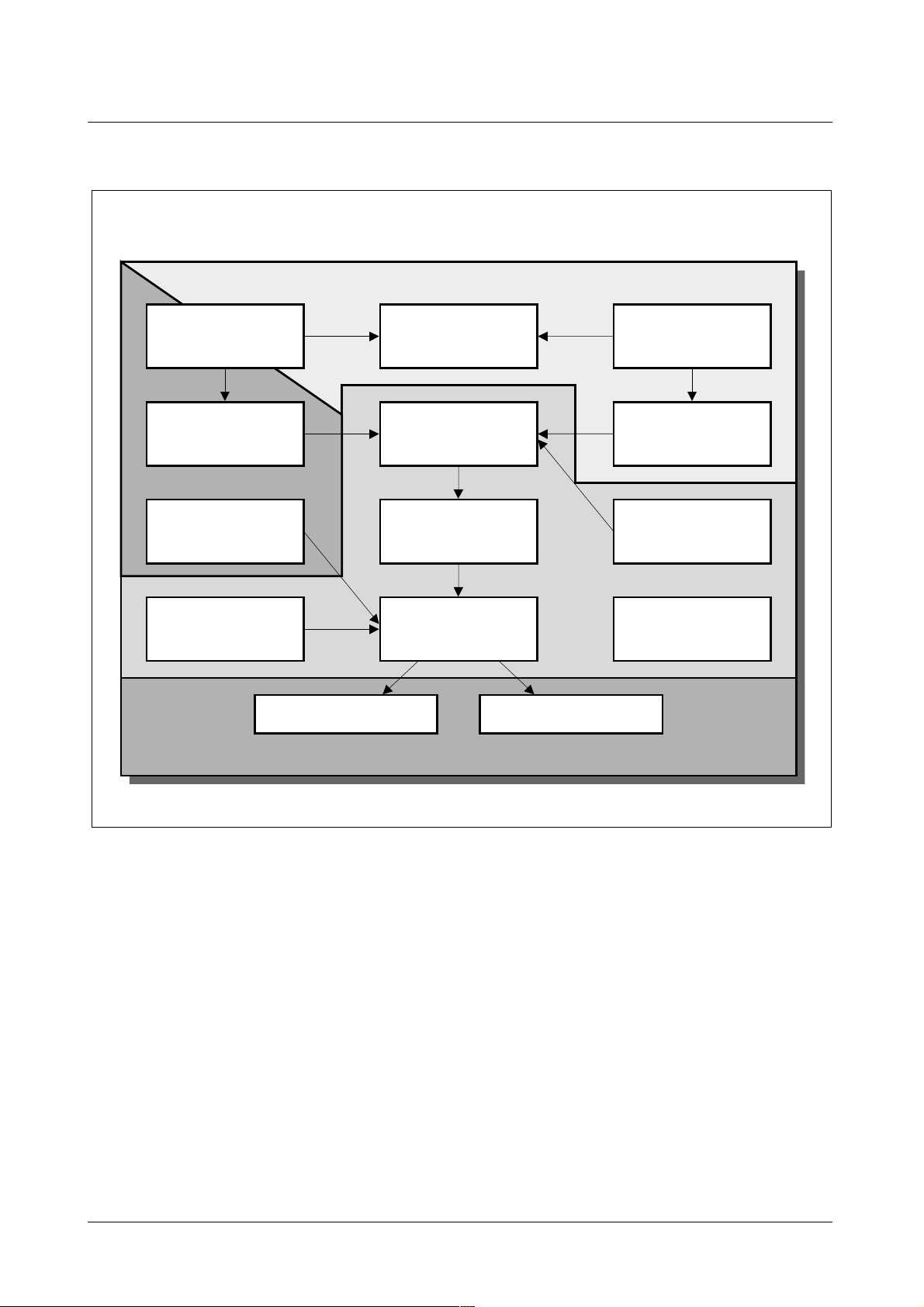
SIE-MATE Tool Concept:
Fast Prototyping on the PC
User Interface
Object Editor
Converter Display data
info M2 formatted data,
Object Library Manager
Dedicated
M2 Libraries
New Tool Generation
User Interface
Simulator
C Compiler
Object Code
C166-Available
Overview
Events and
Action Editor
C Code
Generator
C Sources
RTOS
Embedded System M2
M2 - the 16 Bit MC, TTX/EPG/TeleWeb, High End OSD Engine
Figure 1-1 M2 Tool Flow
Linker/Locator
PC Simulator + EVA Board
Debugging
UEB11114
1 - 5 Micronas
Page 17

SDA 6000 PRELIMINARY DATA SHEET
Version 2.1
Standard Tool Chain
For the M2 software development (documentation, coding, debugging and test) the
Infineon C166 microcontroller family standard tools can be used: These are ASCII editor,
structogram editor, compiler, assembler, linker. Debugging is supported by low-priced
ROM-Monitor debuggers or the OCDS (On Chip Debug Support) debugger.
M2 Dedicated Tools
Special tools are primarily available for platform independent M2 software development
and secondly to generate data and control code for the M2 graphical user interface (GDI)
without having knowledge of M2 hardware. These are:
• Display Generator Simulator
• Teletext Data Slicer Simulator
• GDI (Graphical Device Interface)
• Teletext Decoder and Display Software for Level 1.5 and Level 2.5
• Mate Display Builder for management, editing, handling and generation of all
necessary data to display OSD’s
• Evaluation Board Simulator to connect a C166 EVA Board to the M2 simulation
Overview
The M2 software is written in ANSI-C to fulfil the platform independent development. The
ported software is code and runtime optimized. The layers of the modular architecture
are separated by application program interfaces which ensure independent handling of
the modules.
1 - 6 Micronas
Page 18
SDA 6000 PRELIMINARY DATA SHEET
Version 2.1
Overview
Teletext Decoder with Embedded 16-bit Controller
M2
Version 2.1 CMOS
1.1 Features
General
• Level 1.5, 2.5, 3.5 WST Display Compatible
• Fast External Bus Interface for SDRAM (Up to
8 MByte) and ROM or Flash-ROM (Up to 4 MByte)
• Embedded General Purpose 16 Bit CPU (Also used
as TV-System Controller, C16x Compatible)
• Display Generation Based on Pixel Memory
• Program Code also Executable From External
SDRAM
• Embedded Refresh Controller for External SDRAM
• Enhanced Programmable Low Power Modes
• Single 6 MHz Crystal Oscillator
• Multinorm H/V-Display Synchronization in Master or Slave Mode
• Free Programmable Pixel Clock from 10 MHz to 50 MHz
• Pixel Clock Independent from CPU Clock
⌠ 6 Bits RGB-DACs On-Chip
• 3
• Supply Voltage 2.5 and 3.3 V
• P-MQFP-128 Package
P-MQFP-128-2
Microcontroller Features
• 16-bit C166-CPU Kernel (C16x Compatible)
• 60 ns Instruction Cycle Time
• 2 KBytes Dual Ported IRAM
• 2 KBytes XRAM On-chip
• General Purpose Timer Units (GPT1 and GPT2).
• Asynchronous/Synchronous Serial Interface (ASC0) with IrDA Support. Full-duplex
Asynchronous Up To 2 MBaud or Half-duplex Synchronous up to 4.1 MBaud.
Type Package
SDA 6000 P-MQFP-128-2
1 - 7 Micronas
Page 19

SDA 6000 PRELIMINARY DATA SHEET
Version 2.1
Overview
• High-speed Synchronous Serial Interface (SSC). Full- and Half-duplex synchronous
up to 16.5 Mbaud
2
• 3 Independent, HW-supported Multi Master/Slave I
C Channels at 400 Kbit/s
• 16-Bit Watchdog Timer (WDT)
• Real Time Clock (RTC)
• On Chip Debug Support (OCDS)
• 4-Channel 8-bit A/D Converter
• 42 Multiple Purpose Ports
• 8 External Interrupts
• 33 Interrupt Nodes
Display Features
• OSD size from 0 to 2046 (0 to 1023) pixels in horizontal (vertical) direction
• Frame Buffer Based Display
• 2 HW Display Layers
• Support of Double Page Level 2.5 TTX in 100 Hz Systems
• Support of Transparency for both Layers Pixel by Pixel
• User Programmable Pixel Frequency from 10.0 MHz to 50 MHz
• Up to 65536 Displayable Colors in one Frame
• DMA Functionality
• Graphic Accelerator Functions (Draw Lines, Draw and Fill Rectangle, etc.)
• 1, 2, 4 or 8-bit Bitmaps (up to 256 out of 4096 colors)
• 12 bit/16 bit RGB Mode for Display of up to 65535 Colors
• HW-support for Proportional Characters
• HW-support for Italic Characters
• User Definable Character Fonts
• Fast Blanking and Contrast Reduction Output
Acquisition Features
• Two Independent Data Slicers (One Multistandard Slicer + one WSS-only Slicer)
• Parallel Multi-norm Slicing (TTX, VPS, WSS, CC, G+)
• Four Different Framing Codes Available
• Data Caption only Limited by available Memory
• Programmable VBI-buffer
• Full Channel Data Slicing Supported
• Fully Digital Signal Processing
• Noise Measurement and Controlled Noise Compensation
• Attenuation Measurement and Compensation
• Group Delay Measurement and Compensation
• Exact Decoding of Echo Disturbed Signals
1 - 8 Micronas
Page 20
SDA 6000 PRELIMINARY DATA SHEET
Version 2.1
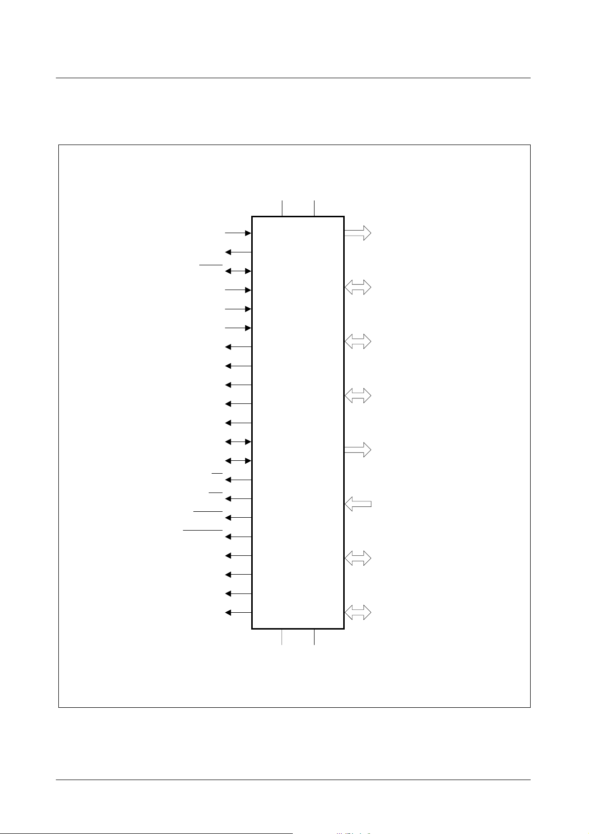
1.2 Logic Symbol
XTAL1
XTAL2
RSTIN
CVBS1A
CVBS1B
CVBS2
Overview
V
R
G
SS
V
DD(3.3 V)
Address
16 Bit
Data
16 Bit
Port 2
8 Bit
B
COR
BLANK
HSYNC
VSYNC
RD
WR
CSROM
CSSDRAM
MEMCLK
UDQM
LDQM
CLKEN
Port 3
15 Bit
M2
Port 4
6 Bit
Port 5
6 Bit
Port 6
7 Bit
JTAG
4 Bit
V
SS
V
DD(2.5 V)
UEL11115
Figure 1-2 Logic Symbol
1 - 9 Micronas
Page 21

Pin Description
Page 22

SDA 6000 PRELIMINARY DATA SHEET
Version 2.1
2 Pin Descriptions
Pin Descriptions
2 - 3 Micronas
Page 23
SDA 6000 PRELIMINARY DATA SHEET
Version 2.1
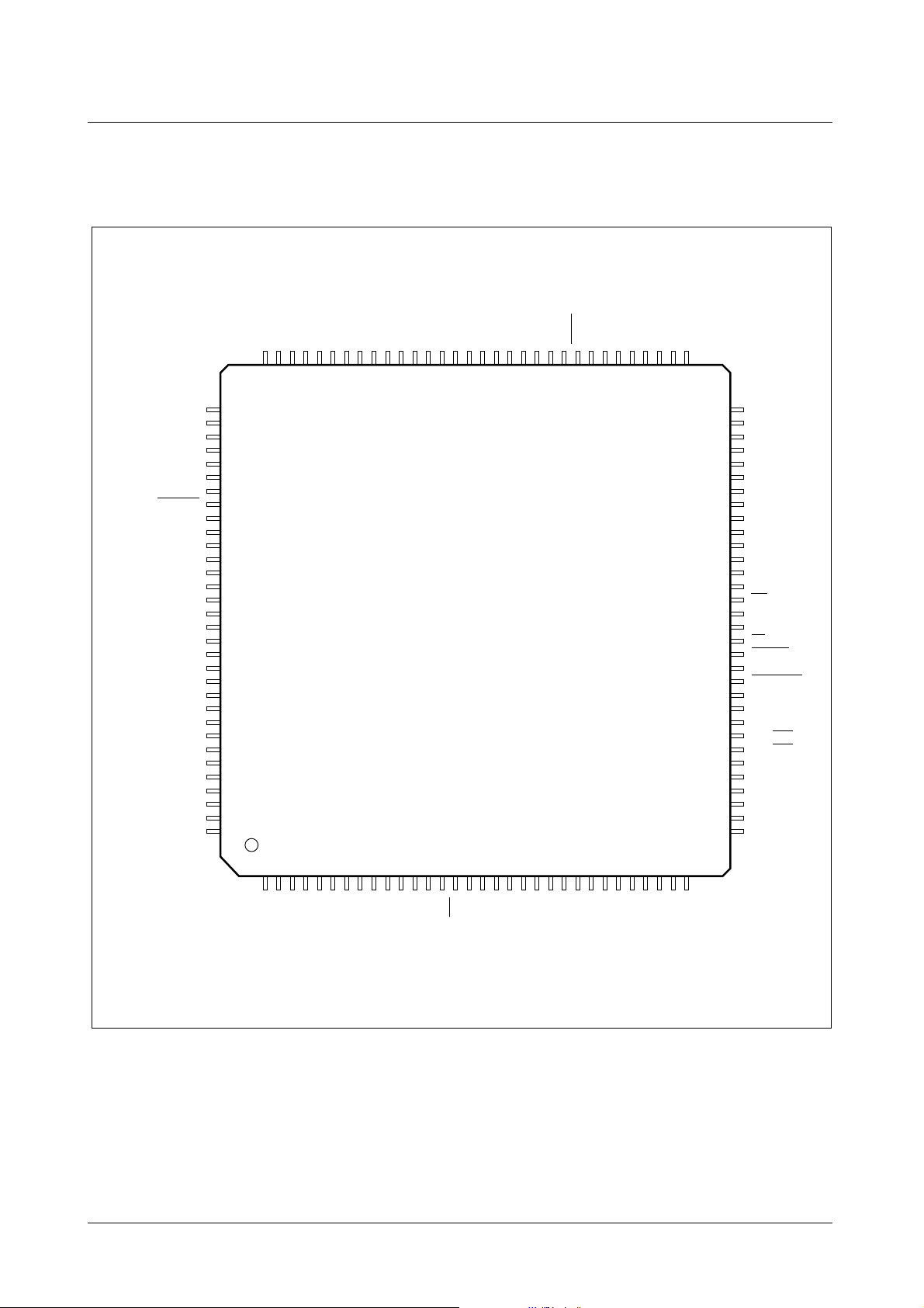
2.1 Pin Diagram (top view)
P-MQFP-128-2
DD25-2
P3.10
P3.11
P3.12
P3.13
P3.15
P5.14
P5.15
P6.0
P6.1
91
92
95
96
93
94
97 64
P6.2
98
P6.3
99 62
P6.4
100 61
P6.5
101 60
P6.6
VSYNC
HSYNC
COR/RSTOUT
BLANK/CORBLA
V
DD33-8
V
SS33-8
XTAL1
XTAL2
V
V
V
V
CVBS2
V
V
CVBS1B
CVBS1A
V
V
TMODE A4
102 59
103 58
104 57
105 56
106 55
107 54
108
109 52
110 51
SSA-1
111 50
DDA-1
112 49
R
113 48
G
114 47
B
115 46
SSA-2
116 45
DDA-2
117 44
118
SSA-3
119 42
DDA-3
120 41
121 40
122 39
SSA-4
123 38
DDA-4
124 37
P5.0
125 36
P5.1
126 35
P5.2
127 34
P5.3 A3
128
90
89
88
V
87
SS33-7
DD33-7
SS25-2
V
V
85
86
V
84
P3.9
83
P3.8
82
P3.7
81
P-MQFP-128-2
M2
P3.5
P3.6
79
80
P3.3
P3.4
78
77
P3.2
76
P3.0
P3.1
75
74
D11
RSTIN
72
73
D3
71
D4
70
Pin Descriptions
SS33-6
DD33-6
D12
D10
D2
V
V
68
67
66
65
63
53
43
33
69
D5
D9
D13
V
DD33-5
V
SS33-5
D1
D6
D8
D14
D0
D7
V
DD33-4
V
SS33-4
D15
WR
LDQM
UDQM
RD
CSROM
CLKEN
CSSDRAM
MEMCLK
V
DD33-3
V
SS33-3
A15/CAS
A14/RAS
A13
A0
A1
A2
2345678
1
TDI
TCK
TMS
P2.8
TDO
P2.9
P2.10
9
101112131415161718
SS33-1
P2.15
P2.14
V
DD33-1
V
P2.12
P2.11
P2.13
P4.3/A19
P4.2/A18
P4.4/A20
P4.5/CS3
20212223242526272829303132
19
A5
A9
A8
A6
SS25-1
DD25-1
V
V
P4.1/A17
A7
P4.0/A16
A10
A11
A12
SS33-2
V
V
DD33-2
UEP11116
Figure 2-1 Pin Configuration
2 - 4 Micronas
Page 24

SDA 6000 PRELIMINARY DATA SHEET
Version 2.1
Pin Descriptions
2.2 Pin Definitions and Functions
Table 2-1 Pin Definition and Functions
Pin
No.
37 A0 R0/C0 O Address bit (All addresses are word
36 A1 R1/C1 O Address bit/SDRAM address bit
35 A2 R2/C2 O Address bit/SDRAM address bit
34 A3 R3/C3 O Address bit/SDRAM address bit
33 A4 R4/C4 O Address bit/SDRAM address bit
27 A5 R5/C5 O Address bit/SDRAM address bit
26 A6 R6/C6 O Address bit/SDRAM address bit
24 A7 R7/C7 O Address bit/SDRAM address bit
Pin Name Second
Function
Dir. Function
addresses)/SDRAM Address bit
23 A8 R8 O Address bit/SDRAM address bit
25 A9 R9 O Address bit/SDRAM address bit
28 A10 R10 O Address bit/SDRAM address bit
29 A11 R11 O Address bit/SDRAM address bit
30 A12 R12 O Address bit/SDRAM address bit
38 A13 R13 O Address bit/SDRAM address bit
39 A14 RAS
40 A15 CAS
55 D0 – I/O Data bit
59 D1 – I/O Data bit
65 D2 – I/O Data bit
71 D3 – I/O Data bit
70 D4 – I/O Data bit
O Address bit/
Row address strobe for SDRAM access
O Address bit/
Column address strobe for SDRAM access
64 D5 – I/O Data bit
58 D6 – I/O Data bit
54 D7 – I/O Data bit
57 D8 – I/O Data bit
63 D9 – I/O Data bit
2 - 5 Micronas
Page 25
SDA 6000 PRELIMINARY DATA SHEET
Version 2.1
Table 2-1 Pin Definition and Functions (cont’d)
Pin
No.
67 D10 – I/O Data bit
72 D11 – I/O Data bit
66 D12 – I/O Data bit
62 D13 – I/O Data bit
56 D14 – I/O Data bit
51 D15 – I/O Data bit
47 RD
46 CSROM
44 CSSDRAM
Pin Name Second
Function
– O External memory read strobe for ROM. RD is
– O Chip select signal for ROM device
– O Chip select signal for SDRAM device
Dir. Function
activated for every external instruction or data
read access.
Pin Descriptions
43 MEMCLK – O Clock for SDRAM
45 CLKEN – O Enable for memory clock
50 WR
22 P4.0 A16 O General purpose output port/Address bit
19 P4.1 A17 O General purpose output port/Address bit
18 P4.2 A18 O General purpose output port/Address bit
17 P4.3 A19 O General purpose output port/Address bit
16 P4.4 A20 O General purpose output port/Address bit
15 P4.5 CS3 O General purpose output port/Chip select
49 LDQM – O Write disable for low byte
48 UDQM – O Write disable for high byte
109 XTAL2 – O Output of the oscillator amplifier circuit
108 XTAL1 – I Input of the oscillator amplifier circuit
73 RSTIN
– O Memory write strobe
signal for second external static memory
– I Reset input pin
121 CVBS1A – I CVBS signal inputs for full service data slicing
120 CVBS1B – I Ground for CVBS1A (differential input)
117 CVBS2 – I CVBS signal inputs for WSS data slicing
112 R – O Analog output for red channel
2 - 6 Micronas
Page 26

SDA 6000 PRELIMINARY DATA SHEET
Version 2.1
Pin Descriptions
Table 2-1 Pin Definition and Functions (cont’d)
Pin
No.
Pin Name Second
Function
Dir. Function
113 G – O Analog output for green channel
114 B – O Analog output for blue channel
104 COR RSTOUT O Output for contrast reduction/Reset output
105 BLANK CORBLA O Fast blanking signal/Three-level signal for
contrast reduction + fast blanking
103 HSYNC – I/O Horizontal sync In/output
102 VSYNC VCS I/O Vertical sync In/output/Composite sync output
5 P2.8 EX0IN I/O General purpose I/O port/External interrupt 0
6 P2.9 EX1IN I/O General purpose I/O port/External interrupt 1
7 P2.10 EX2IN I/O General purpose I/O port/External interrupt 2
8 P2.11 EX3IN I/O General purpose I/O port/External interrupt 3
9 P2.12 EX4IN I/O General purpose I/O port/External interrupt 4
10 P2.13 EX5IN I/O General purpose I/O port/External interrupt 5
11 P2.14 EX6IN I/O General purpose I/O port/External interrupt 6
12 P2.15 EX7IN I/O General purpose I/O port/External interrupt 7
2
74 P3.0 SCL0 I/O General purpose I/O port/I
75 P3.1 SDA0 I/O General purpose I/O port/I
C Bus clock line 0
2
C Bus data line 0
76 P3.2 CAPIN I/O General purpose I/O port/GPT2 register
CAPREL
77 P3.3 T3OUT I/O General purpose I/O port/GPT1 timer T3
toggle
78 P3.4 T3EUD I/O General purpose I/O port/GPT1 timer T3 ext.
up/down
79 P3.5 T4IN I/O General purpose I/O port/GPT1 timer T4 input
for count/gate/reload/capture
80 P3.6 T3IN I/O General purpose I/O port/GPT1 timer T3
count/gate input
81 P3.7 T2IN I/O General purpose I/O port/GPT1 timer T2 input
for count/gate/reload/capture
82 P3.8 MRST I/O General purpose I/O port/SSC master-
receiver/slave-transmit I/O
2 - 7 Micronas
Page 27

SDA 6000 PRELIMINARY DATA SHEET
Version 2.1
Pin Descriptions
Table 2-1 Pin Definition and Functions (cont’d)
Pin
No.
Pin Name Second
Function
Dir. Function
83 P3.9 MTSR I/O General purpose I/O port/SSC master-
transmit/slave-receiver O/I
88 P3.10 TxD0 I/O General purpose I/O port/ASC0 clock/data
output
89 P3.11 RxD0 I/O General purpose I/O port/ASC0 data input
(asynchronous) or I/O (synchronous.)
90 P3.12 – I/O General purpose I/O port
91 P3.13 SCLK I/O General purpose I/O port/SSC master clock
output/slave clock input
92 P3.15 – I/O General purpose I/O port
124 P5.0 AN.0 I General purpose I/O port/Analog input for
A/D-converter
125 P5.1 AN.1 I General purpose I/O port/Analog input for
A/D-converter
126 P5.2 AN.2 I General purpose I/O port/Analog input for
A/D-converter
127 P5.3 AN.3 I General purpose I/O port/Analog input for
A/D-converter
93 P5.14 T4EUD I/O General purpose I/O port/GPT1 timer T4
ext.up/down ctrl. input
94 P5.15 T2EUD I/O General purpose I/O port/GPT1 timer T2
ext.up/down ctrl. input
95 P6.0 TRIG_IN I/O General purpose I/O port/Trigger input-signal
for ‘On Chip Debug System’ (OCDS)
96 P6.1 TRIG_OUT I/O General purpose I/O port/Trigger output-
signal for ‘On Chip Debug System’ (OCDS)
97 P6.2 – I/O General purpose I/O port
2
98 P6.3 SCL1 I/O General purpose I/O port/I
99 P6.4 SDA1 I/O General purpose I/O port/I
C bus clock line 1
2
C bus data line 1
100 P6.5 – I/O General purpose I/O port
2
101 P6.6 SDA2 I/O General purpose I/O port/I
C bus data line 2
1TCK – I Clock for JTAG interface
3TDI – I Data input for JTAG interface
2 - 8 Micronas
Page 28

SDA 6000 PRELIMINARY DATA SHEET
Version 2.1
Pin Descriptions
Table 2-1 Pin Definition and Functions (cont’d)
Pin
No.
Pin Name Second
Function
Dir. Function
4TDO – O Data output for JTAG interface
2TMS – I Control signal for JTAG interface
128 TMODE – I Testmode pin
110 V
111
115,
SSA-1
V
DDA-1
V
SSA2-4
– S Analog ground
– S Analog power (for PLL and DAC) (2.5 V)
– S Analog ground
1)
118,
122
116,
V
DDA2-4
– S Analog power (for ADCs) (2.5 V)
119,
123
20, 86
21, 87
V
SS25 1-2
V
DD25 1-2
– S Digital ground (for digital core)
– S Digital power (for digital core) (2.5 V)
13, 31,
V
SS33 1-8
– S Digital ground for pads
41, 52,
60, 68,
84,
107
14, 32,
V
DD33 1-8
– S Digital power (for pads) (3.3 V)
42, 53,
61, 69,
85,
106
1)
(Must be kept to “0” in application.)
2 - 9 Micronas
Page 29

Architectural Overview
Page 30
SDA 6000 PRELIMINARY DATA SHEET
Version 2.1
3 Architectural Overview
XTAL
OSC
(6 MHz)
PEC
Interrupt Controller
16
Data
RAM
Internal
2 Kbyte
16
DataInstr./Data32
C166
CPU-Core
36 nodes (8 ext.)
Architectural Overview
4
OCDS
GPT2
JTAG
RTC Watchdog
C
2
Ι
T5
T6
7
Port 6
UEB10716
ACQ
Slicer1
CVBS1
CVBS2
Slicer2
-Cache
Ι
AMI
Boot
ROM
16
16...21
16
External
Addr.
Bus
Interface
D-Cache
16
16
Data
16 X-BUS Instr./Data
XRAM
2 Kbyte
SRUGA
T2
GPT1
4-
T3
T4
SPI
ASC SSC
USART
7-bit
ADC
Channel
D-Sync
FIFO
Port 5 Port 3 Port 2 Port 4
DAC
3 x 6 Bit
6 15 8 8
HV
3
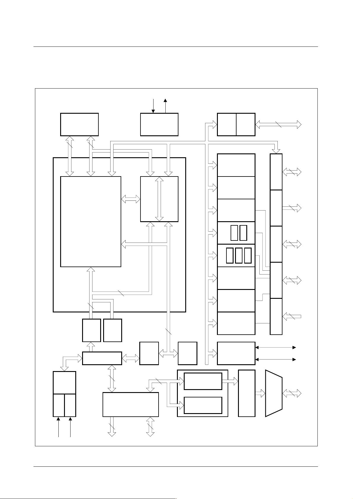
Figure 3-1 M2 Top Level Block Diagram
3 - 3 Micronas
Page 31

SDA 6000 PRELIMINARY DATA SHEET
Version 2.1
The architecture of M2 comprises of a 16-bit microcontroller which is derived from the
well known Infineon Technologies C16x controller family. Due to the core philosophy of
M2, the architecture of the CPU core is the same as described in other Infineon
Technologies C16x derivatives.
The CPU, with its peripherals, can be used on one hand to perform all TV controlling
tasks, and on the other hand to process the data, sliced by the slicer, and the acquisition
unit according to the TTX standard. Furthermore it is used to generate an “instruction list”
for the graphic accelerator which supports the CPU by generating the display.
M2 has integrated two digital slicers for two independent CVBS signals. One slicer is
used to capture the data (e.g. Teletext or EPG) from the main channel, the other slicer
can be used to slice the WSS information from a different channel, which is helpful e.g.
to support PIP applications in 16:9 TVs. Both slicers separate the data from the analog
signal and perform the bit synchronization and framing code selection before the data is
stored in a programmable VBI buffer in the external RAM. Capturing and storing the raw
data in the RAM does not need any CPU power.
M2’s display concept has improved in comparison to the common known state of the art
Teletext-ICs. The display concept is based on a pixel orientated attribute definition
instead of the former character orientated attribute definition.
Architectural Overview
For the processing of this new pixel based attribute definition the display generator
architecture is divided in two subblocks: the graphic accelerator (GA) and the screen
refresh unit (SRU).
The graphic accelerator is used to modify the frame buffer. From an abstract point of
view, the graphic accelerator is a DMA which is optimized for OSD functionality, so e.g.
bitmaps can be copied to the frame buffer. The graphic accelerator is used to draw
rectangles, parallelograms, horizontal, vertical and diagonal lines. The user does not
need to access the graphic accelerator directly, thanks to an easy to handle SW-GDI
function which is available with the M2 hardware.
The DMA functionality of the display generator (DG) supports the pixel transfer between
any address of entire external memory. The teletext and graphic capabilities can be used
simultaneously, so that M2 can combine teletext information with e.g. background
images and advanced high resolution OSD graphics.
M2 uses the frame buffer located in external memory so every bitmap can be placed at
any location on the screen. The contents of the frame buffer does not have to be set up
in real time. The duration of the set up of the screen depends on the contents of the
displayed information.
M2 supports two hardware display layers. To refresh the screen the M2 reads and mixes
two independent pixel sources simultaneously.
Different formats of the pixels which are part of different applications (e.g. Teletext
formats, 12-bit RGB or 16-bit RGB values) can be stored in the same frame buffer at the
same time.
3 - 4 Micronas
Page 32

SDA 6000 PRELIMINARY DATA SHEET
Version 2.1
Architectural Overview
The screen refresh unit is used to read the frame buffer pixel by pixel in real time and to
process the transparency and RGB data. A color look up table (CLUT) can be used to
get the RGB data of the current pixel. Afterwards the RGB data is transferred to the D/A
converter. The blank signal and contrast reduction signal (COR) is also processed for
each pixel by the SRU and transferred to the corresponding output pins.
The pixel, line and field frequencies are widely programmable so that the sync system
can be used from low end 50 Hz to high end 100 HZ TV applications as well as for any
other standard.
The on chip clock system provides the M2 with its basic clock signals. Independent
clock domains are provided for the embedded controller, the bus interface and the
display system. The pixel clock can vary between 10 MHz and 50 MHz.
Due to the unified memory architecture of M2, a new bus concept is implemented. An
arbiter handles the bus requests from the different request sources. These are:
• Slicer 1 requests (normally used as a TTX slicer)
• Slicer 2 requests (used as a WSS slicer)
• Graphic accelerator requests
• Screen refresh unit requests
• Data requests from the CPU via XBUS
• Instruction requests via the CPU program bus
For exploiting the full computational power of the controller core the code of time critical
routines can be stored in one bank of the external SDRAM separated from all display
information (frame buffer, character set etc.). An instruction cache (I-CACHE) is used
for buffering instruction words in order to minimize the probability of wait states to occur
when the microcontroller is interfering with the display generator (DG) for access rights
to the external memory devices. The data cache (D-CACHE) serves for operand reads
and writes via the XBUS from/to external memory devices.
The external bus interface (EBI) features interleaved access cycles to one or two static
external memory devices (ROM, Flash-ROM or SRAM) with a total maximum size of
4 MByte and one PC100 compliant (Intel standard) SDRAM device (16 MBit organized
as 2 memory banks or 64 MBit organized as 4 memory banks).
2
For TV controlling tasks M2 provides three serial interfaces (I
C, ASC, SSC), two general
purpose timers, (GPT1, GPT2), a real time clock (RTC), a watch dog timer (WDT), an A/
D converter and eight external interrupts.
3 - 5 Micronas
Page 33

C16X Microcontroller
Page 34

SDA 6000 PRELIMINARY DATA SHEET
Version 2.1
4 C16X Microcontroller
C16X Microcontroller
4 - 3 Micronas
Page 35

SDA 6000 PRELIMINARY DATA SHEET
Version 2.1
C16X Microcontroller
4.1 Overview
M2’s microcontroller and its peripherals are based on a Cell-Based Core (CBC) which is
compatible to the well known C166 architecture.
In M2, the CPU and its peripherals are generally clocked with 33.33 MHz which results
in an instruction cycle time of 60 ns. The implementation of the microcontroller within M2
deviates from other known C16x derivates since the controller’s XBUS is not used as the
external bus. All external access cycles of the microcontroller, the display generator and
the acquisition unit are performed via a high performance time interlocking SDRAM bus.
The external bus interface (EBI) manages the arbitration procedure for access cycles to
the external synchronous DRAM in parallel to an external static memory (ROM or
FLASH; for more details refer to Chapter 4.4).
Due to the realtime critical bus bandwidth requirements of the display generator,
unpredictable wait-states for the controller may occur. These wait-states do not destroy
the overall average system performance, because they are mostly buffered by the CPU
related instruction and data buffers. Nevertheless they can influence, for example, the
worst disconnection response time.
Emulation is now performed by an on-chip debug module which can be accessed by a
JTAG interface.
The following microcontroller peripherals are implemented:
• 2 KByte IRAM (System RAM)
• 2 KByte XRAM (XBUS located)
• 32 Interrupt Nodes
• General Purpose Timer Units (GPT1 and GPT2)
• Real Time Clock (RTC)
• Asynchronous/Synchronous Serial Interface (ASC0)
• High-Speed Synchronous Serial Interface (SSC)
2
C Bus Interface (I2C)
• I
• 4-Channel 8-bit A/D Converter (ADC)
• Watchdog Timer (WDT)
• On-Chip Debug Support Module (OCDS)
• 42 Multiple Purpose Ports
Central Processing Unit
The CPU executes the C166 instruction set (with the extensions of the C167 products).
Its main features are the following:
• 4-stage pipeline (Fetch, Decode, Execute and Write-Back).
• 16
⌠ 16-bit General Purpose Registers
• 16-bit Arithmetic and Logic Unit
• Barrel shifter
• Bit processing capability
4 - 4 Micronas
Page 36

SDA 6000 PRELIMINARY DATA SHEET
Version 2.1
• Hardware support for multiply and divide instructions
Internal RAM (IRAM)
The internal dual-port RAM is the physical support for the General Purpose Registers,
the system stack and the PEC pointers. Due to its close connections with the CPU, the
internal RAM provides fast access to these resources. As the GPR bank can be mapped
anywhere in the internal RAM through a base pointer (Context Pointer CP), fast context
switching is allowed. The internal RAM is mapped in the memory space of the CPU and
can be used also to store user variables or code.
Interrupt Controller
Up to 32 interrupt sources can be managed by the Interrupt Controller through a multiple
priority system which provides the user with the ability to customize the interrupt
handling.
The interrupt system of M2 includes a Peripheral Event Controller (PEC). This processor
performs single-cycle interrupt-driven byte or word transfers between any two locations
in the entire memory space of M2.
C16X Microcontroller
In M2, the PEC functionalities are extended by the External PEC which allows an
external device to trigger a PEC transfer while providing the source and destination
pointers. New features also include the packet transfer mode and the channel link mode.
Besides user interrupts, the Interrupt Controller provides mechanisms to process
exceptions or error conditions, so-called “hardware traps”, that arise during program
execution.
System Control Unit
M2’s System Control Unit (CSCU) is used to control system specific tasks such as reset
control or power management within an on-chip system built around the core. The power
management features of the CSCU provide effective means to realize standby
conditions for the system with an optimum balance between power reduction, peripheral
operation and system functionality. The CSCU also provides an interface to the Clock
Generation Unit (CGU) and is able to control the operation of the Real Time Clock (RTC).
The CSCU includes the following functions:
• System configuration control
• Reset sequence control
• External interrupt and frequency output control
• Watchdog timer module
• General XBUS peripherals control
• Power management additional to the standard Idle and Power Down modes
• Control interface for Clock Generation Unit
• Identification register block for chip and CSCU identification
4 - 5 Micronas
Page 37

SDA 6000 PRELIMINARY DATA SHEET
Version 2.1
OCDS
The On-Chip Debug System allows the detection of specific events during user program
execution through software and hardware breakpoints. An additional communication
module allows communication between the OCDS and an external debugger, through a
standard JTAG port. This communication is performed in parallel to program execution.
C16X Microcontroller
4 - 6 Micronas
Page 38

SDA 6000 PRELIMINARY DATA SHEET
Version 2.1
C16X Microcontroller
4.2 Memory Organization
In normal operation mode the memory space of the CPU is configured in a “Von
Neumann” architecture. This means that code and data are accessed within the same
memory areas, i. e. external memory, internal controller memory (IRAM), the address
2
areas for integrated XBUS peripherals (I
special function register areas (SFR, ESFR) are mapped into one common address
space of 16 MBytes. This address space is arranged as 256 segments of 64 KBytes
each and each segment is again subdivided into four data pages of 16 KBytes each.
All internal memory areas and the address space of the integrated XBUS peripherals are
mapped to segment 0. Code and data may be stored in any part of the memory, except
for the SFR blocks, which can not be used for instructions. Despite this equivalence of
code and data, proper partitioning is necessary to make use of the full bandwidth of the
memory system.
The integrated C16x controller communicates via 2 busses with the memory interface.
In normal operation mode access to segments 00H to 41H (excluding internal memory
areas) is mapped to the read only program memory bus (PMBUS), whereas access to
segments 42
to FFH is mapped to the XBUS. In bootstrap loader mode (BSLMode)
H
instruction fetches to external memory areas via PMBUS are redirected to the internal
bootstrap loader ROM (BSLROM). Operand (data) accesses remain unchanged.
C, internal XBUS memory (XRAM)) and the
The PMBUS is connected to the instruction cache (ICACHE) which operates as readahead FIFO (see Figure 4-1). The data cache (DCACHE) which is connected to the
XBUS holds a maximum of 4 words corresponding to one SDRAM burst. Accesses of
DCACHE, ICACHE and the acquisition unit (ACQ) are joined within the acquisition
memory interface (AMI) and directed to the external bus interface (EBI). Redirections via
ESFR REDIR (instruction fetches only) and ESFR REDIR1 are done in the AMI (see
Chapter 4.5.1). The EBI joins AMI and display generator (DG) accesses and reads data
from or writes data to the external static and dynamic memory devices (see Chapter 4.5
for further information). In case of cache miss wait states are inserted until the data is
ready. IRAM, XRAM and the special function register areas can be accessed without
wait states.
4 - 7 Micronas
Page 39

SDA 6000 PRELIMINARY DATA SHEET
Version 2.1
External M2
Memory
DG
SDRAM
Boot ROM
ROM1
ROM2
EBI
AMI
ICACHE
DCACHE
ACQ
C16X Microcontroller
PMBUS
C16X
XBUS
UED11214
Figure 4-1 M2 Memory Path Block Diagram
All memory locations are byte and word readable. The internal memories (IRAM, XRAM)
and the external dynamic memory (SDRAM) are byte and word writable, but external
static memory is only word writable. Bytes are stored at even or odd byte addresses.
Words are stored in ascending memory locations, with the low byte at an even byte
address being followed by the high byte at the next odd byte address. Double words
(instructions only) are stored in ascending memory locations as two subsequent words.
Single bits are always stored in the specific bit position at a word address. Bit position 0
is the least significant bit of the byte at an even byte address and bit position 15 is the
most significant bit of the byte at the next odd byte address. Bit addressing is supported
by a part of the special function registers, a part of the IRAM and the general purpose
registers (GPRs).
4 - 8 Micronas
Page 40

SDA 6000 PRELIMINARY DATA SHEET
Version 2.1
C16X Microcontroller
Figure 4-2 Storage of Words, Byte and Bits in a Byte Organized Memory
Note: Byte units forming a single word or a double word must always be stored within
the same physical (internal, external, ROM, RAM) and organizational (page,
segment) memory area.
4 - 9 Micronas
Page 41

SDA 6000 PRELIMINARY DATA SHEET
Version 2.1
C16X Microcontroller
4.3 On-Chip Microcontroller RAM and SFR Area
The IRAM/SFR area is located within data page 3, and provides access to 2 KByte of
dual ported IRAM and two 512 Byte blocks of Special Function Registers (SFRs).
The internal RAM (IRAM) serves several purposes:
• System Stack (Programmable Size)
• General Purpose Register Banks (GPRs)
• Source and Destination Pointers for the Peripheral Event Controller (PEC)
• Variable and other data storage, or
• Code storage
Segment 0
64 Kbytes
RAM / SFR Area
2
Ι
C
XRAM
00’FFFF
00’F000
00’E800
00’E000
H
H
H
Page 3
H
RAM / SFR Area
4 Kbytes
SFR Area
00’FFFF
00’FE00
H
H
00’C000
00’8000
00’4000
H
H
H
Page 2
Page 1
Page 0
2 Kbyte
IRAM
Reserved
00’FA00
00’F600
00’F200
H
H
H
ESFR Area
00’0000
H
00’F000
UED11213
H
Figure 4-3 Internal RAM Areas and SFR Areas
Note: The upper 256 bytes of SFR area, ESFR area and IRAM are bit-addressable (see
shaded blocks in Figure 4-3).
4 - 10 Micronas
Page 42

SDA 6000 PRELIMINARY DATA SHEET
Version 2.1
C16X Microcontroller
Code accesses are always made through even byte addresses. The highest possible
code storage location in the IRAM is either 00’FDFE
00’FDFC
for double word instructions. The respective location must contain a branch
H
for single word instructions, or
H
instruction (unconditional), because sequential boundary crossings from IRAM to the
SFR area are not supported and cause erroneous results.
Any word and byte data in the IRAM can be accessed via indirect or long 16-bit
addressing modes if the selected DPP register points to page 3. Any word data access
is made through an even byte address. The highest possible word data storage location
in the IRAM is 00’FDFE
. For PEC data transfers, the IRAM can be accessed
H
independent of the contents of the DPP registers via the PEC source and destination
pointers.
The upper 256 Byte of the IRAM (00’FD00
through 00’FDFFH) and the GPRs of the
H
current bank are provided for single bit storage, and thus they are bit addressable.
4.3.1 System Stack
The system stack may be defined within the IRAM. The size of the system stack is
controlled by bit field STKSZ in the SYSCON register (see table below).
<STKSZ> Stack Size
Internal RAM Addresses (Words)
(Words)
0 0 0
0 0 1
0 1 0
0 1 1
1 0 0
1 0 1
1 1 0
1 1 1
B
B
B
B
B
B
B
B
256 00’FBFEH… 00’FA00H (Default after Reset)
128 00’FBFEH… 00’FB00
64 00’FBFEH… 00’FB80
32 00’FBFEH… 00’FBC0
512 00’FBFEH… 00’F800
H
H
H
H
– Reserved. Do not use this combination.
– Reserved. Do not use this combination.
1024 00’FDFEH… 00’F600H (Note: No circular stack)
For all system stack operations, the IRAM is accessed via the Stack Pointer (SP)
register. The stack grows downward from higher to lower RAM address locations. Only
word accesses are supported by the system stack. A stack overflow (STKOV) and a
stack underflow (STKUN) register are provided to control the lower and upper limits of
the selected stack area. These two stack boundary registers can be used not only for
protection against data destruction, but also to implement flushing and filling a circular
stack with a hardware supported system stack (except for option ‘111’).
4 - 11 Micronas
Page 43

SDA 6000 PRELIMINARY DATA SHEET
Version 2.1
C16X Microcontroller
4.3.2 General Purpose Registers
The General Purpose Registers (GPRs) use a block of 16 consecutive words within the
IRAM. The Context Pointer (CP) register determines the base address of the currently
active register bank. This register bank may consist of up to 16 word GPRs (R0, R1, …,
R15) and/or of up to 16 byte GPRs (RL0, RH0, …, RL7, RH7). The sixteen byte GPRs
are mapped onto the first eight word GPRs (see Table 4-1).
In contrast to the system stack, a register bank grows from lower towards higher address
locations and occupies a maximum space of 32 Byte. The GPRs are accessed via short
2-, 4- or 8-bit addressing modes using the Context Pointer (CP) register as a base
address (independent of the current DPP register contents). In addition, each bit in the
currently active register bank can be accessed individually.
Table 4-1 Mapping of General Purpose Registers to RAM Addresses
Internal RAM
Address
<CP> + 1E
<CP> + 1C
<CP> + 1A
H
H
H
Byte Registers Word Register
– R15
– R14
– R13
<CP> + 18
<CP> + 16
<CP> + 14
<CP> + 12
<CP> + 10
<CP> + 0E
<CP> + 0C
<CP> + 0A
<CP> + 08
<CP> + 06
<CP> + 04
<CP> + 02
<CP> + 00
H
H
H
H
H
H
H
H
H
H
H
H
H
– R12
– R11
– R10
– R9
– R8
RH7 RL7 R7
RH6 RL6 R6
RH5 RL5 R5
RH4 RL4 R4
RH3 RL3 R3
RH2 RL2 R2
RH1 RL1 R1
RH0 RL0 R0
M2 supports fast register bank (context) switching. Multiple register banks can physically
exist within the IRAM at the same time. However, only the register bank selected by the
Context Pointer register (CP) is active at a given time. Selecting a new active register
bank is simply done by updating the CP register. A particular Switch Context (SCXT)
instruction performs register bank switching and automatically saves the previous
4 - 12 Micronas
Page 44

SDA 6000 PRELIMINARY DATA SHEET
Version 2.1
C16X Microcontroller
context. The number of implemented register banks (arbitrary sizes) is only limited by the
size of the available internal RAM.
4.3.3 PEC Source and Destination Pointers
The 16 word locations in the IRAM from 00’FCE0H to 00’FCFEH (just below the bitaddressable section) are provided as source and destination offset address pointers for
data transfers on the eight PEC channels. Each channel uses a pair of pointers stored
in two subsequent word locations, with the source pointer (SRCPx) on the lower and the
destination pointer (DSTPx) on the higher word address (x = 7 … 0). In M2, these
pointers are used to specify the address offset within the segment, and the destination /
source segment numbers are specified in designated SFRs (see Chapter 5.2).
00’FCFE
00’FD00
H
DSTP7
00’FCFE
H
H
00’FCFC
00’FCE2
00’FCE0
H
H
H
SRCP7
PEC
Source
and
Destination
Pointers
DSTP0
SRCP0
Internal
RAM
MCD02266
00’FCE0
00’FDDE
00’F600
00’F5FE
H
H
H
H
Figure 4-4 Location of the PEC Pointers
Whenever a PEC data transfer is performed, the pair of source and destination pointers,
which is selected by the specified PEC channel number, is accessed independent of the
current DPP register contents; the locations referred to by these pointers are also
accessed independent of the current DPP register contents. If a PEC channel is not
used, the corresponding pointer locations are available and can be used for word or byte
data storage.
4 - 13 Micronas
Page 45

SDA 6000 PRELIMINARY DATA SHEET
Version 2.1
C16X Microcontroller
4.3.4 Special Function Registers
The so-called Special Function Registers (SFRs) are provided to control internal
functions of M2 (CPU, bus interface, Interrupt Controller, OCDS) or peripherals
connected to the Peripheral Bus. These SFRs are arranged within two areas of
512 Bytes each. The first register block, the SFR area, is located in the 512 Bytes above
the internal RAM (00’FFFF
(ESFR) area, is located in the 512 Bytes below the IRAM (00’F1FF
Special function registers can be addressed via indirect and long 16-bit addressing
modes. Using an 8-bit offset together with an implicit base address allows word SFRs
and their respective low bytes to be addressed. However, this does not work for the
respective high bytes!
Note: Writing to any byte of an SFR causes the non-addressed complementary byte to
be cleared!
The upper half of each register block is bit-addressable, so the respective control/status
bits can directly be modified or checked using bit addressing.
When accessing registers in the ESFR area using 8-bit addresses or direct bit
addressing, an Extend Register (EXTR) instruction is first required to switch the short
addressing mechanism from the standard SFR area to the Extended SFR area. This is
not required for 16-bit and indirect addresses. The GPRs R15 … R0 are duplicated, i.e.
they are accessible within both register blocks via short 2-, 4- or 8-bit addresses without
switching.
… 00’FE00H); the second register block, the Extended SFR
H
… 00’F000H).
H
ESFR_SWITCH_EXAMPLE:
EXTR #4 ;Switch to ESFR area for next 4 instr.
MOV ODP2, #data16 ;ODP2 uses 8-bit reg addressing
BFLDL DP6, #mask, #data8 ;Bit addressing for bit fields
BSET DP1H.7 ;Bit addressing for single bits
MOV T8REL, R1 ;T8REL uses 16-bit mem address,
;R1 is duplicated into the ESFR space
;(EXTR is not required for this access)
;---- ;------------------- ;The scope of the EXTR #4 instruction…
; … ends here!
MOV T8REL, R1 ;T8REL uses 16-bit mem address,
;R1 is accessed via the SFR space
In order to minimize the use of the EXTR instructions the ESFR area primarily holds
registers which are required mainly for initialization and mode selection. Registers that
need to be accessed frequently are allocated, wherever possible, to the standard SFR
area.
4 - 14 Micronas
Page 46

SDA 6000 PRELIMINARY DATA SHEET
Version 2.1
Note: The tools are equipped to monitor accesses to the ESFR area and will
automatically insert EXTR instructions or issue a warning in case of missing or
excessive EXTR instructions.
C16X Microcontroller
4 - 15 Micronas
Page 47

SDA 6000 PRELIMINARY DATA SHEET
Version 2.1
C16X Microcontroller
4.4 External Memory
M2 provides an external bus interface (EBI) to access an external SDRAM, together with
an external static memory device (ROM or SRAM). To optimize the overall system
performance, access to both memory types is interlocked. Because of high performance
requirements M2 provides only one bus type (Demultiplexed 16-bit Bus). Depending on
the reset configuration (refer to Chapter 6.1) an external ROM/SRAM size from
128 KByte up to 4 MByte can be chosen. Although external addresses (represented by
pins A0 … A20) are always word addresses, byte accesses to the SDRAM are possible
by using mask signals LDQM and UDQM.
4.4.1 SDRAM
PC SDRAM compliant (Intel standard) memory devices with 2 or 8 MByte and a
minimum clock period of 10 ns (latency 3) may be connected to M2’s external memory
bus.
Supported data organizations are given below:
Memory Size # SDRAM
Banks
# Bank
Addresses
# Row
Addresses
# Column
Addresses
2 MByte21118
8 MByte42128
The external SDRAM connected to M2 is a multifunctional, byte or word addressable
device which can be used for frame buffers, character sets, pixel graphics, acquisitions,
microcontroller workspace and any other data storage purposes.
Using a 100 MHz external memory bus the theoretical optimum memory bandwidth is
limited to 200 MByte/s. In order to keep the sustainable memory bandwidth as close to
the optimum as possible, the bank oriented architecture of SDRAM devices has to be
exploited. Basically, display related information should be separated from controller
related data items.
The following allocation is recommended for a 2 bank, 2 MByte device:
• “Display Bank”: Both Frame Buffers, Character Set, Pixel Graphic, Graphic
Accelerator Instructions (GAI), Application Data (i.e. TTX, EPG, …)
• “Controller Bank”: Instruction Code, VBI-buffer, Application Data (i.e. TTX, EPG, …)
The suggested allocation leads to best performance results since it reduces the number
of time consuming row commands on the SDRAM.
4.4.2 External Static Memory Devices
M2 supports access to external ROM, Flash ROM and SRAM devices which provide a
read cycle time
4 - 16 Micronas
t
< 120 ns. Only 16-bit word access is supported. The maximum
RC
Page 48

SDA 6000 PRELIMINARY DATA SHEET
Version 2.1
memory size is limited by the number of external address lines. Up to 21 external
address lines are configurable, thus devices providing up to 4 MByte of static external
memory can be connected to M2.
C16X Microcontroller
4 - 17 Micronas
Page 49

SDA 6000 PRELIMINARY DATA SHEET
Version 2.1
C16X Microcontroller
4.5 External Bus Interface (EBI).
The EBI handles access channels to four SDRAM banks within one SDRAM device and
up to two static memory devices at 100 MHz. (For lower requirements the clock
frequency can be reduced to 66 MHz, refer to Chapter 8). A maximum of three external
memory devices is supported.
Figure 4-5 shows the possible configurations.
2...8 MByte
SDRAM
(2...4 banks)
ROM
or
Flash-ROM
128 KByte...4 MByte 128 KByte...4 MByte
ROM
or
Flash-ROM
M2
UEB11118
Figure 4-5 External Memory Configuration
The interlocking execution of access cycles to different memory modules is supported.
All external SDRAM access cycles must be executed with a pre-defined burst length
BL = 4 and latency 3. Write access cycles, which modify less than four SDRAM
locations, are achieved by activating mask control signals L/UDQM.
The integrated refresh controller of the EBI checks for the compliance of refresh periods
and executes refresh operations on the SDRAM devices. The configuration of different
external SDRAM types can be controlled by a special SW driver as well as refresh
modes and power down features. The microcontroller and the acquisition unit use a
common interface to the EBI. A separate connection to the EBI is provided for the display
generator. The EBI performs an arbitration procedure for granting right access to either
of the request sources. But granting right access to one source does not exclude
requests initiated by the other source from being served. A maximum of two access
requests from a source may be served consecutively if the other source is addressing
an SDRAM location. Up to four consecutive access cycles from the same source are
served if the other source is addressing an external ROM device.
The following figures show typical timing diagrams that may be observed on the external
bus. The first figure presents the interlocked execution of access cycles to the external
ROM and a SDRAM device. The other figure resumes the situation when both sources
4 - 18 Micronas
Page 50

SDA 6000 PRELIMINARY DATA SHEET
Version 2.1
C16X Microcontroller
address locations are in different SDRAM banks. Detailed timings and the specification
of setup and hold conditions can be found in Chapter 14.
MEMCLK
CSSDRAM
Act
RAS
CAS
WR
A(21:0)
Read
ca
ROM_Adr
ra
Write
ra
SDRAM Data
D(15:0)
CSROM
RD
ROM Data
Figure 4-6 Interlocked Access Cycles to ROM and SDRAM
UET11119
4 - 19 Micronas
Page 51

SDA 6000 PRELIMINARY DATA SHEET
Version 2.1
MEMCLK
Pre Act Act Pre Act
RAS
Read Read Read Read
CAS
SDRAM: 16 MBit, 2 Banks
A (9:0)
A10
A11
Bank 1 Bank 0
b1 b1 b1 b1 b1 b1
ra ca ca ra ca ra
ra ra ra
b0
C16X Microcontroller
b0
SDRAM: 64 MBit, 4 Banks
A (9:0)
A10
A11
A(13:12)
D(15:0)
ra ca
ra
ra ra ra
Bank Y Bank X
byby by by
Precharge Activate Activate Precharge Activate
dx dy dxdy
68
7
123412
ca
ra ca
ra
bx bx
3
5
4
6
7
Figure 4-7 Interlocked Access Cycles to two SDRAM Banks
4.5.1 Memory Mapping
ra
ra
by by
8
zo
1
UET11120
Mapping of memory locations from the address space of the C16x to physical addresses
(and chip selects) occurs in 4 steps (all addresses shown below are byte addresses
unless otherwise noted). Figure 4-8 gives a coarse depiction (without redirection) of the
mapping process in normal operation mode.
4 - 20 Micronas
Page 52

SDA 6000 PRELIMINARY DATA SHEET
Version 2.1
FF’FFFF
80’0000
60’0000
40’0000
EBI
Address-Space
H
D
H
S2
H
S1
H
A
41’0000
H
41’0000
00’0000
C16X
Address-Space
XBUS
H
PMBUS
H
B
01’8000
00’8000
C16X Microcontroller
EBI
Address-Space
FF’FFFF
D
80’0000
S2
41’0000
40’0000
H
H
S1
00’0000
H
H
H
H
C
H
UED11212
Figure 4-8 Memory Mapping
from C16x address-space to EBI address-space for 1 64MBit SDRAM (D)
and 2 16MBit static memory devices (S1, S2) is shown on the left (XBUS/
PMBUS overlap). The right part shows the mapping for 1 64MBit SDRAM
(D) and 2 32MBit static memory devices (S1, S2) (no XBUS/PMBUS
overlap). Redirection via REDIR/REDIR1 is not shown. The exclusion of
the address space for internal memories B leads to 1 segment in physical
memory that is either addressable only via PMBUS A or not addressable
at all C. To get access to these segments use REDIR1.
a) Internal mapping of the C16x:
Access to segments 0 to 64 selects the PMBUS. The address range (00’0000H ...
40’FFFF
) is mapped to the range 00’0000H ... 3F’FFFFH shown to the ICACHE,
H
thus omitting the internal memories, the special function register areas and the
XBUS peripheral address space contained the range 00’8000
• C16x addresses 00’0000
... 00’7FFFHare mapped to 00’0000H ... 00’7FFF
H
... 01’7FFFH:
H
• C16x addresses 01’8000H ... 40’FFFFHare mapped to 00’8000H ... 3F’FFFF
H
H
4 - 21 Micronas
Page 53

SDA 6000 PRELIMINARY DATA SHEET
Version 2.1
C16X Microcontroller
Access to segments 65 to 255 selects the XBUS. This address range (41’0000H ...
FF’FFFF
) is not remapped by the C16x.
H
b) Mapping by caches:
In normal operation mode the address requested by the controller is not altered by
ICACHE and DCACHE. In bootstrap loader mode, instruction fetches via the
ICACHE are mapped to the boot ROM by the ICACHE:
• Address is mapped to address mod 40
H
Operand reads via ICACHE and all accesses via DCACHE are passed unaltered to
the AMI.
c) Mapping and redirection in AMI:
Address mapping in AMIdepends on the settings of the ESFRs REDIR and REDIR1
as well as on the total amount of static memory. The mapping is done in the
following order:
1) Check for redirection via REDIR1: If the requested address lies in segment 255
the segment address is replaced by the low byte of REDIR1.
2) Check for redirection via REDIR: If the address resulting from step1 lies in the
address range specified by REDIR, the address is shifted to SDRAM area:
• Address is mapped to 80’0000
3) If the total amount of static memeory in 4 MBytes or less (i.e. SALSEL
+ address – REDIR_LOWER 16 kBytes
H
“111”
or SALSEL = “111” and no second device present) and the address resulting from
step 2 is below 4 MBytes the address is shifted by 4 MBytes:
• Address is mapped to address + 40’0000
H
This means that the address ranges 02’0000H ... 40’FFFFH (PMBUS) and 41’0000
... 7F’FFFFH (XBUS) in the address space of the C16x are mapped to the same
physical memory. The overlap allows to make use of 2 independent busses for
code (PMBUS) and data (XBUS) for fast parallel access.
If the total amount of static memory is 8 MBytes (i.e. SALSEL = “111” and a second
device is present) no further mapping occurs.
d) Mapping to addresses of specific physical devices by EBI:
1) dynamic memory:
• addresses 80’0000
(CSSDRAM
)
... FF’FFFFH (9F’FFFFH) access the 64MBit (16 MBit) SDRAM
H
2) static memory:
In the total amount of static memory is 4 MBytes or less (see above) the requests
of the AMI or the DG in the address range 40’0000
... 7F’FFFFH are passed to the
H
external static memory devices according to the SALSEL and CSENA settings (see
Chapter 6.1). The address range 00’0000
... 3F’FFFFH must not be used. If the
H
total amount of the static memory is 8 MBytes there is no reserved address range:
H
4 - 22 Micronas
Page 54

SDA 6000 PRELIMINARY DATA SHEET
Version 2.1
C16X Microcontroller
• Addresses 00’0000H ... 3F’FFFFH access the first static memory device (CSROM)
• Addresses 40’0000
... 7F’FFFFH access the second static memory device (CS3)
H
The addresses shown on the external address lines of M2 are word oriented,
starting at 0 for each device.
The External Bus Interface (EBI) provides a special mode, the “EBI direct mode”, where
the control pins to the SDRAM device are directly controlled by the CPU while the HW
finite state machines of the EBI are bypassed. “EBI direct mode” is used for
accomplishing operations on the SDRAM such as the execution of the requisite
initialization sequence, power down mode entry/exit etc. When executing a direct mode
command the EBI shifts the contents of register EBIDIR into the SDRAM control lines.
The Micronas SDRAM driver (refer to document list) provides appropriate functions for
executing operations in direct mode.
4.5.2 Register Description
Access cycles to addresses specified by bit fields REDIR_LOWER and REDIR_UPPER
are redirected by hardware to the SDRAM area. The area to which the specified range
is mapped, starts at the base address (80’0000
redirection is selected in groups of 16 KByte. Using the REDIR register, access cycles
to ROM located routines may be redirected to copies of these routines in the SDRAM.
) of the SDRAM. The range for
H
REDIR Reset Value: 0000
H
5 4 3 2 1 011 10 9 8 7 615 14 13 12
REDIR_UPPER (7:0) REDIR_LOWER (7:0)
rw rw
Bit Function
REDIR_LOWER
(7:0)
Base address of selected range in the ROM Area
Bitfield REDIR_LOWER specifies the MSBs of the base address of
the selected range.
REDIR_UPPER
(7:0)
Upper address of selected range in the ROM Area (exclusive)
Bitfield REDIR_UPPER specifies the MSBs of the first no longer
redirected 16 KBytes.
To gain access to memory areas covered by the read only PMBUS or to areas not
accessible at all (see Figure 4-8) accesses to segment 255 can be redirected to any
other segment in EBI address space.
4 - 23 Micronas
Page 55

SDA 6000 PRELIMINARY DATA SHEET
Version 2.1
C16X Microcontroller
REDIR1 Reset Value: 00FFH
5 4 3 2 1 011 10 9 8 7 615 14 13 12
- REDIR1_SEG (7:0)
rw
Bit Function
REDIR1_SEG
(7:0)
For access to segment 255, the segment part of the address is
replaced by REDIR1_SEG.
The configuration of the “External Bus Interface” and its operation mode is defined with
the EBICON register.
EBICON Reset Value: 0000
H
5 4 3 2 1 011 10 9 8 7 615 14 13 12
REF
EN
SDR
SZE
EDMAED
MR
- - - - - - - - - - - -
rw r r rw
Bit Function
EDMR EBI Direct Mode Request Flag
‘0’: EBI direct mode is disabled
‘1’: EBI direct mode is enabled
Note: This bit is only used for EBI direct mode.
EDMA EBI Direct Mode Acknowledge Flag
‘0’: The EBI has not (yet) entered direct mode
‘1’: The EBI has entered direct mode
Note: This bit is only used for EBI direct mode.
SDRSZE SDRAM Size
‘0’: 16 MBit (2
‘1’: 64 MBit (4
⌠ 2048 ⌠ 256 ⌠ 2B), 2 banks (bank = adr_11)
⌠ 4096 ⌠ 256 ⌠ 2B), 4 banks (bank = adr_13:12)
REFEN Refresh Controller Enable Bit
‘0’: Refresh controller for SDRAM is disabled
‘1’: Refresh controller for SDRAM is enabled
The EDMR request flag and the hardware controlled acknowledge flag EDMA are used
during “EBI direct mode” for implementing a four-phase handshake which guarantees
that each direct mode command is executed exactly once by the EBI.
4 - 24 Micronas
Page 56

SDA 6000 PRELIMINARY DATA SHEET
Version 2.1
Phase
EDMR
EDMA
I II III IV
C16X Microcontroller
UET11123
Figure 4-9 Four-Phase Handshake
• Phase I: The controller requests a direct mode command which has not yet been
executed by the EBI. The controller must not reset the EDMR bit until the EBI
acknowledges the EDMA bit (EDMA polling required).
• Phase II: The EBI acknowledges the EDMA bit after executing the requested direct
mode command. The EBI will not reset the EDMA bit before the requested EDMR bit
is reset.
• Phase III: The requested EDMR bit is reset while the acknowledged EDMA bit is still
valid. This phase will only take one EBI clock period (no EDMA polling required).
• Phase IV: EBI is waiting for the next direct mode request.
When executing a direct mode command the EBI shifts the contents of register EBIDIR
into the external control pins of the SDRAM.
EBIDIR Reset Value: 0000
5 4 3 2 1 011 10 9 8 7 615 14 13 12
- - - - - - - - - -
CLK
EN
CS
_N
RAS
_N
CAS
_N
WR_NADR
_10
rw rw rw rw rw rw
Bit Function
ADR_10 Control Bit for Address Pin A10 in Direct Mode
WR_N Control Bit for Pin WR in Direct Mode
CAS_N Control Bit for Pin CAS
RAS_N Control Bit for Pin RAS
CS_N Control Bit for Pin CSSDRAM
(A15) in Direct Mode
(A14) in Direct Mode
in Direct Mode
CLKEN Control Bit for Pin CLKEN in Direct Mode
H
4 - 25 Micronas
Page 57

SDA 6000 PRELIMINARY DATA SHEET
Version 2.1
C16X Microcontroller
The setting required for initiating a certain command on the SDRAM has to be written to
the EBIDIR register before the direct mode request, the EDMR bit in the EBICON
register is asserted.
The following table shows the commands that may be executed in direct mode along
with the associated settings of the EBIDIR register.
CLKEN
CLKENnCS_N RAS_N CAS_N WE_N ADR_10
n-1
Device deselect
1dc
1)
1dcdcdcdc
DSEL
No Operation
1dc0111dc
NOP
Precharge all banks
1dc00101
PALL
Auto refresh
110001dc
CBR
Self refresh entry
100001dc
SELFRSH
Self refresh exit
0 1 1dcdcdcdc
SELFRSHX
Power down entry
1 0 dc dc dc dc dc
PWRDN
Power down exit
0 1 1dcdcdcdc
PWRDNX
Mode register set
1dc00000
MRS
1)
dc = don’t care
The MRS command (mode register set) is used to program the SDRAM for the desired
operating mode. When executing the MRS command, address lines A11-A10 encode
the operating mode. M2 then issues a hardwired pattern that sets the SDRAM to latency
mode 3, wrap type linear and burst length 4.
For the correct handling of access cycles the user has to provide the EBI with information
about the external memory configuration and memory sizes. The combination of reset
configuration and the SDRSZE bit of the EBICON register includes all the information
needed. Based on these inputs the EBI constructs its internal address map for allocating
ROM devices and SDRAM banks.
The external memory configuration is defined with bit CSENA of the RP0H register (refer
to Chapter 6.1). The memory configuration controls the correct behavior of pin CS3
4 - 26 Micronas
.
Page 58

SDA 6000 PRELIMINARY DATA SHEET
Version 2.1
.
C16X Microcontroller
Bit Function
CSENA Chip Select Enable
‘0’: CS3
‘1’: CS3
is active for 2nd ROM device
is inactive
The allocation of address ranges for the SDRAM banks is controlled through the
SDRSZE bit.
SDRSZE = ‘0’ (16 MBit): Address Ranges of Banks
Bank Address Range
Bank1 80’0000
Bank2 90’0000H- 9F’FFFF
- 8F’FFFF
H
H
H
SDRSZE = ‘1’ (64 MBit): Address Ranges of Banks
Bank Address Range
Bank1 80’0000
Bank2 A0’0000H - BF’FFFF
Bank3 C0’0000H - DF’FFFF
Bank4 E0’0000H - FF’FFFF
- 9F’FFFF
H
H
H
H
H
If a second ROM device is enabled, its base address depends on the maximum size of
both ROM devices as defined within bit field SALSEL of register RP0H during reset.
.
Base Address of 2nd ROM Device
SALSEL Physical Base Address
‘111’ 2nd ROM device not possible
‘110’ 20’0000
‘101’ 10’0000
‘100’ 08’0000
‘011’ 04’0000
others 02’0000
H
H
H
H
H
4.5.3 Crossing Memory Boundaries
The address space of M2 is implicitly divided into equally sized blocks of different
granularity and into logical memory areas. Crossing the boundaries between these
4 - 27 Micronas
Page 59

SDA 6000 PRELIMINARY DATA SHEET
Version 2.1
blocks (code or data) or areas requires special attention to ensure that the controller
executes the desired operations.
Memory Areas are partitions of the address space that represent different kinds of
memory (if provided at all). These memory areas are the internal RAM/SFR area, the
program memory (if available), the on-chip X-Peripherals (if integrated) and the external
memory.
Accessing subsequent data
problem. However, when executing code
explicitly via branch instructions. Sequential boundary crossing is not supported and
leads to erroneous results.
Note: Changing from the external memory area to the internal RAM/SFR area takes
place within segment 0.
Segments are contiguous blocks of 64 KByte each. They are referenced via the code
segment pointer CSP for code fetches and via an explicit segment number for data
accesses overriding the standard DPP scheme.
During code fetching segments are not changed automatically, but rather must be
switched explicitly. The instructions JMPS, CALLS and RETS will do this.
In larger sequential programs make sure that the highest used code location of a
segment contains an unconditional branch instruction to the respective following
segment, to prevent the prefetcher from trying to leave the current segment.
locations that belong to different memory areas is no
, the different memory areas must be switched
C16X Microcontroller
Data Pages are contiguous blocks of 16 KByte each. They are referenced via the data
page pointers DPP3…0 and via an explicit data page number for data accesses
overriding the standard DPP scheme. Each DPP register can select one of the 1024
possible data pages. The DPP register that is used for the current access is selected via
the two upper bits of the 16-bit data address. Subsequent 16-bit data addresses that
cross the 16 KByte data page boundaries will therefore use different data page pointers,
while the physical locations need not be subsequent within memory.
4 - 28 Micronas
Page 60

SDA 6000 PRELIMINARY DATA SHEET
Version 2.1
C16X Microcontroller
4.6 Central Processing Unit
Basic tasks of the CPU are to fetch and decode instructions, to supply operands for the
arithmetic and logic unit (ALU), to perform operations on these operands in the ALU, and
to store the previously calculated results.
Since a four stage pipeline is implemented in M2, up to four instructions can be
processed in parallel. Most instructions of M2 are executed in one machine cycles
(2 CPU clock cycles) due to this parallelism. This chapter describes how the pipeline
works for sequential and branch instructions in general, and which hardware provisions
have been made, in particular, to speed up the execution of jump instructions. The
description of the general instruction timing includes standard and exceptional timing.
For instruction and operand fetches, the CPU is connected to the different areas
(external memory, program memory, internal dual-port RAM or (E)SFR area) either
internally or through the interfaces of the CPU (XBUS, program memory bus or
peripheral bus). Where the program memory bus and the peripheral bus are tightly
coupled to the CPU, XBUS accesses are performed, if possible, in parallel while the CPU
continues operating. If data is required but not yet available or if a new XBUS access is
requested by the CPU before a previous access has been completed, the CPU will be
held until the request can be satisfied.
ROM
32
CPU
SP
STKOV
STKUN
Exec. Unit
Instr. Ptr.
Instr. Reg.
4-Stage
Pipeline
PSW
SYSCON
BUSCON 0
BUSCON 1
BUSCON 2
BUSCON 3
BUSCON 4 ADDRSEL 4
Data Page Ptr. Code Seg. Ptr.
MDH
MDL
Mul/Div-HW
Bit-Mask Gen
ALU
(16-bit)
Barrel - Shifter
Context Ptr.
ADDRSEL 1
ADDRSEL 2
ADDRSEL 3
R15
General
Purpose
Registers
R0
16
Internal
RAM
R15
R0
16
MCB02147
Figure 4-10 CPU Block Diagram
4 - 29 Micronas
Page 61

SDA 6000 PRELIMINARY DATA SHEET
Version 2.1
Peripheral units are connected to the CPU by the peripheral bus or the XBUS and can
work practically independent of the CPU. Data and control information is interchanged
between the CPU and these peripherals by Special Function Registers (SFRs) or
external memory locations, depending on to which bus they are connected. Whenever
peripherals need a non-deterministic CPU action, the Interrupt Controller compares all
pending peripheral service requests with each other and prioritizes one of them. If the
priority of the current CPU operation is lower than the priority of the selected peripheral
request, an interrupt will occur.
Basically, there are two types of interrupt processing:
• Standard interrupt processing forces the CPU to save the current program status
and the return address to the stack before branching to the interrupt vector jump table.
• PEC interrupt processing steals just one machine cycle from the current CPU
activity to perform a single data transfer via the on-chip Peripheral Event Controller
(PEC).
System errors detected during program execution (so-called hardware traps) are also
processed as standard interrupts with a very high priority.
Besides its normal operation there are the following particular CPU states:
C16X Microcontroller
• Reset state: Any reset (hardware, software, watchdog) forces the CPU into a
predefined active state.
• IDLE state: The clock signal to the CPU itself is switched off, while the clocks for the
peripherals keep running.
• POWER DOWN state: All of the on-chip clocks are switched off.
A transition into an active CPU state is forced by an interrupt (if in IDLE mode) or by a
reset (if in POWER DOWN mode).
The IDLE, POWER DOWN and RESET states can be entered by particular system
control instructions.
A set of Special Function Registers is dedicated to the functions of the CPU core:
• General System Configuration: SYSCON (RP0H)
• CPU Status Indication and Control: PSW
• Code Access Control: IP, CSP
• Data Paging Control: DPP0, DPP1, DPP2, DPP3
• GPRs Access Control: CP
• System Stack Access Control: SP, STKUN, STKOV
• Multiply and Divide Support: MDL, MDH, MDC
• ALU Constants Support: ZEROS, ONES
4.6.1 Instruction Pipelining
The instruction pipeline of the CPU separates instruction processing into four stages,
and each one has an individual task:
4 - 30 Micronas
Page 62

SDA 6000 PRELIMINARY DATA SHEET
Version 2.1
1st –>FETCH:
In this stage the instruction selected by the Instruction Pointer (IP) and the Code
Segment Pointer (CSP) is fetched from either the program memory, internal RAM, or
external memory.
2nd –>DECODE:
In this stage the instructions are decoded and, if required, the operand addresses are
calculated and the respective operands are fetched. For all instructions, which implicitly
access the system stack, the SP register is either decremented or incremented, as
specified. For branch instructions the Instruction Pointer and the Code Segment Pointer
are updated to the desired branch target address (provided that the branch is taken).
3rd –>EXECUTE:
In this stage an operation is performed on the previously fetched operands in the ALU.
In addition, the condition flags in the PSW register are updated, as specified by the
instruction. All explicit writes to the SFR memory space and all auto-increment or autodecrement writes to GPRs used as indirect address pointers are also performed during
the execute stage of an instruction.
C16X Microcontroller
4th –>WRITE BACK:
In this stage all external operands and the remaining operands within the internal RAM
space are written back.
A particularity of the CPU are the so-called imported instructions. These imported
instructions are internally generated by the machine to provide the time needed to
process instructions which cannot be processed within one machine cycle. They are
automatically imported into the decoding stage of the pipeline, and then they pass
through the remaining stages like all standard instructions. Program interrupts are also
performed by means of imported instructions. Although these internally imported
instructions will not be noticed in reality, they are introduced here to ease the explanation
of the pipeline in the following:
Sequential Instruction Processing
Each single instruction has to pass through each of the four pipeline stages regardless
of whether all possible stage operations are performed or not. Since passing through one
pipeline stage takes at least one machine cycle, any isolated instruction takes at least
four machine cycles to be completed. Pipelining, however, allows parallel (i.e.
simultaneous) processing of up to four instructions. Thus, most of the instructions seem
to be processed during one machine cycle as soon as the pipeline has been filled once
after reset (see Figure 4-11).
4 - 31 Micronas
Page 63

SDA 6000 PRELIMINARY DATA SHEET
Version 2.1
C16X Microcontroller
Instruction pipelining increases the average instruction throughput considered over a
certain period of time. In the following, any execution time specification of an instruction
always refers to the average execution time due to pipelined parallel instruction
processing.
1 Machine Cycle
FETCH
DECODE
EXECUTE
WRITEBACK
II2I
1
I
1
3
I
2
I
1
I
4
I
3
I
2
I
1
I
5
I
4
I
3
I
2
I
6
I
5
I
4
I
3
Time
UED11124
Figure 4-11 Sequential Instruction Pipelining
Standard Branch Instruction Processing
Instruction pipelining helps to speed up sequential program processing. When a branch
is taken, the instruction which has been fetched in advance is usually not the instruction
which must be decoded next. Thus, at least one additional machine cycle is normally
required to fetch the branch target instruction. This extra machine cycle is provided by
means of an imported instruction (see Figure 4-12).
FETCH
DECODE
EXECUTE
WRITEBACK
1 Machine Cycle
BRANCH
I
n
...
... ...
Injection
I
n+2
BRANCH
I
n
I
TARGET
I
()
INJECT
BRANCH
I
n
I
TARGET+1
I
()
BRANCH
TARGET
I
INJECT
I
TARGET+2
I
TARGET+1
I
TARGET
(
I
INJECT
)
I
TARGET+3
I
TARGET+2
I
TARGET+1
I
TARGET
Time
UED11125
Figure 4-12 Standard Branch Instruction Pipelining
If a conditional branch is not taken, there is no deviation from the sequential program
flow, and thus no extra time is required. In this case, the instruction following the branch
instruction will enter the decoding stage of the pipeline at the beginning of the next
machine cycle after decoding the conditional branch instruction.
4 - 32 Micronas
Page 64

SDA 6000 PRELIMINARY DATA SHEET
Version 2.1
C16X Microcontroller
Cache Jump Instruction Processing
The CPU incorporates a jump cache to optimize conditional jumps, which are processed
repeatedly within a loop. Whenever a jump on cache is taken, the extra time to fetch the
branch target instruction can be saved, therefore causing the corresponding cache jump
instruction to need only one machine cycle.
This performance is achieved by the following mechanism:
Whenever a cache jump instruction passes through the decode stage of the pipeline for
the first time (and provided that the jump condition is met), the jump target instruction is
fetched as usual, causing a time delay of one machine cycle. In contrast to standard
branch instructions, however, the target instruction of a cache jump instruction (JMPA,
JMPR, JB, JBC, JNB, JNBS) is additionally stored in the cache after having been
fetched.
After repeatedly following each execution of the same cache jump instruction, the jump
target instruction is not fetched from program memory but taken from the cache and
immediately imported into the decoding stage of the pipeline (see Figure 4-13).
A time saving jump on cache is always taken after the second and any further occurrence
of the same cache jump instruction, unless an instruction, which has the fundamental
capability of changing the CSP register contents (JMPS, CALLS, RETS, TRAP, RETI),
or any standard interrupt has been processed during the period of time between two
following occurrences of the same cache jump instruction.
Injection of Cached
FETCH
DECODE
EXECUTE
WRITEBACK
Injection
1 Machine Cycle
I
n+2
Cache Jmp
I
n
...
1st Loop Iteration
I
TARGET
I
()
INJECT
Cache Jmp
I
n
Cache Jmp
I
TARGET+1
I
TARGET
(
I
INJECT
)
Target Instruction
I
n+2 TARGET+1
Cache Jmp
I
n
...
Repeated Loop Iteration
I
I
TARGET
Cache Jmp
I
n
I
TARGET+2
I
TARGET+1
I
TARGET
Cache Jmp
UED11126
Figure 4-13 Cache Jump Instruction Pipelining
Particular Pipeline Effects
Since up to four different instructions are processed simultaneously, additional hardware
has been used in the CPU to consider all causal dependencies which may exist on
instructions in different pipeline stages without a loss of performance. This extra
hardware (i.e. for “forwarding” operand read and write values) resolves most of the
4 - 33 Micronas
Page 65

SDA 6000 PRELIMINARY DATA SHEET
Version 2.1
C16X Microcontroller
possible conflicts (e.g. multiple usage of buses) in a time optimized way and thus usually
avoids the pipeline being noticed by the user. However, there are some very rare cases,
where the CPU, being a pipelined machine, requires attention by the programmer. In
these cases the delays caused by pipeline conflicts can be used for other instructions in
order to optimize performance.
Context Pointer Updating
An instruction which calculates a physical GPR operand address via the CP register, is
mostly not capable of using a new CP value, which is to be updated by an immediately
preceding instruction. Thus, to make sure that the new CP value is used, at least one
instruction must be inserted between a CP-changing and a subsequent GPR-using
instruction, as shown in the following example:
I
n
I
n+1
I
n+2
: SCXT CP, #0FC00h ; select a new context
: …. ; must not be an instruction using a GPR
: MOV R0, #dataX ; write to GPR 0 in the new context
Data Page Pointer Updating
An instruction, which calculates a physical operand address via a particular DPPn (n = 0
to 3) register, is mostly not capable of using a new DPPn register value, which is to be
updated by an immediately preceding instruction. Thus, to make sure that the new DPPn
register value is used, at least one instruction must be inserted between a DPPnchanging instruction and a subsequent instruction which implicitly uses DPPn via a long
or indirect addressing mode, as shown in the following example:
I
n
I
n+1
I
n+2
: MOV DPP0, #4 ; select data page 4 via DPP0
: …. ; must not be an instruction using DPP0
: MOV DPP0:0000H, R1; move contents of R1 to address location
01’0000
; (in data page 4) supposed segmentation
is enabled
H
Explicit Stack Pointer Updating
None of the RET, RETI, RETS, RETP or POP instructions are capable of correctly using
a new SP register value, which is to be updated by an immediately preceding instruction.
Thus, in order to use the new SP register value without erroneously performed stack
accesses, at least one instruction must be inserted between an explicitly SP-writing and
any subsequent just mentioned implicitly SP-using instructions, as shown in the following
example:
I
n
I
n+1
4 - 34 Micronas
: MOV SP, #0FA40H; select a new top of stack
: …. ; must not be an instruction popping
operands
; from the system stack
Page 66

SDA 6000 PRELIMINARY DATA SHEET
Version 2.1
I
n+2
: POP R0 ; pop word value from new top of stack into
R0
C16X Microcontroller
Note: Conflicts with instructions writing to the stack (PUSH, CALL, SCXT) are solved
internally by the CPU logic.
Controlling Interrupts
Software modifications (implicit or explicit) of the PSW are done in the execute phase of
the respective instructions. In order to maintain fast interrupt responses, however, the
current interrupt prioritization round does not consider these changes, i.e. an interrupt
request may be acknowledged after the instruction that disables interrupts via IEN or
ILVL or after the subsequent instructions. Timecritical instruction sequences therefore
should not begin directly after the instruction disabling interrupts, as shown in the
following example:
INT_OFF: BCLR IEN ; globally disable interrupts
I
N-1
CRIT_1ST: I
CRIT_LAST:I
INT_ON: BSET IEN ; globally re-enable interrupts
N
...
N+x
; non-critical instruction
; begin of uninterruptable critical sequence
; end of uninterruptable critical sequence
Note: The described delay of 1 instruction also applies for enabling the interrupts system
i.e. no interrupt requests are acknowledged until the instruction after the enabling
instruction.
Changing the System Configuration
The instruction following an instruction that changes the system configuration via register
SYSCON (e.g. the mapping of the program memory, segmentation, stack size) cannot
use the new resources (e.g. program memory or stack). In these cases an instruction
that does not access these resources should be inserted. Code accesses to the new
program memory area are only possible after an absolute branch to this area.
Note: As a rule, instructions that change program memory mapping should be executed
from internal RAM or external / XBUS memory.
BUSCON/ADDRSEL and XBCON/XADRS
The instruction following an instruction that changes the properties of an external / XBUS
address area cannot access operands within the new area. In these cases an instruction
that does not access this address area should be inserted. Code accesses to the new
address area should be made after an absolute branch to this area.
Note: As a rule, instructions that change external bus properties should not be executed
from the respective external memory area.
4 - 35 Micronas
Page 67

SDA 6000 PRELIMINARY DATA SHEET
Version 2.1
Timing
Instruction pipelining reduces the average instruction processing time on a wide scale
(usually from four to one machine cycles). However, there are some rare cases where a
particular pipeline situation causes the processing time for a single instruction to be
extended either by a half or by one machine cycle. Although this additional time
represents only a tiny part of the total program execution time, it might be of interest to
avoid these pipeline-caused time delays in time critical program modules.
Besides a general execution time description, the following section provides some hints
on how to optimize time-critical program parts with regard to such pipeline-caused timing
particularities.
C16X Microcontroller
4.6.2 Bit-Handling and Bit-Protection
The CPU provides several mechanisms to manipulate bits. These mechanisms either
manipulate software flags within the internal RAM, control on-chip peripherals via control
bits in their respective SFRs or control IO functions via port pins.
The instructions BSET, BCLR, BAND, BOR, BXOR, BMOV, BMOVN explicitly set or
clear specific bits. The instructions BFLDL and BFLDH allow the manipulation of up to
8 bits of a specific byte at one time. The instructions JBC and JNBS implicitly clear or set
the specified bit when the jump is taken. The instructions JB and JNB (also conditional
jump instructions that refer to flags) evaluate the specified bit to determine if the jump is
to be taken.
Note: Bit operations on undefined bit locations will always read a bit value of ‘0’, while
the write access will not effect the respective bit location.
All instructions that manipulate single bits or bit groups internally use a read-modify-write
sequence that accesses the whole word, which contains the specified bit(s).
This method has several consequences:
• Bits can only be modified within the internal address areas, i.e. internal RAM and
SFRs. External locations cannot be used with bit instructions.
The upper 256 bytes of the SFR area, the ESFR area and the internal RAM are bitaddressable (see Chapter 4.2), i.e. those register bits located within the respective
sections can be directly manipulated using bit instructions. The other SFRs must be byte/
word accessed.
Note: All GPRs are bit-addressable independent of the allocation of the register bank via
the context pointer CP. Even GPRs which are allocated to not bit-addressable
RAM locations provide this feature.
• The read-modify-write approach may be critical with hardware-effected bits. In these
cases the hardware may change specific bits while the read-modify-write operation is
in progress, where the writeback would overwrite the new bit value generated by the
hardware. The solution is either the implemented hardware protection (see below) or
4 - 36 Micronas
Page 68

SDA 6000 PRELIMINARY DATA SHEET
Version 2.1
C16X Microcontroller
realization through special programming (see “Particular Pipeline Effects” on
page 33).
Protected bits are not changed during the read-modify-write sequence, i.e. when
hardware sets e.g. an interrupt request flag between the read and the write of the readmodify-write sequence. The hardware protection logic guarantees that only the intended
bit(s) is/are effected by the write-back operation.
Note: If a conflict occurs between a bit manipulation generated by hardware and an
intended software access the software access has priority and determines the
final value of the respective bit.
4.6.3 Instruction State Times
Basically, the time needed to execute an instruction depends on where the instruction is
fetched from, and where possible operands are read from or written to. The fastest
processing mode of M2 is the execution of a program fetched from the program memory.
In this case most of the instructions can be processed within just one machine cycle,
which is also the general minimum execution time.
This section summarizes the execution times in a very condensed way. A detailed
description of the execution times for the various instructions and the specific exceptions
can be found in the “C16x Family Instruction Set Manual”.
The table below shows the minimum execution times required to process an M2
instruction fetched from the program memory, the internal RAM or from external / XBUS
memory. These execution times apply to most of the M2 instructions - except some of
the branches, the multiplication, the division and a special move instruction. In case of
program execution from the program memory there is no execution time dependency on
the instruction length except for some special branch situations. The numbers in the
table are in units of CPU clock cycles and assume no wait-states.
Table 4-2 Minimum Execution Times
Instruction Fetch Word Operand Access
Memory Area Word
Instruction
Doubleword
Instruction
Read from Write to
Internal code memory 2 2 2 –
Internal RAM 6 8 0/1 0
16-bit Demux Bus2422
16-bit Mux Bus3633
Execution from the internal RAM provides flexibility in terms of loadable and modifiable
code on the account of execution time.
4 - 37 Micronas
Page 69

SDA 6000 PRELIMINARY DATA SHEET
Version 2.1
Execution from external memory strongly depends on the selected bus mode and the
programming of the bus cycles (wait-states).
The operand and instruction accesses listed below can extend the execution time of an
instruction:
• Internal code memory operand reads (same for byte and word operand reads)
• Internal RAM operand reads via indirect addressing modes
• Internal SFR operand reads immediately after writing
• External operand reads
• External operand writes
• Jumps to non-aligned double word instructions in the program memory space
• Testing Branch Conditions immediately after PSW writes
C16X Microcontroller
4.6.4 CPU Special Function Registers
The CPU requires a set of Special Function Registers (SFRs) to maintain the system
state information, to supply the ALU with register-addressable constants and to control
system and bus configuration, multiply and divide ALU operations, code memory
segmentation, data memory paging, and accesses to the General Purpose Registers
and the System Stack.
The access mechanism for these SFRs in the CPU core is identical to the access
mechanism for any other SFR. Since all SFRs can simply be controlled by means of any
instruction, which is capable of addressing the SFR memory space, a lot of flexibility has
been gained, without the need to create a set of system-specific instructions.
Note, however, that there are user access restrictions for some of the CPU core SFRs
to ensure proper processor operations. The instruction pointer IP and code segment
pointer CSP cannot be accessed directly. They can only be changed indirectly via
branch instructions.
The PSW, SP, and MDC registers can not only be modified explicitly by the programmer,
but also implicitly by the CPU during normal instruction processing. Note that any explicit
write request (via software) to an SFR supersedes a simultaneous modification by
hardware of the same register.
Note: Any write operation to a single byte of an SFR clears the non-addressed
complementary byte within the specified SFR.
Non-implemented (reserved) SFR bits cannot be modified, and will always supply
a read value of '0'.
System Configuration Register SYSCON
This bit-addressable register provides general system configuration and control
functions. The reset value for register SYSCON depends on the state of the PORT4 pins
during reset.
4 - 38 Micronas
Page 70

SDA 6000 PRELIMINARY DATA SHEET
Version 2.1
C16X Microcontroller
SYSCON Reset Value: 0400H
5 4 3 2 1 011 10 9 8 7 615 14 13 12
STKSZ(2..0)
ROMS1SGT
rw rw rw rw rw rw
DIS
ROM
EN
- - -
CS
CFG
rw
- -
RSO
XPEN - -
EN
Bit Function
XPEN XBUS Peripheral Enable Bit
‘0’: Accesses to the on-chip X-Peripherals and their functions are
disabled.
‘1’: The on-chip X-Peripherals are enabled and can be accessed.
RSOEN Reset Output Enable Bit
‘0’: The contrast reduction signal is driven on pin 104.
‘1’: The reset output signal is driven on pin 104, i.e. pin 104 is pulled
low during internal reset sequence.
Note: Refer also to Chapter 6.7
CSCFG Select Line Configuration Control
‘0’: Latched select line mode for X-Peripherals.
‘1’: Select lines for access cycles via XBUS are directly derived from
the address lines.
Note: CSCFG = ‘1’ is recommended. The effect of the switch is not
visible at an external interface.
ROMEN PM-Bus Enable Bit
‘0’: PM-Bus disabled: accesses to the ROM area use the XBUS.
‘1’: PM-Bus enabled: PM-Bus enabled for access cycles to the ROM
area.
Note: The recommended value ROMEN = ‘1’ is set by hardware during
reset.
SGTDIS Segmentation Disable/Enable Control
‘0’: Segmentation enabled (CSP is saved/restored during interrupt
entry/exit).
‘1’: Segmentation disabled (Only IP is saved/restored).
4 - 39 Micronas
Page 71

SDA 6000 PRELIMINARY DATA SHEET
Version 2.1
C16X Microcontroller
Bit Function
ROMS1 Internal ROM Mapping
‘0’: External ROM area mapped to segment 0
(00’0000
… 00’7FFFH)
H
‘1’: External ROM area mapped to segment 1
(01’0000
… 01’7FFFH).
H
Note: ROMS1 = ‘0’ is recommended.
STKSZ
(2 … 0)
System Stack Size
Selects the size of the system stack (in the internal RAM) from 32 to
1024 words.
Note: Register SYSCON cannot be changed after execution of the EINIT instruction.
Segmentation Disable/Enable Control (SGTDIS)
Bit SGTDIS allows to select either the segmented or non-segmented memory mode.
In non-segmented memory mode (SGTDIS = ‘1’) it is assumed that the code address
space is restricted to 64 KBytes (segment 0) and thus 16 bits are sufficient to represent
all code addresses. For implicit stack operations (CALL or RET) the CSP register is
totally ignored and only the IP is saved to and restored from the stack.
In segmented memory mode (SGTDIS = ‘0’) it is assumed that the whole address space
is available for instructions. For implicit stack operations (CALL or RET) the CSP register
and the IP are saved to and restored from the stack. After reset the segmented memory
mode is selected.
Note: Bit SGTDIS controls if the CSP register is pushed onto the system stack in addition
to the IP register before an interrupt service routine is entered, and it is repopped
when the interrupt service routine is left again.
System Stack Size (STKSZ)
This bitfield defines the size of the physical system stack, which is located in the internal
RAM of M2. An area of 32 … 512 words or all of the internal RAM may be dedicated to
the system stack. A so-called “circular stack” mechanism allows the use of a bigger
virtual stack than this dedicated RAM area.
The Processor Status Word PSW
This bit-addressable register reflects the current state of the microcontroller. Two groups
of bits represent the current ALU status, and the current CPU interrupt status. A separate
bit (USR0) within register PSW is provided as a general purpose user flag.
4 - 40 Micronas
Page 72

SDA 6000 PRELIMINARY DATA SHEET
Version 2.1
C16X Microcontroller
PSW Reset Value: 0000H
5 4 3 2 1 011 10 9 8 7 615 14 13 12
ILVL(3..0) IEN HLDEN- - - USR0 MULIPE Z V C N
rw rw rw rw rw rw rw rw rw
rw
Bit Function
N Negative Result
Set, when the result of an ALU operation is negative.
C Carry Flag
Set, when the result of an ALU operation produces a carry bit.
V Overflow Result
Set, when the result of an ALU operation produces an overflow.
Z Zero Flag
Set, when the result of an ALU operation is zero.
E End of Table Flag
Set, when the source operand of an instruction is 8000
or 80H.
H
MULIP Multiplication/Division In Progress
‘0’: There is no multiplication/division in progress.
‘1’: A multiplication/division has been interrupted.
USR0 User General Purpose Flag
May be used by the application software.
HLDEN,
ILVL, IEN
Interrupt and EBC Control Fields
Define the response to interrupt requests and enable external bus
arbitration.
ALU Status (N, C, V, Z, E, MULIP)
The condition flags (N, C, V, Z, E) within the PSW indicate the ALU status after the last
recently performed ALU operation. They are set by most of the instructions due to
specific rules, which depend on the ALU or data movement operation performed by an
instruction.
After execution of an instruction which explicitly updates the PSW register, the condition
flags cannot be interpreted as described in the following, because any explicit write to
the PSW register supersedes the condition flag values, which are implicitly generated by
the CPU. Explicitly reading the PSW register provides a read value that represents the
state of the PSW register after execution of the immediately preceding instruction.
Note: After reset, all of the ALU status bits are cleared.
4 - 41 Micronas
Page 73

SDA 6000 PRELIMINARY DATA SHEET
Version 2.1
C16X Microcontroller
• N-Flag: For most of the ALU operations, the N-flag is set to ‘1’ if the most significant
bit of the result contains a ‘1’, otherwise it is cleared. In the case of integer operations
the N-flag can be interpreted as the sign bit of the result (negative: N = ‘1’, positive:
N=‘0’). Negative numbers are always represented as the 2’s complement of the
corresponding positive number. The range of signed numbers extends from ‘–8000
to ‘+7FFF
’ for the word data type, or from ‘–80H’ to ‘+7FH’ for the byte data type. For
H
H
Boolean bit operations with only one operand, the N-flag represents the previous state
of the specified bit. For Boolean bit operations with two operands, the N-flag
represents the logical XORing of the two specified bits.
• C-Flag: After an addition, the C-flag indicates that a carry from the most significant bit
of the specified word or byte data type has been generated. After a subtraction or a
comparison, the C-flag indicates a borrow, which represents the logical negation of a
carry for the addition.
This means that the C-flag is set to ‘1’ if no carry from the most significant bit of the
specified word or byte data type has been generated during a subtraction, which is
performed internally by the ALU as a 2’s complement addition, and the C-flag is
cleared when this complement addition causes a carry.
The C-flag is always cleared for logical, multiply and divide ALU operations, because
these operations cannot cause a carry.
For shift and rotate operations the C-flag represents the value of the bit last shifted
out. If a shift count of zero is specified, the C-flag will be cleared. The C-flag is also
cleared for a prioritized ALU operation because a ‘1’ is never shifted out of the MSB
during the normalization of an operand.
For Boolean bit operations with only one operand the C-flag is always cleared. For
Boolean bit operations with two operands the C-flag represents the logical ANDing of
the two specified bits.
’
• V-Flag: For addition, subtraction and 2’s complementation the V-flag is always set to
‘1’, if the result overflows the maximum range of signed numbers, which are
representable by either 16 bits for word operations (‘–8000
for byte operations (‘–80
’ to ‘+7FH’), otherwise the V-flag is cleared. Note that the
H
’ to ‘+7FFFH’), or by 8 bits
H
result of an integer addition, integer subtraction, or 2’s complement is not valid if the
V-flag indicates an arithmetic overflow.
For multiplication and division the V-flag is set to ‘1’ if the result cannot be represented
in a word data type, otherwise it is cleared. Note that a division by zero will always
cause an overflow. In contrast to the result of a division, the result of a multiplication
is valid regardless of whether the V-flag is set to ‘1’ or not.
Since logical ALU operations cannot produce an invalid result, the V-flag is cleared by
these operations.
The V-flag is also used as a “Sticky Bit” for rotate right and shift right operations. By
only using the C-flag, a rounding error caused by a shift right operation can be
estimated up to a quantity of one half of the LSB of the result. In conjunction with the
4 - 42 Micronas
Page 74

SDA 6000 PRELIMINARY DATA SHEET
Version 2.1
C16X Microcontroller
V-flag, the C-flag allows the evaluation of the rounding error with a finer resolution
(see Table 4-3).
For Boolean bit operations with only one operand the V-flag is always cleared. For
Boolean bit operations with two operands the V-flag represents the logical ORing of
the two specified bits.
Table 4-3 Shift Right Rounding Error Evaluation
C-Flag V-Flag Rounding Error Quantity
0
0
1
1
0
1
0
1
- No rounding error 0 < Rounding error <
Rounding error =
Rounding error >
1
/2 LSB
1
/2 LSB
1
/2 LSB
• Z-Flag: The Z-flag is normally set to ‘1’ if the result of an ALU operation equals zero,
otherwise it is cleared.
For the addition and subtraction with carry, the Z-flag is only set to ‘1’ if the Z-flag
already contains a ‘1’ and the result of the current ALU operation additionally equals
zero. This mechanism is provided for the support of multiple precision calculations.
For Boolean bit operations with only one operand the Z-flag represents the logical
negation of the previous state of the specified bit. For Boolean bit operations with two
operands the Z-flag represents the logical NORing of the two specified bits. For the
prioritized ALU operation the Z-flag indicates whether the second operand is zero or
not.
• E-Flag: The E-flag can be altered by instructions, which perform ALU or data
movement operations. The E-flag is cleared by those instructions which cannot be
reasonably used for table search operations. In all other cases the E-flag is set
depending on the value of the source operand to signify whether the end of a search
table is reached or not. If the value of the source operand of an instruction equals the
lowest negative number, which is representable by the data format of the
corresponding instruction (‘8000
’ for the word data type, or ‘80H’ for the byte data
H
type), the E-flag is set to ‘1’, otherwise it is cleared.
• MULIP-Flag: The MULIP-flag will be set to ‘1’ by hardware upon entry to an interrupt
service routine, when a multiply or divide ALU operation was interrupted before
completion. Depending on the state of the MULIP bit, the hardware decides whether
multiplication or division must be continued or not after the end of an interrupt service.
The MULIP bit is overwritten with the contents of the stacked MULIP-flag when the
return-from-interrupt-instruction (RETI) is executed. This normally means that the
MULIP-flag is cleared again after that.
Note: The MULIP flag is a part of the task environment. When the interrupting service
routine does not return to the interrupted multiply/divide instruction (i.e. as in the
4 - 43 Micronas
Page 75

SDA 6000 PRELIMINARY DATA SHEET
Version 2.1
C16X Microcontroller
case of a task scheduler that switches between independent tasks), the MULIP
flag must be saved as part of the task environment and must be updated
accordingly for the new task before this task is entered.
CPU Interrupt Status (IEN, ILVL)
The Interrupt Enable bit allows for global enabling (IEN = ‘1’) or disabling (IEN = ‘0’) of
interrupts. The four-bit Interrupt Level field (ILVL) specifies the priority of the current CPU
activity. The interrupt level is updated by hardware upon entry into an interrupt service
routine, but it can also be modified via software to prevent other interrupts from being
acknowledged. In case an interrupt level ‘15’ has been assigned to the CPU, it has the
highest possible priority, and thus the current CPU operation cannot be interrupted
except by hardware traps or external non-maskable interrupts. For details please refer
to Chapter 5.
After reset all interrupts are globally disabled, and the lowest priority (ILVL = 0) is
assigned to the initial CPU activity.
The Instruction Pointer IP
This register determines the 16-bit intra-segment address of the currently fetched
instruction within the code segment selected by the CSP register. The IP register is not
mapped into the M2’s address space, and thus it is not directly accessible by the
programmer. The IP can, however, be modified indirectly via the stack by means of a
return instruction.
The IP register is implicitly updated by the CPU for branch instructions and after
instruction fetch operations.
IP Reset Value: 0000
H
5 4 3 2 1 011 10 9 8 7 615 14 13 12
ip (15..0)
r/w
Bit Function
ip(15 … 0) Specifies the intra segment offset, from where the current instruction is
to be fetched. IP refers to the current segment <SEGNR>.
The Code Segment Pointer CSP
This non-bit addressable register selects the code segment being used at run-time to
access instructions. The lower 8 bits of register CSP select one of up to 256 segments
of 64 KBytes each, while the upper 8 bits are reserved for future use.
4 - 44 Micronas
Page 76

SDA 6000 PRELIMINARY DATA SHEET
Version 2.1
C16X Microcontroller
CSP Reset Value: 0000H
5 4 3 2 1 011 10 9 8 7 615 14 13 12
- ----
---
-
- - - r-- --
SEGNR(7..0)
Bit Function
SEGNR
(7 … 0)
Segment Number
Specifies the code segment, from where the current instruction is to be
fetched. SEGNR is ignored when segmentation is disabled.
Code memory addresses are generated by directly extending the 16-bit contents of the
IP register by the contents of the CSP register, as shown in Figure 4-14.
In case of the segmented memory mode the selected number of segment address bits
(via bit field SALSEL) of the CSP register is output on the respective segment address
pins of Port 4 for all external code accesses. For non-segmented memory mode the
content of this register is not significant, because all code accesses are automatically
restricted to segment 0.
Note: The CSP register can only be read but not written by data operations. It is,
however, modified either directly by means of the JMPS and CALLS instructions,
or indirectly via the stack by means of the RETS and RETI instructions.
Upon the acceptance of an interrupt or the execution of a software TRAP
instruction, the CSP register is automatically set to zero.
4 - 45 Micronas
Page 77

SDA 6000 PRELIMINARY DATA SHEET
Version 2.1
Code Segment
FF’FFFF
255
254
FE’0000
1
01’0000
0
00’0000
H
H
H
H
CSP Register
15 0
24/20/18-Bit Physical Code Address
15 0
C16X Microcontroller
IP Register
MCA02265
Figure 4-14 Addressing via the Code Segment Pointer
Note: When segmentation is disabled, the IP value is used directly as the 16-bit address.
The Data Page Pointers DPP0, DPP1, DPP2, DPP3
These four non-bit addressable registers select up to four different data pages being
active simultaneously at run-time. The lower 10 bits of each DPP register select one of
the 1024 possible 16-Kbyte data pages while the upper 6 bits are reserved for future use.
The DPP registers allow access to the entire memory space in pages of 16 Kbytes each.
DPP0 Reset Value: 0000
H
5 4 3 2 1 011 10 9 8 7 615 14 13 12
- --
---
-
- rw-- --
DPP1 Reset Value: 0001
DPP0PN
H
5 4 3 2 1 011 10 9 8 7 615 14 13 12
- --
---
DPP1PN
-
- rw-- --
4 - 46 Micronas
Page 78

SDA 6000 PRELIMINARY DATA SHEET
Version 2.1
C16X Microcontroller
DPP2 Reset Value: 0002H
5 4 3 2 1 011 10 9 8 7 615 14 13 12
- --
---
-
- rw-- --
DPP3 Reset Value: 0003
DPP2PN
H
5 4 3 2 1 011 10 9 8 7 615 14 13 12
- --
---
-
- rw-- --
DPP3PN
Bit Function
DPPxPN Data Page Number of DPPx
Specifies the data page selected via DPPx. Only the least significant two
bits of DPPx are significant, when segmentation is disabled.
The DPP registers are implicitly used whenever data accesses to any memory location
are made via indirect or direct long 16-bit addressing modes (except for override
accesses via EXTended instructions and PEC data transfers). After reset, the Data Page
Pointers are initialized in a way that all indirect or direct long 16-bit addresses result in
identical 18-bit addresses. This allows access to data pages 3 … 0 within segment 0 as
shown in the figure below. If the user does not want to use any data paging, no further
action is required.
Data paging is performed by concatenating the lower 14 bits of an indirect or direct long
16-bit address with the contents of the DPP register selected by the upper two bits of the
16-bit address. The contents of the selected DPP register specify one of the 1024
possible data pages. This data page base address, together with the 14-bit page offset,
forms the physical 24-bit address (selectable part is driven to the address pins).
In case of non-segmented memory mode, only the two least significant bits of the
implicitly selected DPP register are used to generate the physical address. Thus,
extreme care should be taken when changing the content of a DPP register if a nonsegmented memory model is selected, because otherwise unexpected results could
occur.
In case of the segmented memory mode the selected number of segment address bits
(via bit field SALSEL) of the respective DPP register is output on the respective segment
address pins of Port 4 for all external data accesses.
A DPP register can be updated via any instruction, which is capable of modifying an
SFR.
4 - 47 Micronas
Page 79

SDA 6000 PRELIMINARY DATA SHEET
Version 2.1
C16X Microcontroller
Note: Due to the internal instruction pipeline, a new DPP value is not yet usable for the
operand address calculation of the instruction immediately following the updating
of the DPP register by the instruction.
16-Bit Data Address
15 14 0
1023
1022
1021
DPP Registers
3
2
1
0
DPP3-11
DPP2-10
DPP1-01
DPP0-00
14-Bit
Intra-Page Address
(concatenated with
content of DPPx).
Affer reset or with segmentation disabled the DPP registers select data pages 3...0.
All of the internal memory is accessible in these cases.
MCA02264
Figure 4-15 Addressing via the Data Page Pointers
The Context Pointer CP
This non-bit addressable register is used to select the current register context. This
means that the CP register value determines the address of the first General Purpose
Register (GPR) within the current register bank of up to 16 word and/or byte GPRs.
CP Reset Value: FC00
H
5 4 3 2 1 011 10 9 8 7 615 14 13 12
1 01
11
r
cp
rrwr rr
Bit Function
cp Modifiable Portion of Register CP
Specifies the (word) base address of the current register bank.
When writing a value to register CP with bits CP.11 … CP.9 = ‘000’, bits
CP.11 … CP.10 are set to ‘11’ by hardware, in all other cases all bits of
bit field “cp” receive the written value.
4 - 48 Micronas
Page 80

SDA 6000 PRELIMINARY DATA SHEET
Version 2.1
C16X Microcontroller
Note: It is the user's responsibility that the physical GPR address specified via CP
register plus short GPR address must always be an internal RAM location. If this
condition is not met, unexpected results may occur.
• Do not set CP below the IRAM start address, i.e. 00’FA00
/00’F600H/00’F200
H
(1/2/3KB)
• Do not set CP above 00’FDFE
• Be careful when using the upper GPRs with CP above 00’FDE0
H
H
The CP register can be updated via any instruction which is capable of modifying an
SFR.
Note: Due to the internal instruction pipeline, a new CP value is not yet usable for GPR
address calculations of the instruction immediately following the instruction
updating the CP register.
The Switch Context instruction (SCXT) allows the saving of the contents of the CP
register onto the stack and updating of it with a new value in just one machine cycle.
H
Figure 4-16 Register Bank Selection via Register CP
Several addressing modes use the CP register implicitly for address calculations. The
addressing modes mentioned below are described in the “C16x Family Instruction Set
Manual”.
4 - 49 Micronas
Page 81

SDA 6000 PRELIMINARY DATA SHEET
Version 2.1
C16X Microcontroller
Short 4-Bit GPR Addresses (mnemonic: Rw or Rb) specify an address relative to the
memory location specified by the contents of the CP register, i.e. the base of the current
register bank.
Depending on whether a relative word (Rw) or byte (Rb) GPR address is specified, the
short 4-bit GPR address is sometimes multiplied by two before it is added to the contents
of the CP register (see Figure 4-17). Thus, in this way, both byte and word GPR
accesses are possible.
GPRs used as indirect address pointers are always word accessed. For some
instructions only the first four GPRs can be used as indirect address pointers. These
GPRs are specified by short 2-bit GPR addresses. The respective physical address
calculation is identical to that for the short 4-bit GPR addresses.
Short 8-Bit Register Addresses (mnemonic: reg or bitoff), within a range from F0
, interpret the four least significant bits as short 4-bit GPR addresses, while the four
FF
H
H
to
most significant bits are ignored. The respective physical GPR address calculation is
identical to that for the short 4-bit GPR addresses. For single bit accesses on a GPR, the
GPR's word address is calculated as described above, but the position of the bit within
the word is specified by a separate additional 4-bit value.
Figure 4-17 Implicit CP Use by Short GPR Addressing Modes
The Stack Pointer SP
This non-bit addressable register is used to point to the top of the internal system stack
(TOS). The SP register is pre-decremented whenever data is to be pushed onto the
stack, and it is post-incremented whenever data is to be popped from the stack. Thus,
the system stack grows from higher to lower memory locations.
Since the least significant bit of the SP register is tied to ‘0’, and bits 15 through 12 are
tied to ‘1’ by hardware, the SP register can only contain values from F000
to FFFEH.
H
This allows access to a physical stack within the internal RAM of the M2. A virtual stack
4 - 50 Micronas
Page 82

SDA 6000 PRELIMINARY DATA SHEET
Version 2.1
C16X Microcontroller
(usually bigger) can be realized via software. This mechanism is supported by the
STKOV and STKUN registers (see respective descriptions below).
The SP register can be updated via any instruction, which is capable of modifying an
SFR.
Note: Due to the internal instruction pipeline, a POP or RETURN instruction must not
immediately follow an instruction updating the SP register.
SP Reset Value: FC00
H
5 4 3 2 1 011 10 9 8 7 615 14 13 12
1 01
11
r
sp
rrwr rr
Bit Function
sp Modifiable portion of register SP
Specifies the top of the internal system stack.
The Stack Overflow Pointer STKOV
This non-bit addressable register is compared against the SP register after each
operation, which pushes data onto the system stack (e.g. PUSH and CALL instructions
or interrupts) and after each subtraction from the SP register. If the contents of the SP
register are less than the content of the STKOV register, a stack overflow hardware trap
will occur.
Since the least significant bit of register STKOV is tied to ‘0’ and bits 15 through 12 are
tied to ‘1’ by hardware, the STKOV register can only contain values from F000
FFFE
.
H
STKOV Reset Value: FA00
H
to
H
5 4 3 2 1 011 10 9 8 7 615 14 13 12
1 01
11
r
stkov
rrwr rr
Bit Function
stkov Modifiable portion of register STKOV
Specifies the lower limit of the internal system stack.
The Stack Overflow Trap (entered when (SP) < (STKOV)) may be used in two different
ways:
• Fatal error indication treats the stack overflow as a system error through the
associated trap service routine. Under these circumstances data in the bottom of the
4 - 51 Micronas
Page 83

SDA 6000 PRELIMINARY DATA SHEET
Version 2.1
C16X Microcontroller
stack may have been overwritten by the status information stacked upon the stack
overflow trap service.
• Automatic system stack flushing allows the use of the system stack as a “Stack
Cache” for a bigger external user stack. In this case the STKOV register should be
initialized to a value which represents the desired lowest Top of Stack address plus
12 according to the selected maximum stack size. This takes into consideration the
worst case that could occur, when a stack overflow condition is only detected during
entry into an interrupt service routine. Then, six additional stack word locations are
required to push IP, PSW, and CSP for both the interrupt service routine and the
hardware trap service routine.
The Stack Underflow Pointer STKUN
This non-bit addressable register is compared against the SP register after each
operation, which pops data from the system stack (e.g. POP and RET instructions) and
after each addition to the SP register. If the content of the SP register is greater than the
content of the STKUN register, a stack underflow hardware trap will occur.
Since the least significant bit of register STKUN is tied to ‘0’ and bits 15 through 12 are
tied to ‘1’ by hardware, the STKUN register can only contain values from F000
FFFE
.
H
STKUN Reset Value: FC00
H
to
H
5 4 3 2 1 011 10 9 8 7 615 14 13 12
1 01
11
r
stkun
rrwr rr
Bit Function
stkun Modifiable portion of register STKUN
Specifies the upper limit of the internal system stack.
The Stack Underflow Trap (entered when (SP) > (STKUN)) may be used in two different
ways:
• Fatal error indication treats the stack underflow as a system error through the
associated trap service routine.
• Automatic system stack refilling allows the use of the system stack as a “Stack
Cache” for a bigger external user stack. In this case the STKUN register should be
initialized to a value which represents the desired highest Bottom of Stack address.
Scope of Stack Limit Control
The stack limit control, realized by the register pair STKOV and STKUN, detects cases
where the stack pointer SP is moved outside the defined stack area either by ADD or
4 - 52 Micronas
Page 84

SDA 6000 PRELIMINARY DATA SHEET
Version 2.1
C16X Microcontroller
SUB instructions or by PUSH or POP operations (explicit or implicit, i.e. CALL or RET
instructions).
This control mechanism is not triggered, i.e. no stack trap is generated, when
• the stack pointer SP is directly updated via MOV instructions
• the limits of the stack area (STKOV, STKUN) are changed, so that SP is outside of the
new limits.
The Multiply/Divide High Register MDH
This register is a part of the 32-bit multiply/divide register, which is implicitly used by the
CPU, when it performs a multiplication or a division. After a multiplication, this non-bit
addressable register represents the high order 16 bits of the 32-bit result. For long
division, the MDH register must be loaded with the high order 16 bits of the 32-bit
dividend before the division is started. After any division, the MDH register represents
the 16-bit remainder.
MDH Reset Value: 0000
H
5 4 3 2 1 011 10 9 8 7 615 14 13 12
mdh
rw
Bit Function
mdh Specifies the high order 16 bits of the 32-bit multiply and divide register
MD.
Whenever this register is updated via software, the Multiply/Divide Register In Use
(MDRIU) flag in the Multiply/Divide Control register (MDC) is set to ‘1’.
When multiplication or division is interrupted before its completion and when a new
multiply or divide operation is to be performed within the interrupt service routine, the
MDH register must be saved along with the MDL and MDC registers to avoid erroneous
results.
The Multiply/Divide Low Register MDL
This register is a part of the 32-bit multiply/divide register which is implicitly used by the
CPU when it performs a multiplication or a division. After multiplication, this non-bit
addressable register represents the low order 16 bits of the 32-bit result. For long
division, the MDL register must be loaded with the low order 16 bits of the 32-bit dividend
before the division is started. After any division, the MDL register represents the 16-bit
quotient.
4 - 53 Micronas
Page 85

SDA 6000 PRELIMINARY DATA SHEET
Version 2.1
C16X Microcontroller
MDL Reset Value: 0000H
5 4 3 2 1 011 10 9 8 7 615 14 13 12
mdl
rw
Bit Function
mdl Specifies the low order 16 bits of the 32-bit multiply and divide register
MD.
Whenever this register is updated via software, the Multiply/Divide Register In Use
(MDRIU) flag in the Multiply/Divide Control register (MDC) is set to ‘1’. The MDRIU flag
is cleared whenever the MDL register is read via software.
When multiplication or division is interrupted before its completion and when a new
multiply or divide operation is to be performed within the interrupt service routine, the
MDL register must be saved along with the MDH and MDC registers to avoid erroneous
results.
The Multiply/Divide Control Register MDC
This bit addressable 16-bit register is implicitly used by the CPU when it performs
multiplication or division. It is used to store the required control information for the
corresponding multiply or divide operations. The MDC register is updated by hardware
during each single cycle of a multiply or divide instruction.
MDC Reset Value: 0000
H
5 4 3 2 1 011 10 9 8 7 615 14 13 12
- !!-
---
-
-
-- --
- -
r(w) r(w) r(w) r(w) r(w) r(w) r(w)
MDR
IU
r(w)
!!!!!!!!!!!!- -
Bit Function
MDRIU Multiply/Divide Register In Use
‘0’: Cleared, when register MDL is read via software.
‘1’: Set when the MDL or MDH register is written via software, or when
a multiply or divide instruction is executed.
!! Internal Machine Status
The multiply/divide unit uses these bits to control internal operations.
Never modify these bits without saving and restoring the MDC register.
When division or multiplication is interrupted before its completion and the multiply/divide
unit is required, the MDC register must first be saved along with the MDH and MDL
4 - 54 Micronas
Page 86

SDA 6000 PRELIMINARY DATA SHEET
Version 2.1
C16X Microcontroller
registers (to be able to restart the interrupted operation later), and then it must be cleared
to prepare it for the new calculation. After the completion of the new division or
multiplication the state of the interrupted multiply or divide operation must be restored.
The MDRIU flag is the only portion of the MDC register which might be of interest to the
user. The remaining portions of the MDC register are reserved for dedicated use by the
hardware, and should never be modified by the user in any way other than described
above. Otherwise a correct continuation of an interrupted multiply or divide operation
cannot be guaranteed.
The Constant Zeros Register ZEROS
All bits of this bit-addressable register are fixed to ‘0’ by hardware. This register can be
read only. The ZEROS register can be used as a register-addressable constant of all
zeros, i.e. for bit manipulation or mask generation. It can be accessed via any instruction
which is capable of addressing an SFR.
ZEROS Reset Value: 0000
H
5 4 3 2 1 011 10 9 8 7 615 14 13 12
0 0 000
000
r
r rrr rr
r r r r r r r r r
0000000 0
The Constant Ones Register ONES
All bits of this bit-addressable register are fixed to ‘1’ by hardware. This register can be
read only. The ONES register can be used as a register-addressable constant of all
ones, i.e. for bit manipulation or mask generation. It can be accessed via any instruction
which is capable of addressing an SFR.
ONES (FF1E
/ 8FH) Reset Value: FFFFH
H
5 4 3 2 1 011 10 9 8 7 615 14 13 12
1 1 111
111
r
r rrr rr
r r r r r r r r r
1111111 1
Note: Register SYSCON cannot be changed after execution of the EINIT instruction.
Identification Register Block
All new derivatives of 16-bit microcontrollers provide a set of identification registers that
offer information on the HW-status of the chip.The ID registers are read only registers.
They are placed in the extended SFR area.
4 - 55 Micronas
Page 87

SDA 6000 PRELIMINARY DATA SHEET
Version 2.1
C16X Microcontroller
IDCHIP
5 4 3 2 1 011 10 9 8 7 615 14 13 12
CHIPID(7..0) CHIPREVNU(7..0)
rr
Bit Function
CHIPREVNU
(7 … 0)
CHIPID
(7 … 0)
Device Revision Code
Identifies the device step where the first release is marked ‘01
Device Identification
Identifies the device name.
’.
H
IDMANUF
5 4 3 2 1 011 10 9 8 7 615 14 13 12
MANUF
-
-
- -
r
Bit Function
MANUF JEDEC Normalized Manufacturer Code
0C1
: Infineon Technologies
H
4 - 56 Micronas
Page 88

Interrupt and Trap Function
Page 89

SDA 6000 PRELIMINARY DATA SHEET
Version 2.1
Interrupt and Trap Functions
5 Interrupt and Trap Functions
The C166 architecture supports several mechanisms for fast and flexible response to
service requests that can be generated from various sources either by the CPU itself or
external, i.e. peripherals connected to the XBUS or the PD bus.
These mechanisms include:
Normal Interrupt Processing
The CPU temporarily suspends the current program execution and branches to an
interrupt service routine in order to service an interrupt requesting device. The current
program status (IP, PSW, also CSP in segmentation mode) is saved on the internal
system stack. A prioritization scheme with 16 priority levels allows the user to specify the
order in which multiple interrupt requests are to be handled.
Interrupt Processing via the Peripheral Event Controller (PEC)
A faster alternative to normal software controlled interrupt processing is to service an
interrupt requesting device with the integrated Peripheral Event Controller (PEC).
Triggered by an interrupt request, the PEC performs a single word or byte data transfer
between any two locations in the whole memory space through one of nine
programmable PEC Service Channels. During a PEC transfer the normal program
execution of the CPU is halted for just 1 instruction cycle. No internal program status
information needs to be saved. The same prioritization scheme is used for PEC service
as for normal interrupt processing. PEC transfers share the 2 highest priority levels.
M2 enhances the functionalities of the original C166 PEC with the following features:
• PEC range extended to the entire memory space,
• new chaining mechanism between pairs of PEC channels.
Trap Functions
Trap functions are activated in response to special conditions that occur during the
execution of instructions. Several hardware trap functions are provided for handling
erroneous conditions and exceptions that arise during the execution of an instruction.
Hardware traps always have highest priority and cause immediate system reaction. The
software trap function is invoked by the TRAP instruction, which generates a software
interrupt for a specified interrupt vector. For all types of traps the current program status
is saved on the system stack.
5 - 3 Micronas
Page 90

SDA 6000 PRELIMINARY DATA SHEET
Version 2.1
Interrupt and Trap Functions
5.1 Interrupt System Structure
M2 provides up to 33 separate interrupt nodes that may be assigned to 16 priority levels.
Each node is associated with an interrupt input line in the Interrupt System Interface of
the CPU. In order to support modular and consistent software design techniques, all
interrupt nodes are supplied with a separate interrupt control register and interrupt
vector. The control register contains the interrupt request flag, the interrupt enable bit,
and the interrupt priority of the associated node.
The C166 architecture provides a vectored interrupt system. In this system specific
vector locations in the memory space are reserved for the reset, trap, and interrupt
service functions. Whenever a request occurs, the CPU branches to the location that is
associated with the respective interrupt source. This allows direct identification of the
source that caused the request. The only exceptions are the class B hardware traps,
which all share the same interrupt vector. The status flags in the Trap Flag Register
(TFR) can then be used to determine which exception caused the trap. For the special
software TRAP instruction, the vector address is specified by the operand field of the
instruction, which is a seven bit trap number.
The reserved vector locations build a jump table in the low end of the address space
(segment 0). The jump table is made up of the appropriate jump instructions that transfer
control to the interrupt or trap service routines, which may be located anywhere within
the address space. The entries of the jump table are located at the lowest addresses in
code segment 0 of the address space. Each entry occupies 2 words, except for the reset
vector and the hardware trap vectors which occupy 4 or 8 words.
5.1.1 Interrupt Allocation Table
M2 provides 33 separate interrupt nodes that may be assigned to 16 priority levels. In
addition to the standard peripheral and external interrupts, there are some teletext
related interrupts which support the realtime processing of the sliced data and the
generation of the graphical data. Its fast external interrupt inputs are sampled every 3 ns
and are even able to recognize very short external signals.
The Table 5-1 lists all sources that are capable of requesting interrupt or PEC service in
M2, the associated interrupt vectors, their locations and the associated trap numbers. It
also lists the mnemonics of the affected interrupt request flags and their corresponding
interrupt enable flags. The mnemonics are composed of a part that specifies the
respective source, followed by a part that specifies their function (IR = Interrupt Request
flag, IE = Interrupt Enable flag).
5 - 4 Micronas
Page 91

SDA 6000 PRELIMINARY DATA SHEET
Version 2.1
Table 5-1 Interrupt Allocation Table
Source of Interrupt or PEC
Service Request
Interrupt
Control
Register
Address of
Control
Register
External Interrupt 0 EX0IC 00’FF88
External Interrupt 1 EX1IC 00’FF8A
External Interrupt 2 EX2IC 00’FF8C
External Interrupt 3 EX3IC 00’FF8E
External Interrupt 4 EX4IC 00’FF90
External Interrupt 5 EX5IC 00’FF92
External Interrupt 6 EX6IC 00’FF94
External Interrupt 7 EX7IC 00’FF96
GPT1 Timer 2 T2IC 00’FF60
GPT1 Timer 3 T3IC 00’FF62
Interrupt and Trap Functions
Interrupt
Vector
Trap
Number
Location
H
H
H
H
H
H
H
H
H
H
00’0060
00’0064
00’0068
00’006C
00’0070
00’0074
00’0078
00’007C
00’0088
00’008C
H
H
H
H
H
H
H
H
H
H
18H/24
19H/25
1AH/26
1BH/27
1CH/28
1DH/29
1EH/30
1FH/31
22H/34
23H/35
D
D
D
D
D
D
D
D
D
D
GPT1 Timer 4 T4IC 00’FF64
GPT2 Timer 5 T5IC 00’FF66
GPT2 Timer 6 T6IC 00’FF68
GPT2 CAPREL Register CRIC 00’FF6A
A/D1 Conversion Complete ADC1IC 00’FF98
A/D2 Conversion Complete ADC2IC 00’FF9A
ASC0 Transmit S0TIC 00’FF6C
ASC0 Transmit Buffer S0TBIC 00’F19C
ASC0 Receive S0RIC 00’FF6E
ASC0 Autobaud Detection Start ABSTAIC 00’FF9E
ASC0 Autobaud Detection Stop ABSTOIC 00’F17A
ASC0 Error S0EIC 00’FF70
SSC Transmit SSCTIC 00’FF72
SSC Receive SSCRIC 00’FF74
SSC Error SSCEIC 00’FF76
I2C Data Transfer Event I2CTIC 00’F194
00’0090
H
00’0094
H
00’0098
H
00’009C
H
00’00A0
H
00’00A4
H
00’00A8
H
00’011C
H
00’00AC
H
00’0084
H
00’00F4
H
00’00B0
H
00’00B4
H
00’00B8
H
00’00BC
H
H
00’0118
H
H
H
H
H
H
H
H
H
H
H
H
H
H
H
H
24H/36
25H/37
26H/38
27H/39
28H/40
29H/40
2AH/42
47H/71
2BH/43
21H/33
3DH/61
2CH/44
2DH/45
2EH/46
2FH/47
46H/70
D
D
D
D
D
D
D
D
D
D
D
D
D
D
D
D
I2C Protocol Event I2CPIC 00’F18C
I2C Transmission End Event I2CTEIC 00’F184
H
H
00’0114
00’0110
H
H
45H/69
44H/68
D
D
5 - 5 Micronas
Page 92

SDA 6000 PRELIMINARY DATA SHEET
Version 2.1
Interrupt and Trap Functions
Table 5-1 Interrupt Allocation Table (cont’d)
Source of Interrupt or PEC
Service Request
ADC Wake Up ADWIC 00’F178
ACQ Interrupt * ACQIC 00’F176
Display Vertical Sync * VSDISIC 00’F174
Display Horizontal Sync * HSDISIC 00’F172
Graphic Acc. Finished * GAFIC 00’FF9C
Realtime Clock RTCIC 00’F19E
PECC Link IRQ PECCLIC 00’F180
Interrupt
Control
Register
Address of
Control
Register
H
H
H
H
H
H
H
Interrupt
Vector
Location
00’00F0
H
00’00EC
00’00E8
00’00E4
00’0080
00’010C
00’004C
H
H
H
H
H
H
Trap
Number
3CH/60
3BH/59
3AH/58
39H/57
20H/32
43H/67
D
D
D
D
D
4CH/76
D
D
Note: Each entry of the interrupt vector table provides room for two word instructions or
one doubleword instruction. The respective vector location results from multiplying
the trap number by 4 (4 bytes per entry).
Note: * = Interrupts relevant for acquisition and graphic support.
5.1.2 Hardware Traps
The Table 5-2 lists the vector locations for hardware traps and the corresponding status
flags in the TFR register. It also lists the priorities of trap service for cases where more
than one trap condition might be detected within the same instruction. After any reset,
program execution starts at the reset vector at location 00’0000
priority over every other system activity and therefore have the highest priority (trap
priority IV).
Software traps may be initiated to any vector location between 00’0000
A service routine entered via a software TRAP instruction is always executed on the
current CPU priority level which is indicated in bit field ILVL in register PSW. This means
that routines entered via the software TRAP instruction can be interrupted by all
hardware traps or higher level interrupt requests.
. Reset conditions have
H
and 00’01FCH.
H
5 - 6 Micronas
Page 93

SDA 6000 PRELIMINARY DATA SHEET
Version 2.1
Interrupt and Trap Functions
Table 5-2
Exception Condition Trap
Flag
Trap
Vector
Vector
Location
Reset Functions:
Hardware Reset
Software Reset
Watchdog Timer
– RESET
RESET
RESET
00’0000
00’0000
00’0000
Overflow
Debug Hardware Trap DEBUG DTRAP 00’0020
Class A Hardware Traps:
Non-Maskable Interrupt
Stack Overflow
Stack Underflow
NMI
STKOF
STKUF
NMITRAP
STOTRAP
STUTRAP
00’0008
00’0010
00’0018
Class B Hardware Traps:
Undefined Opcode
Protected Instruction
UNDOPC
PRTFLT
BTRAP
BTRAP
00’0028
00’0028
Fault
Illegal Word Operand
ILLOPA
BTRAP
00’0028
Access
Illegal Instruction Access
Illegal External Bus
ILLINA
ILLBUS
BTRAP
BTRAP
00’0028
00’0028
Access
H
H
H
H
H
H
H
H
H
H
H
H
Trap
Number
00
H
00
H
00
H
08
H
02
H
04
H
06
H
0A
H
0A
H
0A
H
0A
H
0A
H
Trap
Priority
IV
IV
IV
III
II
II
II
I
I
I
I
I
Reserved –– [2C
Software Traps
–– Any
TRAP Instruction
– 3CH][0BH – 0FH] –
H
Any
–
[00’0000
00’01FC
[00
H
]
H
– 7FH]
H
Current
CPU
Priority
in steps
of 4
H
Normal Interrupt Processing and PEC Service
During each instruction cycle one out of all sources which require PEC or interrupt
processing is selected according to its interrupt priority. This prioritization of interrupts
and PEC requests is programmable in two levels. Each requesting source can be
assigned to a specific priority. A second level (called “group priority”) allows the
specification of an internal order for simultaneous requests from a group of different
sources on the same priority level. At the end of each instruction cycle the one source
request with the highest current priority will be determined by the interrupt system. This
request will then be serviced if its priority is higher than the current CPU priority in the
PSW register.
5 - 7 Micronas
Page 94

SDA 6000 PRELIMINARY DATA SHEET
Version 2.1
Interrupt System Register
Description Interrupt processing is controlled globally by the PSW register through a
general interrupt enable bit (IEN) and the CPU priority field (ILVL). Additionally the
different interrupt sources are controlled individually by their specific interrupt control
registers (… IC). Thus, the acceptance of requests by the CPU is determined by both the
individual interrupt control registers and the PSW. PEC services are controlled by the
respective PECCx register and the source and destination pointers, which specify the
task of the respective PEC service channel.
Interrupt Control Registers
All interrupt control registers are organized identically. The lower 8 bits of an interrupt
control register contain the complete interrupt status information of the associated
source which is required during one round of prioritization; the upper 8 bits of the
respective register are reserved. All interrupt control registers are bit-addressable and
all bits can be read or written via software. This allows each interrupt source to be
programmed or modified with just one instruction. When accessing interrupt control
registers through instructions which operate on word data types, their upper 8 bits
(15 … 8) will return zeros when read, and will discard written data.
Interrupt and Trap Functions
Note: The layout of the Interrupt Control registers shown below applies to each xxIC
register, where xx stands for the mnemonic for the respective source.
Interrupt Node Sharing
The interrupt controller of M2 can be configured to control up to 33 different sources. If
there is a need for a greater number of interrupt sources to be managed, interrupt
requests may share the same interrupt node. In this case, all the sources on the same
node share the priority level defined by the corresponding Interrupt Control register xxIC
and may be globally enabled/disabled by the IE bit of this register.
Arbitration between sources connected to the same node must be performed by the
interrupt handler associated with this node. For low rate requests, the software overhead
is not critical.
5 - 8 Micronas
Page 95

SDA 6000 PRELIMINARY DATA SHEET
Version 2.1
Interrupt and Trap Functions
xxIC Reset Value: - - 00H
5 4 3 2 1 011 10 9 8 7 615 14 13 12
xxIExxIR GLVLILVL
rw rw- - - - rw rw- - - -
Bit Function
GLVL Group Level
Defines the internal order for simultaneous requests of the same priority.
3: Highest group priority
0: Lowest group priority
ILVL Interrupt Priority Level
Defines the priority level for the arbitration of requests.
: Highest priority level
F
H
: Lowest priority level
0
H
xxIE Interrupt Enable Control Bit (individually enables/disables a specific
source)
‘0’: Interrupt request is disabled
‘1’: Interrupt Request is enabled
xxIR Interrupt Request Flag
‘0’: No request pending
‘1’: This source has raised an interrupt request
The Interrupt Request Flag is set by hardware whenever a service request from the
respective source occurs. It is cleared automatically upon entry into the interrupt service
routine or upon a PEC service. In the case of PEC service, the Interrupt Request flag
remains set if the COUNT field in register PECCx of the selected PEC channel
decrements to zero. This allows a normal CPU interrupt to respond to a completed PEC
block transfer.
Note: Modifying the Interrupt Request flag via software causes the same effect as if it
had been set or cleared by hardware.
Interrupt Priority Level and Group Level
The four bits of an ILVL bit field specify the priority level of a service request for the
arbitration of simultaneous requests. The priority increases with the numerical value of
ILVL, so 0000
is the lowest and 1111B is the highest priority level.
B
When more than one interrupt request on a specific level becomes active at the same
time, the values in the respective GLVL bit fields are used for second level arbitration to
select one request for servicing. Again the group priority increases with the numerical
value of GLVL, so 00
is the lowest and 11B is the highest group priority.
B
5 - 9 Micronas
Page 96

SDA 6000 PRELIMINARY DATA SHEET
Version 2.1
Interrupt and Trap Functions
Note: All interrupt request sources that are enabled and programmed to the same
priority level must always be programmed to different group priorities. Otherwise
an incorrect interrupt vector will be generated.
Upon entry into the interrupt service routine the priority level of the source that won the
arbitration and who’s priority level is higher than the current CPU level, is copied into the
ILVL bit field of register PSW after pushing the old PSW contents onto the stack.
The interrupt system of M2 allows nesting of up to 15 interrupt service routines of
different priority levels (level 0 cannot be arbitrated).
Interrupt requests that are programmed to priority levels 15 or 14 (i.e., ILVL = 111X
) will
B
be serviced by the PEC unless the COUNT field of the associated PECC register
contains zero. In this case the request will instead be serviced by normal interrupt
processing. Interrupt requests that are programmed to priority levels 13 through 1 will
always be serviced by normal interrupt processing.
Note: Priority level 0000
is the default level of the CPU. Therefore a request on level 0
B
will never be serviced, because it can never interrupt the CPU. However, an
enabled interrupt request on level 0000
will terminate the Idle mode and
B
reactivate the CPU.
For interrupt requests which are to be serviced by the PEC, the associated PEC channel
number is derived from the respective ILVL (LSB) and GLVL (see Figure 5-1). So
programming a source to priority level 15 (ILVL = 1111
7 … 4, programming a source to priority level 14 (ILVL = 1110
) selects the PEC channel group
B
) selects the PEC
B
channel group 3 … 0. The actual PEC channel number is then determined by the GLVL
group priority field.
Interrupt
Control Register
PEC Control
ILVL
GLVL
PEC Channel #
UED11127
Figure 5-1 Priority Levels and PEC Channels
Simultaneous requests for PEC channels are prioritized according to the PEC channel
number, where channel 0 has lowest and channel 8 has highest priority.
Note: All sources that request PEC service must be programmed to different PEC
channels. Otherwise an incorrect PEC channel may be activated.
5 - 10 Micronas
Page 97

SDA 6000 PRELIMINARY DATA SHEET
Version 2.1
Interrupt and Trap Functions
The table below shows a few examples of each action executed with each particular
programming of an interrupt control register.
Priority Level Type of Service
ILVL GLVL COUNT = 00
1 1 1 11 1 CPU interrupt,
level 15, group priority 3
1 1 1 11 0 CPU interrupt,
level 15, group priority 2
1 1 1 01 0 CPU interrupt,
level 14, group priority 2
1 1 0 1 1 0 CPU interrupt,
level 13, group priority 2
0 0 0 1 1 1 CPU interrupt,
level 1, group priority 3
H
COUNT 00
H
PEC service,
channel 7
PEC service,
channel 6
PEC service,
channel 2
CPU interrupt,
level 13, group priority 2
CPU interrupt,
level 1, group priority 3
0 0 0 1 0 0 CPU interrupt,
level 1, group priority 0
CPU interrupt,
level 1, group priority 0
0 0 0 0 X X No service! No service!
Note: All requests on levels 13 … 1 cannot initiate PEC transfers. They are always
serviced by an interrupt service routine. No PECC register is associated and no
COUNT field is checked.
Interrupt Control Functions in the PSW
The Processor Status Word (PSW) is functionally divided into 2 parts: the lower byte of
the PSW basically represents the arithmetic status of the CPU, the upper byte of the
PSW controls the interrupt system of M2 and the arbitration mechanism for the external
bus interface.
Note: Pipeline effects have to be considered when enabling/disabling interrupt requests
via modifications of register PSW.
5 - 11 Micronas
Page 98

SDA 6000 PRELIMINARY DATA SHEET
Version 2.1
Interrupt and Trap Functions
PSW Reset Value: 0000H
5 4 3 2 1 011 10 9 8 7 615 14 13 12
ILVL
HLD
IEN --
EN
rw
-
USR0 NZCVE
MUL
IP
rw rw rw rw- rw rw rw-rw -rw
Bit Function
N, C, V, Z, E,
MULIP,
CPU status flags (Described in Chapter 4.6)
Define the current status of the CPU (ALU, multiplication unit).
USR0
HLDEN HOLD Enable (Enables External Bus Arbitration)
0: Bus arbitration disabled, P6.7 ... P6.5 may be used for general
purpose IO
1: Bus arbitration enabled, P6.7 ... P6.5 serve as BREQ
HOLD
, resp.
, HLDA,
ILVL CPU Priority Level
Defines the current priority level for the CPU
: Highest priority level
F
H
: Lowest priority level
0
H
IEN Interrupt Enable Control Bit (globally enables/disables interrupt
requests)
‘0’: Interrupt requests are disabled
‘1’: Interrupt requests are enabled
CPU Priority ILVL defines the current level for the operation of the CPU. This bit field
reflects the priority level of the routine that is currently being executed. Upon entry into
an interrupt service routine, this bit field is updated with the priority level of the request
that is being serviced. The PSW is saved on the system stack before. The CPU level
determines the minimum interrupt priority level that will be serviced. Any request on the
same or lower level will not be acknowledged.
The current CPU priority level may be adjusted via software, to control which interrupt
request sources will be acknowledged.
PEC transfers do not really interrupt the CPU, but rather “steal” a single cycle, so PEC
services do not influence the ILVL field in the PSW.
Hardware traps switch the CPU level to maximum priority (i.e. 15) so no interrupt or PEC
requests will be acknowledged while an exception trap service routine is being executed.
Note: The TRAP instruction does not change the CPU level, so software invoked trap
service routines may be interrupted by higher requests.
Interrupt Enable bit IEN globally enables or disables PEC operations and the
acceptance of interrupts by the CPU. When IEN is cleared, no new interrupt requests are
5 - 12 Micronas
Page 99

SDA 6000 PRELIMINARY DATA SHEET
Version 2.1
accepted by the CPU. However requests that have already entered the pipeline at that
time will be processed. When IEN is set to ‘1’, all interrupt sources, which have been
individually enabled by the interrupt enable bits in their associated control registers, are
globally enabled.
Note: Traps are non-maskable and are therefore not affected by the IEN bit.
Interrupt and Trap Functions
5 - 13 Micronas
Page 100

SDA 6000 PRELIMINARY DATA SHEET
Version 2.1
Interrupt and Trap Functions
5.2 Operation of the PEC Channels
M2’s Peripheral Event Controller (PEC) provides 8 PEC service channels, which move
a single byte or word between two locations in the entire memory space. Packet
transfers are provided with channels 0 and 1. This is the fastest possible interrupt
response and in many cases is sufficient to service the respective peripheral request
(e.g. serial channels, etc.). Each channel is controlled by a dedicated PEC Channel
Counter/Control register (PECCx) and a pair of pointers for the source (SRCPx) and
destination (DSTPx) of the data transfer.
The PECC registers control the action that is performed by the respective PEC channel.
Compared to existing C16x architectures, the PEC transfer function is enhanced by
extended functionality. The extended PEC functions are defined as follows:
• Source pointer and destination pointer are extended to 24-bit pointer, thus enabling
PEC controlled data transfers between any two locations within the total address
space. Both 8-bit segment numbers of every source/destination pointer pair are
defined in one 16-bit SFR register; thus, 8 PEC segment number registers are
available for the 8 PEC channels.
• For every two channels a chaining feature is provided. When enabled in the PEC
control register, a termination interrupt of one channel will automatically switch
transfer control to the other channel of the channel pair.
Extended PEC Channel Control
The PEC control registers with the extended functionality and their application for new
PEC control are defined as follows:
PECCx Reset Value: 0000
H
5 4 3 2 1 011 10 9 8 7 615 14 13 12
- - - CLT CL INC(1..0) BWT COUNT (7...0)
rw rw
rw
rw
rw
Bit Function
COUNT
(7 … 0)
PEC Transfer Count
Counts PEC transfers (bytes or words) and influences the channel’s
action.
BWT Byte / Word Transfer Selection
0: Transfer a Word.
1: Transfer a Byte.
5 - 14 Micronas
 Loading...