

Page 1

PRELIMINARY DATA SHEET
SDA 5650/X
VPS/PDC-Plus Decoder
Edition March 7, 2001
6251-563-1PD
Page 2
SDA 5650/X
Revision History: Current Version: 02.97
Previous Version:
Page
(in previous
Version)
We Listen to Your Comments
Any information within this document that you feel is wrong, unclear or missing at all?
Your feedback will help us to continuously improve the quality of this document.
Please send your proposal (including a reference to this document) to:
docservice@micronas.com
Page
(in current
Version)
Subjects (major changes since last revision)
Page 3

SDA 5650/X Preliminary Data Sheet
Table of Contents Page
1 General Description . . . . . . . . . . . . . . . . . . . . . . . . . . . . . . . . . . . . . . . . . . . 2
1.1 Features . . . . . . . . . . . . . . . . . . . . . . . . . . . . . . . . . . . . . . . . . . . . . . . . . . . . . 2
1.2 Pin Configurations . . . . . . . . . . . . . . . . . . . . . . . . . . . . . . . . . . . . . . . . . . . . . 3
1.3 Pin Description . . . . . . . . . . . . . . . . . . . . . . . . . . . . . . . . . . . . . . . . . . . . . . . . 4
2 System Description . . . . . . . . . . . . . . . . . . . . . . . . . . . . . . . . . . . . . . . . . . . 6
2.1 Functions . . . . . . . . . . . . . . . . . . . . . . . . . . . . . . . . . . . . . . . . . . . . . . . . . . . . 6
2.2 I
2.2.1 General Information . . . . . . . . . . . . . . . . . . . . . . . . . . . . . . . . . . . . . . . . . . . . 7
2.2.2 Chip Address . . . . . . . . . . . . . . . . . . . . . . . . . . . . . . . . . . . . . . . . . . . . . . . . . 8
2.2.3 Write Mode . . . . . . . . . . . . . . . . . . . . . . . . . . . . . . . . . . . . . . . . . . . . . . . . . . . 8
2.2.4 Read Mode . . . . . . . . . . . . . . . . . . . . . . . . . . . . . . . . . . . . . . . . . . . . . . . . . . 10
2.3 Order of Data Output on the I
2.4 Order of Data Output on the I
2.5 Description of DAVN and EHB Outputs . . . . . . . . . . . . . . . . . . . . . . . . . . . . 23
2
C Bus . . . . . . . . . . . . . . . . . . . . . . . . . . . . . . . . . . . . . . . . . . . . . . . . . . . . . . 7
2
C Bus and Bit Allocation
of PDC/VPS Operating Modes . . . . . . . . . . . . . . . . . . . . . . . . . . . . . . . . . . . 11
2
C Bus and Bit Allocation
for the Header Time Mode (MAB = 0) . . . . . . . . . . . . . . . . . . . . . . . . . . . . . 15
3 Electrical Characteristics . . . . . . . . . . . . . . . . . . . . . . . . . . . . . . . . . . . . . 24
4 PDC/VPS-Receiver . . . . . . . . . . . . . . . . . . . . . . . . . . . . . . . . . . . . . . . . . . . 28
5 Appendix . . . . . . . . . . . . . . . . . . . . . . . . . . . . . . . . . . . . . . . . . . . . . . . . . . . 29
5.1 Control Register Write (I
5.2 Data Register Read (I
2
C-Bus Write) . . . . . . . . . . . . . . . . . . . . . . . . . . . . 29
2
C-Bus Read) . . . . . . . . . . . . . . . . . . . . . . . . . . . . . . 29
5.3 DAVN and EHB Timing . . . . . . . . . . . . . . . . . . . . . . . . . . . . . . . . . . . . . . . . 30
5.4 Position of Teletext and VPS Data Lines within
the Vertical Blanking Interval . . . . . . . . . . . . . . . . . . . . . . . . . . . . . . . . . . . . 31
5.5 Definition of Voltage Levels for VPS Data Line . . . . . . . . . . . . . . . . . . . . . . 31
5.6 BDSP 8/30 Format 1 Bit Allocation . . . . . . . . . . . . . . . . . . . . . . . . . . . . . . . 32
5.7 Structure of the Teletext Data Packet 8/30 Format 2 . . . . . . . . . . . . . . . . . . 33
5.8 BDSP 8/30 Format 2 Bit Allocation . . . . . . . . . . . . . . . . . . . . . . . . . . . . . . . 33
5.9 Data Format of Programme Delivery Data in the Dedicated TV Line (VPS) 36
6 Package Outlines . . . . . . . . . . . . . . . . . . . . . . . . . . . . . . . . . . . . . . . . . . . . 38
Purchase of MicronasI2C components conveysthelicense under the Philips I2C patent to use the components
2
in the I
Micronas 1
C system provided the system conforms to the I2C specifications defined by Philips.
Page 4
SDA 5650/X Preliminary Data Sheet
CMOS
1 General Description
The PDC plus SDA 5650 decoder chip receives all
VPS and 8/30 Format 1 and 2 data together with the
teletext header information for easy identification of
broadcast transmitter. The SDA 5650 includes a
storage capacity of 16 bytes which can be used in
different ways depending on selected modes.
P-DIP-14-1
1.1 Features
• Single chip receiver for PDC data for
Broadcast Data Service Packet (BDSP 8/30/2)
according to CCIR teletext system B.
VPS Data in dedicated line no. 16 of the vertical
blanking interval (VBI)
• Reception of BDSP packet 8/30/1
Unified Date and Time (UDT)
Network indentification code (NIC)
Short program label (SPL)
• Reception of teletext header row
Bytes no. 14 - 45 containing date, clock time and identification
• On chip data slicer
• Low external component count
2
• I
C-Bus interface
Communication with external microcontroller
• PDC/VPS operation mode selectable via I
2
C-Bus register
• Pin and software compatible to PDC/VPS decoder SDA 5649
• 5 V supply voltage
• Video input signal level: 0.7 Vpp to 2.0 Vpp
• Technology: CMOS
• P-DIP-14-1 and P-DSO-20-1 package
P-DSO-20-1 /-6 /-7
Type Ordering Code Package
SDA 5650 Q67100-H5164 P-DIP-14-1
SDA 5650X Q67106-H5163 P-DSO-20-1 (SMD)
Micronas 2
Page 5
SDA 5650/X Preliminary Data Sheet
1.2 Pin Configurations
P-DIP-14-1 P-DSO-20-1
Figure 1
Micronas 3
Page 6
SDA 5650/X Preliminary Data Sheet
1.3 Pin Description
Pin No. Symbol Function
P-DIP-14-1 P-DSO-20-1
1 V
1
2
V
V
SS
SSA
SSD
Ground (0 V)
Analog ground (0 V)
Digital ground (0 V)
3, 8, 13, 18 N.C. Not connected
2 4 SCL Serial clock input of I
3 5 SDA Serial data input of I
4 6 CS0 Chip select input determining the I
20
/ 21H, when pulled low
H
22
/ 23H, when pulled high.
H
2
C Bus.
2
C Bus.
2
C-Bus addresses:
5 7 VCS Video Composite Sync outputfrom syncslicer usedfor
PLL based clock generation.
6 9 DAVN Data available output active low, when VPS data is
received.
7 10 EHB Output signaling the presence of the first field active
high.
8 11 TI Test input; activates test mode when pulled high.
Connect to ground for operating mode.
9 12 PD1 Phase detector/charge pump output of data PLL
(DAPLL).
10 14 PD2/
Connector of the loop filter for the SYSPLL.
VCO2
11 15 VCO1 Input to the voltage controlled oscillator #1 of the
DAPLL.
12 16
I
REF
Reference current input for the on-chip analog circuit.
13 17 CVBS Composite video signal input.
14
19
V
V
DD
DDD
Positive supply voltage (+ 5 V nom.).
Positive supply voltage for the digital circuits
(+ 5 V nom.).
20
V
DDA
Positive supply voltage for the analog circuits
(+ 5 V nom.).
Micronas 4
Page 7
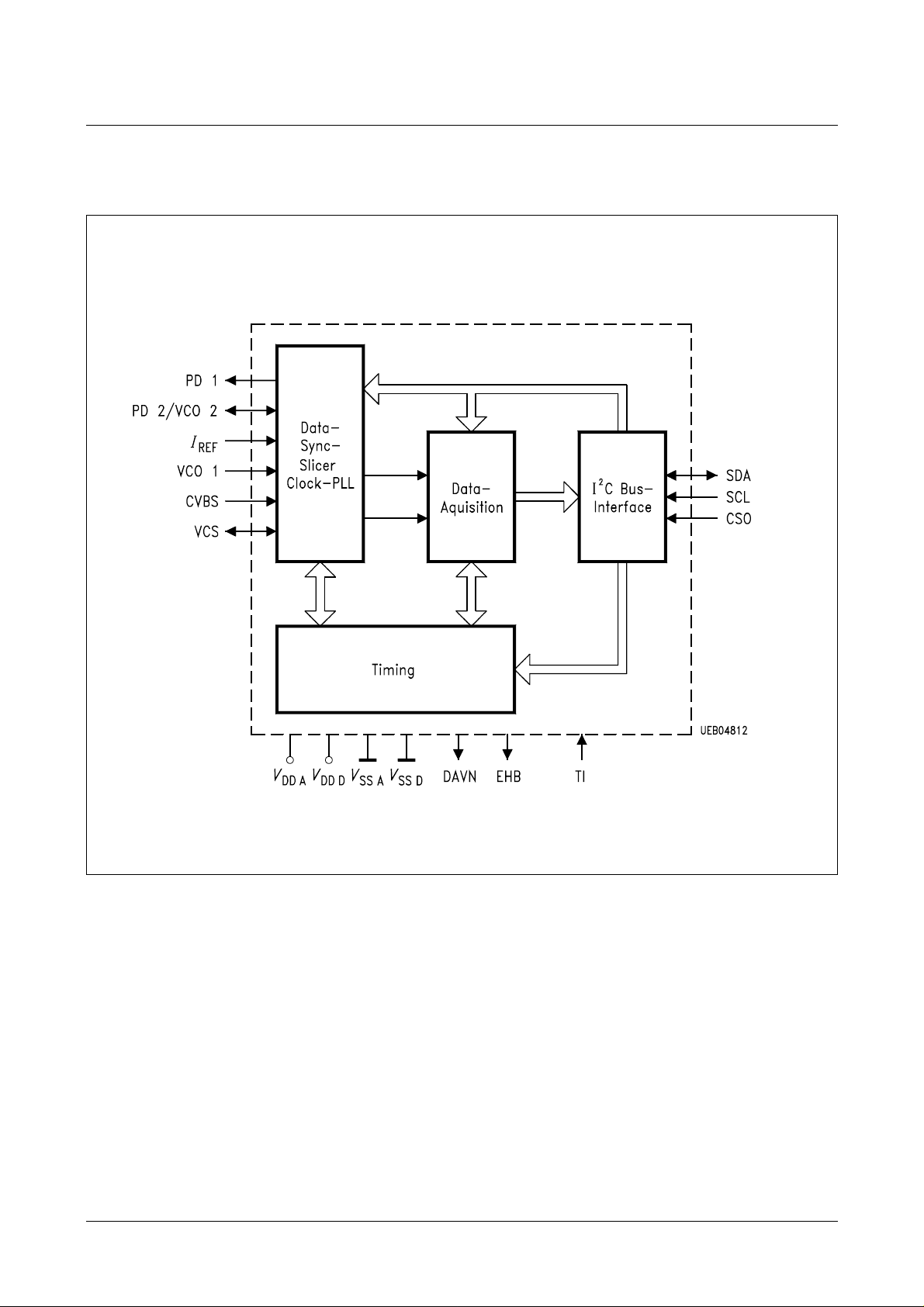
SDA 5650/X Preliminary Data Sheet
Block Diagram
Figure 2
Micronas 5
Page 8

SDA 5650/X Preliminary Data Sheet
2 System Description
2.1 Functions
Referring to the functional block diagramof the PDC/ VPS decoder,the composite video
signal with negative going sync pulses is coupled to the pin CVBS through a capacitor
which is used forclamping thebottom of the sync pulses to an internally fixed level. The
signal is passed on to the slicer, an analogue circuitry separating the sync and the data
parts of the CVBS signal, thus yielding the digital composite sync signal VCS and a
digital data signal for further processing by comparing those signals to internally
generated slicing levels.
The output of the sync separator is forwarded, on one hand, to the output pin VCS, and
on the other hand, to the clock generator and the timing block. The VCS signal
represents a keysignal thatis used for derivinga system clocksignal bymeans of a PLL
and all other timing signal.
The data slicer separates the data signal from the CVBS signal by comparing the video
voltage to an internally generated slicing level which is found by averaging the data
signal during TV line no. 16 in the VPS mode or by averaging the data signal during the
clock run-in period of the teletext lines during the data entry window (DEW) in PDC
mode.
The clock generator delivers the system clock needed for the basic timing as well as for
the regeneratonof the dataclock. It is based on two phase locked loops (PLL’s) all parts
of which are integrated on chip with the exception of the loop filter components. Each of
the PLL’s is composed of a voltage controlled relaxation oscillator (VCO), a phase/
frequency detector (PFD), and a charge pump which converts the digital output signals
of the PFD to an analogue current. That current is transformed to a control voltage for
the VCO by the off-chip loop filter. The generated VCO frequencies are 10 MHz and
13.875 MHz for VPS mode and PDC mode, respectively.
All signals necessary for the control of sync and data slicing as well as for the data
acquisition are generated by the Timing block.
The SDA 5650 can be operated in three different modes: Depending on the selected
operating mode, either teletext lines carrying 8/30 packages, the dedicated TV line
no. 16 (VPS) or the teletext header bytes 38-45, 30-37, 22-29 and 14-21 are acquired.
In PDC mode, only teletext rows 8/30 containing Broadcast Data Service Package
(BDSP) information are acquired. The relevant bytes of 8/30 format 1 (8/30/1) and 8/30
format 2 (8/30/2) are extracted. The 8/30/1-bytes are stored in the acquisition register in
a transparent way without any bit manipulation, whereas the Hamming coded bytes of
packet 8/30/2 are Hamming-checked and bytes with one bit error are corrected. The
storage of error free or corrected 8/30/2-data bytesin the transferregister to the I
2
C Bus
is signalled by the DAVN output going low.
Micronas 6
Page 9

SDA 5650/X Preliminary Data Sheet
In VPS mode, the extracted data bits of TV line no. 16 are checked for biphase errors.
With no biphase errors encountered, the acquired bytes are stored in the transfer
register to the I
as well.
In TTX header mode A bytes 38-45 and 30-37 are accessed in this order. This assures
software compatibility to the SDA 5649. In mode B bytes 22-29 and 14-21 are accessed
in this order.
In all three operating modes data are updated when a new data line has been received,
provided that the chip is not accessed via the I2C Bus at the same time.
A micro controller can read the stored bytes via the I
However, one must beaware that the storage of new data from the acquisition interface
is inhibited as long as the PDC decoder is being accessed via the I
Note: In order to achieve maximum system performance it is recommended to start the
SDA 5650 in VPS mode (state after power on) and read the register to check
whether line 16 is received. After reception of VPS data inline 16 the SDA 5650
can be switched to 8/30 mode and waiting for packet 8/30 data. Since VPS data
in line 16 is transmitted every frame and PDC data in packet 8/30 is transmitted
nearly every second the recognition of both VPS and 8/30 packets can be done
within PDC-system constraints (about 1 sec).
2
C Bus. That transfer is signalled by a H/L transition of the DAVN output,
2
C-Bus interface at any time.
2
C Bus.
2.2 I
2
C Bus
2.2.1 General Information
2
The I
C-Bus interface implemented on the PDC decoder is a slave transmitter/receiver,
i. e., both reading from and writing to the PDC / VPS decoder is possible. The clock line
SCL is controlled only by the bus master usually being a micro controller, whereas the
SDA line is controlled either by the master or by the slave. A data transfer can only be
initiated by the bus master when the bus is free, i. e., both SDA and SCL lines are in a
high state. As a general rule for the I
2
C Bus, the SDA line changes state only when the
SCL line is low. The only exception to that rule are the Start Condition and the Stop
Condition. Further Details are given below. The following abbreviations are used:
START: Start Condition generated by master
AS: Acknowledge by slave
AM: Acknowledge by master
NAM: No Acknowledge by master
STOP: Stop condition generated by master
Micronas 7
Page 10
SDA 5650/X Preliminary Data Sheet
2.2.2 Chip Address
There are two pairs of chip addresses, which are selected by the CS0-input pin
according to the following table:
CS0 Input Write Mode Read Mode
Low 20 (hex) 21 (hex)
High 22 (hex) 23 (hex)
2.2.3 Write Mode
For writing to the PDC decoder, the following format has to be used:
Start Chipaddress and Write Mode AS Byte to set Control Register AS Stop
Description of Data Transfer (Write Mode)
Step1: In order to starta data transfer the master generates a Start Condition on the
bus by pulling the SDA line low while the SCL line is held high.
Step 2: The bus master puts the chip address on the SDA line during the next eight
SCL pulses.
Step 3: The master releases theSDA lineduring theninth clockpulse. Thus the slave
can generate an acknowledge (AS) by pulling the SDA line to a low level.
Step 4: The controller transmits the data byte to set the Control register
Step 5: The slave acknowledges the reception of the byte.
Step 6: The master concludes the data communication by generating a Stop
Condition.
2
The write mode is used to set the I
C-Bus control register which determines the
operating mode:
Micronas 8
Page 11

SDA 5650/X Preliminary Data Sheet
Control Register:
Bit Number: 76543210
T4 T3 T2 T1 MAB HDT PDC/
VPS
FOR1/
FOR2
Default: All bits are set to 0 on power-up.
Bits 4 through 7 are used for test purposes and must not be changed for normal
operation by user software!
2
Bit 0: determines, which kindof data isaccessed via theI
C Bus whenPDC
mode is active:
Value
01
BDSP 8/ 30/ 2 data accessible BDSP 8/ 30/ 1 or header row
data accessible (refer to description of
Bit 2)
Bit 1: determines the operating mode:
Value
01
VPS mode active PDC mode active
Bit 2: determines whether BDSP 8/30/1-data or header row data is
accessible:
Value
01
BDSP 8/30/1 data accessible Bytes of teletext header in mode A or B
(see Bit 3)
Bit 3: determines mode of teletext header access:
Value
01
Mode A: header bytes in order 38-45,
30-37
Mode B: header bytes in order 22-29,
14-21
Micronas 9
Page 12

SDA 5650/X Preliminary Data Sheet
2.2.4 Read Mode
For reading from the PDC decoder, the following format has to be used
Start Chipaddress Read Mode AS 1stByte AM ..... Last Byte NAM Stop
The contents of up to 16 registers (bytes) can be read starting with byte 1 bit 7 (refer to
the table Order of Data Output on the I
operating mode.
Description of Data Transfer (Read Mode)
Step1: To start a data transfer the master generates a Start Condition on the bus by
pulling the SDA line low while the SCL line is held high. The byte address
counter in the decoder is reset and points to the first byte to be output.
Step 2: The bus master puts the chip address on the SDA line during the next eight
SCL pulses.
2
C Bus and...) depending on the selected
Step 3: The master releases theSDA lineduring theninth clockpulse. Thus the slave
can generate an acknowledge (AS) by pulling the SDA line to a low level. At
this moment, the slave switches to transmitting mode.
Step 4: During the next eight clock pulses the slave puts the addressed data byte
onto the SDA line.
Step 5: The reception of the byte is acknowledged by the master device which, in
turn, pulls down the SDA line during the next SCL clock pulse. By
acknowledging a byte, the master prompts the slave to increment its internal
address counter and to provide the output of the next data byte.
Step 6: Steps no. 4 and no. 5 are repeated, until the desired amount of bytes have
been read.
Step 7: The last byte is output by the slave since it will not be acknowledged by the
master.
Step 8: To conclude the read operation, the masterdoesn’t acknowledge thelast byte
to be received. A No Acknowledge by the master (NAM) causes the slave to
switch from transmitting to receiving mode. Note that the master can
prematurely cease any reading operation by not acknowledging a byte.
Step 9: The master gains control over the SDA line and concludes the data transfer
by generating a Stop Condition on the bus, i. e., by producing a low/high
transition on the SDA line while the SCL line is in a high state. With the SDA
2
and the SCL lines being both ina high state, the I
C Bus is free and ready for
another data transfer to be started.
Micronas 10
Page 13
SDA 5650/X Preliminary Data Sheet
2.3 Order of Data Output on the I2C Bus and Bit Allocation of PDC/VPS
Operating Modes
2
I
C Bus PDC Packet 8/30 VPS Mode
Format 1 Format 2
Byte 1 bit 7
t
byte 15 bit 0
6
5
4
3
2
1
0
2)
byte 16 bit 0
1
2
3
4
byte 17 bit 0
5
6
7
1)
byte 11 bit 0
1
2
3
2)
1
2
3
4
1
2
3
5
6
7
Byte 2 bit 7
Byte 3 bit 7
Byte 4 bit 7
byte 16 bit 0
6
5
4
3
2
1
0
1
2
3
4
5
6
7
byte 17 bit 0
6
5
4
3
2
1
0
1
2
3
4
5
6
7
byte 18 bit 0
6
5
4
3
2
1
0
1
2
3
4
5
6
7
byte 18 bit 0
1
2
3
byte 19 bit 0
1
2
3
byte 20 bit 0
1
2
3
byte 21 bit 0
1
2
3
byte 22 bit 0
1
2
3
byte 23 bit 0
1
2
3
byte 12 bit 0
1
2
3
4
5
6
7
byte 13 bit 0
1
2
3
4
5
6
7
byte 14 bit 0
1
2
3
4
5
6
7
1)
Message bit numbers according to EBU specification of PDC system.
2)
Transmission bit number.
Micronas 11
Page 14

SDA 5650/X Preliminary Data Sheet
2.3 Order of Data Output on the I2C Bus and Bit Allocation of PDC/VPS
Operating Modes (cont’d)
2
I
C Bus PDC Packet 8/30 VPS Mode
Format 1 Format 2
Byte 5 bit 7
Byte 6 bit 7
Byte 7 bit 7
byte 19 bit 0
6
5
4
3
2
1
0
1
2
3
4
5
6
7
byte 20 bit 0
6
5
4
3
2
1
0
1
2
3
4
5
6
7
byte 21 bit 0
6
5
4
3
2
1
0
1
2
3
4
5
6
7
byte 14 bit 0
1
2
3
byte 15 bit 0
1
2
3
byte 24 bit 0
1
2
3
byte 25 bit 0
1
2
3
byte 13 bit 0
1
2
3
– set to “1”
– set to “1”
– set to “1”
– set to “1”
byte 5 bit 0
1
2
3
4
5
6
7
byte 15 bit 0
1
2
3
4
5
6
7
– set to “1”
– set to “1”
– set to “1”
– set to “1”
– set to “1”
– set to “1”
– set to “1”
– set to “1”
Byte 8 bit 7
6
5
4
3
2
1
0
1)
Message bit numbers according to EBU specification of PDC system.
2)
Transmission bit number.
Micronas 12
byte 13 bit 0
1
2
3
4
5
6
7
Page 15

SDA 5650/X Preliminary Data Sheet
2.3 Order of Data Output on the I2C Bus and Bit Allocation of PDC/VPS
Operating Modes (cont’d)
2
I
C Bus PDC Packet 8/30 VPS Mode
Format 1 Format 2
Byte 9 bit 7
Byte 10 bit 7
Byte 11 bit 7
byte 14 bit 0
6
5
4
3
2
1
0
1
2
3
4
5
6
7
byte 22 bit 0
6
5
4
3
2
1
0
1
2
3
4
5
6
7
byte 23 bit 0
6
5
4
3
2
1
0
1
2
3
4
5
6
7
1)
Message bit numbers according to EBU specification of PDC system.
2)
Transmission bit number.
Micronas 13
Page 16

SDA 5650/X Preliminary Data Sheet
2.3 Order of Data Output on the I2C Bus and Bit Allocation of PDC/VPS
Operating Modes (cont’d)
2
I
C Bus PDC Packet 8/30 VPS Mode
Format 1 Format 2
Byte 12 bit 7
6
5
4
3
2
1
0
Byte 13 bit7
6
5
4
3
2
1
0
1)
Message bit numbers according to EBU specification of PDC system.
2)
Transmission bit number.
byte 24 bit 0
1
2
3
4
5
6
7
byte 25 bit 0
1
2
3
4
5
6
7
Micronas 14
Page 17

SDA 5650/X Preliminary Data Sheet
2.4 Order of Data Output on the I2C Bus and Bit Allocation for the Header
Time Mode (MAB = 0)
2
I
C Bus Header Time Mode
t
Byte 1 bit 7
byte 38 bit 0
6
5
4
3
2
1
0
2)
1
2
3
4
5
6
7
Byte 2 bit 7
Byte 3 bit 7
Byte 4 bit 7
byte 39 bit 0
6
5
4
3
2
1
0
1
2
3
4
5
6
7
byte 40 bit 0
6
5
4
3
2
1
0
1
2
3
4
5
6
7
byte 41 bit 0
6
5
4
3
2
1
0
1
2
3
4
5
6
7
1)
Message bit numbers according to EBU specification of PDC system.
2)
Transmission bit number.
Micronas 15
Page 18

SDA 5650/X Preliminary Data Sheet
2.4 Order of Data Output on the I2C Bus and Bit Allocation for the Header
Time Mode (MAB = 0) (cont’d)
2
I
C Bus Header Time Mode
t
Byte 5 bit 7
byte 42 bit 0
6
5
4
3
2
1
0
2)
1
2
3
4
5
6
7
Byte 6 bit 7
Byte 7 bit 7
Byte 8 bit 7
byte 43 bit 0
6
5
4
3
2
1
0
1
2
3
4
5
6
7
byte 44 bit 0
6
5
4
3
2
1
0
1
2
3
4
5
6
7
byte 45 bit 0
6
5
4
3
2
1
0
1
2
3
4
5
6
7
1)
Message bit numbers according to EBU specification of PDC system.
2)
Transmission bit number.
Micronas 16
Page 19

SDA 5650/X Preliminary Data Sheet
2.4 Order of Data Output on the I2C Bus and Bit Allocation for the Header
Time Mode (MAB = 0) (cont’d)
2
I
C Bus Header Time Mode
t
Byte 9 bit 7
byte 30 bit 0
6
5
4
3
2
1
0
2)
1
2
3
4
5
6
7
Byte 10 bit 7
Byte 11 bit 7
Byte 12 bit 7
byte 31 bit 0
6
5
4
3
2
1
0
1
2
3
4
5
6
7
byte 32 bit 0
6
5
4
3
2
1
0
1
2
3
4
5
6
7
byte 33 bit 0
6
5
4
3
2
1
0
1
2
3
4
5
6
7
1)
Message bit numbers according to EBU specification of PDC system.
2)
Transmission bit number.
Micronas 17
Page 20

SDA 5650/X Preliminary Data Sheet
2.4 Order of Data Output on the I2C Bus and Bit Allocation for the Header
Time Mode (MAB = 0) (cont’d)
2
I
C Bus Header Time Mode
t
Byte 13 bit 7
byte 34 bit 0
6
5
4
3
2
1
0
2)
1
2
3
4
5
6
7
Byte 14 bit 7
Byte 15 bit 7
Byte 16 bit 7
byte 35 bit 0
6
5
4
3
2
1
0
1
2
3
4
5
6
7
byte 36 bit 0
6
5
4
3
2
1
0
1
2
3
4
5
6
7
byte 37 bit 0
6
5
4
3
2
1
0
1
2
3
4
5
6
7
1)
Message bit numbers according to EBU specification of PDC system.
2)
Transmission bit number.
Micronas 18
Page 21

SDA 5650/X Preliminary Data Sheet
2.4 Order of Data Output on the I2C Bus and Bit Allocation for the Header
Time Mode (MAB = 0) (cont’d)
2
I
C Bus Header Time Mode
t
Byte 1 bit 7
byte 22 bit 0
6
5
4
3
2
1
0
2)
1
2
3
4
5
6
7
Byte 2 bit 7
Byte 3 bit 7
Byte 4 bit 7
byte 23 bit 0
6
5
4
3
2
1
0
1
2
3
4
5
6
7
byte 24 bit 0
6
5
4
3
2
1
0
1
2
3
4
5
6
7
byte 25 bit 0
6
5
4
3
2
1
0
1
2
3
4
5
6
7
1)
Message bit numbers according to EBU specification of PDC system.
2)
Transmission bit number.
Micronas 19
Page 22

SDA 5650/X Preliminary Data Sheet
2.4 Order of Data Output on the I2C Bus and Bit Allocation for the Header
Time Mode (MAB = 0) (cont’d)
2
I
C Bus Header Time Mode
t
Byte 5 bit 7
byte 26 bit 0
6
5
4
3
2
1
0
2)
1
2
3
4
5
6
7
Byte 6 bit 7
Byte 7 bit 7
Byte 8 bit 7
byte 27 bit 0
6
5
4
3
2
1
0
1
2
3
4
5
6
7
byte 28 bit 0
6
5
4
3
2
1
0
1
2
3
4
5
6
7
byte 29 bit 0
6
5
4
3
2
1
0
1
2
3
4
5
6
7
1)
Message bit numbers according to EBU specification of PDC system.
2)
Transmission bit number.
Micronas 20
Page 23

SDA 5650/X Preliminary Data Sheet
2.4 Order of Data Output on the I2C Bus and Bit Allocation for the Header
Time Mode (MAB = 0) (cont’d)
2
I
C Bus Header Time Mode
t
Byte 9 bit 7
byte 14 bit 0
6
5
4
3
2
1
0
2)
1
2
3
4
5
6
7
Byte 10 bit 7
Byte 11 bit 7
Byte 12 bit 7
byte 15 bit 0
6
5
4
3
2
1
0
1
2
3
4
5
6
7
byte 16 bit 0
6
5
4
3
2
1
0
1
2
3
4
5
6
7
byte 17 bit 0
6
5
4
3
2
1
0
1
2
3
4
5
6
7
1)
Message bit numbers according to EBU specification of PDC system.
2)
Transmission bit number.
Micronas 21
Page 24

SDA 5650/X Preliminary Data Sheet
2.4 Order of Data Output on the I2C Bus and Bit Allocation for the Header
Time Mode (MAB = 0) (cont’d)
2
I
C Bus Header Time Mode
t
Byte 13 bit 7
byte 18 bit 0
6
5
4
3
2
1
0
2)
1
2
3
4
5
6
7
Byte 14 bit 7
Byte 15 bit 7
Byte 16 bit 7
byte 19 bit 0
6
5
4
3
2
1
0
1
2
3
4
5
6
7
byte 20 bit 0
6
5
4
3
2
1
0
1
2
3
4
5
6
7
byte 21 bit 0
6
5
4
3
2
1
0
1
2
3
4
5
6
7
1)
Message bit numbers according to EBU specification of PDC system.
2)
Transmission bit number.
Micronas 22
Page 25

SDA 5650/X Preliminary Data Sheet
2.5 Description of DAVN and EHB Outputs
DAVN (Data Valid active low)
EHB (First Field active high)
Signal Output VPS Mode PDC Mode
8/30/2 Mode 8/30/1 Mode Header Time
DAVN
H/L-transition
(set low)
in line 16 when
validVPS datais
received
in the line
carrying
valid
8/30/2 data
in the line
carrying
valid
8/30/1 data
in the line
carrying
valid
header
row X/0 data
L/H-transition
(set high)
always set high on power-up or during I
at the start of
line 16
at the beginning of the next field
i.e., at the start of the next data entry window
2
C-Bus accesses when the bus master
doesn’t acknowledge in order to generate the stop condition
EHB
L/H-transition at the beginning of the first field
H/L-transition at the beginning of the second field
In test mode (i.e. TI = high), both DAVN and EHB are controlled by the CS0 pin and
reproduce the state of the CS0 input.
Micronas 23
Page 26

SDA 5650/X Preliminary Data Sheet
3 Electrical Characteristics
Absolute Maximum Ratings
T
= 25 °C
A
Parameter Symbol Limit Values Unit Test
min. typ. max.
Condition
Ambient temperature
Storage temperature
Total power dissipation
Power dissipation per
T
T
P
P
A
stg
tot
DQ
070°C in operation
–40 125 °C by storage
300 mW
10 mW
output
Input voltage
Supply voltage
Thermal resistance
V
V
R
IM
DD
th SU
– 0.3 6 V
– 0.3 6 V
80 K/W
Note: Maximum ratings are absolute ratings; exceeding any one of these values may
cause irreversible damage to the integrated circuit.
Operating Range
Supply voltage
Supply current
V
I
DD
DD
4.5 5 5.5 V
515mA
Ambient temperature
T
A
070°C
range
Note: In the operating range the functions given in the circuit description are fulfilled.
Micronas 24
Page 27

SDA 5650/X Preliminary Data Sheet
Electrical Characteristics
T
= 25 °C
A
Parameter Symbol Limit Values Unit Test Condition
min. typ. max.
Input Signals SDA, SCL, CS0
H-input voltage
L-input voltage
Input capacitance
Input current
V
V
C
I
Input Signal TI
H-input voltage V
L-input voltage
Input capacitance
Input current
V
C
I
Input Signals CVBS
(pos. Video, neg. Sync)
Video input signal
V
level
IH
IL
I
IM
IH
IL
I
IM
CVBS
0.7 × V
DD
V
DD
V
0 0.3 × VDDV
10 pF
10 µA
0.9 × V
DD
V
DD
V
0 0.1 × VDDV
10 pF
10 µA
0.7 1.0 2.0 V 2 Vpp with
0.8 V
1.2 V
V
SYNC
V
DAT
and
Synchron signal
V
SYNC
0.15 0.3 0.8 (1.0) V 1.0 V only
amplitude
Data amplitude
Coupling capacitor
H-input current
L-input current
Source impedance
Leakage resistance
V
C
I
I
R
R
DAT
C
IH
IL
S
C
0.25
1.5 ×
V
SYNC
– 1000 – 400 – 100 µA VI=0V
0.91 1 1.2 MΩ
at coupling capacitor
Micronas 25
related to VCS
signal generation
0.5 1.2 V
33 nF
10 µA VI=5V
250 Ω
Page 28

SDA 5650/X Preliminary Data Sheet
Electrical Characteristics (cont’d)
T
= 25 °C
A
Parameter Symbol Limit Values Unit Test Condition
min. typ. max.
Output Signals DAVN, EHB, VCS
H-output voltage
L-output voltage
V
V
QH
QL
V
– 0.5 V IQ= – 100 µA
DD
0.4 V IQ= 1.6 mA
Output Signals SDA (Open-Drain-Stage)
L-output voltage V
Permissible output
QL
0.4 V IQ= 3.0 mA
5.5 V
voltage
PLL-Loop Filter Components (see application circuit)
Resistance at PD2/
R
1
6.8 kΩ
VCO2
Resistance at VCO1
Attenuation
R
R
2
3
1200 kΩ
6.8 kΩ
resistance
Resistance at PD2/
R
5
1200 kΩ
VCO2
Integration capacitor
Integration capacitor
C
C
1
3
2.2 nF
33 nF
VCO – Frequence Range Adjustment
Resistance at IREF
R
4
100 kΩ
(for bias current
adjustment)
Note:The listed characteristics are ensured over the operating range of the integrated
circuit. Typical characteristics specify mean values expected over the production
spread. If not otherwise specified, typical characteristics apply at
T
=25°C and
A
the given supply voltage.
Micronas 26
Page 29

SDA 5650/X Preliminary Data Sheet
t
HD, STA
SDA
SCL
t
t
BUF
Stop Start Stop
t
LOW
TLH
t
HD, DAT SU, DAT
t
THL
t
HIGH
t t
SU, STO
UET00130
Figure 3
2
I
C-Bus Timing
Parameter Symbol Limit Values Unit
min. max.
Clock frequency f
Inactive time prior to new transmission start-up
SCL
t
BUF
0 100 kHz
4.7 µs
Hold time during start condition
Low-period of clock
High-period of clock
Set-up time for data
Rise time for SDA and SCL signal
Fall time for SDA and SCL signal
Set-up time for SCL clock during stop condition
V
All values referred to
and VIL levels.
IH
t
HD; STA
t
LOW
t
HIGH
t
SU;DAT
t
TLH
t
THL
t
SU; STO
4.0 µs
4.7 µs
4.0 µs
250 ns
1 µs
300 ns
4.7 µs
Micronas 27
Page 30

SDA 5650/X Preliminary Data Sheet
4 PDC/VPS-Receiver
Figure 4
Micronas 28
Page 31

SDA 5650/X Preliminary Data Sheet
5 Appendix
2
5.1 Control Register Write (I
C-Bus Write)
Figure 5
5.2 Data Register Read (I
2
C-Bus Read)
Figure 6
Micronas 29
Page 32

SDA 5650/X Preliminary Data Sheet
5.3 DAVN and EHB Timing
Figure 7
Micronas 30
Page 33

SDA 5650/X Preliminary Data Sheet
5.4 Position of Teletext and VPS Data Lines within the Vertical Blanking
Interval
Figure 8
5.5 Definition of Voltage Levels for VPS Data Line
Figure 9
Micronas 31
Page 34

SDA 5650/X Preliminary Data Sheet
5.6 BDSP 8/30 Format 1 Bit Allocation
ByteNo. Bit No. Contents
01234567
13 Network Identification 1. Byte
14 Network Identification 2. Byte
15 Weight Weight Sign Time Offset Code
–22–120
2
1
2
2
2
3
2
0
1
16 MJD Digit
Weight 10
17 MJD Digit
Weight 10
18 MJD Digit
Weight 10
19 UTC Hours
Units
4
2
0
1 1 1 1 Modified Julian Date (MJD)
1. Byte
MJD Digit
Weight 10
MJD Digit
Weight 10
UTC Hours
Tens
3
1
Modified Julian Date
2. Byte
Modified Julian Date (MJD)
3. Byte
Universal Time Coordinated
(UTC)
1. Byte
20 UTC Minutes
Units
21 UTC Seconds
Units
UTC Minutes
Tens
UTC Seconds
Tens
Universal Time Coordinated
2. Byte
Universal Time Coordinated
3. Byte
22 Short Programme Label 1. Byte
23 Short Programme Label 2. Byte
24 Short Programme Label 3. Byte
25 Short Programme Label 4. Byte
Note: This corresponds to the coding adopted in CCIR teletext system B BDSP 8/30
format 1.
NB: The received bytes are output on the I
2
C Bus in a transparent way, i.e., on a
bit-first-in-first-out basis. No bit manipulation is performed on the chip in this
operating mode.
Concerning bytes no. 16 through 21: When evaluating the numbers, note that
each 4-bit-digit has been incremented by one prior to transmission, and the least
significant bits are transmitted first.
Micronas 32
Page 35

SDA 5650/X Preliminary Data Sheet
5.7 Structure of the Teletext Data Packet 8/30 Format 2
Figure 10
:
5.8 BDSP 8/30 Format 2 Bit Allocation
The four message bits of byte 13 are used as follows
byte 13 bit 0 – LCI b
1 – LCI b
1
2
label channel identifier
2 – LUF label update flag
3 – reserved
but as yet
undefined
Micronas 33
Page 36

SDA 5650/X Preliminary Data Sheet
5.8 BDSP 8/30 Format 2 Bit Allocation (cont’d)
The message bits of bytes 14-25 are used in a way similar to the coding of the label in
the dedicated television line as follows:
byte 14 bit 0 PCS b
1 PCS b
2 reserved but yet
3 undefined
byte 15 bit 0 CNI b
1 CNI b
2 CNI b
3 CNI b
byte 16 bit 0 CNI b
1 CNI b
2 PIL b
3 PIL b
byte 17 bit 0 PIL b
1 PIL b
2 PIL b
1
2
1
2
3
4
9
10
1
2
3
4
5
status of analogue sound
country
network (or programme provider)
day
3 PIL b
byte 18 bit 0 PIL b
1 PIL b
2 PIL b
3 PIL b
byte 19 bit 0 PIL b
1 PIL b
2 PIL b
3 PIL b
6
7
8
9
10
11
12
13
14
month
hour
Micronas 34
Page 37

SDA 5650/X Preliminary Data Sheet
5.8 BDSP 8/30 Format 2 Bit Allocation (cont’d)
byte 20 bit 0 PIL b
1 PIL b
2 PIL b
3 PIL b
byte 21 bit 0 PIL b
1 PIL b
2 CNI b
3 CNI b
byte 22 bit 0 CNI b
1 CNI b
2 CNI b
3 CNI b
byte 23 bit 0 CNI b
1 CNI b
2 CNI b
15
16
17
18
19
20
5
6
7
8
11
12
13
14
15
minute
country
network (or programme provider)
3 CNI b
byte 24 bit 0 PTY b
1 PTY b
2 PTY b
3 PTY b
byte 25 bit 0 PTY b
1 PTY b
2 PTY b
3 PTY b
16
1
2
3
4
5
6
7
8
programme type
Micronas 35
Page 38

SDA 5650/X Preliminary Data Sheet
5.9 Data Format of Programme Delivery Data in the Dedicated TV Line (VPS)
Figure 11
Micronas 36
Page 39

SDA 5650/X Preliminary Data Sheet
Figure 12
Micronas 37
Page 40

SDA 5650/X Preliminary Data Sheet
6 Package Outlines
P-DIP-14-1
(Plastic Dual In-line Package)
Sorts of Packing
Package outlines for tubes, trays etc. are contained in our
Data Book “Package Information”.
GPD05005
Dimensions in mm
Micronas 38
Page 41

SDA 5650/X Preliminary Data Sheet
P-DSO-20-1
(Plastic Dual Small Outline Package)
0.35 x 45˚
7.6
10.3
-0.2
0.4
±0.3
GPS05094
1)
+0.8
+0.09
0.23
8˚ max
0.35
1.27
+0.15
-0.2
-0.1
0.2
2.45
2.65 max
2)
0.2 24x
0.1
1120
110
12.8
-0.2
1)
Index Marking
1) Does not include plastic or metal protrusions of 0.15 max per side
2) Does not include dambar protrusion of 0.05 max per side
GPS05094
Sorts of Packing
Package outlines for tubes, trays etc. are contained in our
Data Book “Package Information”.
SMD = Surface Mounted Device
Micronas 39
Dimensions in mm
Page 42

SDA 5650/X PRELIMINARY DATA SHEET
Micronas GmbH
Hans-Bunte-Strasse 19
D-79108 Freiburg (Germany)
P.O. Box 840
D-79008 Freiburg (Germany)
Tel. +49-761-517-0
Fax +49-761-517-2174
E-mail: docservice@micronas.com
Internet: www.micronas.com
Printed in Germany
Order No. 6251-563-1PD
All information and data contained in this data sheet are without any
commitment, are not to be considered as an offer for conclusion of a
contract, nor shall they be construed as to create any liability. Any new
issue of this data sheet invalidates previous issues. Product availability
and delivery ar e exclusively subj ec t t o o ur re s pe ct ive or der co nf irm at ion
form; the same applies to orders based on development samples delivered. By this pu bli cat io n, Mi cr on as Gmb H do es no t assu m e r es po n sibi lity for patent infringements or other ri ghts of third parties which m ay
result from its use.
Further , M icro nas G mbH r eserv es th e righ t to revis e thi s pu blicat ion a nd
to make chang es to its cont en t, at any time , wi thout obli gati on t o no tify
any person or entity of such revisions or changes.
No part of this publication may be reproduced, photocopied, stored on a
retrieval system, or transmitted without the express written consent of
Micronas GmbH .
40 Micronas
 Loading...