

Page 1
PLL with I2C Bus for AM/FM Receivers SDA 4331X
1 Overview
1.1 Features
• 155 MHz FM and 40 MHz AM input frequency
• 30 mVeff AM and 50 mVeff FM sensitivity
2
• Additional open drain ports controlled by I
• 2-pin quartz oscillator
• Fast phase detector with short anti-backlash pulses
and polarity reversal
• Charge pump current programmable in four steps
up to 4.5 mA
• Frequency resolution of 1, 5 and 10 kHz AM and 12.5, 25 and 50 kHz FM
• P-DSO-24 package
C Bus
P-DSO-24-1
Type Ordering Code Package
SDA 4331X Q67100-H5139 P-DSO-24-1
1.2 Application
The SDA 4331X provides separated input and output ports for AM and FM and is well
suited for extremely fast loop settling times in the FM mode.
Semiconductor Group 1 04.96
Page 2

1.3 Pin Configuration
(top view)
SDA 4331X
P-DSO-24-1
Figure 1
Semiconductor Group 2 04.96
Page 3

1.4 Pin Definitions and Functions
SDA 4331X
Pin No. Symbol Input (I)
Function
Output (O)
1 V
DD1
2 SCL I Clock I
3 SDA I/O Data I
Supply voltage digital (5 V)
2
C Bus
2
C Bus
4 A0 I Address selection, sets the LSB of the IC-address
5 N.C.
6 … 9 SA1 … SA4 O 10 V open drain output, controlled via I
2
C Bus
10 AM/FM O 10 V open drain output, indicating the operation
mode (H = AM)
11 FM
IN
12 GND
13 AM
IN
AN
I Input for the FM signal from VCO
Ground analog
I Input for the AM signal from VCO
14 N.C.
15 N.C.
16
I
REF
I Reference current, setting the base current level
for the charge pumps
17 PD
18 PD
19 PD
20 PD
21
V
DD2
FM
AM
FMA
AMA
O FM charge pump output
O AM charge pump output
O Source follower output FM
O Source follower output AM
Supply voltage digital for charge pump and source
followers (up to 10 V)
22 OSC
23 OSC
FB
IN
I/O Oscillator feedback, quartz terminal
I Oscillator input, quartz terminal, optionally input
for external reference
24 GND Ground digital
Semiconductor Group 3 04.96
Page 4
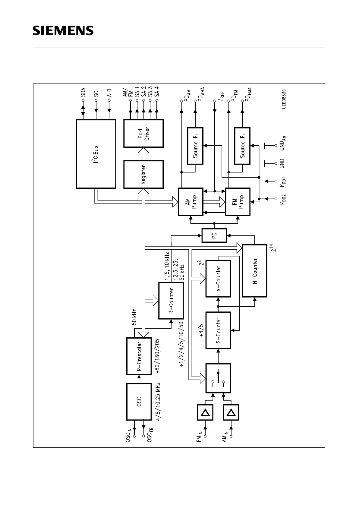
1.5 Functional Block Diagram
SDA 4331X
Figure 2
Block Diagram
Semiconductor Group 4 04.96
Page 5

SDA 4331X
2 Functional Description
2
The SDA 4331X is a radio PLL controlled via I
and FM range.
3 Circuit Description
The reference frequency for the PLL is derived from the quartz oscillator OSC
R-prescaler can be adapted to quartz frequencies of 4, 8 or 10.25 MHz, respectively,
yielding an internal 50 kHz reference. Programming the R-counter sets the phase
detector reference frequency to 1, 5 or 10 kHz in the AM mode or to 12.5, 25 or 50 kHz
in the FM mode. The VCO frequency is set by programming the A/N-counter which
operates as dual-modulus counter for FM and AM using a divide by 4/5 swallow counter.
The phase detector drives two different charge pumps for AM and FM mode. Additional
source followers are connected to the charge pump. There are four programmable
current levels for each charge pump. The supply voltage for the charge pump and the
source followers is supplied via the
V
pin and can reach 10 V maximum. AM/FM is an
DD2
open drain output as well as the additional outputs SA1 … SA4 which are controlled by
2
I
C Bus.
2
The I
selected by the A0 pin. The I
C Bus interface provides slave receiver functions. There are two addresses
2
C-protocol (see diagram 1) contains one string for
programming all counters and functions. The transfer may be stopped optionally after
each word if the remaining functions are not to be altered. After power ON all control
signals are undefined, so that the complete write sequence must be executed.
C Bus for frequency synthesis in the AM
1)
. The
1)
The power dissipation of the quartz is given by:
P
= 2 × R1 (Π×fQ× (CO + CL) × VDD)
v
R
… Series resistance of the quartz
1
f
… Quartz frequency
Q
C
… Parallel capacitance of the quartz
O
C
… Load capacitance, including input capacitance of the IC
L
2
Semiconductor Group 5 04.96
Page 6

SDA 4331X
4 Electrical Characteristics
4.1 Absolute Maximum Ratings
T
= – 25 °C to 85 °C
A
Parameter Symbol Limit Values Unit Remarks
min. max.
Supply voltage
Supply voltage
Input voltage
Power dissipation per output
Power dissipation
Storage temperature
Output voltage SA1 … SA4, AM/FM
ESD voltage (HBM: 1.5 kΩ, 100 pF)
V
V
V
P
P
T
V
V
DD1
DD2
IN
Q
tot
S
QH
ESD
– 0.3 6 V
– 0.3 10.5 V
– 0.3 V
+ 0.3 V
DD1
10 mW
t.b.d. mW
– 40 125 °C
10.5 V
– 1 1 kV
Note: Maximum ratings are absolute ratings; exceeding only one of these values may
cause irreversible damage to the integrated circuit.
4.2 Operational Range
Parameter Symbol Limit Values Unit
min. typ. max.
Supply voltage
Supply voltage
Supply current
Supply current
1)
Ambient temperature
Output voltage SA1 … SA4, AM/FM
1)
Measurement conditions: No load on pins 17 … 20.
V
V
I
I
T
V
DD1
DD2
DD1
DD2
A
QH
4.5 5 5.5 V
9 10.3 V
410mA
0.5 mA
– 25 + 85 °C
V
DD2
V
Note: In the operating range the functions given in the circuit description are fulfilled.
Semiconductor Group 6 04.96
Page 7

SDA 4331X
4.3 AC/DC Characteristics
Parameter Symbol Limit Values Unit Test Condition
min. typ. max.
Input AM
IN
Input voltage
(sine wave)
Input capacitance
Input current
Input FM
IN
Input voltage
(sine wave)
Input capacitance
Input current
Input OSC
IN
Input voltage
(sine wave)
V
C
I
V
C
I
V
IN
30 mVeff V
= 4.5 V
DD1
0.5 MHz <
f
< 40 MHz
IN
4pF
IN
IN
– 50 50 µA0≤VIN≤ V
V
= 4.5 V
DD1
50
120
mVeff
mVeff
20 MHz <
10 MHz <
DD1
f
< 120 MHz
IN
f
< 155 MHz
IN
4pF
IN
IN
– 100 100 µA0≤VIN≤ V
V
= 4.5 V
DD1
100
150
200
mVeff
mVeff
mVeff
f
= 4 MHz
IN
f
= 8 MHz
IN
f
= 10.25 MHz
IN
DD1
Input capacitance
Input current
C
I
IN
– 30 30 µA0≤V
10 pF
≤V
Q
DD1
Input/Output SDA
H-input voltage
L-input voltage
L-output voltage
Input leakage current
Input capacitance
Semiconductor Group 7 04.96
V
IH
V
IL
V
QL
I
Leakage
C
0.7 ×
V
DD1
0 0.3 ×
V
V
DD1
DD1
V
V
0.4 V IQL = 3 mA, V
C
= 400 pF
L
– 10 10 µA0≤VIN≤ V
10 pF
DD1
DD1
= 5 V,
Page 8

SDA 4331X
4.3 AC/DC Characteristics (cont’d)
Parameter Symbol Limit Values Unit Test Condition
min. typ. max.
Inputs SCL, A0
H-input voltage
L-input voltage
Input leakage current
Input capacitance
V
IH
V
IL
I
Leakage
C
0.7 ×
V
DD1
0 0.3 ×
V
V
DD1
DD1
V
V
– 10 10 µA0≤VIN≤ V
10 pF
Outputs SA1, SA2, SA3, SA4, AM/FM (open drain outputs)
L-output voltage
Input I
REF
Input current I
Voltage at
I
REF
V
V
V
QL
QL
IN
IREF
t.b.d. 100 t.b.d. µA
1.2 V IIN = 100 µA
0.4
0.1
V
V
I
= 1 mA
QL
V
= 5 V
DD1
I
= 0.1 mA
QL
DD1
Output PD
FM
PD current A I
PD current B
PD current C
PD current D
Output PD
AM
PD current A I
PD current B
PD current C
PD current D
Q
I
Q
I
Q
I
Q
Q
I
Q
I
Q
I
Q
± 4.5 mA VPD = 4 V
± 3mA
± 1.5 mA
± 150 µA
± 450 µA VPD = 4 V
± 300 µA
± 150 µA
± 30 µA
Semiconductor Group 8 04.96
Page 9

SDA 4331X
4.3 AC/DC Characteristics (cont’d)
Parameter Symbol Limit Values Unit Test Condition
min. typ. max.
Output PD
H-output voltage V
H-output current
L-output current
Output PD
H-output voltage I
L-output current
FMA
AMA
QH
I
QH
I
QL
QH
I
QL
7.5 7.7 V IQH = 2 mA
V
25mAV
10 µA V
V
1 2.5 mA V
0.1 mA V
V
PD FM
PD FM
PD FM
= 4 V
Q
PD AM
PD AM
= 5 V
Q
= V
= V
= GND
= 5 V
= GND
DD2
DD2
= 9 V
= 9 V
Note: The listed characteristics are ensured over the operating range of the integrated
circuit. Typical characteristics specify mean values expected over the production
spread. If not otherwise specified, typical characteristics apply at
T
= 25°C and
A
the given supply voltage.
Table 1
Programming of Mode and Frequency Resolution
AM/FM R1 R0 Mode Frequency Resolution [MHz]
0 0 1 FM 12.5
01 0 FM 25
01 1 FM 50
10 1 AM 1
11 0 AM 5
11 1 AM 10
Semiconductor Group 9 04.96
Page 10

SDA 4331X
Table 2
Programming R-prescaler
RP1 RP0 Divide Ratio Quartz Frequency [MHz]
0 0 1:1 Test mode only
0 1 1:80 4
1 0 1:160 8
1 1 1:205 10.25
Table 3
Programming Phase Detector
PD1 PD0 Current Level PPD Polarity
0 0 D 0 Normal
0 1 C 1 Invers
10B
11A
Table 4
Programming Test Mode
T1 T2 SA1 SA2 SA3 SA4 T3 Operation
0 0 Controlled by I
2
C Bus 0 Normal
1 0 PD_MUX Clk_50 kHz N_A_CLN 1 Test reset
Semiconductor Group 10 04.96
Page 11

Diagram 1: I2C Protocol
Slave-receive (Write)
START
1
1
0
0
1
0
0/1
0
ACK
MSB
N14
N13
N12
N11
N10
N9
N8
ACK
N7
N6
N5
N4
N3
N2
N1
LSB
ACK
[STOP or START]
AM/FM
PD1
PD0
IF
SA4
SA3
SA2
SA1
ACK
[STOP or START]
G1
G0
F0
R1
R0
RP1
RP0
0
ACK
[STOP or START]
PPD
T0 (= 0)
T1 (= 0)
T2 (= 0)
T3 (= 0)
X
X
X
ACK
STOP or START
A/N-counter
SDA 4331X
[STOP or START]:
Optional STOP or START condition, after power ON
the complete sequence has to be programmed.
Semiconductor Group 11 04.96
Page 12

SDA 4331X
Figure 3
Application Circuit for AM and FM Charge Pump Output
Semiconductor Group 12 04.96
Page 13

5 Package Outlines
P-DSO-24-1
(Plastic Dual Small Outline Package)
SDA 4331X
Sorts of Packing
Package outlines for tubes, trays etc. are contained in our
Data Book “Package Information”.
SMD = Surface Mounted Device
GPS05144
Dimensions in mm
Semiconductor Group 13 04.96
 Loading...