

Datasheet SD703C12S20L, SD703C12S30L, SD703C16S20L, SD703C16S30L, SD703C20S20L Datasheet (International Rectifier)
...Page 1

DISCRETE POWER DIODES and THYRISTORS
Next Data SheetIndex
Previous Datasheet
To Order
DATA BOOK
D-686
Page 2
Bulletin I2075/C
Next Data SheetIndex
Previous Datasheet
To Order
SD703C..L SERIES
FAST RECOVERY DIODES
Features
High power FAST recovery diode series
2.0 to 3.0 µs recovery time
High voltage ratings up to 2500V
High current capability
Optimized turn on and turn off characteristics
Low forward recovery
Fast and soft reverse recovery
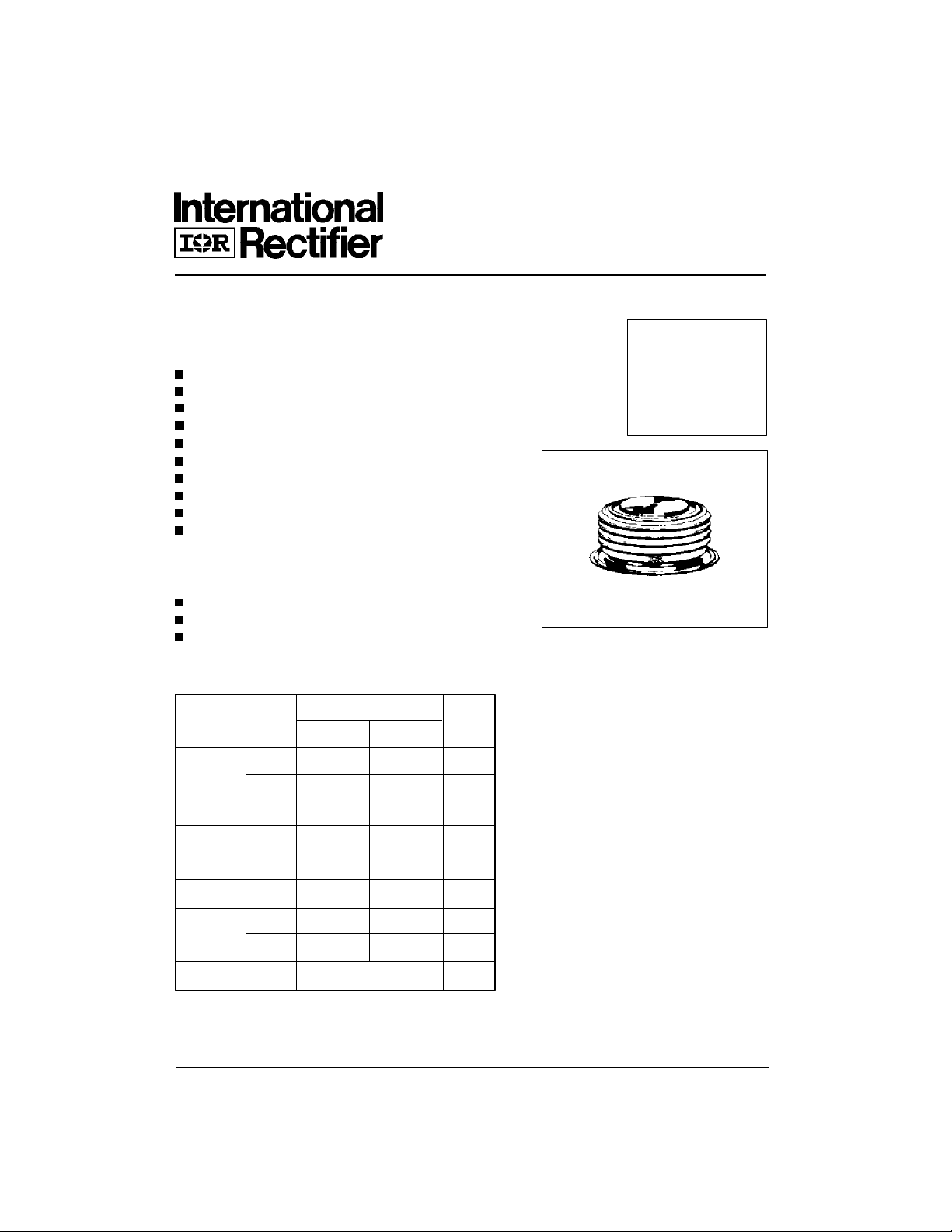
Press-puk encapsulation
Case style conform to JEDEC DO-200AB (B-PUK)
Maximum junction temperature 150°C
Typical Applications
Snubber diode for GTO
High voltage free-wheeling diode
Fast recovery rectifier applications
Major Ratings and Characteristics
Parameters Units
I
F(AV)
@ T
hs
I
F(RMS)
I
FSM
@ 50Hz 9300 9600 A
@ 60Hz 9730 10050 A
SD703C..L
S20 S30
700 790 A
55 55 °C
1320 1470 A
Hockey Puk Version
700A
790A
case style DO-200AB (B-PUK)
V
range 1200 to 2500 1200 to 2500 V
RRM
t
rr
T
J
@ T
2.0 3.0 µs
J
25 25 °C
- 40 to 150 °C
D-687
Page 3
SD703C..L Series
To Order
Next Data SheetIndex
Previous Datasheet
ELECTRICAL SPECIFICATIONS
Voltage Ratings
Voltage V
Type number Code peak reverse voltage repetitive peak rev. voltage
12 1200 1300
SD703C..L 50
16 1600 1700
20 2000 2100
25 2500 2600
Forward Conduction
Parameter Units Conditions
I
Max. average forward current 700 (365) 790 (400) A 180° conduction, half sine wave
F(AV)
@ case temperature 55 (85) 55 (85) °C Double side (single side) cooled
I
Max. RMS forward current 1320 1470 A @ 25°C heatsink temperature double side cooled
F(RMS)
I
Max. peak, one-cycle forward, 9300 9600 t = 10ms No voltage
FSM
non-repetitive surge current 9730 10050 t = 8.3ms reapplied
2
I
t Maximum I2t for fusing 432 460 t = 10ms No voltage Initial TJ = TJ max.
2
I
√t Maximum I2√t for fusing 4320 4600 KA2√s t = 0.1 to 10ms, no voltage reapplied
V
Low level value of threshold
F(TO)1
voltage
V
High level value of threshold
F(TO)2
voltage
r
Low level value of forward
1
f
slope resistance
r
High level value of forward
2
f
slope resistance
V
Max. forward voltage drop 2.20 1.85 V Ipk= 1500A, TJ = TJ max, tp = 10ms sinusoidal wave
FM
, maximum repetitive V
RRM
, maximum non- I
RSM
V V mA
SD703C..L
S20 S30
7820 8070 t = 10ms 100% V
8190 8450 t = 8.3ms reapplied Sinusoidal half wave,
395 420 t = 8.3ms reapplied
306 326 t = 10ms 100% V
279 297 t = 8.3ms reapplied
1.00 0.95 (16.7% x π x I
1.11 1.05 (I > π x I
0.80 0.60 (16.7% x π x I
0.76 0.56 (I > π x I
A
KA2s
V
mΩ
F(AV)
),TJ = TJ max.
F(AV)
F(AV)
),TJ = TJ max.
F(AV)
RRM
RRM
< I < π x I
< I < π x I
F(AV)
F(AV)
@ TJ = TJ max.
), TJ = TJ max.
), TJ = TJ max.
RRM
max.
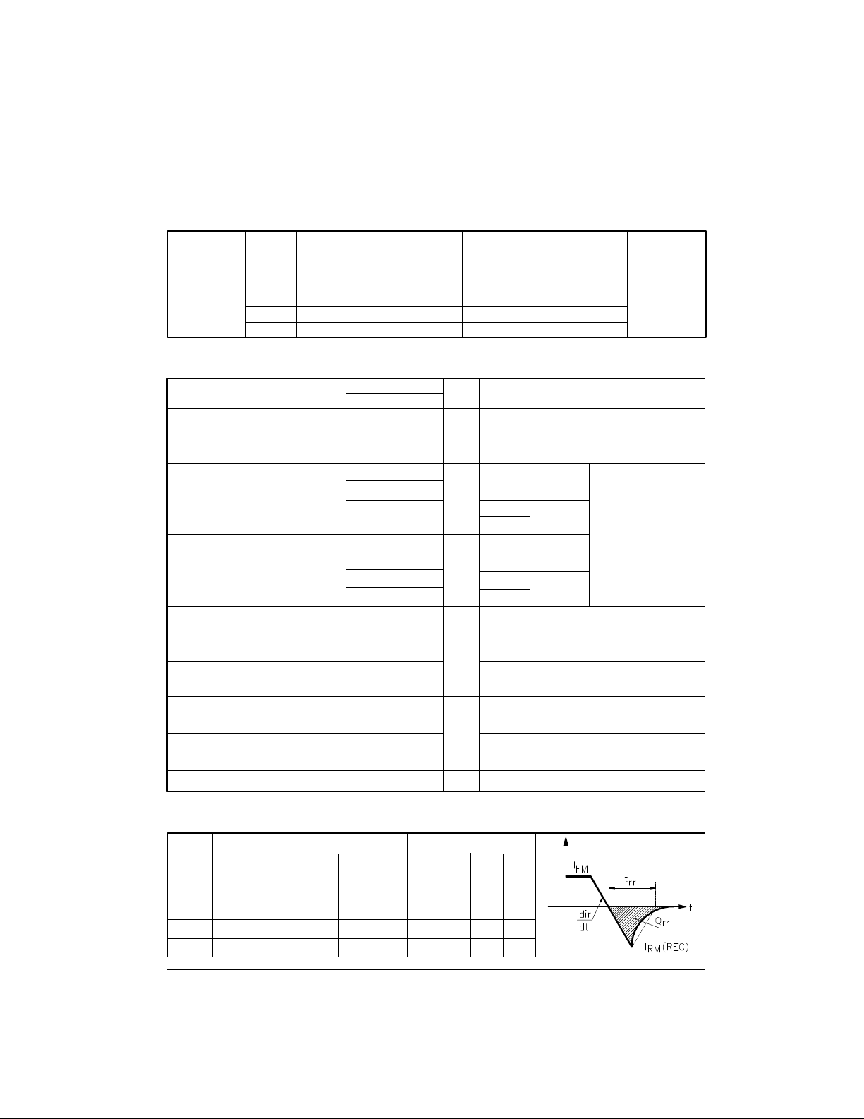
Recovery Characteristics
Code
S20 2.0 1000 50 - 50 3.5 240 110
S30 3.0 1000 50 - 50 5.0 380 130
T
= 25 oC
J
typical t
@ 25% I
rr
RRM
Test conditions Max. values @ T
I
pk
Square Pulse @ 25% I
di/dt V
r
t
rr
RRM
(µs) (A) (A/µs) (V) (µs) (µC) (A)
D-688
= 150 °C
J
QrrI
rr
Page 4
SD703C..L Series
To Order
Next Data SheetIndex
Previous Datasheet
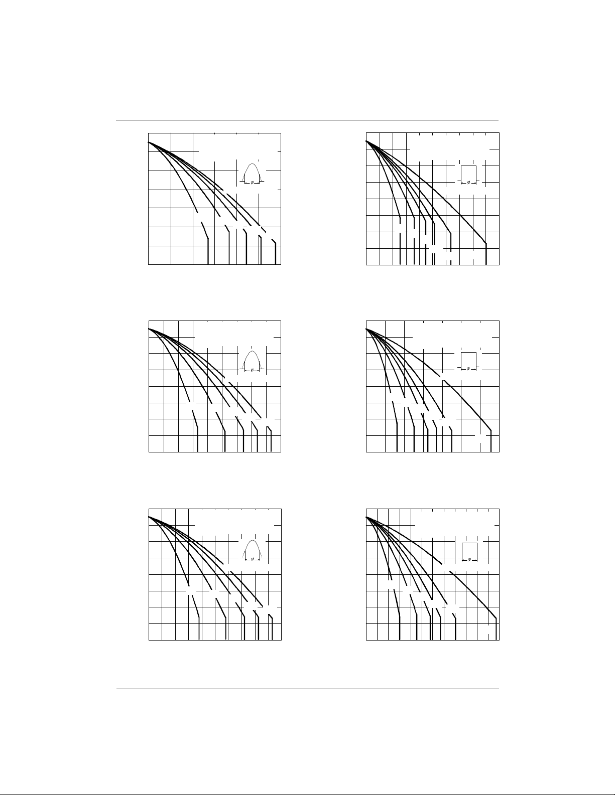
Fig. 3 - Current Ratings Characteristics Fig. 4 - Current Ratings Characteristics
Fig. 5 - Current Ratings Characteristics Fig. 6 - Current Ratings Characteristics
Fig. 7 - Current Ratings Characteristics Fig. 8 - Current Ratings Characteristics
D-691
Page 5

SD703C..L Series
To Order
Next Data SheetIndex
Previous Datasheet
Fig. 9 - Forward Power Loss Characteristics
Fig. 10 - Forward Power Loss Characteristics
Fig. 12 - Forward Power Loss CharacteristicsFig. 11 - Forward Power Loss Characteristics
Fig. 13 - Maximum Non-repetitive Surge Current
Single and Double Side Cooled
Fig. 14 - Maximum Non-repetitive Surge Current
Single and Double Side Cooled
D-692
Page 6

SD703C..L Series
To Order
Next Data SheetIndex
Previous Datasheet
Fig. 15 - Maximum Non-repetitive Surge Current
Single and Double Side Cooled
Fig. 17 - Forward Voltage Drop Characteristics
Fig. 16 - Maximum Non-repetitive Surge Current
Single and Double Side Cooled
Fig. 18 - Forward Voltage Drop Characteristics
Fig. 19 - Thermal Impedance Z
D-693
Characteristic
thJ-hs
Page 7

SD703C..L Series
To Order
Next Data SheetIndex
Previous Datasheet
Fig. 21 - Typical Forward Recovery CharacteristicsFig. 20 - Typical Forward Recovery Characteristics
Fig. 22 - Recovery Time Characteristics
Fig. 25 - Recovery Time Characteristics
Fig. 23 - Recovery Charge Characteristics
Fig. 26 - Recovery Charge Characteristics Fig. 27 - Recovery Current Characteristics
D-694
Fig. 24 - Recovery Current Characteristics
Page 8

SD703C..L Series
To Order
Next Data SheetIndex
Previous Datasheet
Fig. 28 - Maximum Total Energy Loss Per Pulse Characteristics Fig. 29 - Frequency Characteristics
Fig. 30 - Maximum Total Energy Loss Per Pulse Characteristics Fig. 31 - Frequency Characteristics
Fig. 32 - Maximum Total Energy Loss Per Pulse Characteristics Fig. 33 - Frequency Characteristics
D-695
Page 9

SD703C..L Series
To Order
Next Data SheetIndex
Previous Datasheet
Fig. 34 - Maximum Total Energy Loss Per Pulse Characteristics
Fig. 35 - Frequency Characteristics
Fig. 37 - Frequency CharacteristicsFig. 36 - Maximum Total Energy Loss Per Pulse Characteristics
Fig. 39 - Frequency CharacteristicsFig. 38 - Maximum Total Energy Loss Per Pulse Characteristics
D-696
Page 10

SD703C..L Series
To Order
Next Data SheetIndex
Previous Datasheet
Thermal and Mechanical Specifications
Parameter Units Conditions
TJMax. junction operating temperature range -40 to 150
T
Max. storage temperature range -40 to 150
stg
R
Max. thermal resistance, case junction 0.092 DCoperation single side cooled
thJ-hs
to heatsink 0.046 DCoperation double side cooled
F Mounting force, ± 10% 9800 N
wt Approximate weight 250 g
Case style DO-200AB (B-PUK) See Outline Table
∆R
Conduction
thJ-hs
(The following table shows the increment of thermal resistence R
Conduction angle
180° 0.011 0.011 0.008 0.008 TJ = TJ max.
120° 0.013 0.014 0.013 0.013
90° 0.017 0.017 0.018 0.018 K/W
60° 0.024 0.025 0.026 0.026
30° 0.043 0.043 0.043 0.044
Sinusoidal conduction Rectangular conduction
Single Side Double Side Single Side Double Side
SD703C..L
S20 S30
°C
K/W
(1000) (Kg)
when devices operate at different conduction angles than DC)
thJ-hs
Units Conditions
Ordering Information Table
Device Code
1 - Diode
2 - Essential part number
3 - 3 = Fast recovery
4 - C = Ceramic Puk
5 - Voltage code: Code x 100 = V
6 - t
7 - L = Puk Case DO-200AB (B-PUK)
code
rr
RRM
SD 70 3 C 25 S20 L
1 2
(See Voltage Ratings table)
3
4 5
6
D-689
7
Page 11

SD703C..L Series
58.5 (2.3 0 ) D IA . MAX .
26.9 (1.06 )
25.4 (1)
To Order
Next Data SheetIndex
Previous Datasheet
Outline Table
3.5(0.14) DIA. NOM. x
1.8(0.07) DEEP MIN.
0.8 (0.03)
BOTH ENDS
BOTH ENDS
34 (1.34) DIA. MAX.
TWO PLACES
53 (2.09) DIA. MAX.
Conform to JEDEC DO-200AB (B-PUK)
All dimensions in millimeters (inches)
Fig. 1 - Current Ratings Characteristics Fig. 2 - Current Ratings Characteristics
D-690
 Loading...