

Datasheet SD500N30MC, SD500N30MSC, SD500N30MTC, SD500N30PC, SD500N30PSC Datasheet (International Rectifier)
...Page 1
Bulletin I2095/A
Next Data SheetIndex
Previous Datasheet
To Order
SD500N/R SERIES
STANDARD RECOVERY DIODES
Features
Wide current range
High voltage ratings up to 4500V
High surge current capabilities
Stud cathode and stud anode version
Standard JEDEC types
Typical Applications
Converters
Power supplies
High power drives
Auxiliary system supplies for traction applications
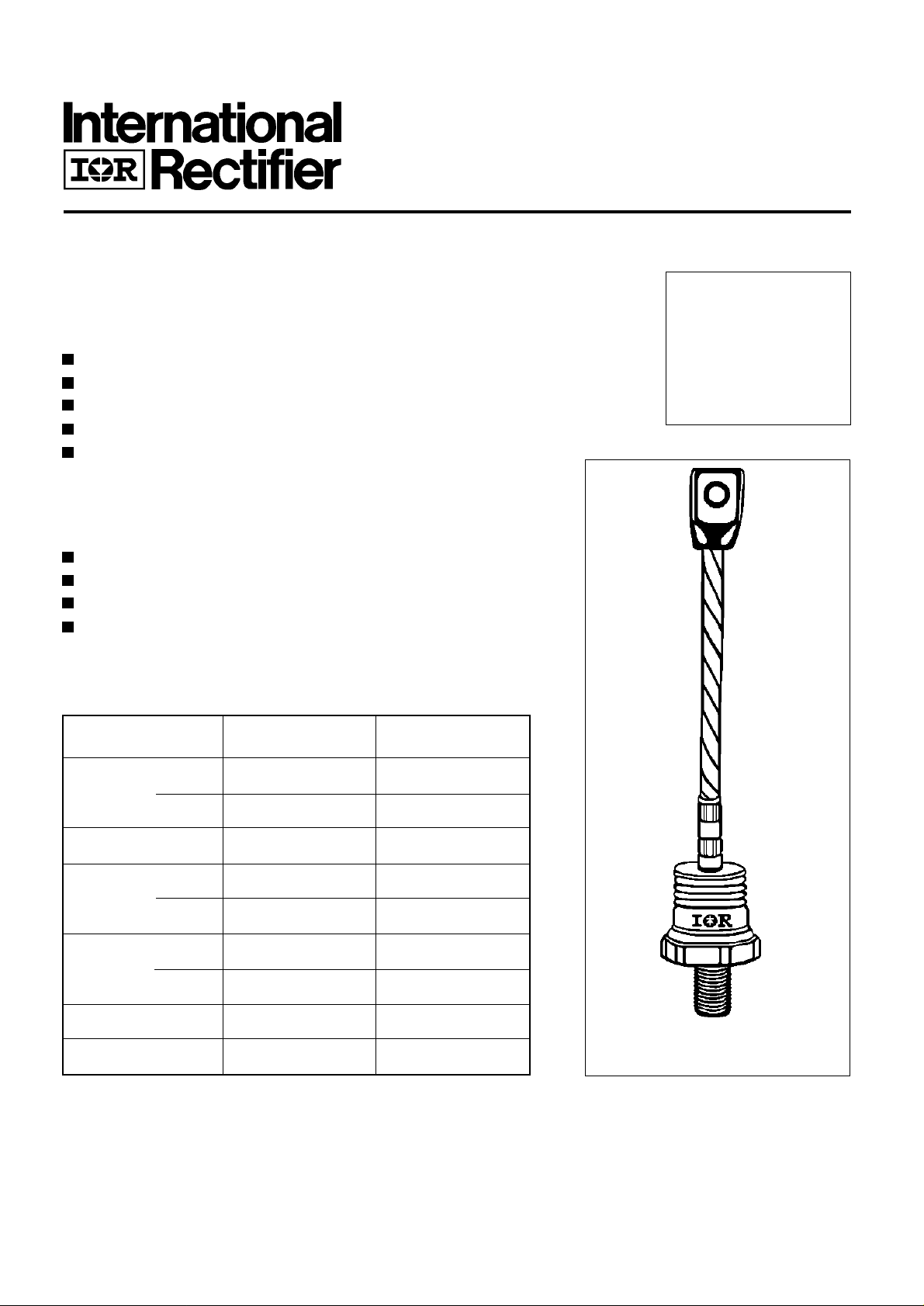
Stud V ersion
475A
Major Ratings and Characteristics
Parameters SD500N/R Units
I
F(AV)
@ T
C
I
F(RMS)
I
FSM
I2t@
V
RRM
T
J
@ 50Hz 7500 A
@ 60Hz 7850 A
50Hz 281 KA2s
@ 60Hz 257 KA2s
range 3000 to 4500 V
475 A
55 ° C
745 A
- 40 to 150 °C
case style
B-8
Page 2
SD500N/R Series
Next Data SheetIndex
Previous Datasheet
To Order
ELECTRICAL SPECIFICATIONS
Voltage Ratings
Voltage V
Type number Code peak reverse voltage repetitive peak rev. voltage @ T
30 3000 3100
SD500N/R 50
36 3600 3700
40 4000 4100
45 4500 4600
Forward Conduction
Parameter SD500N/R Units Conditions
, maximum repetitive V
RRM
VVmA
, maximum non- I
RSM
RRM
max.
= TJ max.
J
I
F(AV)
Max. average forward current 475 A 180° conduction, half sine wave
@ Case temperature 55 °C
I
F(AV)
Max. average forward current 300 A 180° conduction, half sine wave
@ Case temperature 100 °C
I
F(RMS)
I
FSM
Max. RMS forward current 745 A DC @ 40°C case temperature
Max. peak, one-cycle forward, 7500 t = 10ms No voltage
non-repetitive surge current 7850 t = 8.3ms reapplied
A
6310 t = 10ms 50% V
RRM
6600 t = 8.3ms reapplied Sinusoidal half wave,
2
t Maximum I2t for fusing 281 t = 10ms No voltage Initial TJ = TJ max.
I
257 t = 8.3ms reapplied
199 t = 10ms 50% V
KA2s
RRM
182 t = 8.3ms reapplied
2
√t Maximum I2√t for fusing 2810 KA2√s t = 0.1 to 10ms, no voltage reapplied
I
V
V
r
f
r
f
V
Low level value of threshold
F(TO)1
voltage
High level value of threshold
F(TO)2
voltage
Low level value of forward
1
0.88 (16.7% x π x I
V
0.97 (I > π x I
F(AV)
0.78 (16.7% x π x I
slope resistance
High level value of forward
2
slope resistance
Max. forward voltage drop 1.66 V Ipk= 1000A, TJ = TJ max, tp = 10ms sinusoidal wave
FM
0.72 (I > π x I
mΩ
F(AV)
< I < π x I
F(AV)
),TJ = TJ max.
< I < π x I
F(AV)
),TJ = TJ max.
), TJ = TJ max.
F(AV)
), TJ = TJ max.
F(AV)
Page 3

Thermal and Mechanical Specifications
To Order
Next Data SheetIndex
Previous Datasheet
Parameter SD500N/R Units Conditions
SD500N/R Series
T
T
R
R
to heatsink greased
T Max. allowed mounting torque ±10% 50 Nm Not lubricated threads
wt Approximate weight 454 g
∆R
(The following table shows the increment of thermal resistence R
Max. junction operating temperature range -40 to 150
J
Max. storage temperature range -55 to 200
stg
Max. thermal resistance, junction to case 0.1 DC operation
thJC
Max. thermal resistance, case Mounting surface, smooth, flat and
thCS
Case style B - 8 See Outline Table
Conduction
thJC
0.04
when devices operate at different conduction angles than DC)
thJC
°C
K/W
Conduction angle Sinusoidal conduction Rectangular conduction Units Conditions
180° 0.012 0.008 TJ = TJ max.
120° 0.014 0.014
90° 0.017 0.019
60° 0.025 0.026
30° 0.042 0.042
K/W
Ordering Information Table
Device Code
1 - Diode
2 - Essential part number
3 - 0 = Standard recovery
4 - N = Stud Normal Polarity (Cathode to Stud)
R = Stud Reverse Polarity (Anode to Stud)
5 - Voltage code: Code x 100 = V
6 - P = Stud base B-8 3/4" 16UNF-2A
M = Stud base B-8 M24 X 1.5
7 - S = Isolated lead with silicone sleeve
(Red = Reverse Polarity; Blue = Normal Polarity)
T = Threaded Top Terminal 3/8" 24UNF-2A
SD 50 0 N 45 P S C
1 23456
(See Voltage Ratings table)
RRM
7
8
None = Non isolated lead
8 - C = Ceramic Housing
NOTE: Available for rotating applications (Contact factory)
Page 4

SD500N/R Series
To Order
Next Data SheetIndex
Previous Datasheet
Outlines Table
CERAMIC HOUSING
12 (0.47) MIN.
DIA. MAX.
38 (1.5)
26 (1.023) MAX.
10.5 (0.41) DIA.
C.S. 70mm
SW 45
5(0.20) ± 0.3(0.01)
2
Case Style B-8
All dimensions in millimeters (inches)
3/4"-16UNF-2A *
* FOR METRIC DEVICE: M24 x 1.5 - SCREW LENGTH — 21(0.83) MAX.
CERAMIC HOUSING
Case Style B-8 with top thread terminal 3/8"
All dimensions in millimeters (inches)
17 (0.67) DIA.
3/8"-24UNF-2A
38 (1.5)
DIA. MAX.
SW 45
3/4"-16UNF-2A *
* FOR METRIC DEVICE: M24 x 1.5 - SCREW LENGTH — 21(0.83)
Page 5

SD500N/R Series
To Order
Next Data SheetIndex
Previous Datasheet
150
140
SD500N/R Series
R (DC) = 0.1 K/W
thJC
130
120
110
Conduction Angle
100
90
80
70
30°
60°
90°
60
50
Max imum Allowable Case Temperatur e (°C)
0 100 200 300 400 500
Average Forwar d Current (A )
Fig. 1 - Current Ratings Characteristics
900
800
180°
700
120°
90°
600
500
60°
30°
120°
180°
RMS Lim it
150
140
130
SD500N/R Series
R (DC) = 0 .1 K/W
thJC
120
110
100
Conduction P eri od
90
80
70
60
50
40
30
Max im um Al l owable Cas e Temperatu r e (°C )
0 100 200 300 400 500 600 700 800
30°
60°
90°
120°
180°
DC
Aver age Forwar d Current (A )
Fig. 2 - Current Ratings Characteristics
R
t
h
S
A
=
0
0
0
.
.
0
0
.
1
1
4
K
K
K
/W
/
/
W
W
-
D
e
l
t
a
R
M axim um Aver age Forward Power Loss (W)
400
300
Conduction Angle
200
100
0
M axim um Average For w ard Power L oss (W)
0 100 200 300 400 500
S D500N/ R S eries
T = 150°C
J
Average Forward Curr e nt (A)
Fig. 3 - Forward Power Loss Characteristics
1100
1000
900
800
700
600
DC
180°
120°
90°
60°
30°
RMS Lim it
500
400
Conduction P er i od
300
200
100
S D500N/ R S eries
T = 150°C
J
0
0 100 20 0 300 400 500 600 700 800
0
.
2
K
/
W
0
.
4
K
/
W
0
.
6
K
/
W
1
8
.
K
/
W
25 50 75 100 125 150
M aximum All owable Ambien t Tempe rature ( °C)
R
t
h
S
A
=
0
.
0
1
K
0
.
0
0
.
1
0
.
2
0
.
4
0
.
6
1
8
.
/
4
W
K
/
K
/
K
/
W
K
/
K
/
K
/
-
W
W
W
W
W
D
e
l
t
a
R
25 50 75 100 125 150
Aver age Forw ard Current (A)
Fig. 4 - Forward Power Loss Characteristics
M axim um Allowable Am b ient Temperature (°C)
Page 6

SD500N/R Series
To Order
Next Data SheetIndex
Previous Datasheet
8000
At Any Rated Load Condition An d Wit h
5 0% Rated V Applied Following Surge
7000
6000
5000
4000
3000
Peak Half Sine Wave Forwar d Curren t ( A)
2000
Nu mber Of Equal Amplitude Half Cycle Curr en t P u lses (N)
SD5 0 0N/ R Se rie s
110100
Fig. 5 - Maximum Non-Repetitive Surge Current
RRM
Initial T = 150 °C
J
@ 60 H z 0.0083 s
@ 50 H z 0.0100 s
10000
Peak Hal f Sine Wave Forwar d Cur rent (A)
9000
8000
7000
6000
5000
4000
3000
2000
1000
Maximum Non Repetitive Surge Cu r r en t
Versus Pulse Train D u r ation.
Initial T = 150°C
No Voltage Reapplied
5 0% Rated V Reappl ied
SD500N/R Series
0.01 0.1 1
Pulse Train Duration (s)
Fig. 6 - Maximum Non-Repetitive Surge Current
RRM
J
T = 25 ° C
J
T = 150°C
1000
Instantaneous For ward Cur rent (A)
100
0.511.522.533.54
Instantaneous F orward Vol tage (V)
Fig. 7 - Forward Voltage Drop Characteristics
1
thJ C
0.1
Steady State Val u e:
R = 0.1 K/W
thJC
(DC O perati on)
J
SD500N/R S eries
0.01
Transient Therm al Impedance Z ( K/W)
0.001
0.001 0.01 0.1 1 10
Square Wav e Pulse D uration (s)
Fig. 8 - Thermal Impedance Z
SD500 N/R Series
Characteristics
thJC
 Loading...