Page 1

CURRENT MODE PWM CONTROLLER
DESCRIPTION
SD4870 is a current mode PWM controller IC for high performance,
low standby power offline flyback converter application.
In no load or light load condition, the IC operates in Light Load
Mode to reduce switching loss and improve efficiency.
Large value startup resistor could be used in the startup circuit to
minimize the standby current because of low startup current.
SD4870 offers complete protection functions including cycle-by-
cycle over current protection, over load protection, V
over voltage and under voltage protection, etc.
Excellent EMI performance is achieved with frequency shuffling
technique and soft switching control at the totem pole gate driver
output.
DD voltage
SD4870_Datasheet
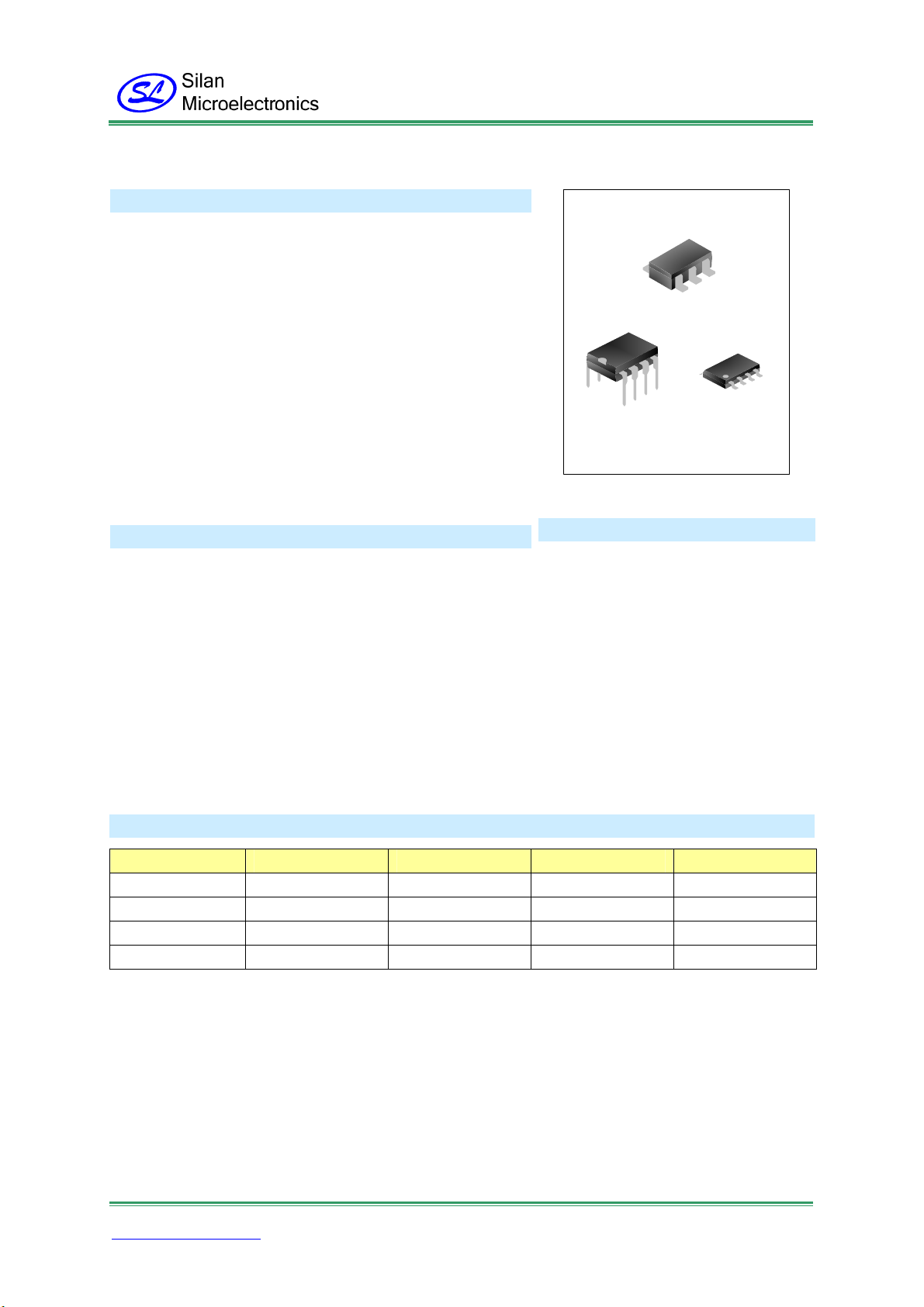
SOT-23-6L
SOP-8-225-1.27DIP-8-300-2.54
FEATURES
* Frequency shuffling to improve EMI performance
* Light Load Mode for minimum standby power
* External programmable switching frequency
* 3uA low startup current
* Internal LEB circuit
DD over voltage and under voltage protection
* V
* Gate output maximum voltage clamp
* Current limiting
* Over load protection
* SOT-23-6L/SOP8/DIP8 package
APPLICATIONS
* Battery Chargers
* Adapters
* Set-Top Box Power Supplies
ORDERING INFORMATION
Part No. Package Marking Material Packing
SD4870TR SOT-23-6L 4870 Pb free Tape & Reel
SD4870A DIP-8-300-2.54 SD4870A Pb free Tube
SD4870C SOP-8-225-1.27 SD4870C Pb free Tube
SD4870CTR SOP-8-225-1.27 SD4870C Pb free Tape & Reel
HANGZHOU SILAN MICROELECTRONICS CO.,LTD
Http://www.silan.com.cn Page 1 of 9
REV:1.3 2010.12.29
Page 2

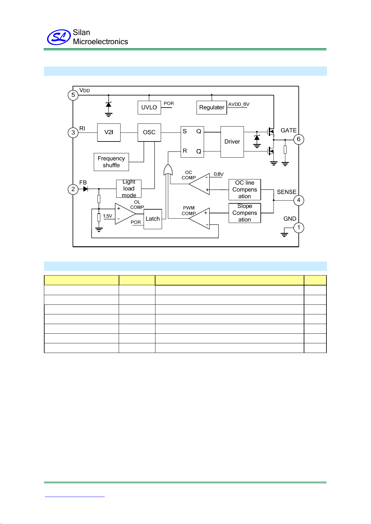
BLOCK DIAGRAM
SD4870_Datasheet
ABSOLUTE MAXIMUM RATINGS
Characteristics Symbol Rating Unit
VDD Voltage VVDD 25 V
FB Voltage VFB -0.3~6 V
SENSE Voltage VSENSE -0.3~6 V
RI Voltage VRI -0.3~6 V
Junction Temperature Tj -20~150 °C
Lead Temperature TL 260 °C
Storage Temperature Tstg -55~160 °C
HANGZHOU SILAN MICROELECTRONICS CO.,LTD
Http://www.silan.com.cn Page 2 of 9
REV:1.3 2010.12.29
Page 3

SD4870_Datasheet
ELECTRICAL CHARACTERISTICS (Unless otherwise specified, Tamb=25°C)
Characteristics Symbol Test Condition
VDD
Startup Current IVDD_ST VDD=12 V,RI=100kΩ -- 3 20 μA
DD=16V, VFB =3V,
Operation Current IVDD
UVLO Threshold Voltage VUVLO 13.3 14.3 15.3 V
UVLO Hysteresis Voltage VUVLOH -- 6.3 -- V
VDD Clamp Voltage VVDD_CLP IVDD =10mA -- 21.5 -- V
Feedback
PWM Gain AVCS ΔVFB /ΔVSENSE -- 2 -- V/V
FB Open Loop Voltage
FB Short Circuit Current IFB_SHORT
FB OL Threshold Voltage VFB_OL -- 3.8 -- V
OL Debounce Time TD_OL 35 -- ms
FB Input Impedance ZFB_IN 4 6 -- kΩ
Maximum Duty Cycle DMAX
Current Sense
LEB Time TLEB RI=100kΩ -- 300 -- ns
SENSE Input Impedance ZSENSE_IN -- 85 -- kΩ
OC Control Delay TOC -- 75 -- ns
OC Detection Threshold VSENSE_OC 0.7 0.75 0.8 V
Switching Frequency
Ocsillation Frequency fS RI=100kΩ 60 65 70 kHz
Frequency Stability With
DD
V
RI External Resistance
Range
Light Load Mode
Frequency
Frequency Shuffling Range ΔfS_SHUF RI=100kΩ -3 -- 3 %
Gate Driver
Output Low Level VOL VDD=16V, IO=-20mA -- -- 0.8 V
Output High Level VOH VDD=16V, IO=20mA 10 -- -- V
Output Clamp Voltage
Level
Output Rising Time TR VDD=16V,CL=1nF -- 220 -- ns
Output Falling Time TF VDD=16V,CL=1nF -- 70 -- ns
B_OPEN
VF
S_VDD VDD=12~25V,RI=100kΩ -- 5 -- %
Δf
R
RI_RANGE
f
S_LLM
V
OH_CLAMP
V
I=100kΩ
R
FB short connected to
nd
grou
DD=16V, RI=100kΩ
V
FB =3V,VSENSE =0V
V
Min. Typ. Max.
-- 2 -- mA
4.5 4.8 5 V
0.8 1 1.2 mA
-- 75 -- %
50 100 150 kΩ
-- 22 -- kHz
-- 13 -- V
Unit
HANGZHOU SILAN MICROELECTRONICS CO.,LTD
Http://www.silan.com.cn Page 3 of 9
REV:1.3 2010.12.29
Page 4

PIN CONFIGURATION
PIN DESCRIPTIONS
Pin No.
SD4870
1
2
3
4
5
6
SD4870A
SD4870C
8
7
5
4
2
1
3,6
Pin Name I/O Description
GND -- Ground.
FB I Feedback input pin.
RI I/O
SENSE I Switch current sense input pin.
VDD -- Power supply pin.
GATE O Gate driver output pin.
NC -- Not connect
Oscillator frequency setting pin.
A resistor connected between RI and GND.
SD4870_Datasheet
FUNCTION DESCRIPTIONS
SD4870 is a current mode PWM controller used in applications for offline flyback converter. The description of
functions is as follows.
Startup Control
Startup current of SD4870 is very low so that IC could start up quickly. A large value startup resistor can be used
in startup circuit to minimize standby power loss yet provides reliable startup in application.
A 2 MΩ, 1/8 W startup resistor is recommended in normal input range.
Frequency Shuffling Control
Frequency shuffling is used in SD4870 to improve EMI performance.
The oscillation frequency is modulated with a random sourse so that the tone energe is spread out. The spead
spectrum minmizes the conduction band EMI and the system design can be easier.
The entire application system design can become simpler.
HANGZHOU SILAN MICROELECTRONICS CO.,LTD
Http://www.silan.com.cn Page 4 of 9
REV:1.3 2010.12.29
Page 5

SD4870_Datasheet
Light Load Mode
In no load or light load condition, major power loss of total power consumption is from switching loss on the
MOSFET transistor switching loss, the core loss of the transformer loss and the loss on the external snubber
circuit loss become the majority in total power loss. The value of those power loss is proportional to switching
actions within a fixed period of time. So reducing number of switching actions leads to reduction of power loss.
SD4870 enters Light Load Mode in no load or light load condition. The gate drive output switches only when
output DC voltage drops below a present level and the switching frequency reduces. Otherwise the gate drive
remains at off state.
Oscillation Frequency Setting
The oscillation frequency is determined by resistor connected between RI and GND. The relationship between
the value of this resistor and frequency are shown below
6500
f
=
S
R
RI
, where RRI is the value of external resistor and its unit is KΩ.
(kHz)
Current Sense and LEB
At switching leading edge time, the current spike due to Snubber diode reverse recovery should be chopped off.
And this is available through internal LEB (Leading Edge Blanking) circuit. So that the external RC filter circuit on
SENSE input is no longer required.
During the blanking period, the PWM comparator and OC comparator are disabled and MOSFET transistor
keeps turn-on state if MOSFET turns on. The minimum on time of MOSFET is LEB time.
Gate Drive
GATE pin is connected to external MOSFET’s gate for switch control. Too weak the gate drive ability results in
more switch loss of MOSFET while too strong gate drive compromises the EMI performance.
A good tradeoff is achieved through the totem pole gate drive design with appropriate output ability and dead
time control.
Protection controls
SD4870 offers complete protection functions including cycle-by-cycle over current protection, over load protection,
DD input voltage over voltage and under voltage protection, etc.
V
Constant output power limit over universal input voltage range is achived with over current protection threshold
line voltage compensation to over current protection threshold.
DD is supplies by transformer auxiliary winding output. It is clamped when VDD is higher than clamp threshold
V
value. The MOSFET is shut down when V
DD drops below UVLO threshold voltage and IC enters power on
startup sequence thereafter.
When FB input voltage is higher than over load threshold voltage for more than T
down and V
DD voltage drops. IC restarts when VDD is lower than UVLO threshold voltage.
D_OL, the MOSFET is shut
HANGZHOU SILAN MICROELECTRONICS CO.,LTD
REV:1.3 2010.12.29
Http://www.silan.com.cn Page 5 of 9
Page 6

TYPICAL APPLICATION CIRCUIT
SD4870_Datasheet
HANGZHOU SILAN MICROELECTRONICS CO.,LTD
Http://www.silan.com.cn Page 6 of 9
REV:1.3 2010.12.29
Page 7

SD4870_Datasheet
PACKAGE OUTLINE
DIP-8-300-2.54 UNIT: mm
SOP-8-225-1.27 UNIT: mm
6.0±0.4
1.55±0.20
3.9±0.3
5.72±0.3
0.3~1.27
HANGZHOU SILAN MICROELECTRONICS CO.,LTD
Http://www.silan.com.cn Page 7 of 9
REV:1.3 2010.12.29
Page 8

SD4870_Datasheet
PACKAGE OUTLINE
SOT-23-6L UNIT: mm
MOS DEVICES OPERATE NOTES:
Electrostatic charges may exist in many things. Please take following preventive measures to prevent effectively
the MOS electric circuit as a result of the damage which is caused by discharge:
z The operator must put on wrist strap which should be earthed to against electrostatic.
z Equipment cases should be earthed.
z All tools used during assembly, including soldering tools and solder baths, must be earthed.
z MOS devices should be packed in antistatic/conductive containers for transportation.
Disclaimer :
• Silan reserves the right to make changes to the information herein for the improvement of the design and
performance without further notice! Customers should obtain the latest relevant information before placing
orders and should verify that such information is complete and current.
• All semiconductor products malfunction or fail with some probability under special conditions. When using
Silan products in system design or complete machine manufacturing, it is the responsibility of the buyer to
comply with the safety standards strictly and take essential measures to avoid situations in which a
malfunction or failure of such Silan products could cause loss of body injury or damage to property.
• Silan will supply the best possible product for customers!
HANGZHOU SILAN MICROELECTRONICS CO.,LTD
Http://www.silan.com.cn Page 8 of 9
REV:1.3 2010.12.29
Page 9

SD4870_Datasheet
ATTACHMENT
Revision History
Date REV Description Page
2009.08.24 1.0 Original
2009.09.22 1.0 Modify the” ELECTRICAL CHARACTERISTICS”
2009.12.23 1.0 Modify the” FEATURES”
2010.05.27 1.1 Modify the” BLOCK DIAGRAM”
2010.08.17 1.2 Modify ”DESCRIPTIN”, “FEATURES”
2010.12.29 1.3 Modify the template of datasheet
HANGZHOU SILAN MICROELECTRONICS CO.,LTD
Http://www.silan.com.cn Page 9 of 9
REV:1.3 2010.12.29
Page 10

 Loading...