

Page 1
Vishay High Power Products
Fast Recovery Diodes
(Hockey PUK Version), 430 A
FEATURES
• High power FAST recovery diode series
SD403C..C Series
• 1.0 to 1.5 µs recovery time
• High voltage ratings up to 1600 V
• High current capability
• Optimized turn-on and turn-off characteristics
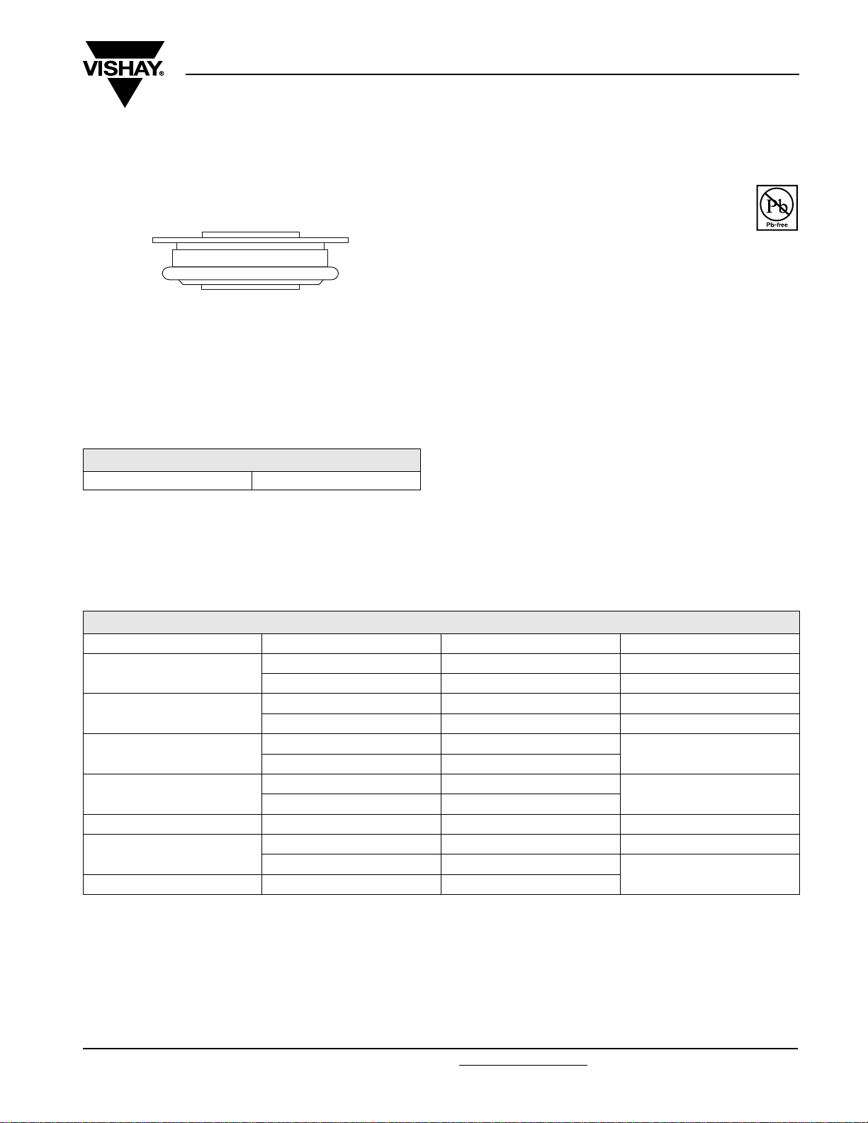
DO-200AA
• Low forward recovery
• Fast and soft reverse recovery
• Press PUK encapsulation
• Case style conform to JEDEC DO-200AA
• Maximum junction temperature 125 °C
PRODUCT SUMMARY
I
F(AV)
430 A
• Lead (Pb)-free
TYPICAL APPLICATIONS
• Snubber diode for GTO
• High voltage freewheeling diode
• Fast recovery rectifier applications
MAJOR RATINGS AND CHARACTERISTICS
PARAMETER TEST CONDITIONS VALUES UNITS
I
F(AV)
I
F(RMS)
I
FSM
2
I
t
V
RRM
t
rr
T
J
T
hs
T
hs
50 Hz 6180
60 Hz 6470
50 Hz 191
60 Hz 175
Range 400 to 1600 V
T
J
430 A
55 °C
675 A
25 °C
1.0 to 1.5 µs
25
- 40 to 125
A
kA2s
°C
RoHS
COMPLIANT
Document Number: 93175 For technical questions, contact: ind-modules@vishay.com
Revision: 04-Aug-08 1
www.vishay.com
Page 2
SD403C..C Series
Vishay High Power Products
Fast Recovery Diodes
(Hockey PUK Version), 430 A
ELECTRICAL SPECIFICATIONS
VOLTAGE RATINGS
V
, MAXIMUM REPETITIVE PEAK
TYPE NUMBER
VOLTAGE
CODE
RRM
AND OFF-STATE VOLTAGE
V
04 400 500
SD403C..S10C
08 800 900
10 1000 1100
12 1200 1300
SD403C..S15C
14 1400 1500
16 1600 1700
FORWARD CONDUCTION
PARAMETER SYMBOL TEST CONDITIONS VALUES UNITS
Maximum average forward current
at heatsink temperature
Maximum RMS current I
F(RMS)
Maximum peak, one-cycle ,
non-repetitive forward current
Maximum I
Maximum I
2
t for fusing I2t
2
√t for fusing I2√t t = 0.1 to 10 ms, no voltage reapplied 1910 kA2√s
Low level value of threshold voltage V
High level value of threshold voltage V
Low level of forward slope resistance r
High level of forward slope resistance r
Maximum forward voltage drop V
I
F(AV)
I
FSM
F(TO)1
F(TO)2
180° conduction, half sine wave
Double side (single side) cooled
25 °C heatsink temperature double side cooled 675
t = 10 ms
t = 8.3 ms 6470
t = 10 ms
t = 8.3 ms 5445
t = 10 ms
t = 8.3 ms 175
t = 10 ms
t = 8.3 ms 123
(16.7 % x π x I
(I > π x I
(16.7 % x π x I
f1
(I > π x I
f2
Ipk = 1350 A, TJ = 25 °C; tp = 10 ms sinusoidal wave 1.83 V
FM
No voltage
reapplied
100 % V
reapplied
No voltage
reapplied
100 % V
reapplied
F(AV)
), TJ = TJ maximum 1.20
F(AV)
F(AV)
), TJ = TJ maximum 0.70
F(AV)
V
RRM
RRM
< I < π x I
< I < π x I
, MAXIMUM NON-REPETITIVE
RSM
PEAK VOLTAGE
V
Sinusoidal half wave,
initial T
= TJ maximum
J
), TJ = TJ maximum 1.00
F(AV)
), TJ = TJ maximum 0.56
F(AV)
I
MAXIMUM
RRM
= 125 °C
AT T
J
mA
35
430 (210) A
55 (75) °C
6180
5200
191
135
kA
mΩ
A
2
s
V
RECOVERY CHARACTERISTICS
TYPICAL VALUES
AT TJ = 125 °C
RRM
(µs)
Q
(µC)
rr
2.4 52 33
I
(A)
I
FM
rr
t
rr
I
RM(REC)
t
Q
rr
dir
dt
Document Number: 93175
CODE
MAXIMUM VALUE
= 25 °C
AT T
J
AT 25 % I
t
rr
RRM
(µs)
TEST CONDITIONS
I
pk
SQUARE
PULSE
dI/dt
(A/µs)
V
(V)
r
t
AT 25 % I
rr
(A)
S10 1.0
S15 1.5 2.9 90 44
750 25 - 30
www.vishay.com For technical questions, contact: ind-modules@vishay.com
2 Revision: 04-Aug-08
Page 3

SD403C..C Series
Fast Recovery Diodes
Vishay High Power Products
(Hockey PUK Version), 430 A
THERMAL AND MECHANICAL SPECIFICATIONS
PARAMETER SYMBOL TEST CONDITIONS VALUES UNITS
Maximum operating temperature range T
Maximum storage temperature range T
Maximum thermal resistance,
junction to heatsink
Mounting force, ± 10 % 4900 (500) N (kg)
Approximate weight 70 g
Case style
ΔR
CONDUCTION ANGLE
Note
• The table above shows the increment of thermal resistance R
CONDUCTION
thJ-hs
SINUSOIDAL CONDUCTION RECTANGULAR CONDUCTION
SINGLE SIDE DOUBLE SIDE SINGLE SIDE DOUBLE SIDE
180° 0.010 0.011 0.008 0.008
120° 0.012 0.013 0.013 0.013
90° 0.016 0.016 0.018 0.018
60° 0.024 0.024 0.025 0.025
30° 0.042 0.042 0.042 0.042
R
J
Stg
thJ-hs
DC operation single side cooled 0.16
DC operation double side cooled 0.08
See dimensions - link at the end of
datasheet
when devices operate at different conduction angles than DC
thJ-hs
- 40 to 125
- 40 to 150
DO-200AA
TEST CONDITIONS UNITS
T
= TJ maximum K/W
J
°C
K/W
Document Number: 93175 For technical questions, contact: ind-modules@vishay.com
Revision: 04-Aug-08 3
www.vishay.com
Page 4

SD403C..C Series
Vishay High Power Products
130
120
110
100
90
80
70
0 50 100 150 200 250
Maxim um Allowable Heatsink Tempe rature (°C )
Fig. 1 - Current Ratings Characteristics
130
120
110
100
90
80
70
60
50
0 50 100 150 200 250 300 350
Maximum Allowable Heatsink Temperature (°C)
Fig. 2 - Current Ratings Characteristics
SD 403C ..C Series
(Single Side C oo le d )
R (D C ) = 0.16 K/W
thJ- hs
Conduction Angle
60°
30°
Average Forward Current (A)
SD 403C ..C Serie s
(Single Side Coo led )
R (D C ) = 0 .1 6 K /W
thJ-h s
30°
60°
Average Forward Current (A)
90°
Conduction Period
90°
120°
180°
120°
Fast Recovery Diodes
(Hockey PUK Version), 430 A
180°
Maximum A llow able Heatsink Temperature (°C)
DC
Max imum Av erage Forw ar d Pow er Loss (W )
130
120
110
100
90
80
70
60
50
40
0 100 200 300 400 500 600 700
SD 4 03C ..C Se ries
(Doub le Side Coole d)
R (DC ) = 0.08 K/W
thJ-h s
Conduction Period
90°
60°
30°
Average Forw ard Current (A)
120°
180°
DC
Fig. 4 - Current Ratings Characteristics
800
700
600
500
400
300
200
100
180°
120°
90°
60°
30°
0
0 50 100 150 200 250 300 350 400 450
Average Forward Current (A)
RMS Limit
Conduction Angle
SD403C..C Series
T = 125°C
J
Fig. 5 - Forward Power Loss Characteristics
130
120
110
100
90
80
70
60
50
0 50 100 150 200 250 300 350 400 450
Maxim um Allowable Heatsink Temperature (°C)
SD403C..C Series
(Doub le Side Co oled)
R (DC ) = 0 . 08 K / W
th J-hs
Conduction Angle
30°
60°
90°
Average Forward Current (A)
Fig. 3 - Current Ratings Characteristics
120°
180°
1100
1000
Maximum Average Forward Power Loss (W )
DC
180°
900
120°
800
90°
60°
700
30°
600
RM S Lim it
500
400
300
200
100
0
0 100 20 0 300 4 0 0 500 600 7 00
Average Forw ard Current (A)
Conduction Period
SD40 3C ..C S eries
T = 125°C
J
Fig. 6 - Forward Power Loss Characteristics
www.vishay.com For technical questions, contact: ind-modules@vishay.com
Document Number: 93175
4 Revision: 04-Aug-08
Page 5

SD403C..C Series
Fast Recovery Diodes
(Hockey PUK Version), 430 A
6000
At Any Rated Load Condition And W ith
R a te d V A p p li e d Fo ll o w in g S u rg e.
5500
5000
4500
4000
3500
3000
2500
Peak Half Sine W ave Forw ard Current (A)
2000
Num ber Of Equal Amplitud e Half Cycle Current Pulses (N)
Fig. 7 - Maximum Non-Repetitive Surge Current
Single and Double Side Cooled
700 0
Maxim um Non Repetitive Surge Current
600 0
500 0
RRM
SD403C..C Series
Versus Pulse Train Duration.
In it i a l T = 1 25 ° C
J
@ 60 Hz 0.0083 s
@ 50 Hz 0.0100 s
Initial T = 125°C
J
No Voltage Reapplied
Rated V Reapplied
RRM
Vishay High Power Products
1
SD 403 C..C S erie s
0.1
thJ-h s
Steady State Value
R = 0 . 1 6 K /W
0.01
001011
0.001
Transient Therm al Im ped ance Z (K/W)
0.001 0.01 0.1 1 10 100
Sq ua re W ave P ulse D ura tion (s)
Fig. 10 - Thermal Impedance Z
2.8
2.6
2.4
thJ-hs
(Single Side Coo led )
R = 0 . 0 8 K /W
thJ- hs
(Double Side Cooled)
(D C O p e ra tion)
thJ-hs
SD 4 0 3C ..S10C Se ries
T = 125 °C ; V = 30V
J
r
I = 750 A
FM
Squa re Pulse
Characteristics
400 0
300 0
200 0
SD 403C . .C Se r ies
Peak Half Sine Wave Forward Current (A)
100 0
11.010.0
Pulse Train Duration (s)
Fig. 8 - Maximum Non-Repetitive Surge Current
Single and Double Side Cooled
10000
T = 25 °C
J
T = 125 °C
J
1000
100
Ins tan ta neo u s Fo rw ard Curr ent (A )
10
01234567
Instantan eo us Fo rw ar d V o ltage (V)
SD403C..C Series
Fig. 9 - Forward Voltage Drop Characteristics
2.2
2
1.8
Maximum Re verse Recovery Time - Trr (µs)
1.6
Rate Of Fall Of Forward Current - di/dt (A/µs)
400 A
200 A
00101
Fig. 11 - Recovery Time Characteristics
140
130
120
110
100
90
80
70
60
50
40
30
20
10
0 20406080100
Maximum Reverse Recovery Charge - Qrr (µC)
Rate Of Fall Of Forward C urrent - di/dt (A/µs)
I = 75 0 A
FM
Squa re Pulse
400 A
200 A
SD 40 3C ..S10 C Se rie s
T = 12 5 °C ; V = 30 V
J
r
Fig. 12 - Recovery Charge Characteristics
Document Number: 93175 For technical questions, contact: ind-modules@vishay.com
www.vishay.com
Revision: 04-Aug-08 5
Page 6

SD403C..C Series
Vishay High Power Products
90
I = 750 A
FM
80
Sq ua re P u lse
70
60
50
40
30
20
10
Maximum Reverse Recovery Current - Irr (A)
Rate Of Fall O f Forward Current - di/dt (A/µs)
Fig. 13 - Recovery Current Characteristics
3.5
3
2.5
2
Maximum Reve rse Recovery Time - Trr (µs)
1.5
Rate Of Fall Of Forward Current - di/dt (A/µs)
Fig. 14 - Recovery Time Characteristics
400 A
200 A
SD403C..S10C Series
T = 125 °C ; V = 30V
J
10 20 30 4 0 50 60 70 80 90 100
SD 403C ..S15C Serie s
T = 125 °C; V = 30V
J
r
r
I = 750 A
FM
Sq uare Pulse
400 A
200 A
Fast Recovery Diodes
(Hockey PUK Version), 430 A
Rate Of Fall Of Forward Current - di/dt (A/µs)
Fig. 15 - Recovery Charge Characteristics
00101
Rate Of Fall Of Forward C urrent - di/dt (A/µs)
Fig. 16 - Recovery Current Characteristics
170
160
150
140
130
120
110
100
90
80
70
60
50
0 20406080100
M a xim u m Re verse R e co ve ry C h a rg e - Qrr ( µC )
130
120
110
100
90
80
70
60
50
40
30
20
10
Maximum Reverse Recovery Current - Irr (A)
10 20 30 40 5 0 60 70 80 9 0 100
I = 75 0 A
FM
Sq ua re P u ls e
400 A
200 A
SD40 3C..S15C Serie s
T = 12 5 ° C ; V = 30V
J
I = 750 A
FM
Sq uare P u lse
SD403C..S15C Series
T = 12 5 °C; V = 30V
J
r
400 A
200 A
r
1E4
1
0.4
1E3
1E2
Pe a k F o rw a r d C urre n t (A )
tp
1E1
1E1 1E2 1E3 1E4
0.2
0.1
0.04
0.02
0.01
SD403 C ..S10C Series
Sinu soida l Pul se
T = 12 5°C, V = 80 0V
J
dv/dt = 1000V/µs
RRM
Pulse Basew idth (µs)
4
2
20 jo u le s p e r p ulse
10
20 jo ul e s p er p ul se
10
4
2
1
0.4
0.2
0.1
0.04
SD403C..S10C Series
Trapezoidal Pulse
T = 12 5° C, V = 80 0V
tp
dv/dt = 1000V/µs; d i/dt=50A/µs
RRM
J
1E11E21E31E4
Pulse Basew idth (µs)
Fig. 17 - Maximum Total Energy Loss Per Pulse Characteristics
www.vishay.com For technical questions, contact: ind-modules@vishay.com
Document Number: 93175
6 Revision: 04-Aug-08
Page 7

SD403C..C Series
(Hockey PUK Version), 430 A
1E4
2
1
0.4
1E3
1E2
Peak Forward Current (A)
tp
1E1
1E1 1 E2 1E3 1E4
0.2
0.1
0.04
0.02
SD4 03..S15C Seri es
Si nus oida l Pu ls e
T = 125°C, V = 1 120 V
J
dv/dt = 1000V/µs
Pulse Ba se w id th (µs)
RRM
ORDERING INFORMATION TABLE
Device code
20 joules per pulse
10
4
Fig. 18 - Maximum Total Energy Per Pulse Characteristics
SD 40 3 C 16 S15 C
Fast Recovery Diodes
1E1 1E2 1E3 1E4
Vishay High Power Products
20 joules per pulse
10
4
2
1
0.4
0.2
0.1
SD403C..S15C Series
Trapezoidal Pulse
T = 125°C, V = 11 20V
tp
dv/dt = 1000V/µs; di/dt=50A/µs
RRM
J
Pulse Basew idth (µs)
51324
1
- Diode
2
- Essential part number
3
- 3 = Fast recovery
4
- C = Ceramic PUK
5
- Voltage code x 100 = V
6
-trr code (see Recovery Characteristics table)
7
- C = PUK case DO-200AA
(see Voltage Ratings table)
RRM
67
Document Number: 93175 For technical questions, contact: ind-modules@vishay.com
www.vishay.com
Revision: 04-Aug-08 7
Page 8

DIMENSIONS in millimeters (inches)
3.5 (0.14) ± 0.1 (0.004) DIA. NOM. x
1.8 (0.07) deep MIN. both ends
Outline Dimensions
Vishay High Power Products
DO-200AA
42 (1.65) DIA. MAX.
19 (0.75) DIA. MAX.
2 places
38 (1.50) DIA. MAX.
Quote between upper and lower pole pieces has to be considered after
application of mounting force (see Thermal and Mechanical Specifications)
0.3 (0.01) MIN.
both ends
14.4 (0.57)
13.7 (0.54)
Document Number: 95248 For technical questions concerning discrete products, contact: diodes-tech@vishay.com
Revision: 06-Nov-07 For technical questions concerning module products, contact: ind-modules@vishay.com
www.vishay.com
1
Page 9

Legal Disclaimer Notice
Vishay
Disclaimer
All product specifications and data are subject to change without notice.
Vishay Intertechnology, Inc., its affiliates, agents, and employees, and all persons acting on its or their behalf
(collectively, “Vishay”), disclaim any and all liability for any errors, inaccuracies or incompleteness contained herein
or in any other disclosure relating to any product.
Vishay disclaims any and all liability arising out of the use or application of any product described herein or of any
information provided herein to the maximum extent permitted by law. The product specifications do not expand or
otherwise modify Vishay’s terms and conditions of purchase, including but not limited to the warranty expressed
therein, which apply to these products.
No license, express or implied, by estoppel or otherwise, to any intellectual property rights is granted by this
document or by any conduct of Vishay.
The products shown herein are not designed for use in medical, life-saving, or life-sustaining applications unless
otherwise expressly indicated. Customers using or selling Vishay products not expressly indicated for use in such
applications do so entirely at their own risk and agree to fully indemnify Vishay for any damages arising or resulting
from such use or sale. Please contact authorized Vishay personnel to obtain written terms and conditions regarding
products designed for such applications.
Product names and markings noted herein may be trademarks of their respective owners.
Document Number: 91000 www.vishay.com
Revision: 18-Jul-08 1
 Loading...