

Page 1
HF/VHF/UHF N-CHANNEL MOSFETs
■ GOLDMETALLIZATION
■ EXCELLENTTHERMALSTABILITY
■ COMMONSOURCE CONFIGURATION
■ P
DESCRIPTION
The SD2918is a gold metallizedN-ChannelMOS
field-effect RF power transistor. It is intended for
use in 50 V DC large signal applications up to
200 MHz
= 30 W MIN. WITH 18 dB GAIN@ 30
out
MHz
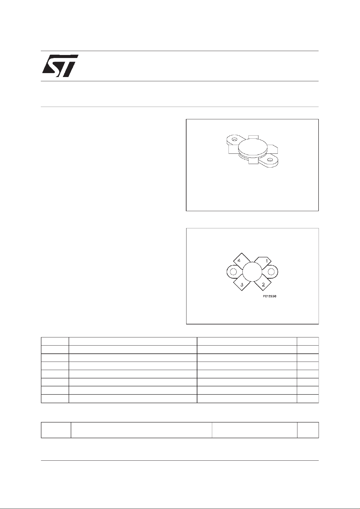
SD2918
RF POWER TRANSISTORS
ADVANCE DATA
M113
epoxy sealed
ORDER CODE BRANDING
SD2918 TSD2918
PIN CONNECTION
1. Drain 3.Gate
2. Source 4. Source
ABSOLUTE MAXIMUM RATINGS (T
Symb o l Para meter Val u e Uni t
V
(BR)DSS
V
V
P
T
Drain S our ce Vo lt age 125 V
Drain-Gate Voltage (RGS=1MΩ)
DGR
Gat e- Source Voltage ±20 V
GS
Drain C urr ent 6 A
I
D
Power Di ss ipation 175 W
DISS
Max. Operating Junction Te mperatur e 200
T
j
Sto rage T empe r ature -65 to 1 50
STG
case
=25oC)
125 V
THERMAL DATA
R
th(j-c)
R
th(c-s)
* Determined using a flat aluminum or copperheatsink with thermal compound applied (Dow Corning 340 or equivalent).
November 1999
Junct ion-Case Ther mal R esista nce
Case-Heatsink T her mal Resistance ∗
1.0
0.30
o
o
o
C/W
o
C/W
C
C
1/8
Page 2
SD2918
ELECTRICAL SPECIFICATION (T
case
=25oC)
STATIC
Symbol Para met e r Mi n . Typ . Ma x. Unit
V
(BR)DSSVGS
I
DSS
I
GSS
V
GS(Q)
V
DS(ON)VGS
g
FS
C
ISS
C
OSS
C
RSS
=0V IDS= 10 mA 125 V
VGS=0V VDS=50V 1.0 mA
VGS=20V VDS=0V 1 µA
VDS=10V ID=10mA 1.0 5.0 V
=10V ID= 2.5 A 5.0 V
VDS=10V ID=2.5A 0.8 mho
VGS=0V VDS=50V f=1MHz 58 pF
VGS=0V VDS=50V f=1MHz 35.5 pF
VGS=0V VDS=50V f=1MHz 7.5 pF
REF. 1022497C
DYNAMIC
Symbol Para met e r Mi n . Typ . Ma x. Unit
P
OUT
G
η
Load
Mismatch
f = 30M Hz VDD=50V Pin=0.475W IDQ=100mA 30 W
f = 30M Hz VDD=50V P
PS
f = 30M Hz VDD=50V P
D
f = 30M Hz V
=50V P
DD
=30W IDQ= 100 mA 18 22 dB
out
=30W IDQ= 100 mA 50 55 %
out
=30W IDQ=100mA
out
30:1 VSWR
All Angles
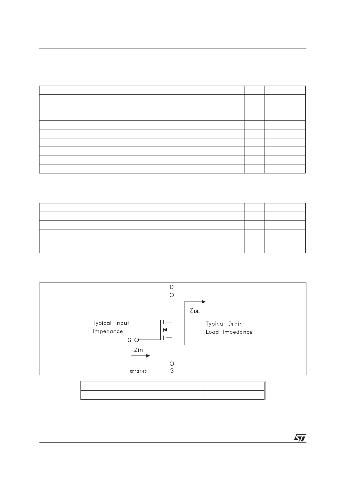
IMPEDANCEDATA
2/8
FREQ. ZIN(Ω)Z
DL
(Ω)
30 MHz 24.4 - j 13. 4 28.8 + j 7.2
Page 3
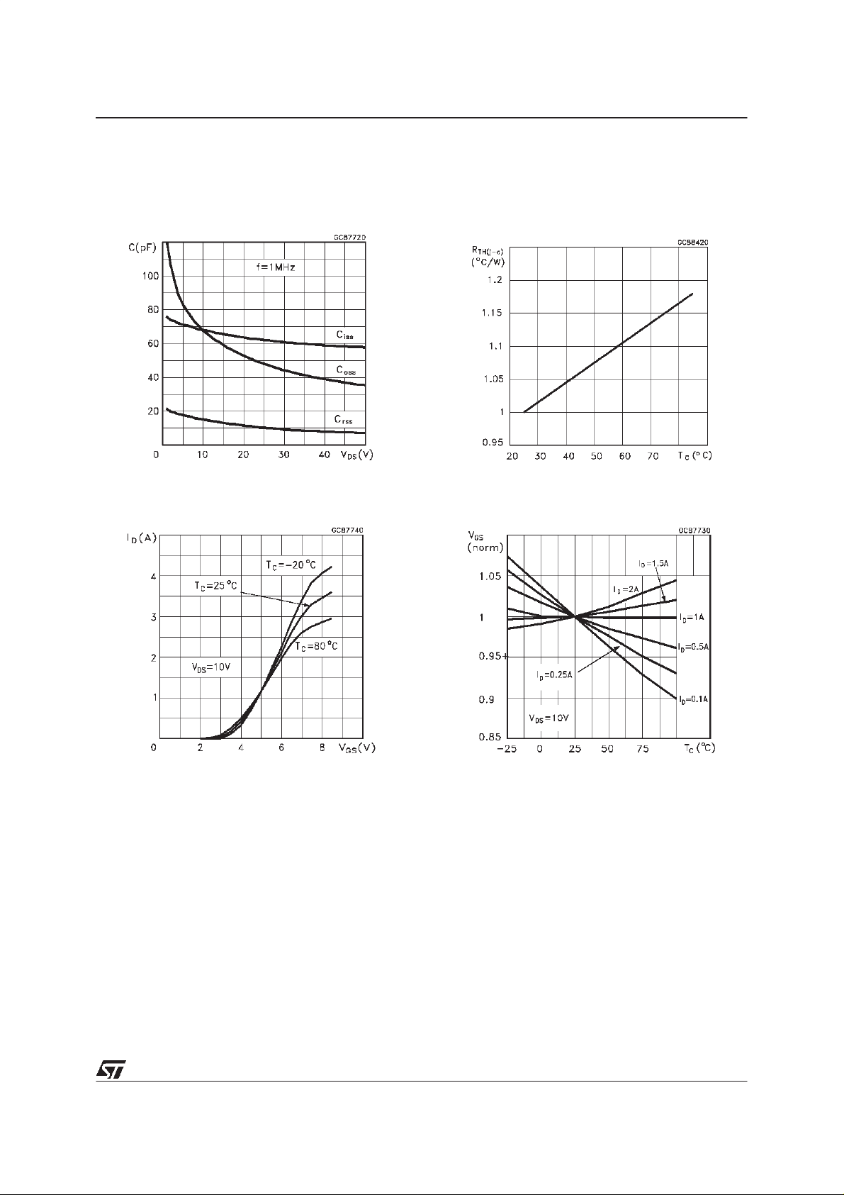
TYPICALPERFORMANCE
SD2918
Capacitancevs Drain-SourceVoltage
Drain Current vs Gate Voltage
Maximum ThermalResistancevs Case
Temperature
Gate-SourceVoltagesvs Case Temperature
3/8
Page 4

SD2918
TYPICALPERFORMANCE
OutputPowervs Input Power OutputPower vs InputPower
OutputPowervs VoltageSupply OutputPower vs GateVoltage
PowerGain& Efficiencyvs OutputPower
4/8
Page 5

30 MHz Test Circuit Schematic
SD2918
RF
INPUT
30 MHz Test Circuit ComponentPart List
V
B
+
+50V
+
RF
OUTPUT
REF. 7143542A
5/8
Page 6

SD2918
30 MHz Test Circuit Photomaster
30 MHz ProductionTest Fixture
REF. 7143542A
6/8
Page 7

M113 (.380 DIA 4/L N/HERM W/FLG) MECHANICALDATA
SD2918
DIM.
MIN. TYP. MAX. MIN. TYP. MAX.
A 5.59 5.84 0.220 0.230
B 19.81 20.83 0.780 0.820
C 18.29 18.54 0.720 0.730
D 24.64 24.89 0.970 0.980
E 9.40 9.78 0.370 0.385
F 0.10 0.15 0.004 0.006
G 2.16 2.67 0.085 0.105
H 4.06 4.57 0.160 0.180
I 7.14 0.281
J 6.22 6.48 0.245 0.255
K 3.05 3.30 0.120 0.130
mm inch
ControllingDimension:Inches
1010936D
7/8
Page 8

SD2918
Information furnished isbelieved tobe accurate and reliable. However, STMicroelectronics assumes noresponsibility for the consequences
of use of such information nor for any infringement of patents or other rights of third parties which may result from its use. No license is
granted by implication or otherwise under any patent or patent rights of STMicroelectronics. Specification mentioned inthis publication are
subject to change without notice. This publication supersedes andreplaces all information previously supplied. STMicroelectronics products
are not authorized for use as critical components inlife support devices or systems without express written approval of STMicroelectronics.
The ST logo is a trademark of STMicroelectronics
1999 STMicroelectronics – Printed in Italy – All Rights Reserved
STMicroelectronicsGROUP OF COMPANIES
Australia - Brazil - China - Finland - France - Germany- Hong Kong - India - Italy - Japan - Malaysia - Malta - Morocco -
Singapore- Spain -Sweden - Switzerland - United Kingdom - U.S.A.
http://www.st.com
.
8/8
 Loading...