

Page 1
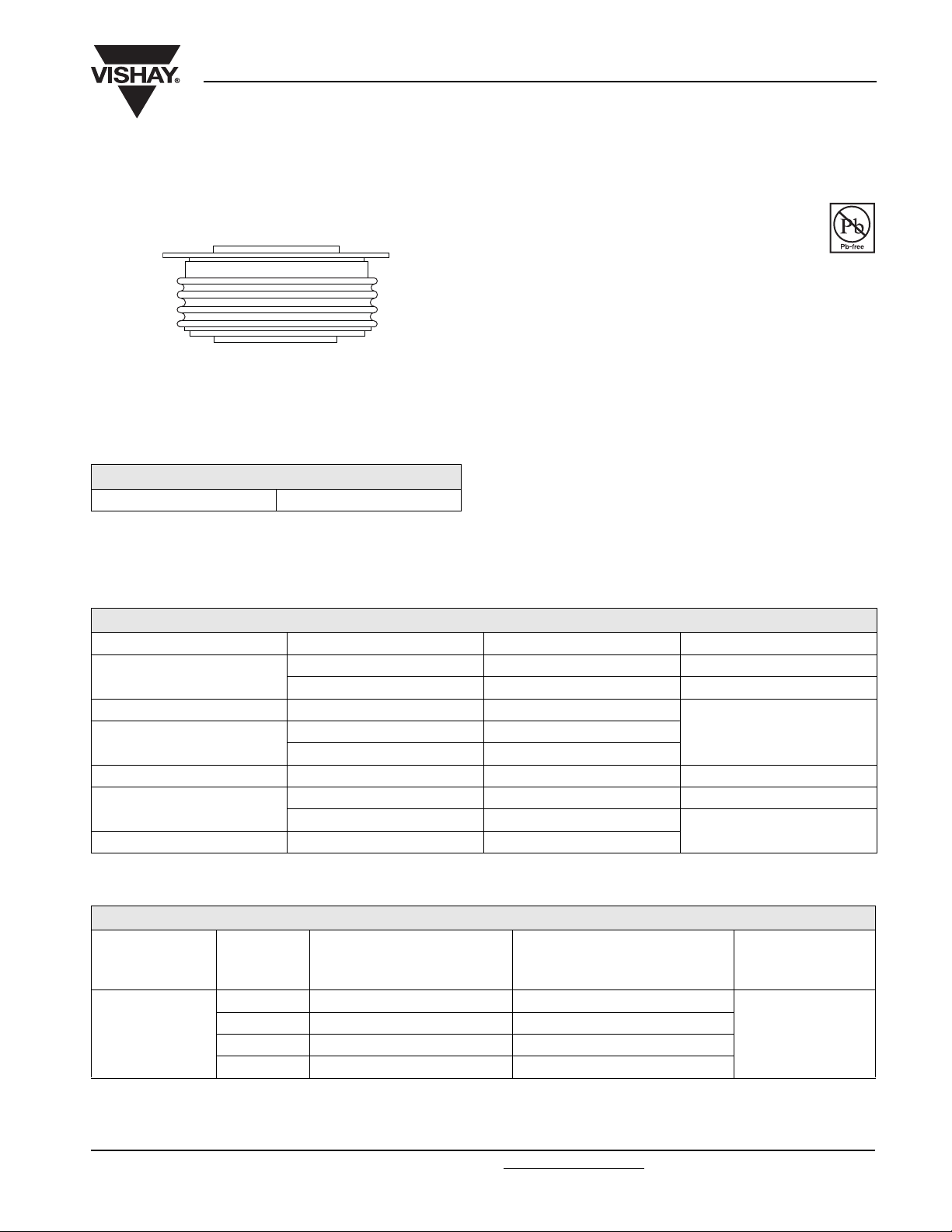
DO-200AB (B-PUK)
PRODUCT SUMMARY
I
F(AV)
SD263C..S50L Series
Vishay High Power Products
Fast Recovery Diodes
(Hockey PUK Version), 375 A
FEATURES
• High power FAST recovery diode series
• 4.5 µs recovery time
• High voltage ratings up to 4500 V
• High current capability
• Optimized turn-on and turn-off characteristics
• Low forward recovery
• Fast and soft reverse recovery
• Press PUK encapsulation
• Case style conform to JEDEC DO-200AB (B-PUK)
• Maximum junction temperature 125 °C
• Lead (Pb)-free
375 A
TYPICAL APPLICATIONS
• Snubber diode for GTO
• High voltage freewheeling diode
• Fast recovery rectifier applications
RoHS
COMPLIANT
MAJOR RATINGS AND CHARACTERISTICS
PARAMETER TEST CONDITIONS VALUES UNITS
I
F(AV)
I
F(RMS)
I
FSM
V
RRM
t
rr
T
J
T
hs
50 Hz 5500
60 Hz 5760
Range 3000 to 4500 V
T
J
375 A
55 °C
408
4.5 µs
125
- 40 to 125
ELECTRICAL SPECIFICATIONS
VOLTAGE RATINGS
V
TYPE NUMBER
SD263C..S50L
, MAXIMUM REPETITIVE
VOLTAGE
CODE
30 3000 3100
36 3600 3700
40 4000 4100
45 4500 4600
RRM
PEAK REVERSE VOLTAGE
V
V
, MAXIMUM NON-REPETITIVE
RSM
PEAK REVERSE VOLTAGE
V
I
AT T
A
°C
MAXIMUM
RRM
= TJ MAXIMUM
J
mA
50
Document Number: 93173 For technical questions, contact: ind-modules@vishay.com
Revision: 14-May-08 1
www.vishay.com
Page 2
SD263C..S50L Series
Vishay High Power Products
Fast Recovery Diodes
(Hockey PUK Version), 375 A
FORWARD CONDUCTION
PARAMETER SYMBOL TEST CONDITIONS VALUES UNITS
Maximum average forward current
at heatsink temperature
Maximum RMS forward current I
Maximum peak, one-cycle forward,
non-repetitive surge current
Maximum I
Maximum I
2
t for fusing I2t
2
√t for fusing I2√t t = 0.1 to 10 ms, no voltage reapplied 1510 kA2√s
Low level value of threshold voltage V
High level value of threshold voltage V
Low level value of forward
slope resistance
High level value of forward
slope resistance
Maximum forward voltage drop V
I
F(AV)
F(RMS)
I
FSM
F(TO)1
F(TO)2
r
f1
r
f2
FM
180° conduction, half sine wave
Double side (single side) cooled
25 °C heatsink temperature double side cooled 725
t = 10 ms
t = 8.3 ms 5760
t = 10 ms
t = 8.3 ms 4850
t = 10 ms
t = 8.3 ms 138
t = 10 ms
t = 8.3 ms 98
(16.7 % x π x I
(I > π x I
(16.7 % x π x I
(I > π x I
No voltage
reapplied
50 % V
RRM
reapplied
No voltage
Sinusoidal half wave,
initial T
= TJ maximum
J
reapplied
50 % V
RRM
reapplied
< I < π x I
F(AV)
), TJ = TJ maximum 1.71
F(AV)
< I < π x I
F(AV)
), TJ = TJ maximum 1.53
F(AV)
), TJ = TJ maximum 1.56
F(AV)
), TJ = TJ maximum 1.64
F(AV)
Ipk = 1000 A, TJ = TJ maximum,
t
= 10 ms sinusoidal wave
p
375 (150) A
55 (85) °C
5500
4630
151
107
3.20 V
A
kA2s
V
mΩ
RECOVERY CHARACTERISTICS
TYPICAL VALUES
AT TJ = 150 °C
AT 25 % I
(µs)
RRM
Q
(µC)
I
FM
rr
I
rr
(A)
t
rr
dir
dt
I
RM(REC)
CODE
MAXIMUM VALUE
= 25 °C
AT T
J
AT 25 % I
t
rr
RRM
(µs)
TEST CONDITIONS
I
pk
SQUARE
PULSE
dI/dt
(A/µs)
(1)
V
t
r
rr
(V)
(A)
S50 5.0 1000 100 - 50 4.5 680 240
Note
(1)
dI/dt = 25 A/µs, TJ = 25 °C
THERMAL AND MECHANICAL SPECIFICATIONS
PARAMETER SYMBOL TEST CONDITIONS VALUES UNITS
Maximum junction operating
temperature range
Maximum storage temperature range T
Maximum thermal resistance,
junction to heatsink
Mounting force, ± 10 % 9800 (1000) N (kg)
Approximate weight 230 g
Case style See dimensions - link at the end of datasheet DO-200AB (B-PUK)
R
T
J
Stg
thJ-hs
- 40 to 125
- 40 to 150
DC operation single side cooled 0.11
DC operation double side cooled 0.05
°C
K/W
t
Q
rr
www.vishay.com For technical questions, contact: ind-modules@vishay.com
Document Number: 93173
2 Revision: 14-May-08
Page 3
SD263C..S50L Series
Fast Recovery Diodes
(Hockey PUK Version), 375 A
ΔR
CONDUCTION ANGLE
Note
• The table above shows the increment of thermal resistance R
CONDUCTION
thJ-hs
SINUSOIDAL CONDUCTION RECTANGULAR CONDUCTION
SINGLE SIDE DOUBLE SIDE SINGLE SIDE DOUBLE SIDE
180° 0.012 0.011 0.008 0.008
120° 0.014 0.015 0.014 0.014
90° 0.018 0.018 0.019 0.019
60° 0.026 0.027 0.027 0.028
30° 0.045 0.046 0.046 0.046
130
120
110
100
90
80
70
60
50
40
30
20
10
050100150200250300
Maximum Allowable Heatsink Temperature (°C)
Average Forward Current (A)
SD263C..S50L Series
(Single Side Cooled)
R (DC) = 0.11 K/W
thJ-hs
Conduction Angle
90°
60°
30°
120°
180°
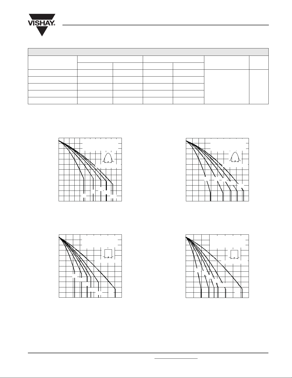
Fig. 1 - Current Ratings Characteristics
Vishay High Power Products
TEST CONDITIONS UNITS
= TJ maximum K/W
T
J
when devices operate at different conduction angles than DC
thJ-hs
130
120
110
100
90
80
70
60
50
40
30
20
10
0 100 200 300 400 500
Maxim um Allowable Heatsink Temperature (°C)
A ver a g e Fo rw a rd C u rre nt (A )
Fig. 3 - Current Ratings Characteristics
SD 2 63C ..S50 L S e ries
(D o uble Side C oo le d )
R (D C ) = 0 .0 5 K /W
th J-hs
Conduction Angle
30°
60°
90°
120°
180°
130
120
110
100
90
80
70
60
50
40
30
20
10
0 50 100 150 200 250 300 350 400 450
Maxim um Allowable Heatsink Tem perature (°C )
SD263C ..S50L Series
(Single Side Cooled)
R ( D C ) = 0 .1 1 K / W
th J-hs
Conduction Period
30°
60°
90°
120°
180°
Average Forw ard Current (A)
Fig. 2 - Current Ratings Characteristics
DC
130
120
110
100
90
80
70
60
50
40
30
20
10
Maximum Allowable Heatsink Temperature (°C)
30°
0200400600800
Average Forward Current (A)
SD263C..S50L Series
(Double Side Cooled)
R (D C) = 0.05 K/W
thJ-h s
Conduction Period
60°
90°
120°
180°
DC
Fig. 4 - Current Ratings Characteristics
Document Number: 93173 For technical questions, contact: ind-modules@vishay.com
www.vishay.com
Revision: 14-May-08 3
Page 4

SD263C..S50L Series
Vishay High Power Products
1600
1400
1200
1000
Maximum Average Forward Power Loss (W)
2250
2000
1750
1500
1250
1000
Maximum Average Forward Power Loss (W)
180°
120°
90°
60°
30°
800
600
400
200
0
0 100 200 300 400 500
Ave rage Fo rwa rd C urre nt (A)
RMS Limit
Con duc tion An gle
SD263C..S50L Series
T = 125°C
J
Fig. 5 - Forward Power Loss Characteristics
DC
180°
120°
90°
60°
30°
RMS Limit
750
500
250
0
0 100 2 00 3 00 400 50 0 60 0 700 80 0
Average Forw ard Current (A)
Conduction Period
SD 26 3C ..S50L Se rie s
T = 125°C
J
Fig. 6 - Forward Power Loss Characteristics
Fast Recovery Diodes
(Hockey PUK Version), 375 A
6000
5000
4000
3000
2000
Peak Half Sin e Wave Forward Current (A)
1000
Fig. 8 - Maximum Non-Repetitive Surge Current
10000
1000
Instantaneous Forw ard Current (A)
100
Fig. 9 - Forward Voltage Drop Characteristics
Ma ximu m No n R e pe tit ive Su rg e C u rre nt
SD 26 3C ..S50L Se ries
0.01 0.1 1
Versus Pulse Train Duration.
50% Rated V Re applie d
Pulse Train Duration (s)
Initial T = 1 25°C
N o V o lt a g e R e a pp l ie d
RRM
J
Single and Double Side Cooled
T = 25°C
J
T = 125°C
J
SD263C..S50L Se ries
12345678
Instantaneous Forw ard Voltage (V)
5500
At Any Rated Load Condition And W ith
50 % R a te d V Ap p lied F ollo w ing Su rg e
5000
4500
4000
3500
3000
2500
2000
1500
SD263C..S50L Series
Pe a k Ha lf Sine W a ve Fo rw a rd C u rre nt (A)
1000
Number Of Equal Amplitude Half Cycle Curren t Pulses (N)
RRM
Init ial T = 1 25 °C
J
@ 60 Hz 0.0083 s
@ 50 Hz 0.0100 s
Fig. 7 - Maximum Non-Repetitive Surge Current
001011
1
Steady State V alue
R = 0.11 K/W
th J-hs
(Single Side Coo le d )
R = 0.05 K/W
th J -h s
Tra nsien t Th erm a l Im pedan ce Z (K/ W )
Fig. 10 - Thermal Impedance Z
th J-hs
0.1
(D ouble Side Cooled)
(D C O p e ra tion)
0.01
SD 263C ..S50L Series
0.001
0.00 1 0.01 0 .1 1 10
Sq ua re W a ve Pulse D uratio n (s)
thJ-hs
Characteristic
Single and Double Side Cooled
www.vishay.com For technical questions, contact: ind-modules@vishay.com
Document Number: 93173
4 Revision: 14-May-08
Page 5

SD263C..S50L Series
Fast Recovery Diodes
(Hockey PUK Version), 375 A
500
450
400
350
300
250
200
150
Fo rw a rd R ec ov ery (V )
100
50
9
SD 263C ..S50L Se ries
8
T = 125 °C; V > 100V
J
7
6
5
4
3
Maximum Reverse Recovery Time - Trr (µs)
2
10 100 1000
Rate Of Fall Of Forward Current - di/dt (A/µs)
Fig. 12 - Recovery Time Characteristics
V
FP
0
0 200 400 6 00 80 0 1 00 0 120 0 1400 1600 18 00 20 00
Fig. 11 - Typical Forward Recovery Characteristics
r
I = 1 0 0 0 A
FM
Sin e Pu lse
500 A
150 A
I
T = 125°C
J
SD263C ..S50L Series
Rate O f Rise Of Fo rwa rd Current - di/dt (A /us)
Vishay High Power Products
T = 25°C
J
600
500
400
300
200
100
0
M a ximu m Re verse R e c ove ry C urre n t - Irr (A)
Rate Of Fall Of Forward Current - di/dt (A/µs)
Fig. 14 - Recovery Current Characteristics
I = 1000 A
FM
Sine Pu lse
500 A
150 A
SD 263C ..S50L S eries
T = 125 °C ; V > 100V
J
r
0 50 100 15 0 20 0 2 50 3 0 0
1400
1200
1000
I = 1000 A
FM
Sine Pulse
500 A
800
600
150 A
400
200
0
Maximum Reverse Recovery Charge - Qrr (µC)
R ate O f Fall Of Fo rwa rd Cur rent - d i/dt (A/µs )
SD 263 C..S50 L Se ries
T = 1 25 °C ; V > 100V
J
r
0 50 100 150 200 250 300
Fig. 13 - Recovery Charge Characteristics
1E4
10 jo ules per pulse
6
4
2
1
1E3
Peak Forward C urre nt (A)
1E2
1E1 1E2 1E3 1E4
0.5
0.3
SD263C..S50L Series
Sinu soida l Pulse
T = 125°C, V = 1500V
J
tp
dv/dt = 1000V/µs
RRM
Pul se B a sew idt h (µs )
Fig. 15 - Maximum Total Energy Loss Per Pulse Characteristics
Document Number: 93173 For technical questions, contact: ind-modules@vishay.com
www.vishay.com
Revision: 14-May-08 5
Page 6

SD263C..S50L Series
Vishay High Power Products
1E4
200
400
1000
1500
1E3
Peak Forward Current (A)
1E2
1E1 1 E2 1 E3 1E4
1E4
1E3
Peak Forward Current (A)
1E2
1E1 1E2 1 E3 1E4
Fig. 17 - Maximum Total Energy Loss
2000
3000
4000
6000
10000
SD263C..S50L Series
Sinu soid al Pulse
T = 55°C , V = 1500V
C
tp
dv/dt = 1000V/u s
RR M
Pulse Basew idth (µs)
Fig. 16 - Frequency Characteristics
SD2 63C ..S50L Se ries
Trapezoid al P uls e
T = 125°C , V = 1500V
J
dv/dt = 1000V/µs
tp
di/dt = 300A/µs
10 jo ules per pulse
6
4
2
1
0.5
0.3
Pulse Basewidth (µs)
Per Pulse Characteristics
Fast Recovery Diodes
(Hockey PUK Version), 375 A
1E4
100
50 Hz
1E3
Peak Forward Current (A)
1E2
1E1 1E2 1E3 1E4
1E4
RRM
1E3
Peak Forward Current (A)
1E2
1E1 1E2 1 E3 1E4
200
400
600
1000
1500
200 0
3000
4000
SD263C..S50L Series
Tra p ezo ida l Pu lse
T = 5 5°C, V = 15 00 V
C
dv/dt = 1000V/us,
di/dt = 300A/us
Pulse B ase width (µs)
Fig. 18 - Frequency Characteristics
SD263C..S50L S eries
Tra pe zoid al P u lse
T = 125°C, V = 1500V
J
dv/d t = 1000V/µ s
di/dt = 100A /µs
RRM
10 joules per pulse
6
4
2
1
0.5
0.3
Pulse Basewidth (µs)
Fig. 19 - Maximum Total Energy Loss
Per Pulse Characteristics
100
tp
50 H z
RRM
tp
1E4
tp
50 H z
100
200
1E3
1500
2000
Peak Forward Current (A)
1E2
1E1 1E2 1E3 1E4
3000
4000
6000
1000
600
400
SD263C..S50L Series
Trap ezoidal Pulse
T = 55°C, V = 1500V
dv/dt = 1000V/us,
di/dt = 100A/us
RRM
C
Pulse Basew idth (µs)
Fig. 20 - Frequency Characteristics
www.vishay.com For technical questions, contact: ind-modules@vishay.com
Document Number: 93173
6 Revision: 14-May-08
Page 7

SD263C..S50L Series
(Hockey PUK Version), 375 A
ORDERING INFORMATION TABLE
Device code
SD 26 3 C 45 S50 L
1
- Diode
2
- Essential part number
3
- 3 = Fast recovery
4
- C = Ceramic PUK
5
- Voltage code x 100 = V
6
-trr code
7
- L = PUK case DO-200AB (B-PUK)
Fast Recovery Diodes
51324
RRM
Vishay High Power Products
67
(see Voltage Ratings table)
Document Number: 93173 For technical questions, contact: ind-modules@vishay.com
Revision: 14-May-08 7
www.vishay.com
Page 8

DIMENSIONS in millimeters (inches)
3.5 (0.14) DIA. NOM. x
1.8 (0.07) deep MIN. both ends
Outline Dimensions
Vishay High Power Products
DO-200AB (B-PUK)
58.5 (2.30) DIA. MAX.
0.8 (0.03)
both ends
25.4 (1)
26.9 (1.06)
Quote between upper and lower pole pieces has to be considered after
application of mounting force (see Thermal and Mechanical Specifications)
34 (1.34) DIA. MAX.
2 places
53 (2.09) DIA. MAX.
Document Number: 95246 For technical questions concerning discrete products, contact: diodes-tech@vishay.com
Revision: 05-Nov-07 For technical questions concerning module products, contact: ind-modules@vishay.com
www.vishay.com
1
Page 9

Legal Disclaimer Notice
Vishay
Notice
The products described herein were acquired by Vishay Intertechnology, Inc., as part of its acquisition of
International Rectifier’s Power Control Systems (PCS) business, which closed in April 2007. Specifications of the
products displayed herein are pending review by Vishay and are subject to the terms and conditions shown below.
Specifications of the products displayed herein are subject to change without notice. Vishay Intertechnology, Inc., or
anyone on its behalf, assumes no responsibility or liability for any errors or inaccuracies.
Information contained herein is intended to provide a product description only. No license, express or implied, by
estoppel or otherwise, to any intellectual property rights is granted by this document. Except as provided in Vishay's
terms and conditions of sale for such products, Vishay assumes no liability whatsoever, and disclaims any express
or implied warranty, relating to sale and/or use of Vishay products including liability or warranties relating to fitness
for a particular purpose, merchantability, or infringement of any patent, copyright, or other intellectual property right.
The products shown herein are not designed for use in medical, life-saving, or life-sustaining applications.
Customers using or selling these products for use in such applications do so at their own risk and agree to fully
indemnify Vishay for any damages resulting from such improper use or sale.
®
International Rectifier
are registered trademarks of International Rectifier Corporation in the U.S. and other countries. All other product
names noted herein may be trademarks of their respective owners.
, IR®, the IR logo, HEXFET®, HEXSense®, HEXDIP®, DOL®, INTERO®, and POWIRTRAIN
®
Document Number: 99901 www.vishay.com
Revision: 12-Mar-07 1
 Loading...