

Datasheet SD200R16MBV, SD200R16MSV, SD200R16MV, SD200R16PBV, SD200R16PSV Datasheet (International Rectifier)
...Page 1
Features
Wide current range
High voltage ratings up to 2400V
High surge current capabilities
Stud cathode and stud anode version
Standard JEDEC types
Typical Applications
Converters
Power supplies
Machine tool controls
High power drives
Medium traction applications
Major Ratings and Characteristics
I
F(AV)
200 A
@ T
C
110 °C
I
F(RMS)
314 A
I
FSM
@ 50Hz 4700 A
@ 60Hz 4920 A
I2t@
50Hz 110 KA2s
@ 60Hz 101 KA2s
V
RRM
range 400 to 2400 V
T
J
- 40 to 180 °C
Parameters SD200N/R Units
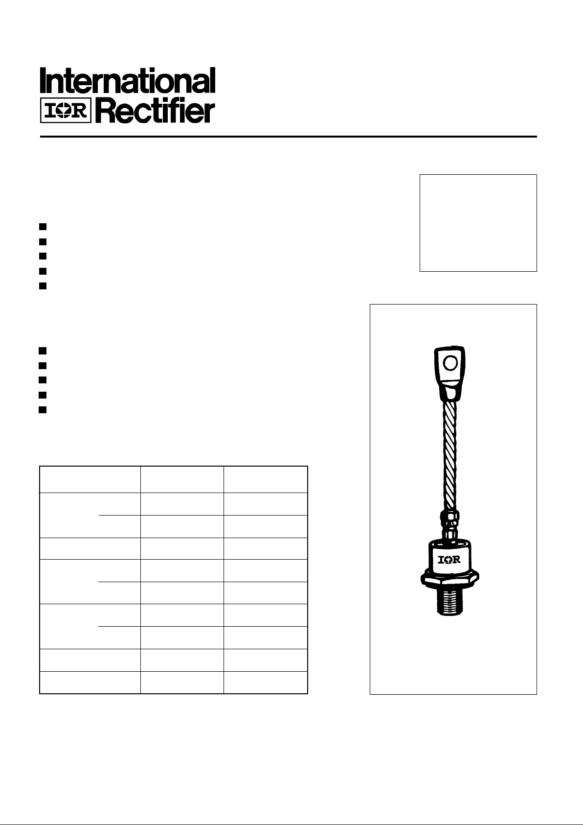
case style
DO-205AC (DO-30)
SD200N/R SERIES
STANDARD RECOVERY DIODES
Stud V ersion
Bulletin I2080/A
200A
Page 2
SD200N/R Series
ELECTRICAL SPECIFICATIONS
Voltage Ratings
Voltage V
RRM
, maximum repetitive V
RSM
, maximum non- I
RRM
max.
Type number Code peak reverse voltage repetitive peak rev. voltage @ T
J
= TJ max.
VVmA
04 400 500
08 800 900
12 1200 1300
16 1600 1700
20 2000 2100
24 2400 2500
SD200N/R 15
I
F(AV)
Max. average forward current 200 A 180° conduction, half sine wave
@ Case temperature 110 °C
I
F(AV)
Max. average forward current 220 A 180° conduction, half sine wave
@ Case temperature 100 °C
I
F(RMS)
Max. RMS forward current 314 A DC @ 95°C case temperature
I
FSM
Max. peak, one-cycle forward, 4700 t = 10ms No voltage
non-repetitive surge current 4920 t = 8.3ms reapplied
3950 t = 10ms 100% V
RRM
4140 t = 8.3ms reapplied Sinusoidal half wave,
I
2
t Maximum I2t for fusing 110 t = 10ms No voltage Initial TJ = TJ max.
101 t = 8.3ms reapplied
78 t = 10ms 100% V
RRM
71 t = 8.3ms rea pplied
I
2
√t Maximum I2√t for fusing 1100 KA2√s t = 0.1 to 10ms, no voltage reapplied
V
F(TO)1
Low level value of threshold
voltage
V
F(TO)2
High level value of threshold
voltage
r
f
1
Low level value of forward
slope resistance
r
f
2
High level value of forward
slope resistance
V
FM
Max. forward voltage drop 1.40 V Ipk= 630A, TJ = TJ max, tp = 10ms sinusoidal wave
Parameter SD200N/R Units Conditions
Forward Conduction
KA2s
A
V
mΩ
0.64 (I > π x I
F(AV)
),TJ = TJ max.
0.79 (16.7% x π x I
F(AV)
< I < π x I
F(AV)
), TJ = TJ max.
1.00 (I > π x I
F(AV)
),TJ = TJ max.
0.90 (16.7% x π x I
F(AV)
< I < π x I
F(AV)
), TJ = TJ max.
Page 3
SD200N/R Series
T
J
Max. junction operating temperature range -40 to 180
T
stg
Max. storage temperature range -55 to 200
R
thJC
Max. thermal resistance, junction to case 0.23 DC operation
R
thCS
Max. thermal resistance, case to heatsink 0.08 Mounting surface, smooth, flat and greased
T Max. allowed mounting torque ±10% 14 Nm Not lubricated threads
wt Approximate weight 120 g
Case style DO-205AC(DO-30) See Outline Table
Parameter SD200N/R Units Conditions
Thermal and Mechanical Specifications
°C
K/W
∆R
thJC
Conduction
(The following table shows the increment of thermal resistence R
thJC
when devices operate at different conduction angles than DC)
180° 0.041 0.030 TJ = TJ max.
120° 0.049 0.051
90° 0.063 0.068
60° 0.093 0.096
30° 0.156 0.157
Conduction angle Sinusoidal conduction Rectangular conduction Units Conditions
K/W
Ordering Information Table
SD 20 0 N 24 P B C
1 2
3
4 5
6
7
Device Code
8
1 - Diode
2 - Essential part number
3 - 0 = Standard recovery
4 - N = Stud Normal Polarity (Cathode to Stud)
R = Stud Reverse Polarity (Anode to Stud)
5 - Voltage code: Code x 100 = V
RRM
(See Voltage Ratings table)
6 - P = Stud base DO-205AC (DO-30) 1/2" 20UNF-2A
M = Stud base DO-205AC (DO-30) M12 X 1.75
7 - B = Flag top terminal (for Cathode/ Anode Leads)
S = Isolated lead with silicone sleeve
(Red = Reverse Polarity; Blue = Normal Polarity)
None = Non isolated lead
8 - C = Ceramic Housing (over 1600V)
V = Glass-metal seal (only up to 1600V)
Page 4

SD200N/R Series
Outline Table
Conforms to JEDEC DO-205AC (DO-30)
All dimensions in millimeters (inches)
GLASS-METAL SEAL
MAX.
21 (0.82)
MAX.
16.5 (0.65)
6.5 (0.26) MIN.
DIA. 8.5 (0.33) NOM.
157 ( 6. 18)
55 (2.16) MIN.
DIA. 23.5 (0.93) MAX.
24 (0.94)
MAX.
SW 27
* FOR METRIC DEVICE: M12 X 1.75
170 (6.69)
1/2"-20UNF-2A*
12.5 (0.49)
MAX.
C.S. 16mm
2.6 (0.10) MAX
2
35 (1.38)
MAX.
(0.015 s.i.)
CERAMIC HOUSING
MAX.
21 (0.82)
MAX.
16.5 (0.65)
6 .5 (0.26 ) MIN.
DIA. 8.5 (0.33) NOM.
55 (2.16) MIN .
DIA. 22.5 (0.88) MAX.
29 (1.14)
MAX.
SW 27
* FOR METRIC DEVICE: M12 X 1.75
157 (6.18)
170 (6.69)
1/2"-20UNF-2A*
12.5 (0.49)
MAX.
C.S. 16mm
2.6 (0.10) MA
X
2
35 (1.38)
MAX.
(0.015 s.i.)
Page 5

SD200N/R Series
Outline Table
DO-205AC (DO-30) Flag
All dimensions in millimeters (inches)
MAX.
GLASS-METAL SEAL
MAX.
21 (0.82)
MAX.
DIA. 23.5 (0.93) MAX.
24 (0.94)
12.5 (0.49)
16.5 (0.65)
5.6 (0.22)
DIA. 5.54 (0.22)
2.4 (0.09)
27 (1.06)
41 (1.61) MAX.
9.5 (0. 37)
*FOR METRIC DEVICE. M12 X 1.75
36.5 (1. 44)
1/2"-20UNF-2A*
CERAMIC HOUSING
MAX.
21 (0.82)
MAX.
DIA. 22.5 (0.88) MAX.
29 (1.14)
MAX.
12 .5 ( 0. 49)
16.5 (0.65)
5.6 (0.22)
DIA. 5.54 (0.22)
2.4 (0.09)
27 (1.06)
40.5 (1.59) MAX.
1/2"-20UNF-2A*
*FOR METRIC DEVICE. M12 X 1.75
9.5 (0. 37)
45 (1.77)
Page 6

SD200N/R Series
Fig. 3 - Forward Power Loss Characteristics
Fig. 2 - Current Ratings Characteristics
Fig. 4 - Forward Power Loss Characteristics
Fig. 1 - Current Ratings Characteristics
90
100
110
120
130
140
150
160
170
180
0 50 100 150 200 250 300 350
DC
30°
60°
90°
120°
180°
Conduction P er i od
Max imum Allowable C ase Te mper a tu r e (° C)
A v erage Forwar d Cu rr en t (A )
SD200N/R Series
R (DC) = 0 .2 3 K /W
thJC
100
110
120
130
140
150
160
170
180
0 40 80 120 160 200 240
30°
60°
90°
120°
180°
Average Fo rward Current ( A)
Conduction Angle
M axim um All owable Case Te m perature (° C)
SD200N/R Series
R (DC) = 0 .2 3 K /W
thJC
20 40 60 80 100 120 140 160 180
M axim um All owable Ambient Tempe rature (° C)
R
=
0
.
0
8
K
/
W
-
D
e
l
t
a
R
t
h
S
A
0
.
3
K
/
W
0
.
4
K
/
W
0
.
2
K
/
W
0
.
1
2
K
/
W
1
.
4
K
/
W
1
.
8
K
/
W
0
.
6
K
/
W
0
.
8
K
/
W
0
50
100
150
200
250
300
350
400
0 50 1 00 150 200 25 0 30 0 350
DC
180°
120°
90°
60°
30°
RMS Limit
Conduction Period
M axim um A verage Fo rward Po wer Loss (W)
Aver age For ward Cur rent ( A)
SD200N/R Series
T = 180°C
J
20 40 60 80 100 120 140 160 180
Max imu m A ll o wabl e Ambi ent Temperatu re (°C)
0
.
3
K
/
W
0
.
4
K
/
W
0
.
2
K
/
W
0
.
1
2
K
/
W
1
.
4
K
/
W
1
.
8
K
/
W
0
.
6
K
/
W
0
.
8
K
/
W
R
=
0
.
0
8
K
/
W
-
D
e
l
t
a
R
t
h
S
A
0
50
100
150
200
250
300
0 50 10 0 150 200 250
180°
120°
90°
60°
30°
RM S Limit
Conduction Angle
Maximum Average Forward P ower Loss (W)
Av e r age For war d Cu r rent (A )
SD20 0N/ R Se rie s
T = 180°C
J
Page 7

SD200N/R Series
Fig. 8 - Thermal Impedance Z
thJC
Characteristic
Fig. 7 - Forward Voltage Drop Characteristics
Fig. 5 - Maximum Non-Repetitive Surge Current Fig. 6 - Maximum Non-Repetitive Surge Current
100
1000
10000
0.5 1 1.5 2 2.5 3 3.5
T = 25°C
J
Instantaneous For ward Voltage (V )
Instantaneous Forward Current (A)
SD20 0N/ R Se rie s
T = 180°C
J
1000
1500
2000
2500
3000
3500
4000
4500
110100
Number Of Equal Amplitude Half Cycle Current Pulses (N)
Peak Half Si ne Wave Forwar d Current (A)
Initial T = 180°C
@ 60 H z 0.00 83 s
@ 50 H z 0.01 00 s
J
SD200N/R Series
At Any Rated Load Condition And With
Rated V Applied Following Su rge.
RRM
1000
1500
2000
2500
3000
3500
4000
4500
5000
0.01 0.1 1
P u lse Train Duration (s )
Peak Hal f Sine Wave For ward Current ( A)
Initial T = 180°C
No Voltage Reappl ied
Rated V Reapplied
RRM
Vers us Puls e Train Duration.
M ax i m um N on Repeti ti v e Sur g e Curr en t
J
SD200N/R Series
0.01
0.1
1
0.001 0.01 0.1 1 10
Square Wave Pulse Du r ation (s )
thJ C
Transient Thermal Impedance Z (K/W)
Steady State Va lue :
R = 0.23 K/W
(D C O perati o n)
thJC
SD200N/ R Series
 Loading...