

Page 1
RF & MICROWAVE TRANSISTORS
.DESIGNED FOR HIGH POWER PULSED
IFF AND DME APPLICATIONS
.600 WATT S (typ .) IFF 10 30/109 0 MHz
.550 WATTS (min.) DME 1025 - 1150 MHz
.5.6 dB MIN. GAIN
.REFRACTORY GOLD METALLIZATI ON
.BALLASTING AND LOW THERMAL
RESISTANCE FOR RELIABILITY AND
RUGGEDNESS
.30:1 LOAD VSWR CAPABILITY AT
SPECIFIED OPERATING CONDITIONS
.INTERNAL INPUT/OUTPUT MATCHED,
COMMON BASE CONFIGURATION
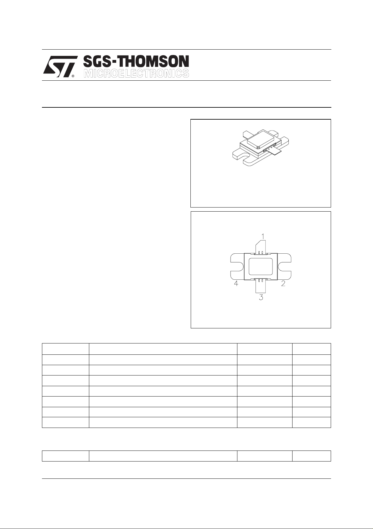
.400 x .500 2LFL (M112)
ORDER CO DE
SD1542
PIN CONNECTION
SD1542
AVIONICS APPLICATIONS
hermetically sealed
BRANDING
SD1542
DESCRIPTION
The SD1542 is a hermetically sealed, gold metallized, silicon NPN power transistor. The
SD1542 is designed for applications req uiring hig h
peak power and low duty cycles such as IFF and
DME. The SD1542 is pa ckaged in a hermetic metal/ceramic package with internal input/output
matching, resulting in improved broadband performance and a low thermal resistance.
ABSOLUTE MAXIMUM RATINGS (T
Symbol Parameter Value Unit
V
V
V
P
T
CBO
CES
EBO
I
C
DISS
T
J
STG
Collector-Base Voltage 65 V
Collector-Emitter Voltage 65 V
Emitter-Base Voltage 3.5 V
Device Current 40 A
Power Dissipation 1350 W
Junction Temperature +200
Storage Temperature
case
= 25°C)
1. Collector 3. Emitter
2. Base 4. Base
65 to +200
−
°
C
°
C
THERMAL DATA
R
TH(j-c)
November 1992
Junction-Case Thermal Resistance 0.06 °C/W
1/4
Page 2
SD1542
ELECTRICAL SPECIFICATIONS (T
case
= 25°C)
STATIC
Symbol Test Condi tions
BV
CBOIC
BV
CESIC
BV
EBOIE
I
CES
h
FE
= 25mA IE = 0mA 65 — — V
= 50mA VBE = 0V 65 — — V
= 10mA IC = 0mA 3.5 — — V
VCE = 50V IE = 0mA — — 35 mA
VCE = 5V IC = .25A 5 — 200 —
DYNAMIC
Symbol Test Conditi ons
P
OUT
G
Note: Pulse Widt h = 10µSec, Duty Cycle = 1%
f = 1025 — 1150MHz PIN = 150 W VCE = 50 V 550 — — W
f = 1025 — 1150MHz PIN = 150 W VCE = 50 V 5.6 — — dB
P
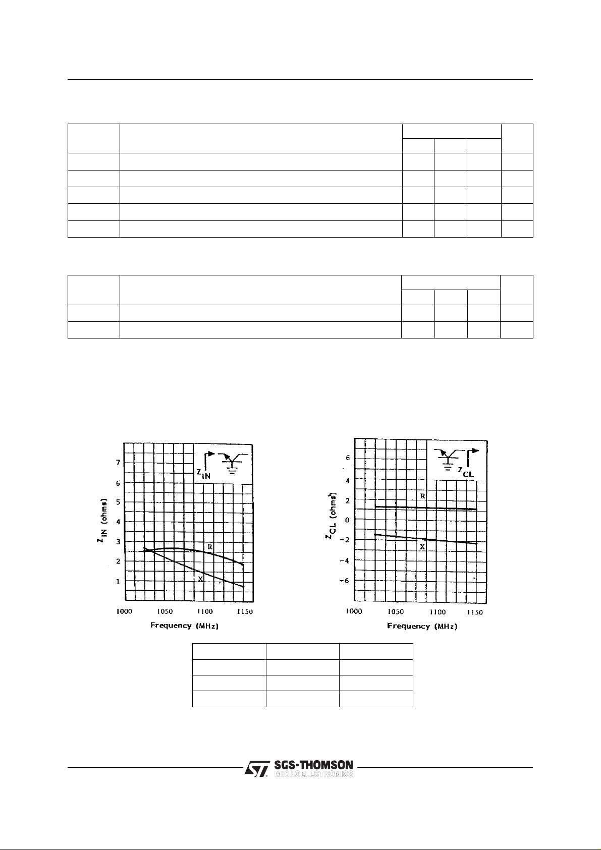
IMPEDANCE DATA
Valu e
Min. Typ. Max.
Value
Min. Typ. Max.
Unit
Unit
TYPICAL INPUT IMPEDANCE
FREQ. ZIN (Ω)Z
1020 MHz 1.78 + j 3.0 1.33 − j 2.7
1090 MHz 1.57 + j 2.1 1.64 − j 3.4
1150 MHz 1.55 + j 1.4 1.93 − j 4.0
TYPICAL COLLECTOR LOAD
IMPEDANCE
(Ω)
CL
2/4
PIN = 150 W
VCE = 50 V
Page 3

TEST CIRCUIT
SD1542
All Dimensions are in inches Unless Otherwise Specified
C1 : 0.4 - 2.5pF Johanson Gigatrim
C2, C3,
C4 : 0.6 - 4.5pF Johanson Gigatrim
C5 : 82pF Chip Capacitor, .055 Sq.
C6 : Pair of 820pF Chip Capacitors, .11 Sq.
C7 : 1000µF Electrolytic
L1 : Loop, #18 Tinned, .36 Wide x .27 Above Circuit
L2 : 4 3/4 Turns, #24 Enameled, Close
Wound, .075 I.D.
PC BOARD LAYOUT
Z1 : 50Ω (.02 Wide)
Z2 : .250 x .120
Z3 : 50Ω, .020 x .330; C1 Tapped .15 From Load
Z4 : .145 x .920
Z5 : .325 x .180
Z6 : .730 x .315
Z7 : .710 x .425 with .140 x .150 Cutout
Z8 : .035 x .780; C4 Tapped .36 from Center
Z9 : 50Ω (.02 Wide)
C1, C4 : Cold End Terminated Through Eyelet
3/4
Page 4

SD1542
PACKAGE MECHANICAL DATA
Ref.: Dwg. No.12-0112
Information furnished is believed to be accurate and reliable. However, SGS-THOMSON Microelectronics assumes no responsability for the
consequences of use of such information nor for any infringement of patents or other rights of third parties which may results from its use. No
license is granted by implication or otherwise under any patent or patent rights of SGS-THOMSON Microelectronics. Specifications mentioned
in this publication are subject to change without notice. This publication supersedes and replaces all information previously supplied.
SGS-THOMSON Microelectronics products are not authorized for use as critical components in life support devices or systems without express
written approval of SGS-THOMSON Microelectonics.
© 1994 SGS-THOMSON Microelectronics - All Rights Reserved
Australia - Brazil - France - Germany - Hong Kong - Italy - Japan - Korea - Malaysia - Malta - Morocco - The Netherlands -
Singapore - Spain - Sweden - Switzerland - Taiwan - Thailand - United Kingdom - U.S.A
SGS-THOMSON Microelectronics GROUP OF COMPANIES
4/4
 Loading...