

Page 1
RF & MICROWAVE TRANSISTORS
.DESIGNED FOR HIGH PO WER PULSED
IFF, DME, TACAN APPLICATIONS
.350 WATTS (typ.) IFF 1030 - 1090 MHz
.300 WATTS (min.) DME 1025 - 1150 M Hz
. 290 WATTS (typ.) TACAN 960 - 1215 MHz
.6.3 dB MIN. GAIN
.REFRACTORY GOLD METALLIZATION
.EMITTER BALLASTING AND LOW
THERMAL RESISTANCE FOR
RELIABILITY AND RUGGEDNESS
.20:1 LOAD VSWR CAPABILITY AT
SPECIFIED OPERATING C ON D I TI ONS
. I NPUT/OUTPUT MATCHED, COMMON
BASE CONFIGURATION
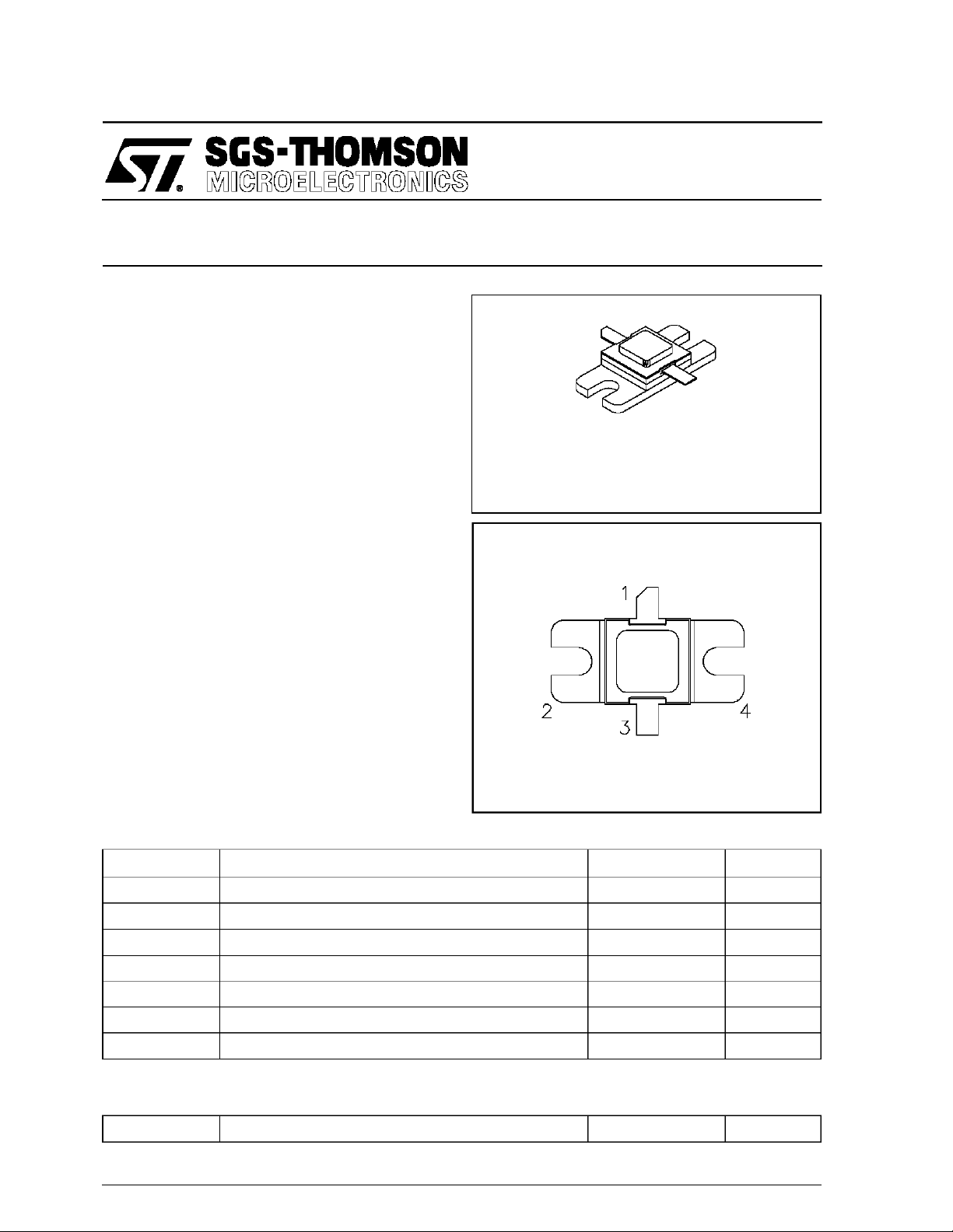
SD1540-08
AVIONI CS APPLICA TIONS
.400 x .400. 2LF L (M138 )
hermetically sealed
ORDER CODE
SD1540-08
PIN CONNECTION
BRANDING
SD1540-8
DESC RIPTIO N
The SD1540-08 is a gold metallized silicon, NPN
power transistordesignedfor applications requiring
high peak power and low duty cycles such as
IFF, DME and TACAN. The SD1540 is packaged
in a metal/ceramic package with internal input/output matching resulting in improved broadband performance and a low thermal resistance.
ABSOLUTE MAXIMUM RATINGS (T
Symbol Parameter Value Uni t
V
CBO
V
CES
V
EBO
I
C
P
DISS
T
J
T
STG
THERMA L DA TA
R
TH(j-c)
Collector-Base Voltage 65 V
Collector-Emitter Voltage 65 V
Emitter-Base Voltage 3.5 V
Device Current 22 A
Power Dissipation 875 W
Junction Temperature +200
Storage Temperature
Junction-Case Thermal Resistance 0.20 °C/W
case
= 25°C)
1. Collector 3. Emitter
2. Base 4. Base
65 to +150
−
°
C
°
C
November 1992
1/5
Page 2
SD1540-08
ELECTRICAL SPECIFICA TIONS (T
case
= 25°C)
STATIC
Symbol Test Conditions
BV
BV
BV
I
CES
h
CBO
CES
EBO
FE
IC= 10mA IE= 0mA 65 — — V
IC= 25mA VBE= 0V 65 — — V
IE= 5mA IC= 0mA 3.5 — — V
VCE= 50V IE= 0mA — — 25 mA
VCE= 5V IC= 1A 10 — — —
DYNAMIC
Symbol Test Conditi ons
P
OUT
G
P
η
C
Note: Pulse Width
f = 1025 — 1150MHz PIN= 70 W VCE= 50 V 300 — — W
f = 1025 — 1150MHz PIN= 70 W VCE= 50 V 6.3 — — dB
f = 1025 — 1150MHz PIN= 70 W VCE= 50 V 35 — — %
10µSec, Duty Cycle = 1%
=
This device i s suitable for use under othe r puls e width/du ty cycle conditions .
Please cont ac t the factory for specific applications a ss istance.
Value
Min. Typ. Max.
Value
Min. Typ. Max.
Unit
Unit
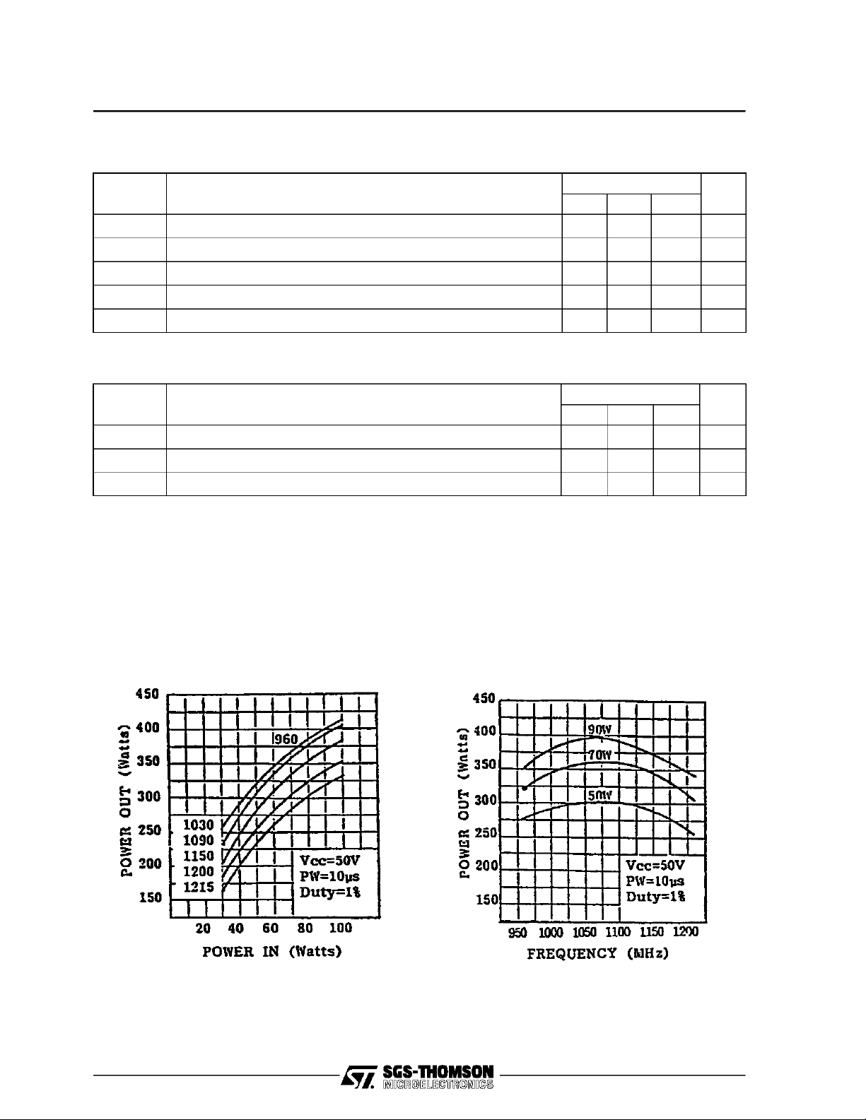
TYPICA L PERFO R MA NCE
POWER OUTPUT vs POWER INPUT POWER OUTPUT vs FREQUENCY
2/5
Page 3

TYPICAL PERFO RM AN CE (cont ’d )
SD 1540-08
EFFICIENCY vs POWER INPUT
IMPEDA NCE DATA
EFFICIENCY vs F REQUENCY
TYPICAL INPUT IMPEDANCE
TYPICAL COLLECTOR LOAD
IMPEDANCE
3/5
Page 4

SD1540-08
TEST CIRCUIT
All Dimension are in Inches
C1,C2.
C3, C4 : .6 - 4.5pF JOHANSON Gigatrim
C5 : 1000µF, 63V, Electrolytic
C6 : 100pF Chip Capacitor Across .090 Gap
L1 : 2 Turns #24 .12 I.D., Spaced Wire Diameter
L2 : 4 Turns #24, .07 I.D., Spaced Wire Diameter
4/5
Z1 : .404 x .075
Z2 : .263 x .995
Z3 : .483 x .077
Z4 : .350 x 1.203
Z5 : .505 x 1.200 with Two Notches .05 Long
Z6 : .335 x .076
Z7 : .260 x .442
Z8 : .310 x .082
By .068 Wide
Page 5

PACKAGE MECHANICAL DATA
Ref.: Dwg. No.12-0138
SD 1540-08
Information furnished isbelieved to be accurate and reliable. However, SGS-THOMSON Microelectronicsassumes no responsability forthe
consequences of use of suchinformation nor for any infringementof patents orother rights of third parties which mayresults from its use. No
license isgrantedby implicationor otherwiseunderany patentor patentrights ofSGS-THOMSON Microelectronics.Specificationsmentioned
in this publicationare subjectto changewithout notice. This publication supersedes andreplaces allinformation previously supplied.
SGS-THOMSON Microelectronicsproductsare notauthorizedforuse ascriticalcomponentsin life supportdevices or systemswithoutexpress
written approvalof SGS-THOMSON Microelectonics.
1994 SGS-THOMSON Microelectronics - All Rights Reserved
Australia - Brazil- France - Germany - Hong Kong- Italy - Japan- Korea - Malaysia- Malta - Morocco- The Netherlands -
Singapore -Spain - Sweden- Switzerland - Taiwan - Thailand - UnitedKingdom - U.S.A
SGS-THOMSON Microelectronics GROUP OF COMPANIES
5/5
 Loading...