

Page 1
RF & MICROWAVE TRANSISTORS
.DESIGNED FOR HIGH PO WER PULSE
IFF, DME, AND TACAN APPLICATIONS
. 2 00 W (t y p.) IFF 1 030 - 1090 MHz
. 150W(min.)DME1025-1150MHz
.140 W (typ. ) TACAN 960 - 1215 MHz
. 7.8 dB MIN. GAIN
.REFRACTORY GOLD METALLIZATION
.BALLASTING AND LOW THERMAL
RESISTANCE FOR RELIABILIT Y AND
RUGGEDNESS
.30:1 LOAD VSWR CAPABILITY AT
SPECIFIED OPERATING CONDI TI ONS
. INPUT AND OUTPUT MATCHED,
COMMON BASE CONFIGURATION
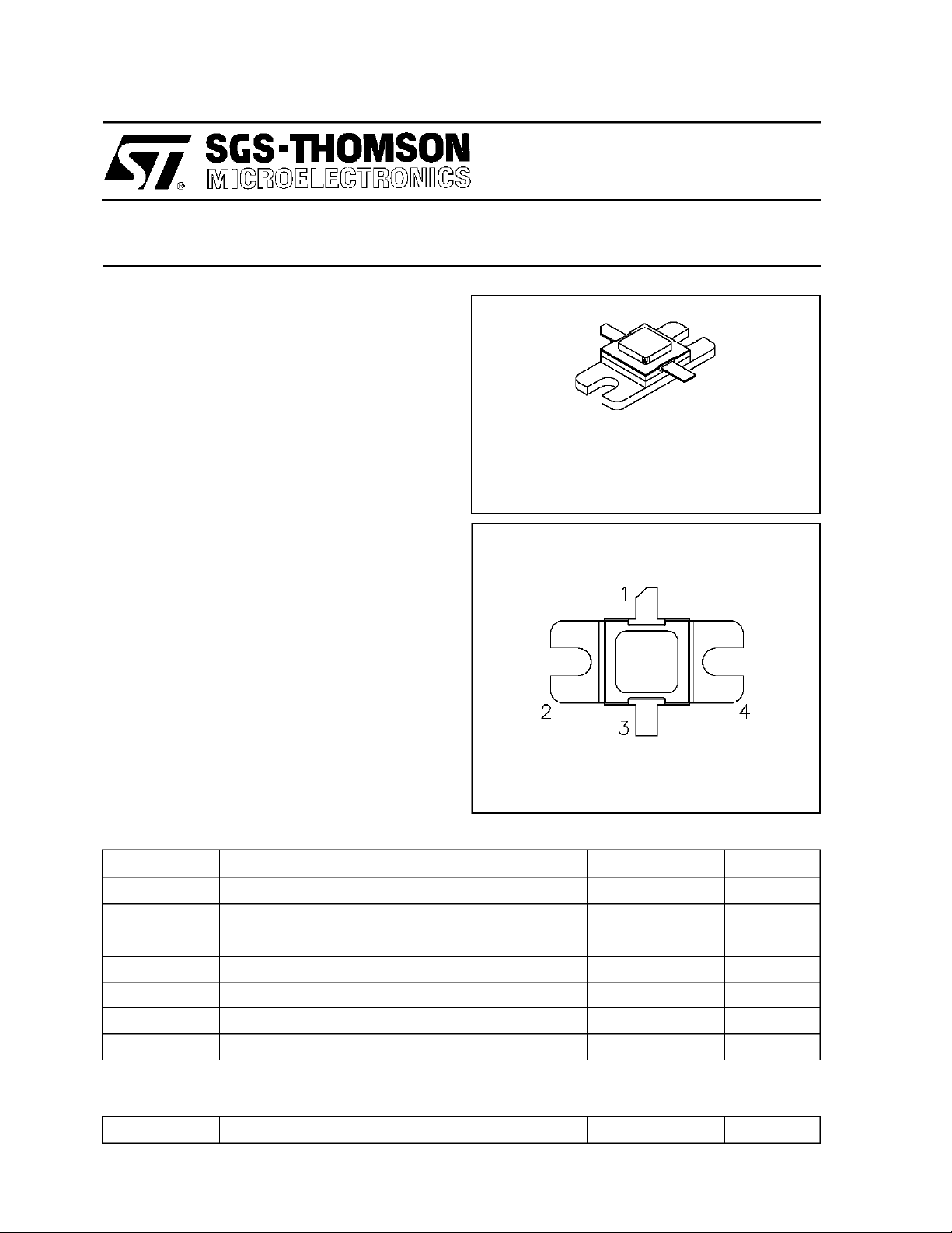
SD1538-08
AVIONI CS APPLICA TIONS
.400 x .400 2LF L (M138)
hermetically sealed
ORDER CODE
SD1538-08
PIN CONNECTION
BRANDING
1538-8
DESC RIPT ION
The SD1538-08 is a gold metallized, silicon NPN
power transistor. The SD1538-08 is designed for
applications requiring high peak power and low
duty cycles such as IFF, DME and TACAN. The
SD1538-08 is packaged in a metal/ceramic package with internal input/output matching, resulting
in improved broadband performance and low thermal resistance.
ABSOLUTE MAXIMUM RATINGS (T
Symbol Parameter Value Uni t
V
V
V
P
T
CBO
CES
EBO
I
C
DISS
T
J
STG
Collector-Base Voltage 65 V
Collector-Emitter Voltage 65 V
Emitter-Base Voltage 3.5 V
Device Current 11 A
Power Dissipation 583 W
Junction Temperature +200
Storage Temperature
case
= 25°C)
1. Collector 3. Emitter
2. Base 4. Base
65 to +150
−
°
C
°
C
THERMA L DA TA
R
TH(j-c)
September 6, 1994
Junction-Case Thermal Resistance 0.30 °C/W
1/5
Page 2
SD1538-08
ELECTRICAL SPECIFICA TIONS (T
case
= 25°C)
STATIC
Symbol Test Conditions
BV
CBOIC
BV
CESIC
BV
EBOIE
I
CES
h
FE
= 10mA IE= 0mA 65 — — V
= 25mA VBE= 0V 65 — — V
= 5mA IC= 0mA 3.5 — — V
VCE= 50V IE= 0mA — — 10 mA
VCE= 5V IC= 300mA 5 — — —
DYNAMIC
Symbol Test Cond iti ons
P
OUT
P
Note: Pulse Width= 10µSec, Duty Cyle= 1%
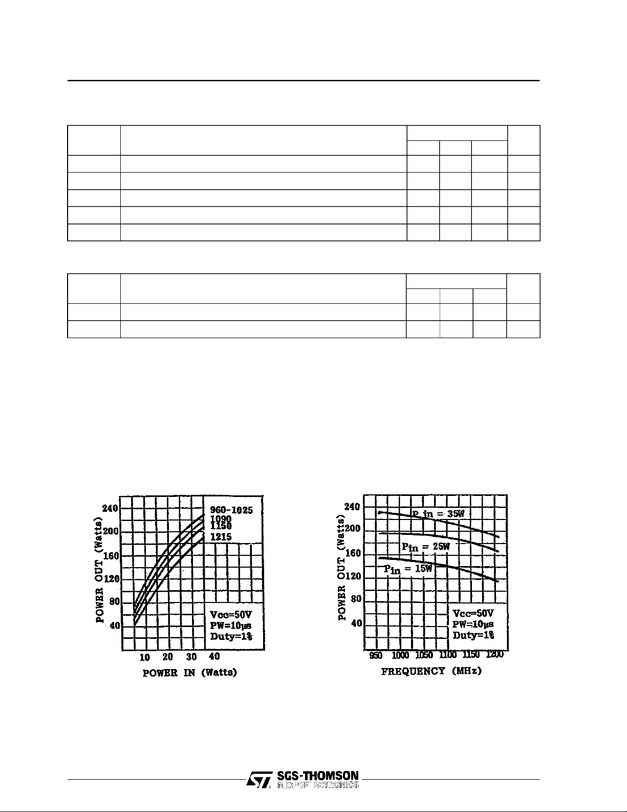
f = 1025 − 1150 MHz PIN= 25 W VCE= 50 V 150 — — W
f = 1025 − 1150 MHz PIN= 25 W VCE= 50 V 7.8 — — dB
G
TYPICA L PERFO R MA NCE
Value
Min. Typ. Max.
Value
Min. Typ. Max.
Unit
Unit
POWER OUTPUT vs POWER INPUT
POWER OUTPUT vs FREQUENCY
2/5
Page 3

TYPICA L PERFOR MA NCE (cont’ d)
SD 1538-08
EFFICIENCY vs POWER INPUT
IMPEDA NC E D ATA
EFFICIENCY vs FREQUENCY
TYPICAL INPUT IMPEDANCE
TYPICAL COLLECTOR LOAD IMPEDANCE
3/5
Page 4

SD1538-08
TEST CIRCUIT
C1, C2 : .6 - 4.5pF Gigatrim
C3 : .100 x .100 120pF Chip Capacitor
C4 : .100 x .100 470pF Chip Capacitor
C5 : 100µF Electrolytic
L1 : #20 AWG
L2 : 3 Turns, #20 AWG Wound on #32 Drill Bit
Board Material: Telfon Er =2.5, Thickness = .031”
4/5
Page 5

PACKAGE MECHANICAL DATA
Ref.: Dwg. No.12-0138 rev. D
SD 1538-08
Information furnished is believed to be accurate and reliable. However, SGS-THOMSON Microelectronics assumes no responsibility
for the consequences of use of such information nor for any infringement of patents or other rights of third parties which may result
from its use. No license is granted by implication or otherwise under any patent or patent rights of SGS-THOMSON Microelectronics. Specifications mentioned in this publication are subject to change without notice. This publication supersedes and replaces all
information previously supplied. SGS-THOMSON Microelectronics products are not authorized for use as critical components in life
support devices or systems without express written approval of SGS-THOMSON Microelectronics.
1994 SGS-THOMSON Microelectronics - All Rights Reserved
Australia - Brazil - France - Germany - Hong Kong - Italy - Japan - Korea - Malaysia - Malta - Morocco - The Netherlands -
Singapore - Spain - Sweden - Switzerland - Taiwan - Thailand - United Kingdom - U.S.A.
SGS-THOMSON Microelectronics GROUP OF COMPANIES
 Loading...