

Page 1
RF & MICROWAVE T RANSIST ORS
.DESIGNED FOR HIGH POWER PULSED
IFF, DME, TACAN APPLICATIONS
.40 WATTS (typ.) IFF 1030 - 1090 MHz
. 35 W ATTS (m in.) D ME 1025 - 1150 MHz
. 25 WATTS (typ.) TACAN 960 - 1215 MHz
.9.0 dB MIN. GAIN
.REFRACTORY GOLD METALLIZATION
.EMITTER BALLASTING AND LOW
THERMAL RESISTANCE FOR
RELIABILITY AND RUGGEDNESS
.INFINITE LOAD VSWR CAPABILITY AT
SPECIFIED OPERATING CONDITIONS
.IN PUT M ATCHED, COMMON BASE
CONFIGURATION
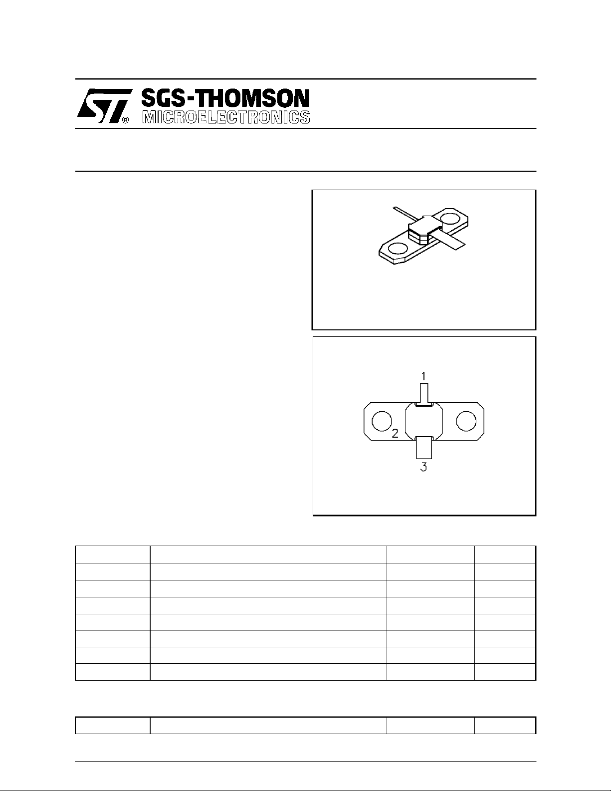
SD1530-08
AVI ONICS APPLICAT IONS
.250 SQ. 2LFL (M105)
hermeticallysealed
ORDER CODE
SD1530-08
PIN CONNECT I ON
BRANDING
1530-8
DESCRIPTI O N
The SD1530-08 is a gold metallized silicon, NPN
power transistor designed forapplications requiring
high peak power and low duty cycles such as
IFF, DME and TACAN. The SD1530-08 is packaged in the .250” input matched hermetic stripline
flange package resulting in improved broadband
performance and a low thermal resistance.
ABSOLUTE MAXIMUM RATINGS (T
Symbol Param eter Value Unit
V
CBO
V
CEO
V
EBO
I
C
P
DISS
T
J
T
STG
THERMAL DATA
R
TH(j-c)
Collector-Base Voltage 65 V
Collector-Emitter Voltage 65 V
Emitter-Base Voltage 3.5 V
Device Current 2.6 A
Power Dissipation 87.5 W
Junction Temperature +200
Storage Temperature
Junction-Case Thermal Resistance 2.0 °C/W
case
= 25°C)
1. Collector 3. Emitter
2. Base
65 to +150
−
°
C
°
C
August 1993
1/5
Page 2
SD1 530-0 8
ELECTRICAL SPECIFICATIONS (T
case
= 25°C)
STATIC
Symbol Test Co nditions
BV
CBOIC
BV
CESIC
BV
EBOIE
I
CES
h
FE
= 10 mA IE= 0mA 65 — — V
= 25 mA VBE= 0 V 65 — — V
= 1mA IC=0mA 3.5 — — V
VCE= 50 V IE= 0mA — — 5 mA
VCE= 5V IC=500 mA 10 — 200
Min. Typ. Max.
Value
DYNAMIC
Symbol Test C onditions
P
OUT
P
η
Note: Pulse W i dth = 10µSec, Duty Cycle = 1%
f = 1025 − 1150 MHz PIN= 5.0 W VCE= 50 V 35 — — W
f = 1025 − 1150 MHz PIN= 5.0 W VCE= 50 V 8.5 — — dB
G
cf=1025 − 1150 MHz PIN= 5.0 W VCE= 50 V 30 — — %
T his dev ice is s uitable for use unde r other pulse width/ duty cycle c onditions.
Please contact the fac tor y for spec ific applic ations assi stance.
Value
Min. Typ. Max.
Unit
Unit
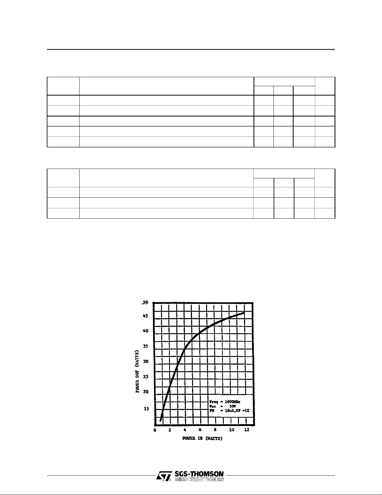
TYPICAL PERFOR MA NCE
POWER OUTPUT vs POWER INPUT
2/5
Page 3

IM PEDANC E DAT A
TYPICAL INPUT IMPEDANCE TYPICAL COLLECTOR LOAD IMPEDANCE
SD1530-08
3/5
Page 4

SD1 530-0 8
TEST CIR CU I T AND PC BOARD L AYOU T
4/5
C1, C3 : 0.6 - 4.5pF, Johanson Gigatrim
C2 : 470pF ATC Chip Capacitor
C4 : 1000pF ATC Chip Capacitor
C5 : 1000µF, 63V, Electrolytic Capacitor
L1 : 4.5 Turns #22 AWG Wire
Z1 : 500mm Line
Z2 : .450” Wire Line Length .600”
Z3 : 50ΩShunt Line
Z4 : .110”x .490”
Z5 : .250”x .700”
Z6 : .250”x .225”
Z7 : Ground
Z8 : .185”x .360”
Z9 : .180”x .120”
Page 5

PACKA GE MECH ANI CA L DATA
Ref.: Dwg. No.12-0105 rev. B
SD1530-08
Information furnished is believed to be accurate and reliable. However, SGS-THOMSON Microelectronics assumes no responsibility
for the consequences of use of such information nor for any infringement of patents or other rights of third parties which may result
from its use. No license is granted by implication or otherwise under any patent or patent rights of SGS-THOMSON Microelectronics. Specifications mentioned in this publication are subject to change without notice. This publication supersedes and replaces all
information previously supplied. SGS-THOMSON Microelectronics products are not authorized for use as critical components in life
support devices or systems without express written approval of SGS-THOMSON Microelectronics.
1994 SGS-THOMSON Microelectronics - All Rights Reserved
Australia - Brazil - France - Germany - Hong Kong - Italy - Japan - Korea - Malaysia - Malta - Morocco - The Netherlands -
Singapore - Spain - Sweden - Switzerland - Taiwan - Thailand - United Kingdom - U.S.A.
SGS-THOMSON Microelectronics GROUP OF COMPANIES
5/5
 Loading...