

Page 1

Super Device Microelectronics Co., Ltd.
SD101B Low Power Receiver IC
Description
The SD101B is a low power receiver IC and it is suitable for use in a
variety of low power radio applications including remote keyless entry. The
SD101B is based on a single-conversion, super-heterodyne receiver
architecture and incorporates an entire phase-locked loop (PLL) for precise
local oscillator generation. In addition, the SD101B provides an RSSI
output.
Features
Extremely low power operation
Low external part count
Receiver input frequency : 290 ~ 460 MHz
On-chip VCO with integrated PLL using crystal oscillator reference
PLL power down feature
Integrated IF and data filters
RSSI output
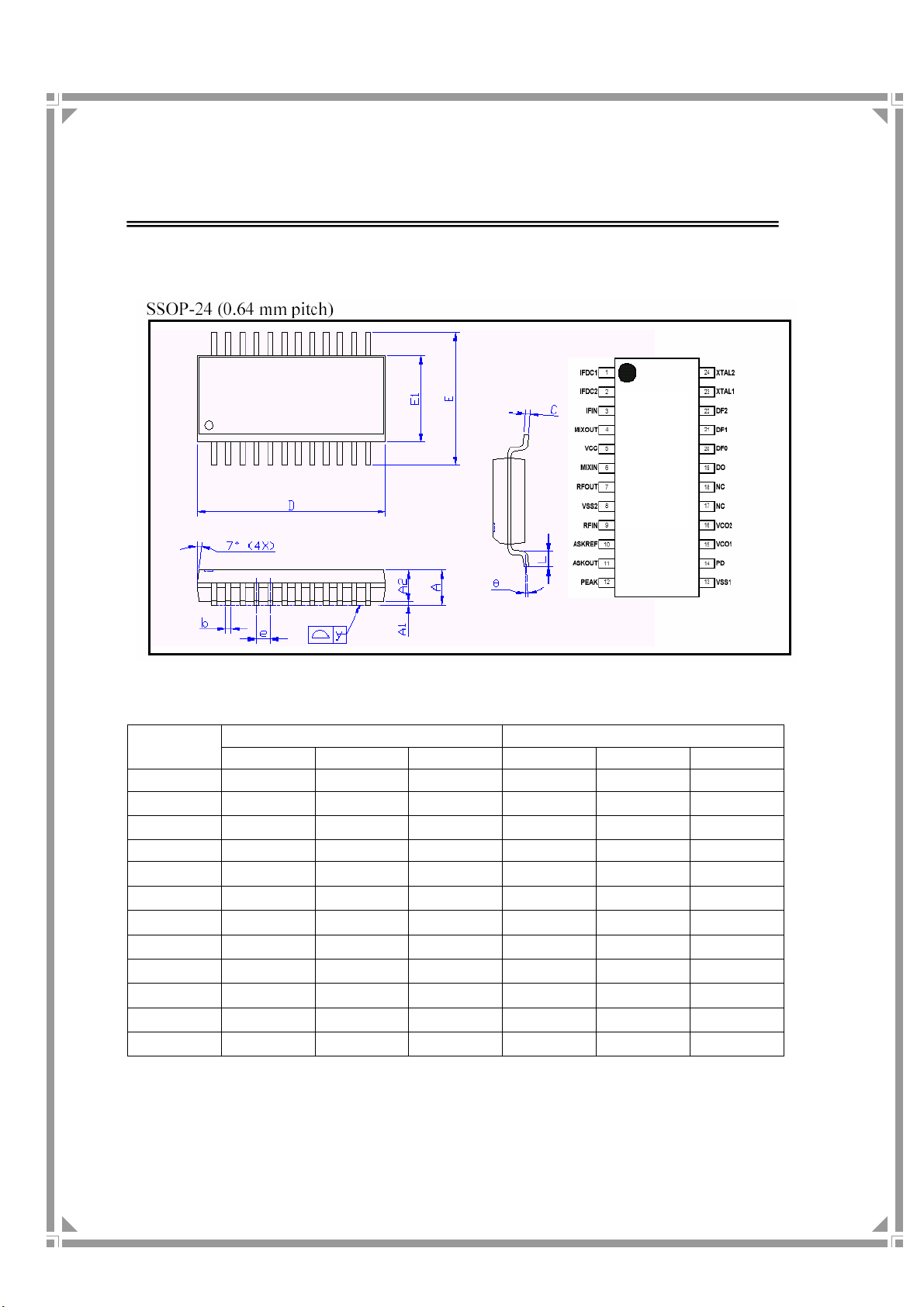
SSOP-24 package (0.64 mm pitch)
Applications
Wireless mouse
Video sender remote controller
Car alarm and home security systems
Functional Description
The SD101B receiver IC incorporates an LNA; mixer; PLL-based local
oscillator including VCO, fixed divider (÷ 64), reference crystal oscillator,
phase-frequency detector (PFD), and charge pump; IF filter; logarithmic
amplifier; data filter; peak detector; and 1bit comparator and is capable of
demodulating ASK input signals.
1 of 5
Page 2
SD101B
Package and Pin Assignment
Super-Devic
SD101B
e
Symbols
Dimensions in mm Dimensions in inch
Min. Nom. Max. Min. Nom. Max.
A 1.35 1.60 1.75 0.053 0.064 0.069
A1 0.10
A2
-
-
1.45
0.25 0.004 0.010
- -
0.057
-
b 0.20 0.25 0.30 0.008 0.010 0.012
C 0.19
D 8.55
E 5.80
E1 3.80
e
-
L 0.40
y
- -
0 00
-
-
-
-
0.64
-
-
0.25 0.007
8.75 0.337
6.20 0.228
4.00 0.150
-
-
1.27 0.016
0.10
0
0
g
- -
0
-
-
-
-
0.025
-
-
0.010
0.344
0.244
0.157
-
0.050
0.004
8
0
2 of 5
Page 3

SD101B
Pin Descriptions
Numbe
Name Description
r
1 IFDC1
2 IFDC2
3 IFIN
MIXO
4
UT
5 VCC
6 MIXIN
RFOU
7
8 VSS2
9 RFIN
ASKR
10
11
EF
ASKO
UT
12 PEAK
If amplifier feedback
decoupling connections
IF amplifier input
Mixer output
Nominal 5V supply
RF mixer input
Open collector LNA
output
T
LNA ground
LNA input
Comparator reference level
Comparator output
Peak detector output
Numbe
Name Description
r
13 VSS1
14 PD
15 VCO1
16 VCO2
17 NC
18 RSS1
19 DO
20 DF0
21 DF1
22 DF2
23 XTAL1
24 XTAL2
Ground
PLL power down: low
Open collector differential
VCO outputs
No connection
RSSI output
Charge pump output
Data filter external
connections
Crystal oscillator external
connections
Absolute Maximum Ratings
VSS = V
Supply voltage
Operating temperature
range
Storage temperature range
Soldering temperature range
Soldering time range
SS1
= V
SS2
Parameter
= 0V
Symb
ol
VCC
T
OPR
T
STG
T
SLD
T
SLD
Rating
VSS-0.5 to VSS
-40 to 85
-55 to 150
Uni
t
O
O
O
V
C
C
C
+8.0
255
10 s
3 of 5
Page 4

SD101B
K
Recommended Operating Conditions
VSS = V
Supply voltage range
RF input frequency
Operating temperature
= 0V
SS2
Parameter Symbol
V
CC
F
RFIN
T
A
min. typ. max.
4.75 5.0 7.0 V
290 460 MHZ
-10 25 60
Value
Unit
O
C
Electrical Characteristics
(VCC= 4.75 to 7.0 V,V
Parameter Symbol Condition
Current consumption
Current consumption(PLL off)
Sensitivitya
Signal handlingb
Integrated IF filter-3-dB low pass
cutoff frequency
Adjacent channel rejectionc
ASK output duty ratio DR 40 50 60 %
Peak detector source current
Peak detector leakage current
Charge pump source/sink
current
PD logic HIGH input voltage
PD logic LOW input voltage
ASKOUT logic HIGH output
voltage
ASKOUT logic LOW output voltage
= OV , TA = -40 to 85 unless otherwise noted)
SS1
Value
typ. max.
2.4 3.0
1.8 2.4
-103
±30
0.5
V
SS2
-0.5
0.7*
V
CC
I
,total V
CC
,noPL
I
CC
L
α
SENS
α
SH
f
,-3dB
IF
α
ACR
I
peak
I
leak
I
CP
V
IL,PD
V
IL,PD
V
OH,ASKO
UT
V
OL,ASKO
UT
min.
= 5V
CC
=5V;VPD=OV
V
CC
f
=434MHz;2
RFIN
B/s
-30
450 550 750 KHz
65 dB
500 µA
250 nA
VCC -
load
load
= 10µA
= 10µA
I
I
Unit
-100
dB
dB
µA
V
+
CC
0.5
V
SS2
-0.5
0.3*
V
CC
m
A
m
A
m
m
V
V
V
V
4 of 5
Page 5

SD101B
Note of Electrical Characteristics
Sensitivity is defined as the minimum average signal level measured at
the input which is necessary to achieve a bit error rate of 0.01 when
the input signal is a return-to-zero (RZ) pulse with an average duty
cycle of 50%. The RF input is assumed to be matched to 50 ohms.
Signal handling is defined as the maximum input signal capable of
being successfully demodulated. It is assumed that the input signal is
ASK modulated with a minimum extinction ratio of 40 dB. The RF
input is assumed to be matched to 50 ohms.
Adjacent channel rejection is defined for an interfering tone αACR [dB]
above the receiving threshold and 10 MHz offset from the carrier giving
a 3dB reduction in sensitivity.
Contact information
For additional information please visit
http://www.super-device.com.tw
Tel: +886-2-8226-1788
Fax: +886-2-8226-2277
e-mail: sd@super-device.com.tw
Data of release:03-2002
~End~
5 of 5
 Loading...