

Page 1

INTEGRATED CIRCUITS
SCC2698B
Enhanced octal universal asynchronous
receiver/transmitter (Octal UART)
Product specification
Supersedes data of 1995 May 01
IC19 Data Handbook
1998 Sep 04
Page 2

Philips Semiconductors Product specification
PACKAGES
DWG #
Enhanced octal universal asynchronous
receiver/transmitter (Octal UART)
DESCRIPTION
The SCC2698B Enhanced Octal Universal Asynchronous
Receiver/Transmitter (Octal UART) is a single chip MOS-LSI
communications device that provides eight full-duplex asynchronous
receiver/transmitter channels in a single package. It is fabricated
with CMOS technology which combines the benefits of high density
and low power consumption.
The operating speed of each receiver and transmitter can be
selected independently as one of eighteen fixed baud rates, a 16X
clock derived from a programmable counter/timer, or an external 1X
or 16X clock. The baud rate generator and counter/timer can
operate directly from a crystal or from external clock inputs. The
ability to independently program the operating speed of the receiver
and transmitter make the Octal UART particularly attractive for
dual-speed channel applications such as clustered terminal
systems.
The receiver is quadruple buffered to minimize the potential of
receiver overrun or to reduce interrupt overhead in interrupt driven
systems. In addition, a handshaking capability is provided to disable
a remote UART transmitter when the receiver buffer is full.
The UART provides a power-down mode in which the oscillator is
frozen but the register contents are stored. This results in reduced
power consumption on the order of several magnitudes. The Octal
UART is fully TTL compatible and operates from a single +5V power
supply.
The SCC2698B is an upwardly compatible version of the 2698A
Octal UART. In PLCC packaging, it is enhanced by the addition of
receiver ready or FIFO full status outputs, and transmitter empty
status outputs for each channel on 16 multipurpose I/O pins. The
multipurpose I/O pins of the SCC2698B were inputs only on the
SCC2698A.
SCC2698B
FEATURES
• Eight full-duplex independent asynchronous receiver/
transmitters
• Quadruple buffered receiver data register
• Programmable data format:
– 5 to 8 data bits plus parity
– Odd, even, no parity or force parity
– 1, 1.5 or 2 stop bits programmable in 1/16-bit incre-
ments
• Baud rate for the receiver and transmitter selectable from:
– 18 fixed rates: 50 to 38.4K baud
Non-standard rates to 1 15.2K baud
– User-defined rates from the programmable counter/tim-
er associated with each of four blocks
– External 1x or 16x clock
• Parity, framing, and overrun error detection
• False start bit detection
• Line break detection and generation
• Programmable channel mode
– Normal (full-duplex), automatic echo, local loop back,
remote loopback
• Four multi-function programmable 16-bit counter/timers
• Four interrupt outputs with eight maskable interrupting
conditions for each output
• Receiver ready/FIFO full and transmitter ready status
available on 16 multi-function pins in PLCC package
• On-chip crystal oscillator
• TTL compatible
• Single +5V power supply with low power mode
• Eight multi-purpose output pins
• Sixteen multi-purpose I/O pins
• Sixteen multi-purpose Input pins with pull-up resistors
ORDERING INFORMATION
COMMERCIAL INDUSTRIAL
VCC = +5V +5%, TA = 0°C to +70°C VCC = +5V +5%, TA = –40°C to +85°C
84-Pin Plastic Leaded Chip Carrier (PLCC) SCC2698BC1A84 SCC2698BE1A84 SOT189-3
NOTE: Pin Grid Array (PGA) package version is available from Philips Components Military Division.
DD
1
PARAMETER RATING UNIT
to GND
2
3
3
2
Note 4
–0.5 to +7.0 V
–0.5 to V
+0.5 V
CC
o
C
o
C
ABSOLUTE MAXIMUM RATINGS
SYMBOL
T
A
T
STG
V
CC
V
S
P
D
NOTES:
1. Stresses above those listed under Absolute Maximum Ratings may cause permanent damage to the device. This is a stress rating only and
functional operation of the device at these or any other condition above those indicated in the operation section of this specification is not
implied.
2. For operating at elevated temperatures, the device must be derated based on +150°C maximum junction temperature.
3. This product includes circuitry specifically designed for the protection of its internal devices from damaging effects of excessive static
charge. Nonetheless, it is suggested that conventional precautions be taken to avoid applying any voltages larger than the rated maxima.
4. Parameters are valid over specified temperature range. See ordering information table for applicable temperature range and operating
supply range.
1998 Sep 04 853-1 127 19974
Operating ambient temperature range
Storage temperature range –65 to +150
Voltage from V
Voltage from any pin to ground
Power dissipation 1 W
Page 3
Philips Semiconductors Product specification
Enhanced octal universal asynchronous
receiver/transmitter (Octal UART)
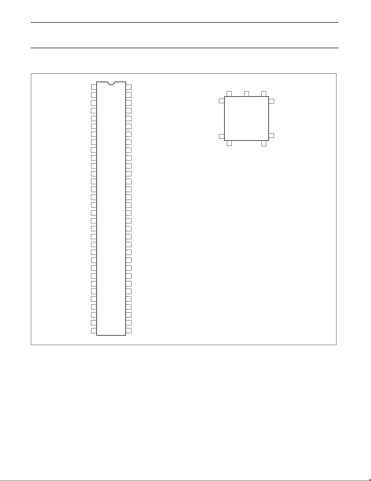
PIN CONFIGURATIONS
RxDa
V
CC
X2
X1/CLK
D0
D1
D2
NC
D3
NC
D4
NC
D5
RESET
D6
D7
CEN
WRN
GND
RDN
A0
A1
A2
A3
A4
A5
MP10a
MP10b
INTRAN
INTRBN
MP10c
MP10d
TxDb
1
2
3
4
5
6
7
8
9
10
11
12
13
14
15
16
17
18
19
20
21
22
23
24
25
26
27
28
29
30
31
32
64
63
62
61
60
59
58
57
56
55
54
53
52
51
50
49
48
47
45
45
44
43
42
41
40
39
38
37
36
35
34
33
TxDa
RxDc
TxDc
RxDe
MP10h
MP10g
RxDg
TxDe
TxDg
MPOa
MPOc
MPOe
MPOg
GND
MP10f
MP10e
RxDh
RxDf
RxDd
RxDb
TxDh
MPOh
Test input
MPOf
TxDf
MPOd
TxDd
INTRDN
INTRCN
V
CC
MPOb
SCC2698B
11
1
75
12
PLCC
32
33
Pin Function Pin Function Pin Function
1
TxDa
2
MPP2g
3
RxDa
4
MPP2h
5
V
CC
X2
6
X1/CLK
7
D0
8
D1
9
D2
10
D3
11
D4
12
D5
13
MPI1a
14
RESET
15
D6
16
D7
17
CEN
18
WRN
19
GND
20
MPI1b
21
RDN
22
A0
23
MPP1a
24
A1
25
MPP1b
26
A2
27
MPP2a
28
29
A3
30
MPP2b
31
A4
32
A5
33
MPI0a
34
MPI0b
35
INTRAN
36
INTRBN
37
MPI0c
38
MPI1c
39
MPI0d
40
MPI1d
41
TxDb
42
MPP1c
43
MPOb
44
MPP1d
45
V
CC
INTRCN
46
INTRDN
47
MPP2c
48
TxDd
49
MPP2d
50
MPOd
51
TxDf
52
MPOf
53
MPOh
54
TxDh
55
RxDb
56
74
54
53
57
RxDd
58
RxDf
59
RxDh
60
MPI1e
61
MPI0e
62
MPI1f
63
MPI0f
64
MPP1e
65
GND
66
MPP1f
67
MPOg
68
MPP2e
69
MPOe
70
MPP2f
71
MPOc
72
MPOa
73
TxDg
74
TxDe
75
RxDg
76
MPI0g
77
MPI0h
78
MPI1g
79
RxDe
80
MPIh
81
TxDc
82
MPP1g
83
RxDc
84
MPP1h
SD00184
1998 Sep 04
Figure 1. Pin Configurations
3
Page 4
Philips Semiconductors Product specification
Enhanced octal universal asynchronous
receiver/transmitter (Octal UART)
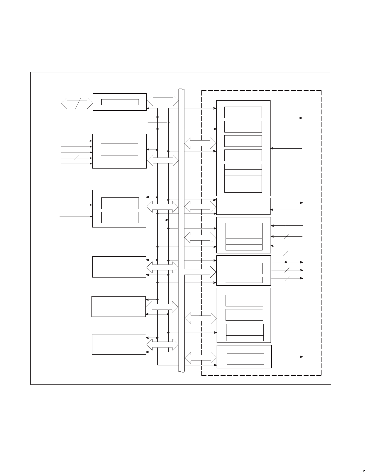
BLOCK DIAGRAM
D0–D7
RDN
WRN
CEN
A0–A5
RESET
X1/CLK
8
6
X2
BUS BUFFER
TIMING
CONTROL
OPERATION CONTROL
ADDRESS
DECODE
R/W CONTROL
TIMING
CRYSTAL
OSCILLATOR
POWER-ON
LOGIC
BLOCK B
(SAME AS A)
INTERNAL DATA
BUS
CHANNEL A
TRANSMIT HOLD
REGISTER
TRANSMIT SHIFT
REGISTER
RECEIVE HOLD
REGISTER (3)
RECEIVE SHIFT
REGISTER
MR1, 2
CR
SR
CSR Rx
CSR Tx
CHANNEL B
(AS ABOVE)
INPUT PORT
CHANGE-OF-
STATE
DETECTORS (4)
IPCR
ACR
OUTPUT PORT
FUNCTION SELECT
LOGIC
OPCR
SCC2698B
BLOCK A
TxDA
RxDA
TxDb
RxDb
4
MPI0
4
MPIb
4
MPP1
4
MPP2
2
MPO
1998 Sep 04
BLOCK C
(SAME AS A)
BLOCK D
(SAME AS A)
Figure 2. Block Diagram
4
TIMING
CLOCK
SELECTORS
COUNTER/
TIMER
ACR
CTUR
CTLR
INTERRUPT CONTROL
IMR
ISR
INTRAN
SD00185
Page 5

Philips Semiconductors Product specification
MNEMONIC
PIN
TYPE
NAME AND FUNCTION
Enhanced octal universal asynchronous
receiver/transmitter (Octal UART)
PIN DESCRIPTION
PIN
NO.
D0–D7 8–13,
CEN 18 I Chip Enable: Active-Low input. When Low, data transfers between the CPU and the Octal UART are
WRN 19 I Write Strobe: Active-Low input. A Low on this pin while CEN is Low causes the contents of the data
RDN 22 I Read Strobe: Active-Low input. A Low on this pin while CEN is Low causes the contents of the
A0–A5 23, 25,
RESET 15 I Reset: Master reset. A High on this pin clears the status register (SR), clears the interrupt mask
INTRAN–
INTRDN
X1/CLK 7 I Crystal 1: Crystal or external clock input. When using the crystal oscillator, this pin serves as the
X2 6 I Crystal 2: Connection for other side of crystal. If an external source is used instead of a crystal, this
RxDa–RxDh 3, 56,
TxDa–TxDh 1, 41,
MPOa–MPOh 72, 43,
MPI0a–MPI0h 33, 34,
16, 17
27, 29,
31, 32
35, 36,
46, 47
83, 57,
79, 58,
75, 59
81, 49,
74, 52,
73, 55
71, 51,
69, 53,
67, 54
37, 39,
61, 63,
76, 77
I/O Data Bus: Active–High 8-bit bidirectional 3-State data bus. Bit 0 is the LSB and bit 7 is the MSB. All
data, command, and status transfers between the CPU and the Octal UART take place over this bus.
The direction of the transfer is controlled by the WRN and RDN inputs when the CEN input is low.
When the CEN input is High, the data bus is in the 3-State condition.
enabled on D0–D7 as controlled by the WRN, RDN and A0–A5 inputs. When CEN is High, the Octal
UART is effectively isolated from the data bus and D0–D7 are placed in the 3-State condition.
bus to be transferred to the register selected by A0–A5. The transfer occurs on the trailing (rising)
edge of the signal.
register selected by A0–A5 to be placed on the data bus. The read cycle begins on the leading
(falling) edge of RDN.
I Address Inputs: Active-High address inputs to select the Octal UART registers for read/write
operations.
register (IMR), clears the interrupt status register (ISR), clears the output port configuration register
(OPCR), places the receiver and transmitter in the inactive state causing the TxD output to go to the
marking (High) state, and stops the counter/timer. Clears power-down mode and interrupts. Clears
Test Modes, sets MR pointer to MR1.
O Interrupt Request: This active-Low open drain output is asserted on occurrence of one or more of
eight maskable interrupting conditions. The CPU can read the interrupt status register to determine
the interrupting condition(s).
connection for one side of the crystal. If a crystal is not used, an external clock is supplied at this
input. An external clock (or crystal) is required even if the internal baud rate generator is not utilized.
This clock is used to drive the internal baud rate generator, as an optional input to the timer/counter,
and to provide other clocking signals required by the chip.
connection should be left open (see Figure 7).
I Receiver Serial Data Input: The least significant bit is received first. If external receiver clock is
specified, this input is sampled on the rising edge of the clock. If internal clock is used, the RxD input
is sampled on the rising edge of the RxC1x signal as seen on the MPO pin.
O Transmitter Serial Data Output: The least significant bit is transmitted first. This output is held in the
marking (High) condition when the transmitter is idle or disabled and when the Octal UART is
operating in local loopback mode. If external transmitter is specified, the data is shifted on the falling
edge of the transmitter clock. If internal clock is used, the TxD output changes on the falling edge of
the TxC1x signal as seen on the MPO pin.
O Multi-Purpose Output: Each of the four DUARTS has two MPO pins (one per UART). One of the
following eight functions can be selected for this output pin by programming the OPCR (output port
configuration register). Note that reset conditions MPO pins to RTSN.
RTSN – Request to send active-Low output. This output is asserted and negated via the command
register. By appropriate programming of the mode registers, (MR1[7])=1 R TSN can be programmed to
be automatically reset after the character in the transmitter is completely shifted or when the receiver
FIFO and shift register are full. RTSN is an internal signal which normally represents the condition of
the receiver FIFO not full, i.e., the receiver can request more data to be sent. However, it can also be
controlled by the transmitter empty and the commands 8h and 9h written to the CR (command
register).
C/TO – The counter/timer output.
TxC1X – The 1X clock for the transmitter.
TxC16X – The 16X clock for the transmitter.
RxC1X – The 1X clock for the receiver.
RxC16X – The 16X clock for the receiver.
TxRDY – Transmitter holding register empty signal.
RxRDY/FFULL – Receiver FIFO not empty/full signal.
I Multi-Purpose Input 0: This pin (one in each UART) is programmable. Its state can always be read
through the IPCR bit 0, or the IPR bit 0.
CTSN: By programming MR2[4] to a 1, this input controls the clear-to-send function for the
transmitter. It is active low. This pin is provided with a change-of-state detector.
SCC2698B
1998 Sep 04
5
Page 6
Philips Semiconductors Product specification
MNEMONIC
PIN
TYPE
NAME AND FUNCTION
Enhanced octal universal asynchronous
receiver/transmitter (Octal UART)
PIN DESCRIPTION (Continued)
PIN
NO.
MPI1a–MPI1h 14, 21,
MPP1a–MPP1h 24, 26,
MPP2a–MPP2h 28, 30,
Test Input – I T est Input: This pin is used as an input for test purposes at the factory while in test mode. This pin
V
CC
GND 20, 65 I Ground
38, 40,
60, 62,
78, 80
42, 44,
64, 66,
82, 84
48, 50,
68, 70,
2, 4
5, 45 I Power Supply: +5V supply input.
I Multi-Purpose Input 1: This pin (one for each unit) is programmable. Its state can always be
determined by reading the IPCR bit 1 or IPR bit 1.
C/TCLK – This input will serve as the external clock for the counter/timer when ACR[5] is set to 0.
This occurs only for channels a, c, e, and g since there is one counter/timer for each DUART block.
This pin is provided with a change-of-state detector.
I/O Multi-Purpose Pin 1: This pin (one for each UART) is programmed to be an input or an output
according to the state of OPCR[7]. (0 = input, 1 = output). The state of the multi-purpose pin can
always be determined by reading the IPR. When programmed as an input, it will be the transmitter
clock (TxCLK). It will be 1x or 16x according to the clock select registers (CSR[3.0]). When
programmed as an output, it will be the status register TxRDY bit. These pins have a small pull-up
device.
I/O Multi-Purpose Pin 2: This pin (one for each UART) is programmed to be an input or an output
according to the state of OPCR[7]. (0 = input, 1 = output). The state of the multi-purpose pin can
always be determined by reading the IPR. When programmed as an input, it will be the receiver clock
(RxCLK). It will be 1x or 16x according to the clock select registers (CSR[7:4). When programmed as
an output, it will be the ISR status register RxRDY/FIFO full bit. These pins have a small pull-up
device.
can be treated as ‘N/C’ by the user. It can be tied high, or left open.
SCC2698B
BLOCK DIAGRAM
As shown in the block diagram, the Octal UART consists of: data
bus buffer, interrupt control, operation control, timing, and eight
receiver and transmitter channels. The eight channels are divided
into four different blocks, each block independent of each other (see
Figure 3).
BLOCK A
CHANNELS a, b
BLOCK B
CHANNELS c, d
Figure 3. Channel Architecture
BLOCK C
CHANNELS e, f
BLOCK D
CHANNELS g, h
SD00186
Channel Blocks
There are four blocks (Figure 3), each containing two sets of
receiver/transmitters. In the following discussion, the description
applies to Block A which contains channels a and b. However, the
same information applies to all channel blocks.
Data Bus Buffer
The data bus buffer provides the interface between the external and
internal data buses. It is controlled by the operation control block to
allow read and write operations to take place between the controlling
CPU and the Octal UART.
Interrupt Control
A single interrupt output per block (INTRN) is provided which is
asserted on occurrence of any of the following internal events:
–Transmit holding register ready for each channel
–Receive holding register ready or FIFO full for each channel
–Change in break received status for each channel
–Counter reached terminal count
–Change in MPI input
Associated with the interrupt system are the interrupt mask register
(IMR) and the interrupt status register (ISR). The IMR can be
programmed to select only certain conditions, of the above, to cause
INTRN to be asserted. The ISR can be read by the CPU to
determine all currently active interrupting conditions. However, the
bits of the ISR are not masked by the IMR. The transmitter ready
status and the receiver ready or FIFO full status can be provided on
MPP1a, MPP1b, MPP2a, and MPP2b by setting OPCR[7]. these
outputs are not masked by IMR.
Operation Control
The operation control logic receives operation commands from the
CPU and generates appropriate signals to internal sections to
control device operation. It contains address decoding and read and
write circuits to permit communications with the microprocessor via
the data bus buffer. The functions performed by the CPU read and
write operations are shown in Table 1.
Mode registers 1 and 2 are accessed via an auxiliary pointer. The
pointer is set to MR1 by RESET or by issuing a reset pointer
command via the command register . Any read or write of the mode
register while the pointer is at MR1 switches the pointer to MR2. The
pointer then remains at MR2 so that subsequent accesses are to
MR2, unless the pointer is reset to MR1 as already described.
Timing Circuits
The timing block consists of a crystal oscillator, a baud rate
generator, a programmable 16-bit counter/timer for each block, and
two clock selectors.
Crystal Clock
The crystal oscillator operates directly from a 3.6864MHz crystal
connected across the X1/ CLK and X2 inputs with a minimum of
external components. If an external clock of the appropriate
frequency is available, it may be connected to X1/CLK. If an external
clock is used instead of a crystal, X1 must be driven and X2 left
1998 Sep 04
6
Page 7

Philips Semiconductors Product specification
Enhanced octal universal asynchronous
receiver/transmitter (Octal UART)
floating as shown in Figure 7. The clock serves as the basic timing
reference for the baud rate generator (BRG), the counter/timer, and
other internal circuits. A clock frequency, within the limits specified in
Table 1. Register Addressing
Units A and B Units E and F
A5 A4 A3 A2 A1 A0 READ (RDN=0)
WRITE
(WRN=0)
0 0 0 0 0 0 MR1a, MR2a MR1a, MR2a 1 0 0 0 0 0 MR1e, MR2e MR1e, MR2e
0 0 0 0 0 1 SRa CSRa 1 0 0 0 0 1 SRe CSRe
0 0 0 0 1 0 BRG Test
2
CRa 1 0 0 0 1 0 Reserved
0 0 0 0 1 1 RHRa THRa 1 0 0 0 1 1 RHRe THRe
0 0 0 1 0 0 IPCRA ACRA 1 0 0 1 0 0 IPCRC ACRC
0 0 0 1 0 1 ISRA IMRA 1 0 0 1 0 1 ISRC IMRC
0 0 0 1 1 0 CTUA CTURA 1 0 0 1 1 0 CTUC CTURC
0 0 0 1 1 1 CTLA CTLRA 1 0 0 1 1 1 CTLC CTLRC
0 0 1 0 0 0 MR1b, MR2b MR1b, MR2b 1 0 1 0 0 0 MR1f, MR2f MR1f, MR2f
0 0 1 0 0 1 SRb CSRb 1 0 1 0 0 1 SRf CSRf
0 0 1 0 1 0 1X/16X Test
2
CRb 1 0 1 0 1 0 Reserved
0 0 1 0 1 1 RHRb THRb 1 0 1 0 1 1 RHRf THRf
0 0 1 1 0 0 Reserved
1
Reserved
1
0 0 1 1 0 1 Input port A OPCRA 1 0 1 1 0 1 Input port C OPCRC
0 0 1 1 1 0 Start C/T A Reserved
0 0 1 1 1 1 Stop C/T A Reserved
1
1
Units C and D Units G and H
0 1 0 0 0 0 MR1c, MR2c MR1c, MR2c 1 1 0 0 0 0 MR1g, MR2g MR1g, MR2g
0 1 0 0 0 1 SRc CSRc 1 1 0 0 0 1 SRg CSRg
0 1 0 0 1 0 Reserved
1
CRc 1 1 0 0 1 0 Reserved
0 1 0 0 1 1 RHRc THRc 1 1 0 0 1 1 RHRg THRg
0 1 0 1 0 0 IPCRB ACRB 1 1 0 1 0 0 IPCRD ACRD
0 1 0 1 0 1 ISRB IMRB 1 1 0 1 0 1 ISRD IMRD
0 1 0 1 1 0 CTUB CTURB 1 1 0 1 1 0 CTUD CTURD
0 1 0 1 1 1 CTLB CTLRB 1 1 0 1 1 1 CTLD CTLRD
0 1 1 0 0 0 MR1d, MR2d MR1d, MR2d 1 1 1 0 0 0 MR1h, MR2h MR1h, MR2h
0 1 1 0 0 1 SRd CSRd 1 1 1 0 0 1 SRh CSRh
0 1 1 0 1 0 Reserved
1
CRd 1 1 1 0 1 0 Reserved
0 1 1 0 1 1 RHRd THRd 1 1 1 0 1 1 RHRh THRh
0 1 1 1 0 0 Reserved
1
Reserved
1
0 1 1 1 0 1 Input port B OPCRB 1 1 1 1 0 1 Input port D OPCRD
0 1 1 1 1 0 Start C/T B Reserved
0 1 1 1 1 1 Stop C/T B Reserved
1
1
NOTE:
1. Reserved registers should never be read during normal operation since they are reserved for internal diagnostics.
ACR = Auxiliary control register SR = Status Register
CR = Command register THR = Tx holding register
CSR = Clock select register RHR = Rx holding register
CTL = Counter/timer lower IPCR = Input port change register
CTLR = Counter/timer lower register ISR = Interrupt status register
CTU = Counter/timer upper IMR = Interrupt mask register
CTUR = Counter/timer upper register OPCR= Output port configuration register
MR = Mode register
2. See T able 5 for BRG Test frequencies in this data sheet, and
and SCC2698B”
Philips Semiconductors ICs for Data Communications, IC-19, 1994.
“Extended baud rates for SCN2681, SCN68681, SCC2691, SCC2692, SCC68681
BRG
The baud rate generator operates from the oscillator or external
clock input and is capable of generating 18 commonly used data
communications baud rates ranging from 50 to 38.4K baud. Thirteen
of these are available simultaneously for use by the receiver and
transmitter. Eight are fixed, and one of two sets of five can be
selected by programming ACR[7]. The clock outputs from the BRG
are at 16X the actual baud rate. The counter/timer can be used as a
the electrical specifications, must be supplied even if the internal
BRG is not used.
A5 A4 A3 A2 A1 A0 READ (RDN=0)
1 0 1 1 0 0 Reserved
1 0 1 1 1 0 Start C/T C Reserved
1 0 1 1 1 1 Stop C/T C Reserved
1 1 1 1 0 0 Reserved
1 1 1 1 1 0 Start C/T D Reserved
1 1 1 1 1 1 Stop C/T D Reserved
timer to produce a 16X clock for any other baud rate by counting
down the crystal clock or an external clock. The clock selectors
allow the independent selection, by the receiver and transmitter, of
any of these baud rates or an external timing signal.
Counter/Timer (C/T)
There are four C/Ts in the Octal UART, one for each block. The C/T
operation is programmed by ACR[6:4]. One of eight timing sources
SCC2698B
WRITE
(WRN=0)
1
1
1
1
1
1
CRe
CRf
Reserved
CRg
CRh
Reserved
1
1
1
1
1
1
1998 Sep 04
7
Page 8

Philips Semiconductors Product specification
Enhanced octal universal asynchronous
receiver/transmitter (Octal UART)
can be used as the input to the C/T. The output of the C/T is
available to the clock selectors and can also be programmed by
OPCR[2:0] for channel a and OPCR[6:4] for channel b, to be output
on the MPOa or MPOb pin, respectively.
A register read address is reserved to issue a start counter/timer
command and a second register read address is reserved to issue a
stop counter/timer command for each timer. For example, to issue a
stop counter command for the counter-timer in block B, a read of
address ‘1F’ must be performed. See Table 1 for register addressing.
In the timer mode, the C/T generates a square wave whose period
is twice the number of clock periods loaded into the C/T upper and
lower registers. The counter ready bit in the ISR is set once each
cycle of the square wave. If the value in CTUR or CTLR is changed,
the current half-period will not be affected, but subsequent
half-periods will be affected. In this mode the C/T runs continuously
and does not recognize the stop C/T command (the command only
resets the counter ready bit in the ISR). Receipt of a start C/T
command causes the counter to terminate the current timing cycle
and to begin a new cycle using the values in CTUR and CTLR.
In the counter mode, the C/T counts down the number of pulses
loaded into CTUR and CTLR. Counting begins upon receipt of a
start counter command. Upon reaching terminal count, the counter
ready bit in the ISR is set. The counter continues counting past the
terminal count until stopped by the CPU. If MPO is programmed to
be the output of the C/T, the output remains High until terminal count
is reached, at which time it goes Low. The output returns to the High
state and the counter ready bit is cleared when the counter is
stopped by a stop counter command. The CPU may change the
values of CTUR and CTLR at any time, but the new count becomes
effective only on the next start counter command following a stop
counter command. If new values have not been loaded, the previous
count values are preserved and used for the next count cycle.
In the counter mode, the current value of the upper and lower eight
bits of the counter may be read by the CPU. It is recommended that
the counter be stopped when reading to prevent potential problems
which may occur if a carry from the lower eight bits to the upper eight
bits occurs between the times that both halves of the counter are read.
However, a subsequent start counter command causes the counter to
begin a new count cycle using the values in CTUR and CTLR.
Receiver and Transmitter
The Octal UART has eight full-duplex asynchronous
receiver/transmitters. The operating frequency for the receiver and
transmitter can be selected independently from the baud rate
generator, the counter/timer, or from an external input.
Registers associated with the communications channel are the
mode registers (MR1 and MR2), the clock select register (CSR), the
command register (CR), the status register (SR), the transmit
holding register (THR), and the receive holding register (RHR).
Transmitter
The transmitter accepts parallel data from the CPU and converts it
to a serial bit stream on the TxD output pin. It automatically sends a
start bit followed by the programmed number of data bits, an
optional parity bit, and the programmed number of stop bits. The
least significant bit is sent first. Following the transmission of the
stop bits, if a new character is not available in the THR, the TxD
output remains high and the TxEMT bit in the SR will be set to 1.
Transmission resumes and the TxEMT bit is cleared when the CPU
loads a new character in the THR. In the 16X clock mode, this also
re-synchronizes the internal 1X transmitter clock so that
transmission of the new character begins with minimum delay.
SCC2698B
The transmitter can be forced to send a break (continuous Low
condition) by issuing a start break command via the CR. The break is
terminated by a stop break command. If the transmitter is disabled, it
continues operating until the characters currently being transmitted and
the character in the THR, if any, are completely sent out. Characters
cannot be loaded in the THR while the transmitter is disabled.
Receiver
The receiver accepts serial data on the RxD pin, converts the serial
input to parallel format, checks for start bit, stop bit, parity bit (if any),
or break condition, and presents the assembled character to the
CPU. The receiver looks for a High-to-Low (mark-to-space)
transition of the start bit on the RxD input pin. If a transition is
detected, the state of the RxD pin is sampled again each 16X clock
for 7-1/2 clocks (16X clock mode) or at the next rising edge of the bit
time clock (1X clock mode).
If RxD is sampled High, the start bit is invalid and the search for a
valid start bit begins again. If RxD is still Low, a valid start bit is
assumed and the receiver samples the input. This continues at one
bit time intervals, at the theoretical center of the bit, until the proper
number of data bits and the parity bit (if any) have been assembled,
and one stop bit has been detected. The data is then transferred to
the RHR and the RxRDY bit in the SR is set to a one. If the
character length is less than eight bits, the most significant unused
bits in the RHR are set to zero.
After the stop bit is detected, the receiver will immediately look for
the next start bit. However, if a non-zero character was received
without a stop bit (i.e. framing error) and RxD remains low for
one-half of the bit period after the stop bit was sampled, then the
receiver operates as if a new start bit transition had been detected at
that point (one-half bit time after the stop bit was sampled). The
parity error, framing error and overrun error (if any) are strobed into
the SR at the received character boundary, before the RxRDY
status bit is set.
If a break condition is detected (RxD is low for the entire character
including the stop bit), only one character consisting of all zeros will
be loaded in the FIFO and the received break bit in the SR is set to
1. The RxD input must return to high for two (2) clock edges of the
X1 crystal clock for the receiver to recognize the end of the break
condition and begin the search for a start bit. This will usually
require a high time of one X1 clock period or 3 X1 edges since
the clock of the controller is not synchronous to the X1 clock.
TIMEOUT MODE
The timeout mode uses the received data stream to control the
counter. Each time a received character is transferred from the shift
register to the RHR, the counter is restarted. If a new character is
not received before the counter reaches zero count, the counter
ready bit is set, and an interrupt can be generated. This mode can
be used to indicate when data has been left in the Rx FIFO for more
than the programmed time limit. Otherwise, if the receiver has been
programmed to interrupt the CPU when the receive FIFO is full, and
the message ends before the FIFO is full, the CPU may not know
when there is data left in the FIFO, The CTU and CTL value would
be programmed for just over one character time, so that the CPU
would be interrupted as soon as it has stopped receiving continuous
data. This mode can also be used to indicate when the serial line
has been marking for longer than the programmed time limit. In this
case, the CPU has read all of the characters from the FIFO, but the
last character received has started the count. If there is no new data
during the programmed time interval, the counter ready bit will get
set, and an interrupt can be generated.
1998 Sep 04
8
Page 9

Philips Semiconductors Product specification
Enhanced octal universal asynchronous
receiver/transmitter (Octal UART)
This mode is enabled by writing the appropriate command to the
command register. Writing an ‘Ax’ to CRA or CRB will invoke the
timeout mode for that channel. Writing a ‘Cx’ to CRA or CRB will
disable the timeout mode. The timeout mode should only be used by
one channel at once, since it uses the C/T. CTU and CTL must be
loaded with a value greater than the normal receive character
period. The timeout mode disables the regular STAR T/STOP
counter commands and puts the C/T into counter mode under the
control of the received data stream. Each time a received character
is transferred from the shift register to the RHR, the C/T is stopped
after one C/T clock, reloaded with the value in CTU and CTL and
then restarted on the next C/T clock. If the C/T is allowed to end the
count before a new character has been received, the counter ready
bit, ISR[3], will be set. If IMR[3] is set, this will generate an interrupt.
Since receiving a character restarts the C/T, the receipt of a
character after the C/T has timed out will clear the counter ready bit,
ISR[3], and the interrupt. Invoking the ‘Set Timeout Mode On’
command, CRx=‘Ax’, will also clear the counter ready bit and stop
the counter until the next character is received.
This mode is cleared by “Disable Time-out Mode” command (C0) to
the command register.
Time Out Mode Caution
When operating in the special time out mode, it is possible to
generate what appears to be a “false interrupt”, i.e., an interrupt
without a cause. This may result when a time-out interrupt occurs
and then, BEFORE the interrupt is serviced, another character is
received, i.e., the data stream has started again. (The interrupt
latency is longer than the pause in the data strea.) In this case,
when a new character has been receiver, the counter/timer will be
restarted by the receiver, thereby withdrawing its interrupt. If, at this
time, the interrupt service begins for the previously seen interrupt, a
read of the ISR will show the “Counter Ready” bit not set. If nothing
else is interrupting, this read of the ISR will return a x’00 character.
RECEIVER FIFO
The RHR consists of a first-in-first-out (FIFO) with a capacity of
three characters. Data is loaded from the receive shift register into
the top-most empty position of the FIFO. The RxRDY bit in the
status register (SR) is set whenever one or more characters are
available to be read, and a FFULL status bit is set if all three stack
positions are filled with data. Either of these bits can be selected to
cause an interrupt. A read of the RHR, outputs the data at the top of
the FIFO. After the read cycle, the data FIFO and its associated
status bits are ‘popped’ thus emptying a FIFO position for new data.
Receiver Status Bits
In addition to the data word, three status bits (parity error, framing
error, and received break) are appended to each data character in
the FIFO. Status can be provided in two ways, as programmed by
the error mode control bit in the mode register. In the ‘character’
mode, status is provided on a character-by-character basis: the
status applies only to the character at the top of the FIFO. In the
‘block’ mode, the status provided in the SR for these three bits is the
logical OR of the status for all characters coming to the top of the
FIFO since the last reset error command was issued. In either
mode, reading the SR does not affect the FIFO. The FIFO is
‘popped’ only when the RHR is read. Therefore, the SR should be
read prior to reading the corresponding data character.
If the FIFO is full when a new character is received, that character is
held in the receive shift register until a FIFO position is available. If
an additional character is received while this state exists, the
SCC2698B
contents of the FIFO are not affected: the character previously in the
shift register is lost and the overrun error status bit, SR[4], will be set
upon receipt of the start bit of the new (overrunning) character.
The receiver can control the deactivation of RTS. If programmed to
operate in this mode, the RTSN output will be negated when a valid
start bit was received and the FIFO is full. When a FIFO position
becomes available, the RTSN output will be re-asserted
automatically. This feature can be used to prevent an overrun, in
the receiver, by connecting the RTSN output to the CTSN input of
the transmitting device.
Receiver Reset and Disable
Receiver disable stops the receiver immediately – data being
assembled if the receiver shift register is lost. Data and status in the
FIFO is preserved and may be read. A re-enable of the receiver
after a disable will cause the receiver to begin assembling
characters at the next start bit detected. A receiver reset will discard
the present shift register data, reset the receiver ready bit (RxRDY),
clear the status of the byte at the top of the FIFO and re-align the
FIFO read/write pointers. This has the appearance of “clearing or
flushing” the receiver FIFO. In fact, the FIFO is NEVER cleared!
The data in the FIFO remains valid until overwritten by another
received character. Because of this, erroneous reading or extra
reads of the receiver FIFO will miss-align the FIFO pointers and
result in the reading of previously read data. A receiver reset will
re-align the pointers.
WAKE-UP MODE
In addition to the normal transmitter and receiver operation
described above, the Octal UART incorporates a special mode
which provides automatic wake-up of the receiver through address
frame recognition for multiprocessor communications. This mode is
selected by programming bits MR1[4:3] to ‘11’.
In this mode of operation, a ‘master’ station transmits an address
character followed by data characters for the addressed ‘slave’
station. The slave stations, whose receivers are normally disabled,
examine the received data stream and ‘wake-up’ the CPU [by
setting RxRDY) only upon receipt of an address character. The CPU
compares the received address to its station address and enables
the receiver if it wishes to receive the subsequent data characters.
Upon receipt of another address character, the CPU may disable the
receiver to initiate the process again.
A transmitted character consists of a start bit, the programmed
number of data bits, an address/data (A/D) bit, and the programmed
number of stop bits. The polarity of the transmitted A/D bit is
selected by the CPU by programming bit MR1[2]; MR1[2] = 0
transmits a zero in the A/D bit position which identifies the
corresponding data bits as data; MR1[2] = 1 transmits a one in the
A/D bit position which identifies the corresponding data bits as an
address. The CPU should program the mode register prior to
loading the corresponding data bits in the THR.
While in this mode, the receiver continuously looks at the received
data stream, whether it is enabled or disabled. If disabled, it sets the
RxRDY status bit and loads the character in the RHR FIFO if the
received A/D bit is a one, but discards the received character if the
received A/D bit is a zero. If enabled, all received characters are
then transferred to the CPU via the RHR. In either case, the data
bits are loaded in the data FIFO while the A/D bit is loaded in the
status FIFO position normally used for parity error (SR[5]). Framing
error, overrun error, and break detect operate normally whether or
not the receiver is enabled.
1998 Sep 04
9
Page 10

Philips Semiconductors Product specification
Enhanced octal universal asynchronous
receiver/transmitter (Octal UART)
MULTI-PURPOSE INPUT PIN
The inputs to this unlatched 8-bit port for each block can be read by
the CPU, by performing a read operation as shown in Table 1. A
High input results in a logic one, while a Low input results in a logic
zero. When the input port pins are read on the 84-pin LLCC, they
will appear on the data bus in alternating pairs (i.e., DB0 = MP10a,
DB1 = MPI1a, DB2 = MPI0b, DB3 = MPI1b, DB4 = MPP1a, DB5 =
MPP2a, DB6 = MPP1b, DB7 = MPP2b. Although this example is
shown for input port ‘A’, all ports will have a similar order).
The MPI pin can be programmed as an input to one of several Octal
UART circuits. The function of the pin is selected by programming
the appropriate control register. Change-of-state detectors are
provided for MPI0 and MPI1 for each channel in each block. A
High-to-Low or Low-to-High transition of the inputs lasting longer
than 25 to 50µs sets the MPI change-of-state bit in the interrupt
status register. The bit is cleared via a command. The
change-of-state can be programmed to generate an interrupt to the
CPU by setting the corresponding bit in the interrupt mask register.
The input port pulse detection circuitry uses a 38.4KHz sampling
clock, derived from one of the baud rate generator taps. This
produces a sampling period of slightly more than 25µs (assuming a
3.6864MHz oscillator input). The detection circuitry, in order to
guarantee that a true change in level has occurred, requires two
successive samples be observed at the new logic level. As a
consequence, the minimum duration of the signal change is 25µs if
the transition occurs coincident with the first sample pulse. (The
50µs time refers to the condition where the change-of-state is just
missed and the first change of state is not detected until after an
additional 25µs.)
MULTI-PURPOSE I/O PINS
The multi-purpose pins (MPP) can be programmed as inputs or
outputs using OPCR[7]. When programmed as inputs, the functions
of the pins are selected by programming the appropriate control
registers. When programmed as outputs, the two MPP1 pins (per
block) will provide the transmitter ready (TxRDY) status for each
channel and the MPP2 pins will provide the receiver ready or FIFO
full (RxRDY/FFULL) status for each channel.
MULTI-PURPOSE OUTPUT PIN
This pin can be programmed to serve as a request-to-send output,
the counter/timer output, the output for the 1X or 16X transmitter or
receiver clocks, the TxRDY output or the RxRDY/FFULL output (see
OPCR [2:0] and OPCR [6:4] – MPO Output Select).
REGISTERS
The operation of the Octal UART is programmed by writing control
words into the appropriate registers. Operational feedback is
provided via status registers which can be read by the CPU.
Addressing of the registers is described in Table 1.
The bit formats of the Octal UART registers are depicted in Table 2.
These are shown for block A. The bit format for the other blocks is
the same.
MR1 – Mode Register 1
MR1 is accessed when the MR pointer points to MR1. The pointer is
set to MR1 by RESET or by a set pointer command applied via the
CR. After reading or writing MR1, the pointers are set at MR2.
SCC2698B
MR1[7] – Receiver Request-to-Send Control
This bit controls the deactivation of the RTSN output (MPO) by the
receiver. This output is manually asserted and negated by
commands applied via the command register. MR1[7] = 1 causes
RTSN to be automatically negated upon receipt of a valid start bit if
the receiver FIFO is full. RTSN is reasserted when an empty FIFO
position is available. This feature can be used to prevent overrun in
the receiver by using the RTSN output signal to control the CTS
input of the transmitting device.
MR1[6] – Receiver Interrupt Select
This bit selects either the receiver ready status (RxRDY) or the FIFO
full status (FFULL) to be used for CPU interrupts.
MR1[5] – Error Mode Select
This bit selects the operating mode of the three FIFOed status bits
(FE, PE, received break). In the character mode, status is provided
on a character-by-character basis; the status applies only to the
character at the top of the FIFO. In the block mode, the status
provided in the SR for these bits is the accumulation (logical-OR) of
the status for all characters coming to the top of the FIFO since the
last reset error command was issued.
MR1[4:3] – Parity Mode Select
If ‘with parity’ or ‘force parity’ is selected, a parity bit is added to the
transmitted character and the receiver performs a parity check on
incoming data. MR1[4:3] = 11 selects the channel to operate in the
special wake-up mode.
MR1[2] – Parity Type Select
This bit selects the parity type (odd or even) if the ‘with parity’ mode
is programmed by MR1[4:3], and the polarity of the forced parity bit
if the ‘force parity’ mode is programmed. It has no effect if the ‘no
parity’ mode is programmed. In the special ‘wake-up’ mode, it
selects the polarity of the transmitted A/D bit.
MR1[1:0] – Bits Per Character Select
This field selects the number of data bits per character to be
transmitted and received. The character length does not include the
start, parity, and stop bits.
MR2 – Mode Register 2
MR2 is accessed when the channel MR pointer points to MR2,
which occurs after any access to MR1. Accesses to MR2 do not
change the pointer.
MR2[7:6] – Mode Select
The Octal UART can operate in one of four modes. MR2[7:6] = 00 is
the normal mode, with the transmitter and receiver operating
independently. MR2[7:6] = 01 places the channel in the automatic
echo mode, which automatically re-transmits the received data. The
following conditions are true while in automatic echo mode:
1. Received data is re-clocked and retransmitted on the TxD output.
2. The receive clock is used for the transmitter.
3. The receiver must be enabled, but the transmitter need not be
enabled.
4. The TxRDY and TxEMT status bits are inactive.
5. The received parity is checked, but is not regenerated for
transmission, i.e., transmitted parity bit is as received.
6. Character framing is checked, but the stop bits are retransmitted as
received.
7. A received break is echoed as received until the next valid start bit
is detected.
1998 Sep 04
10
Page 11

Philips Semiconductors Product specification
See text
Enhanced octal universal asynchronous
receiver/transmitter (Octal UART)
8. CPU-to-receiver communication continues normally, but the
CPU-to-transmitter link is disabled.
Two diagnostic modes can also be selected. MR2[7:6] = 10 selects
local loopback mode. In this mode:
1. The transmitter output is internally connected to the receiver
input.
2. The transmit clock is used for the receiver.
3. The TxD output is held high.
4. The RxD input is ignored.
5. The transmitter must be enabled, but the receiver need not be
enabled.
6. CPU to transmitter and receiver communications continue
normally .
The second diagnostic mode is the remote loopback mode, selected
by MR2[7:6] = 11. In this mode:
1. Received data is re-clocked and retransmitted on the TXD
output.
2. The receive clock is used for the transmitter.
3. Received data is not sent to the local CPU, and the error status
conditions are inactive.
Table 2. Register Bit Formats
Bit 7 Bit 6 Bit 5 Bit 4 Bit 3 Bit 2 Bit 1 Bit 0
MR1 (Mode Register 1)
RxRTS
Control
0 = No 0 = RxRDY 0 = Char 00 = With parity 0 = Even 00 = 5
1 = Yes 1 = FFULL 1 = Block 01 = Force parity 1 = Odd 01 = 6
NOTE: *In block error mode, block error conditions must be cleared by using the error reset command (command 4x) or a receiver reset.
MR2 (Mode Register 2)
Channel Mode
01 = Auto-echo 0 = No 0 = No 1 = 0.625 5 = 0.875 9 = 1.625 C = 1.875
10 = Local loop 1 = Yes 1 = Yes 2 = 0.688 6 = 0.938 A = 1.688 E = 1.938
11 = Remote loop 3 = 0.750 7 = 1.000 B = 1.750 F = 2.000
NOTE: *Add 0.5 to values shown above for 0–7, if channel is programmed for 5 bits/char.
RxINT Select Error Mode* Parity Mode Parity Type Bits per Character
10 = No parity 10 = 7
11 = Special mode 11 = 8
TxRTS
Control
00 = Normal 0 = 0.563 4 = 0.813 8 = 1.563 C = 1.813
CTS Enable
Tx
4. The received parity is not checked and is not regenerated for
transmission, i.e., the transmitted parity bit is as received.
5. The receiver must be enabled, but the transmitter need not be
enabled.
6. Character framing is not checked, and the stop bits are
retransmitted as received.
7. A received break is echoed as received until the next valid start
bit is detected.
The user must exercise care when switching into and out of the
various modes. The selected mode will be activated immediately
upon mode selection, even if this occurs in the middle of a received
or transmitted character. Likewise, if a mode is deselected, the
device will switch out of the mode immediately. An exception to this
is switching out of autoecho or remote loopback modes; if the
deselection occurs just after the receiver has sampled the stop bit
(indicated in autoecho by assertion of RxRDY), and the transmitter
is enabled, the transmitter will remain in autoecho mode until the
entire stop bit has been retransmitted.
Stop Bit Length*
SCC2698B
CR (Command Register)
Miscellaneous Commands
NOTE: Access to the upper four bits of the command register should be separated by three (3) edges of the X1 clock. A disabled transmitter
cannot be loaded
SR (Status Register)
Rec’d Break*
0 = No 0 = No 0 = No 0 = No 0 = No 0 = No 0 = No 0 = No
1 = Yes 1 = Yes 1 = Yes 1 = Yes 1 = Yes 1 = Yes 1 = Yes 1 = Yes
NOTE: *These status bits are appended to the corresponding data character in the receive FIFO. A read of the status register provides these
bits [7:5] from the top of the FIFO together with bits [4:0]. These bits are cleared by a reset error status command. In character mode, they
must be reset when the corresponding data character is read from the FIFO. In block error mode, block error conditions must be cleared by
using the error reset command (command 4x) or a receiver reset.
1998 Sep 04
Framing
Error*
Parity Error* Overrun Error TxEMT TxRDY FFULL RxRDY
Disable Tx Enable Tx Disable Rx Enable Rx
0 = No 0 = No 0 = No 0 = No
1 = Yes 1 = Yes 1 = Yes 1 = Yes
11
Page 12

Philips Semiconductors Product specification
Enhanced octal universal asynchronous
receiver/transmitter (Octal UART)
Table 2. Register Bit Formats (Continued)
Bit 7 Bit 6 Bit 5 Bit 4 Bit 3 Bit 2 Bit 1 Bit 0
CSR (Clock Select Register)
Receiver Clock Select
See text See text
* See Table 5 for BRG Test frequencies in this data sheet, and
SCC68681 and SCC2698B”
OPCR (Output Port Configuration Register) This register controls the MPP I/O pins and the MPO multi-purpose output pins.
MPP Function
Select
0 = input 000 = RTSN 0 = Off 000 = RTSN
1 = output 001 = C/TO 1 = On 001 = C/TO
NOTE: *Only OPCR[3] in block A controls the power-down mode.
ACR (Auxiliary Control Register)
BRG Select
0 = set 1
1 = set 2
IPCR (Input Port Change Register)
Delta MPI1b
0 = No
1 = Yes
ISR (Interrupt Status Register)
MPI Port
Change
0 = No
1 = Yes
IMR (Interrupt Mask Register)
MPI Port
Change INT
0 = off
1 = on
CTUR (Counter/Timer Upper Register)
C/T[15]
Delta BREAKb
Delta BREAKb
Philips Semiconductors ICs for Data Communications, IC-19, 1994.
MPOb Pin Function Select
010 = TxC (1X) 010 = TxC (1X)
011 = TxC (16X) 011 = TxC (16X)
100 = RxC (1X) 100 = RxC (1X)
101 = RxC (16X) 101 = RxC (16X)
110 = TxRDY 110 = TxRDY
111 = RxRDY/FF 111 = RxRDY/FF
Counter/Timer Mode and Source
See Text
Delta MPI0b Delta MPI1a Delta MPI0a MPI1b MPI0b MPI1a MPI0a
0 = No
1 = Yes
0 = No
1 = Yes
INT
0 = off
1 = on
C/T[14] C/T[13] C/T[12] C/T[11] C/T[10] C/T[9] C/T[8]
0 = No
1 = Yes
RxRDY/
FFULLb
0 = No
1 = Yes
RxRDY/
FFULLb INT
0 = off
1 = on
“Extended baud rates for SCN2681, SCN68681, SCC2691, SCC2692,
Power-Down
Mode*
Delta
MPI1bINT
0 = off
1 = on
0 = No
1 = Yes
TxRDYb
0 = No
1 = Yes
TxRDYb INT
0 = off
1 = on
0 = Low
1 = High
Counter
Ready
0 = No
1 = Yes
Counter
Ready INT
0 = off
1 = on
Transmitter Clock Select
MPOa Pin Function Select
Delta
MPI0bINT
0 = off
1 = on
0 = Low
1 = High
Delta BREAKa
0 = No
1 = Yes
Delta BREAKa
INT
0 = off
1 = on
FFULLa INT
MPI1aINT
SCC2698B
Delta
0 = off
1 = on
0 = Low
1 = High
RxRDY/
FFULLa
0 = No
1 = Yes
RxRDY/
0 = off
1 = on
Delta
MPI0aINT
0 = off
1 = on
0 = Low
1 = High
TxRDYa
0 = No
1 = Yes
TxRDYa INT
0 = off
1 = on
CTUR (Counter/Timer Lower Register)
C/T[7]
IPR (Input Port Register) MPP and MPI Pins
MPP2b
0 = Low
1 = High
NOTE: When TxEMT and TxRDY bits are at one just before a write to the Transmit Holding register, a command to disable the transmitter
should be delayed until the TxRDY is at one again. TxRDY will set to one at the end of the start bit time.
1998 Sep 04
C/T[6] C/T[5] C/T[4] C/T[3] C/T[2] C/T[1] C/T[0]
MPP1b MPP2a MPP1a MPI1b MPI0b MPI1a MPI0a
0 = Low
1 = High
0 = Low
1 = High
0 = Low
1 = High
12
0 = Low
1 = High
0 = Low
1 = High
0 = Low
1 = High
0 = Low
1 = High
Page 13

Philips Semiconductors Product specification
Enhanced octal universal asynchronous
receiver/transmitter (Octal UART)
MR2[5] – Transmitter Request-to-Send Control
CAUTION: When the transmitter controls the OP pin (usually used
for the RTSN signal) the meaning of the pin is not RTSN at all!
Rather, it signals that the transmitter has finished the transmission
(i.e., end of block).
This bit allows deactivation of the RTSN output by the transmitter.
This output is manually asserted and negated by the appropriate
commands issued via the command register. MR2[5] set to 1
caused the RTSN to be reset automatically one bit time after the
character(s) in the transmit shift register and in the THR (if any) are
completely transmitted (including the programmed number of stop
bits) if a previously issued transmitter disable is pending. This
feature can be used to automatically terminate the transmission as
follows:
1. Program the auto-reset mode: MR2[5]=1
2. Enable transmitter, if not already enabled
3. Assert RTSN via command
4. Send message
5. Disable the transmitter after the last byte of the message is
loaded to the TxFIFO. At the time the disable command is
issued, be sure that the transmitter ready bit is on and the
transmitter empty bit is off. If the transmitter empty bit is on
(indicating the transmitter is underrun) when the disable is
issued, the last byte will not be sent.
6. The last character will be transmitted and the RTSN will be reset
one bit time after the last stop bit is sent.
NOTE: The transmitter is in an underrun condition when both the
TxRDY and the TxEMT bits are set. This condition also exists
immediately after the transmitter is enabled from the disabled or
reset state. When using the above procedure with the transmitter in
the underrun condition, the issuing of the transmitter disable must be
delayed from the loading of a single, or last, character until the
TxRDY becomes active again after the character is loaded.
MR2[4] – Clear-to-Send Control
The sate of this bit determines if the CTSN input (MPI) controls the
operation of the transmitter. If this bit is 0, CTSN has no effect on the
transmitter. If this bit is a 1, the transmitter checks the sate of CTSN
each time it is ready to send a character. If it is asserted (Low), the
character is transmitted. If it is negated (High), the TxD output
remains in the marking state and the transmission is delayed until
CTSN goes Low. Changes in CTSN, while a character is being
transmitted do not affect the transmission of that character. This
feature can be used to prevent overrun of a remote receiver.
MR2[3:0] – Stop Bit Length Select
This field programs the length of the stop bit appended to the
transmitted character. Stop bit lengths of 9/16 to 1 and 1–9/16 to 2
bits, in increments of 1/16 bit, can be programmed for character
lengths of 6, 7, and 8 bits. For a character length of 5 bits, 1–1/16 to
2 stop bits can be programmed in increments of 1/16 bit. In all
cases, the receiver only checks for a mark condition at the center of
the first stop bit position (one bit time after the last data bit, or after
the parity bit if parity is enabled). If an external 1X clock is used for
the transmitter, MR2[3] = 0 selects one stop bit and MR2[3] = 1
selects two stop bits to be transmitted.
SCC2698B
CSR – Clock Select Register
Table 3. Baud Rate
CSR[7:4] ACR[7] = 0 ACR[7] = 1
0 0 0 0 50 75
0 0 0 1 110 110
0 0 1 0 134.5 38.4k
0 0 1 1 200 150
0 1 0 0 300 300
0 1 0 1 600 600
0 1 1 0 1,200 1,200
0 1 1 1 1,050 2,000
1 0 0 0 2,400 2,400
1 0 0 1 4,800 4,800
1 0 1 0 7,200 1,800
1 0 1 1 9,600 9,600
1 1 0 0 38.4k 19.2k
1 1 0 1 Timer Timer
1 1 1 0 MP2 – 16X MP2 – 16X
1 1 1 1 MP2 – 1X MP2 – 1X
The receiver clock is always a 16X clock, except for CSR[7:4] =
111 1. When MPP2 is selected as the input, MPP2a is for channel a
and MPP2b is for channel b. See Table 5.
CSR[7:4] – Receiver Clock Select
When using a 3.6864MHz crystal or external clock input, this field
selects the baud rate clock for the receiver as shown in Table 3.
CSR[3:0] – Transmitter Clock Select
This field selects the baud rate clock for the transmitter. The field
definition is as shown in Table 3, except as follows:
CSR[3:0] ACR[7] = 0 ACR[7] = 1
1 1 1 0 MPP1 – 16X MPP1 – 16X
1 1 1 1 MPP1 – 1X MPP1 – 1X
When MPP1 is selected as the input, MPP1a is for channel a and
MPP1b is for channel b.
CR – Command Register
CR is used to write commands to the Octal UART.
CR[7:4] – Miscellaneous Commands
The encoded value of this field can be used to specify a single
command as follows:
NOTE: Access to the upper four bits of the command register
should be separated by three (3) edges of the X1 clock.
0000 No command.
0001 Reset MR pointer. Causes the MR pointer to point to
MR1.
0010 Reset receiver. Resets the receiver as if a hardware
reset had been applied. The receiver is disabled and the
FIFO pointer is reset to the first location.
0011 Reset transmitter. Resets the transmitter as if a hardware
reset had been applied.
0100 Reset error status. Clears the received break, parity
error, framing error, and overrun error bits in the status
register (SR[7:4]}. Used in character mode to clear OE
status (although RB, PE, and FE bits will also be
cleared), and in block mode to clear all error status after
a block of data has been received.
1998 Sep 04
13
Page 14

Philips Semiconductors Product specification
Enhanced octal universal asynchronous
receiver/transmitter (Octal UART)
0101 Reset break change interrupt. Causes the break detect
change bit in the interrupt status register (ISR[2 or 6]) to
be cleared to zero.
0110 Start break. Forces the TxD output low (spacing). If the
transmitter is empty, the start of the break condition will
be delayed up to two bit times. If the transmitter is active,
the break begins when transmission of the character is
completed. If a character is in the THR, the start of break
is delayed until that character or any others loaded after
it have been transmitted (TxEMT must be true before
break begins). The transmitter must be enabled to start a
break
0111 Stop break. The TxD line will go high (marking) within
two bit times. TxD will remain high for one bit time before
the next character, if any, is transmitted.
1000 Assert RTSN. Causes the RTSN output to be asserted
(Low).
1001 Negate RTSN. Causes the RTSN output to be negated
(High).
1010 Set Timeout Mode On. The register in this channel will
restart the C/T as each receive character is transferred
from the shift register to the RHR. The C/T is placed in
the counter mode, the STAR T/STOP counter commands
are disabled, the counter is stopped, and the Counter
Ready Bit, ISR[3], is reset.
1011 Reserved.
1100 Disable Timeout Mode. This command returns control of
the C/T to the regular STAR T/STOP counter commands.
It does not stop the counter, or clear any pending
interrupts. After disabling the timeout mode, a ‘Stop
Counter’ command should be issued.
1101 Reserved.
111x Reserved for testing.
CR[3] – Disable Transmitter
This command terminates transmitter operation and resets the
TxRDY and TxEMT status bits. However, if a character is being
transmitted or if a character is in the THR when the transmitter is
disabled, the transmission of the character(s) is completed before
assuming the inactive state.
CR[2] – Enable Transmitter
Enables operation of the transmitter. The TxRDY status bit will be
asserted.
CR[1] – Disable Receiver
This command terminates operation of the receiver immediately – a
character being received will be lost. The command has no effect on
the receiver status bits or any other control registers. If the special
wake–up mode is programmed, the receiver operates even if it is
disabled (see Wake-up Mode).
CR[0] – Enable Receiver
Enables operation of the receiver. If not in the special wake-up
mode, this also forces the receiver into the search for start bit state.
SR – Channel Status Register
SR[7] – Received Break
This bit indicates that an all zero character of the programmed
length has been received without a stop bit. Only a single FIFO
position is occupied when a break is received; further entries to the
FIFO are inhibited until the RxDA line returns to the marking state
for at least one-half bit time two successive edges of the internal or
SCC2698B
external 1x clock. This will usually require a high time of one X1
clock period or 3 X1 edges since the clock of the controller is
not synchronous to the X1 clock.
When this bit is set, the change in break bit in the ISR (ISR[6 or 2])
is set. ISR[6 or 2] is also set when the end of the break condition, as
defined above, is detected. The break detect circuitry is capable of
detecting breaks that originate in the middle of a received character.
However, if a break begins in the middle of a character, it must last
until the end of the next character in order for it to be detected.
SR[6] – Framing Error (FE)
This bit, when set, indicates that a stop bit was not detected when
the corresponding data character in the FIFO was received. The
stop bit check is made in the middle of the first stop bit position.
SR[5]– Parity Error (PE)
This bit is set when the ‘with parity’ or ‘force parity’ mode is
programmed and the corresponding character in the FIFO was
received with incorrect parity. In special ‘wake-up mode’, the parity
error bit stores the received A/D bit.
SR[4] – Overrun Error (OE)
This bit, when set, indicates that one or more characters in the
received data stream have been lost. It is set upon receipt of a new
character when the FIFO is full and a character is already in the
receive shift register waiting for an empty FIFO position. When this
occurs, the character in the receive shift register (and its break
detect, parity error and framing error status, if any) is lost. This bit is
cleared by a reset error status command.
SR[3] – Transmitter Empty (TxEMT)
This bit will be set when the transmitter underruns, i.e., both the
transmit holding register and the transmit shift register are empty. It
is set after transmission of the last stop bit of a character, If no
character is in the THR awaiting transmission. It is reset when the
THR is loaded by the CPU, or when the transmitter is disabled.
SR[2] – Transmitter Ready (TxRDY)
This bit, when set, indicates that the THR is empty and ready to be
loaded with a character. This bit is cleared when the THR is loaded
by the CPU and is set when the character is transferred to the
transmit shift register. TxRDY is reset when the transmitter is
disabled and is set when the transmitter is first enabled, e.g.,
characters loaded in the THR while the transmitter is disabled will
not be transmitted.
SR[1] – FIFO Full (FFULL)
This bit is set when a character is transferred from the receive shift
register to the receive FIFO and the transfer causes the FIFO to
become full, i.e., all three FIFO positions are occupied. It is reset
when the CPU reads the FIFO and there is no character in the
receive shift register. If a character is waiting in the receive shift
register because the FIFO is full, FFULL is not reset after reading
the FIFO once.
SR[0] – Receiver Ready (RxRDY)
This bit indicates that a character has been received and is waiting
in the FIFO to be read by the CPU. It is set when the character is
transferred from the receive shift register to the FIFO and reset
when the CPU reads the RHR, and no more characters are in the
FIFO.
1998 Sep 04
14
Page 15

Philips Semiconductors Product specification
Enhanced octal universal asynchronous
receiver/transmitter (Octal UART)
OPCR – Output Port Configuration Register
OPCR[7] – MPP Function Select
When this bit is a zero, the MPP pins function as inputs, to be used
as general purpose inputs or as receiver or transmitter external
clock inputs. When this bit is set, the MPP pins function as outputs.
MPP1 will be a TxRDY indicator, and MPP2 will be an
RxRDY/FFULL indicator.
OPCR[6:4] – MPOb Output Select
This field programs the MPOb output pin to provide one of the
following:
000 Request-to-send active-Low output (RTSN). This output
is asserted and negated via the command register. Mode
RTSN can be programmed to be automatically reset after
the character in the transmitter is completely shifted out
or when the receiver FIFO and receiver shift register are
full using MR2[5] and MR1[7], respectively.
001 The counter/timer output. In the timer mode, this output is
a square wave with a period of twice the value (in clock
periods) of the contents of the CTUR and CTLR. In the
counter mode, the output remains high until the terminal
count is reached, at which time it goes low. The output
returns to the High state when the counter is stopped by
a stop counter command.
010 The 1X clock for the transmitter, which is the clock that
shifts the transmitted data. If data is not being
transmitted, a non-synchronized 1X clock is output.
011 The 16X clock for the transmitter. This is the clock
selected by CSR[3:0], and is a 1X clock if CSR[3:0] =
1111.
100 The 1X clock for the receiver, which is the clock that
samples the received data. If data is not being received,
a non-synchronized 1X clock is output.
101 The 16X clock for the receiver. This is the clock selected
by CSR[7:4], and is a 1X clock if CSR[7:4] = 111 1.
110 The transmitter register ready signal, which is the same
as SR[2].
111 The receiver ready or FIFO full signal.
OPCR[3] – Power Down Mode Select
This bit, when set, selects the power-down mode. In this mode, the
2698B oscillator is stopped and all functions requiring this clock are
suspended. The contents of all registers are saved. It is
recommended that the transmitter and receiver be disabled prior to
placing the 2698B in this mode. This bit is reset with RESET
asserted. Note that this bit must be set to a logic 1 after power up.
Only OPCR[3] in block A controls the power-down mode.
OPCR[2:0] – MPOa Output Select
This field programs the MPOa output pin to provide one of the same
functions as described in OPCR[6:4].
ACR – Auxiliary Control Register
ACR[7] – Baud Rate Generator Set Select
This bit selects one of two sets of baud rates generated by the BRG.
Set 1: 50, 1 10, 134.5, 200, 300, 600, 1.05k, 1.2k, 2.4k, 4.8k, 7.2k,
9.6k, and 38.4k baud.
Set 2: 75, 110, 150, 300, 600, 1.2k, 1.8k, 2.0k, 2.4k, 4.8k, 9.6k,
19.2k, and 38.4k baud.
SCC2698B
The selected set of rates is available for use by the receiver and
transmitter.
ACR[6:4] – Counter/Timer Mode and Clock Source Select
This field selects the operating mode of the counter/timer and its
clock source (see Table 4).
The MPI1 pin available as the Counter/Timer clock source is MPI1
a,c,e, and g only.
Table 4. ACR[6:4] Operating Mode
[6:4] Mode Clock Source
0 0 0 Counter MPI1a pin
0 0 1 Counter MPI1a pin divided by 16
0 1 0 Counter TxC–1XA clock of the transmitter
0 1 1 Counter Crystal or MPI pin (X1/CLK) divided by 16
1 0 0 Timer MPI1a pin
1 0 1 Timer MPI1a pin divided by 16
1 1 0 Timer Crystal or external clock (X1/CLK)
1 1 1 Timer Crystal or MPI pin (X1/CLK) divided by 16
NOTE: The timer mode generates a squarewave.
ACR[3:0] – MPI1b, MPI0b, MPI1a, MPI0a Change-of-State
Interrupt Enable
This field selects which bits of the input port change register (IPCR)
cause the input change bit in the interrupt status register, ISR[7], to
be set. If a bit is in the ‘on’ state, the setting of the corresponding bit
in the IPCR will also result in the setting of ISR[7], which results in
the generation of an interrupt output if IMR[7] = 1. If a bit is in the
‘off’ state, the setting of that bit in the IPCR has no effect on ISR[7].
IPCR – Input Port Change Register
IPCR[7:4] – MPI1b, MPI0b, MPI1a, MPI0a Change-of-State
These bits are set when a change of state, as defined in the Input
Port section of this data sheet, occurs at the respective pins. They
are cleared when the IPCR is read by the CPU. A read of the IPCR
also clears ISR[7], the input change bit in the interrupt status
register. The setting of these bits can be programmed to generate
an interrupt to the CPU.
IPCR[3:0] – MPI1b, MPI0b, MPI1a, MPI0a Change-of-State
These bits provide the current state of the respective inputs. The
information is unlatched and reflects the state of the inputs pins
during the time the IPCR is read.
ISR – Interrupt Status Register
This register provides the status of all potential interrupt sources.
The contents of this register are masked by the interrupt mask
register (IMR). If a bit in the ISR is a ‘1’ and the corresponding bit in
the IMR is also a ‘1’, the INTRN output is asserted (Low). If the
corresponding bit in the IMR is a zero, the state of the bit in the ISR
has no effect on the INTRN output. Note that the IMR does not mask
the reading of the ISR; the true status is provided regardless of the
contents of the IMR.
1998 Sep 04
15
Page 16

Philips Semiconductors Product specification
Enhanced octal universal asynchronous
receiver/transmitter (Octal UART)
ISR[7] – MPI Change-of-State
This bit is set when a change-of-state occurs at the MPI1b, MPI0b,
MPI1a, MPI0a input pins. It is reset when the CPU reads the IPCR.
ISR[6] – Channel b Change in Break
This bit, when set, indicates that the receiver has detected the
beginning or the end of a received break. It is reset when the CPU
issues a reset break change interrupt command.
ISR[5] – Receiver Ready or FIFO Full Channel b
The function of this bit is programmed by MR1[6]. If programmed as
receiver ready, it indicates that a character has been received and is
waiting in the FIFO to be read by the CPU. It is set when the
character is transferred from the receive shift register to the FIFO
and reset when the CPU reads the receiver FIFO. If the FIFO
contains more characters, the bit will be set again after the FIFO is
read.
If programmed as FIFO full, it is set when a character is transferred
from the receive holding register to the receive FIFO and the
transfer causes the FIFO to become full, i.e., all three FIFO
positions are occupied. It is reset when FIFO is read and there is no
character in the receiver shift register. If there is a character waiting
in the receive shift register because the FIFO is full, the bit is set
again when the waiting character is transferred into the FIFO.
ISR[4] – Transmitter Ready Channel b
This bit is a duplicate of TxRDY (SR[2]).
ISR[3] – Counter Ready
In the counter mode of operation, this bit is set when the counter
reaches terminal count and is reset when the counter is stopped by
a stop counter command. It is initialized to ‘0’ when the chip is reset.
In the timer mode, this bit is set once each cycle of the generated
square wave (every other time the C/T reaches zero count). The bit
is reset by a stop counter command. The command, however, does
not stop the C/T.
ISR[2] – Channel a Change in Break
This bit, when set, indicates that the receiver has detected the
beginning or the end of a received break. It is reset when the CPU
issues a reset break change interrupt command.
ISR[1] – Receiver Ready or FIFO Full Channel a
The function of this bit is programmed by MR1[6]. If programmed as
receiver ready, it indicates that a character has been received and is
waiting in the FIFO to be ready by the CPU. It is set when the
character is transferred from the receive shift register to the FIFO
and reset when the CPU reads the receiver FIFO. If the FIFO
contains more characters, the bit will be set again after the FIFO is
read. If programmed as FIFO full, it is set when a character is
transferred from the receive holding register to the receive FIFO and
the transfer causes the FIFO to become full, i.e., all three FIFO
positions are occupied. It is reset when FIFO is read and there is no
character in the receiver shift register. If there is a character waiting
in the receive shift register because the FIFO is full, the bit is set
again when the waiting character is transferred into the FIFO.
ISR[0] – Transmitter Ready Channel a
This bit is a duplicate of TxRDY (SR[2]).
IMR – Interrupt Mask Register
The programming of this register selects which bits in the ISR cause
an interrupt output. If a bit in the ISR is a ‘1’ and the corresponding
SCC2698B
bit in the IMR is a ‘1’, the INTRN output is asserted (Low). If the
corresponding bit in the IMR is a zero, the state of the bit in the ISR
has no effect on the INTRN output. Note that the IMR does not mask
reading of the ISR.
CTUR and CTLR – Counter/Timer Registers
The CTUR and CTLR hold the eight MSBs and eight LSBs,
respectively, of the value to be used by the counter/timer in either
the counter or timer modes of operation. The minimum value which
may be loaded into the CTUR/CTLR registers is H‘0002’. Note that
these registers are write-only and cannot be read by the CPU.
In the timer (programmable divider) mode, the C/T generates a
square wave with a period of twice the value (in clock periods) of
the CTUR and CTLR. The waveform so generated is often used for
a data clock. The formula for calculating the divisor n to load to the
CTUR and CTLR for a particular 1X data clock is shown below:
CT Clock Frequency
n
2 x 16 Baud rate desired
Often this division will result in a non-integer number; 26.3, for
example. One can only program integer numbers in a digital divider.
Therefore, 26 would be chosen. This gives a baud rate error of
0.3/26.3 which is 1.14%; well within the ability asynchronous mode
of operation.
If the value in CTUR or CTLR is changed, the current half-period will
not be affected, but subsequent half-periods will be. The C/T will not
be running until it receives an initial ‘Start Counter’ command (read
at address A3–A0 = 1110). After this, while in timer mode, the C/T
will run continuously. Receipt of a subsequent start counter
command causes the C/T to terminate the current timing cycle and
to begin a new cycle using the values in the CTUR and CTLR.
The counter ready status bit (ISR[3]) is set once each cycle of the
square wave. The bit is reset by a stop counter command read with
A3–A0 = H‘F’). The command, however, does not stop the C/T. The
generated square wave is output on MPO if it is programmed to be
the C/T output.
In the counter mode, the C/T counts down the number of pulses
loaded in CTUR and CTLR by the CPU. Counting begins upon
receipt of a start counter command. Upon reaching the terminal
count H‘0000’, the counter ready interrupt bit (ISR[3]) is set. The
counter continues counting past the terminal count until stopped by
the CPU. If MPO is programmed to be the output of the C/T, the
output remains High until the terminal count is reached, at which
time it goes Low. The output returns to the High state and ISR[3] is
cleared when the counter is stopped by a stop counter command.
The CPU may change the values of CTUR and CTLR at any time,
but the new count becomes effective only on the next start counter
command. If new values have not been loaded, the previous values
are preserved and used for the next count cycle.
In the counter mode, the current value of the upper and lower eight
bits of the counter (CTU, CTL) may be read by the CPU. It is
recommended that the counter be stopped when reading to prevent
potential problems which may occur if a carry from the lower eight
bits to the upper eight bits occurs between the times that both
halves of the counter is read. However, note that a subsequent start
counter command will cause the counter to begin a new count cycle
using the values in CTUR and CTLR.
1998 Sep 04
16
Page 17

Philips Semiconductors Product specification
SYMBOL
PARAMETER
TEST CONDITIONS
UNIT
I
CC
Enhanced octal universal asynchronous
receiver/transmitter (Octal UART)
DC ELECTRICAL CHARACTERISTICS
V
IL
V
IH
V
IH
V
OL
V
OH
I
IL
I
IH
I
I
I
ILX1
I
IHX1
I
OZH
I
OZL
I
ODL
I
ODH
I
NOTES:
1. Parameters are valid over specified temperature range. See ordering information table for applicable temperature range and operating
supply range.
2. All voltage measurements are referenced to ground (GND). For testing, all inputs swing between 0.4V and 2.4V with a transition time of 20ns
maximum. For X1/CLK this swing is between 0.4V and 4.4V . All time measurements are referenced at input voltages of V
appropriate.
3. Typical values are at +25°C, typical supply voltages, and typical processing parameters.
4. Test condition for interrupt and MPP outputs: CL = 50pF, RL = 2.7kΩ to VCC. Test conditions for rest of outputs: CL = 150pF.
5. Timing is illustrated and referenced to the WRN and RDN inputs. The device may also be operated with CEN as the ‘strobing’ input. CEN
and RDN (also CEN and WRN) are ANDed internally. As a consequence, the signal asserted last initiates the cycle and the signal negated
first terminates the cycle.
6. If CEN is used as the ‘strobing’ input, the parameter defines the minimum high times between one CEN and the next. The RDN signal must
be negated for t
7. Consecutive write operations to the command register require at least three edges of the X1 clock between writes.
8. This value is not tested, but is guaranteed by design.
9. See UART applications note for power down currents less than 5µA.
10.Operation to 0MHz is assured by design. Minimum test frequency is 2MHz.
11.Address is latched on leading edge of read or write cycle.
Input low voltage 0.8 V
Input high voltage (except X1/CLK) 2.0 V
Input high voltage (X1/CLK) 0.8V
Output Low voltage
Output High voltage (except OD outputs)
Input current Low, MPI and MPP pins
Input current High, MPI and MPP pins
Input leakage current VIN = 0 to V
X1/CLK input Low current
X1/CLK input High current
Output off current High, 3-State data bus
Output off current Low , 3-State data bus
Open-drain output Low current in off state: IRQN
Open-drain output Low current in off state: IRQN
Power supply current
Operating mode
Power down mode
guarantee that any status register changes are valid.
RWD
9
1, 2, 3
TA = 0 to +70, VCC = 5.0 V 10%, –40 to 85C
IOL = 2.4mA
IOH = –400µA
IOH = –100µA
VIN = 0
VIN = V
CC
CC
VIN = GND, X2 = open
VIN = VCC, X2 = open
VIN = V
CC
VIN = 0
VIN = V
CC
VIN = 0
LIMITS
Min Typ Max
CC
0.8V
CC
0.9V
CC
–50
–10 10 µA
–100
–10
–10
SCC2698B
V
0.4 V
20
100
10
10
30 mA
2.0 mA
and VIH, as
IL
V
V
µA
µA
µA
µA
µA
µA
1998 Sep 04
17
Page 18

Philips Semiconductors Product specification
SYMBOL
FIGURE
PARAMETER
UNIT
Enhanced octal universal asynchronous
receiver/transmitter (Octal UART)
AC Electrical characteristics
Reset timing
t
RES
Bus timing
t
HS
11
t
AH
6
t
CS
6
t
CH
t
RW
t
DD
t
DF
t
DS
t
DH
7
t
RWD
MPI and MPO timing
t
PS
t
PH
t
PD
Interrupt timing
t
IR
Clock timing
t
CLK
t
CLK
t
CTC
f
CTC
t
RX
f
RX
t
TX
f
TX
Transmitter timing
t
TXD
t
TCS
Receiver timing
t
RXS
t
RXH
5 Reset pulse width 200 ns
5
6 A0–A5 setup time to RDN, WRN Low 10 ns
6 A0–A5 hold time from RDN, WRN Low 100 ns
6 CEN setup time to RDN, WRN Low 0 ns
6 CEN hold time from RDN, WRN High 0 ns
6 WRN, RDN pulse width Low 225 ns
6 Data valid after RDN Low 200 ns
6 Data bus floating after RDN High 80 ns
6 Data setup time before WRN High 100 ns
6 Data hold time after WRN High 10 ns
Time between reads and/or writes 100 ns
5
7 MPI or MPP input setup time before RDN Low 0 ns
7 MPI or MPP input hold time after RDN High 0 ns
MPO output valid from
7
WRN High
RDN Low
8 INTRN negated or MPP output High from:
Read RHR (RxRDY/FFULL interrupt)
Write THR (TxRDY interrupt)
Reset command (break change interrupt)
Reset command (MPI change interrupt)
Stop C/T command (counter interrupt)
Write IMR (clear of interrupt mask bit)
9 X1/CLK high or low time 120 ns
9 X1/CLK frequency
9 Counter/timer clock high or low time 120 ns
9 Counter/timer clock frequency 0
9 RxC high or low time 200 ns
9 RxC frequency (16X)
RxC frequency (1X)
9 TxC high or low time 200 ns
9 TxC frequency (16X)
TxC frequency (1X)
10 TxD output delay from TxC low 350 ns
10 TxC output delay from TxD output data 0 150 ns
11 RxD data setup time to RxC high 50 ns
11 RxD data hold time from RxC high 100 ns
1, 2, 3, 4
10
TA = 0 to +70, VCC = 5.0 V 10%, –40 to 85C
SCC2698B
LIMITS
Min Typ Max
250
250
270
270
270
270
270
270
0 3.6864 4.0 MHz
8
8
0
8
0
8
0
8
0
4.0 MHz
2.0
1.0
2.0
1.0
ns
ns
ns
ns
ns
ns
ns
ns
MHz
MHz
MHz
MHz
1998 Sep 04
18
Page 19

Philips Semiconductors Product specification
Enhanced octal universal asynchronous
receiver/transmitter (Octal UART)
INTRAN–INTRDN,
MPP1a–MPP1h,
MPP2a–MPP2h
60pF
D0–D7,
TxDa–TxDh,
MPOa–MPOh
Figure 4. Test Conditions on Outputs
150pF
SCC2698B
2.7K
+5V
+5V
1.6K
6K
SD00187
A0–A5
CEN
RDN
D0–D7
(READ)
WRN
D0–D7
(WRITE)
RESET
t
RES
Figure 5. Reset Timing
t
AS
t
FLOAT FLOATNOT VALID VALID
CS
t
AH
t
RW
t
DD
t
DS
VALID
Figure 6. Bus Timing
SD00169
t
CH
t
RWD
t
DF
t
RWD
t
DH
SD00188
1998 Sep 04
19
Page 20

Philips Semiconductors Product specification
Enhanced octal universal asynchronous
receiver/transmitter (Octal UART)
RDN
t
PS
MPIx OR
MPPx
WRN
RDN
t
PD
MPOx
OLD DATA NEW DATA
SCC2698B
t
PH
t
PD
Figure 7. Port Timing
WRN
OUTPUT
RDN
OUTPUT
1
t
1
IR
, TO A POINT 0.5V ABOVE VOL. THIS POINT REPRESENTS NOISE MARGIN THAT AS-
M
INTERRUPT
INTERRUPT
NOTES:
1. INCLUDES MPP WHEN USED AS TxRDY or RxDY/FFULL OUTPUTS AS WELL AS INTRN.
2. THE TEST FOR OPEN DRAIN OUTPUTS IS INTENDED TO GUARANTEE SWITCHING OF THE OUTPUT TRANSISTOR. MEASUREMENT OF THIS RESPONSE IS
REFERENCED FROM THE MIDPOINT OF THE SWITCHING SIGNAL, V
SURES TRUE SWITCHING HAS OCCURRED. BEYOND THIS LEVEL, THE EFFECTS OF EXTERNAL CIRCUITRY AND TEST ENVIRONMENT ARE PRONOUNCED
AND CAN GREATLY AFFECT THE RESULTANT MEASUREMENT.
V
M
t
IR
VOL +0.5V
V
OL
+0.5V
V
OL
V
OL
Figure 8. Interrupt Timing
The CTS, RTS, CTS Enable Tx signals
CTS (Clear To Send) is usually meant to be a signal to the
transmitter meaning that it may transmit data to the receiver. The
CTS input is on pin MPI. The CTS signal is active low; thus, it is
called CTS.
RTS is usually meant to be a signal from the receiver indicating that
the receiver is ready to receive data. It is also active low and is,
thus, called RTSN. RTSN is on pin MP0. A receiver’s RTS output
will usually be connected to the CTS input of the associated
transmitter. Therefore, one could say that RTS and CTS are
different ends of the same wire!
MR2(4) is the bit that allows the transmitter to be controlled by the
CTS pin (MPI). When this bit is set to one AND the CTS input is
driven high, the transmitter will stop sending data at the end of the
present character being serialized. It is usually the RTS output of
the receiver that will be connected to the transmitter’s CTS input.
The receiver will set RTS high when the receiver FIFO is full AND
the start bit of the fourth character is sensed. Transmission then
stops with four valid characters in the receiver. When MR2(4) is set
to one, CTSN must be at zero for the transmitter to operate. If
MR2(4) is set to zero, the MP pin will have no effect on the operation
of the transmitter.
MR1(7) is the bit that allows the receiver to control MP0. When MP0
is controlled by the receiver, the meaning of that pin will be RTS.
However, a point of confusion arises in that MP0 may also be
controlled by the transmitter. When the transmitter is controlling this
pin, its meaning is not RTS at all. It is, rather, that the transmitter
has finished sending its last data byte. Programming the MP0 pin to
be controlled by the receiver and the transmitter at the same time is
allowed, but would usually be incompatible.
SD00189
SD00190
1998 Sep 04
20
Page 21

Philips Semiconductors Product specification
Enhanced octal universal asynchronous
receiver/transmitter (Octal UART)
t
CLK
t
CTC
t
Rx
t
X1/CLK
CTCLK
RxC
TxC
C1 = C2 = 24pF FOR C
Tx
= 20PF
L
3.6864MHz
t
CLK
t
CTC
t
Rx
t
Tx
SCC2698B
X1
X2
3pF
4pF
RESISTOR REQUIRED
WHEN U1 IS A TTL DEVICE
50 TO
150 KΩ
+5V
R1
1K
U1
NC
TO INTERNAL CLOCK DRIVERS
SCC2698B
X1
X2
NOTE:
C1 AND C2 SHOULD BE BASED ON MANUFACTURER’S SPECIFICATION. PARASITIC CAPACITANCE SHOULD
BE INCLUDED WITH C1 AND C2. R1 IS ONLY REQUIRED IF U1 WILL NOT DRIVE TO X1 INPUT LEVELS
FREQUENCY: 2 – 4MHZ
LOAD CAPACITANCE (CL): 12 – 32pF
TYPE OF OPERATION: PARALLEL RESONANT, FUNDAMENTAL MODE
TYPICAL CRYSTAL SPECIFICATION
Figure 9. Clock Timing
1 BIT TIME
TxC
(INPUT)
TxC
(1X OUTPUT)
TxD
(1 OR 16 CLOCKS)
t
TXD
t
TCS
Figure 10. Transmit Timing
SD00137
SD00146
1998 Sep 04
21
Page 22

Philips Semiconductors Product specification
Enhanced octal universal asynchronous
receiver/transmitter (Octal UART)
RxC
(1X INPUT)
t
RXS
RxD
Figure 11. Receive T iming
TxD D1 D2 D3 BREAK D4 D6
TRANSMITTER
ENABLED
t
RXH
SCC2698B
SD00192
TxRDY
(SR2)
WRN
D1 D2 D3 START
1
CTSN
(MPI)
2
RTSN
(MPO)
CR[7:4] = 1010
NOTES:
1. TIMING SHOWN FOR MR2[4] = 1.
2. TIMING SHOWN FOR MR2[5] = 1.
BREAK
D4 STOP
Figure 12. Transmitter Timing
BREAK
D5 WILL
NOT BE
TRANSMITTED
D6
CR[7:4] = 1010
SD00128
1998 Sep 04
22
Page 23

Philips Semiconductors Product specification
Enhanced octal universal asynchronous
receiver/transmitter (Octal UART)
D1 D2 D4 D5 D6 D7 D8D3RxD
RECEIVER
ENABLED
RxRDY
(SR0)
FFULL
(SR1)
RxRDY/
FFULL
2
MPO
RDN
OVERRRUN
(SR4)
D2
S = STATUS
SD SD
D1
D = DATA
D5 WILL
BE LOST
SCC2698B
SD
SD
D2
D3 D4
RESET BY
COMMAND
1
RTS
MPO
NOTES;
1. Timing shown for MR1[7].
2. Shown for ACR[2:] = 111 and MR1[6] = 0.
TxD
TRANSMITTER
ENABLED
TxRDY
(SR2)
CSN
(WRITE]
RxD
RECEIVER
ENABLED
MPO = 1 (CR[7:4] = 1010)
MASTER STATION
MR1[4:3] = 11
MR1[2] = 1
PERIPHERAL STATION
ADD#1 MR1[2] = 0 D0
ADD#1 1 D0 0 ADD#2 1
BIT 9 BIT 9 BIT 9 BIT 9 BIT 9
0 ADD#1 1 D0 0 ADD#2 1 0
SD00129
Figure 13. Receiver Timing
BIT 9 BIT 9 BIT 9
MR1[2] = 1 ADD#2
RxRDY
(SR0)
RDN/WRN
MR1[4:3] = 11
1998 Sep 04
ADD#1
SD
D0
Figure 14. Wake-Up Mode
23
S = STATUS
D = DATA
SD
ADD#2
SD00130
Page 24

Philips Semiconductors Product specification
Enhanced octal universal asynchronous
receiver/transmitter (Octal UART)
Output Port Notes
The output ports are controlled from four places: the OPCR register,
the OPR register, the MR registers and the command register. The
OPCR register controls the source of the data for the output ports
OP2 through OP7. The data source for output ports OP0 and OP1
is controlled by the MR and CR registers. When the OPR is the
source of the data for the output ports, the data at the ports is
inverted from that in the OPR register. The content of the OPR
register is controlled by the “Set Output Port Bits Command” and the
“Reset Output Bits Command”. These commands are at E and F,
respectively. When these commands are used, action takes place
only at the bit locations where ones exist. For example, a one in bit
location 5 of the data word used with the “Set Output Port Bits”
command will result in OPR5 being set to one. The OP5 would then
be set to zero (V
word associated with the “Reset Output Ports Bits” command would
set OPR5 to zero and, hence, the pin OP5 to a one (V
The CTS, RTS, CTS Enable Tx signals
CTS (Clear To Send) is usually meant to be a signal to the
transmitter meaning that it may transmit data to the receiver. The
CTS input is on pin IP0 for TxA and on IP1 for TxB. The CTS signal
is active low; thus, it is called CTSAN for TxA and CTSBN for TxB.
RTS is usually meant to be a signal from the receiver indicating that
the receiver is ready to receive data. It is also active low and is,
thus, called RTSAN for RxA and RTSBN for RxB. RTSAN is on pin
OP0 and RTSBN is on OP1. A receiver’s RTS output will usually be
connected to the CTS input of the associated transmitter. Therefore,
one could say that RTS and CTS are different ends of the same
wire!
MR2(4) is the bit that allows the transmitter to be controlled by the
CTS pin (IP0 or IP1). When this bit is set to one AND the CTS input
is driven high, the transmitter will stop sending data at the end of the
present character being serialized. It is usually the RTS output of
the receiver that will be connected to the transmitter’s CTS input.
The receiver will set RTS high when the receiver FIFO is full AND
the start bit of the fourth character is sensed. Transmission then
stops with four valid characters in the receiver. When MR2(4) is set
to one, CTSN must be at zero for the transmitter to operate. If
MR2(4) is set to zero, the IP pin will have no effect on the operation
of the transmitter.
). Similarly, a one in bit position 5 of the data
SS
DD
).
SCC2698B
MR1(7) is the bit that allows the receiver to control OP0. When OP0
(or OP1) is controlled by the receiver, the meaning of that pin will be
RTS. However, a point of confusion arises in that OP0 (or OP1)
may also be controlled by the transmitter. When the transmitter is
controlling this pin, its meaning is not RTS at all. It is, rather, that
the transmitter has finished sending its last data byte. Programming
the OP0 or OP1 pin to be controlled by the receiver and the
transmitter at the same time is allowed, but would usually be
incompatible.
RTS can also be controlled by the commands 1000 and 1001 in the
command register. RTS is expressed at the MP0 pin which is still an
output port. Therefore, the state of MP0 should be set low (either by
commands of the CR register or by writing to the Set Output Ports
Register) for the receiver to generate the proper RTS signal. The
logic at the output is basically a NAND of the MP0 bit register and
the RTS signal as generated by the receiver. When the RTS flow
control is selected via the MR(7) bit the state of the MP0 register is
not changed. Terminating the use of “Flow Control” (via the MR
registers) will return the MP0 pin to the control of the MP0 register.
Transmitter Disable Note
The sequence of instructions enable transmitter — load transmit
holding register — disable transmitter will result in nothing being
sent if the time between the end of loading the transmit holding
register and the disable command is less that 3/16 bit time in the
16x mode or one bit time in the 1x mode. Also, if the transmitter,
while in the enabled state and underrun condition, is immediately
disabled after a single character is loaded to the transmit holding
register, that character will not be sent.
In general, when it is desired to disable the transmitter before the
last character is sent AND the TxEMT bit is set in the status register
(TxEMT is always set if the transmitter has underrun or has just
been enabled), be sure the TxRDY bit is active immediately before
issuing the transmitter disable instruction. TxRDY sets at the end of
the “start bit” time. It is during the start bit that the data in the
transmit holding register is transferred to the transmit shift register.
Non-standard baud rates are available as shown in Table 5 below,
via the BRG Test function.
1998 Sep 04
24
Page 25

Philips Semiconductors Product specification
Enhanced octal universal asynchronous
receiver/transmitter (Octal UART)
Table 5. Baud Rates Extended
Normal BRG BRG Test
CSR[7:4] ACR[7] = 0 ACR[7] = 1 ACR[7] = 0 ACR[7] = 1
0000 50 75 4,800 7,200
0001 110 110 880 880
0010 134.5 38.4K 1,076 38.4K
0011 200 150 19.2K 14.4K
0100 300 300 28.8K 28.8K
0101 600 600 57.6K 57.6K
0110 1,200 1,200 115.2K 115.2K
0111 1,050 2,000 1,050 2,000
1000 2,400 2,400 57.6K 57.6K
1001 4,800 4,800 4,800 4,800
1010 7,200 1,800 57.6K 14.4K
1011 9,600 9,600 9,600 9,600
1100 38.4K 19.2K 38.4K 19.2K
1101 T imer Timer Timer Timer
1110 I/O2 – 16X I/O2 – 16X I/O2 – 16X I/O2 – 16X
1111 I/O2 – 1X I/O2 – 1X I/O2 – 1X I/O2 – 1X
NOTE:
Each read on address H‘2’ will toggle the baud rate test mode. When in the BRG test mode, the baud rates change as shown to the left. This
change affects all receivers and transmitters on the DUART.
The test mode at address H‘A’ changes all transmitters and receivers to the 1x mode and connects the output ports to some internal nodes.
SCC2698B
A condition that occurs infrequently has been observed where the receiver will ignore all data. It is caused by a corruption of the start bit
generally due to noise. When this occurs the receiver will appear to be asleep or locked up. The receiver must be reset for the UART to
continue to function properly.
Reset in the Normal Mode (Receiver Enabled)
Recovery can be accomplished easily by issuing a receiver software reset followed by a receiver enable. All receiver data, status and
programming will be preserved and available before reset. The reset will NOT affect the programming.
Reset in the Wake-Up Mode (MR1[4:3] = 11)
Recovery can also be accomplished easily by first exiting the wake-up mode (MR1[4:3] = 00 or 01 or 10), then issuing a receiver software
reset followed by a wake-up re-entry (MR1[4:3] = 11). All receiver data, status and programming will be preserved and available before
reset. The reset will NOT affect the programming.
The receiver has a digital filter designed to reject “noisy” data transitions and the receiver state machine was designed to reject noisy start
bits or noise that might be considered a start bit. In spite of these precautions, corruption of the start bit can occur in 15ns window
approximately 100ns prior to the rising edge of the data clock. The probability of this occurring is less than 10
A corrupted start bit may have some deleterious effects in ASYNC operation if it occurs within a normal data block. The receiver will tend
to align its data clock to the next ‘0’ bit in the data stream, thus potentially corrupting the remainder of the data block. A good design
practice, in environments where start bit corruption is possible, is to monitor data quality (framing error, parity error, break change and
received break) and “data stopped” time out periods. Time out periods can be enabled using the counter/timer in the SCC2691, SCC2692,
SCC2698B and SC68692 products. This monitoring can indicate a potential start bit corruption problem.
–5
at 9600 baud.
SD00097
1998 Sep 04
25
Page 26

Philips Semiconductors Product specification
Enhanced octal universal asynchronous
receiver/transmitter (Octal UART)
PLCC84: plastic leaded chip carrier; 84 leads; pedestal SOT189-3
SCC2698B
1998 Sep 04
26
Page 27

Philips Semiconductors Product specification
Enhanced octal universal asynchronous
receiver/transmitter (Octal UART)
NOTES
SCC2698B
1998 Sep 04
27
Page 28

Philips Semiconductors Product specification
Enhanced octal universal asynchronous
receiver/transmitter (Octal UART)
Data sheet status
Data sheet
status
Objective
specification
Preliminary
specification
Product
specification
Product
status
Development
Qualification
Production
Definition
This data sheet contains the design target or goal specifications for product development.
Specification may change in any manner without notice.
This data sheet contains preliminary data, and supplementary data will be published at a later date.
Philips Semiconductors reserves the right to make chages at any time without notice in order to
improve design and supply the best possible product.
This data sheet contains final specifications. Philips Semiconductors reserves the right to make
changes at any time without notice in order to improve design and supply the best possible product.
[1]
SCC2698B
[1] Please consult the most recently issued datasheet before initiating or completing a design.
Definitions
Short-form specification — The data in a short-form specification is extracted from a full data sheet with the same type number and title. For
detailed information see the relevant data sheet or data handbook.
Limiting values definition — Limiting values given are in accordance with the Absolute Maximum Rating System (IEC 134). Stress above one
or more of the limiting values may cause permanent damage to the device. These are stress ratings only and operation of the device at these or
at any other conditions above those given in the Characteristics sections of the specification is not implied. Exposure to limiting values for extended
periods may affect device reliability.
Application information — Applications that are described herein for any of these products are for illustrative purposes only. Philips
Semiconductors make no representation or warranty that such applications will be suitable for the specified use without further testing or
modification.
Disclaimers
Life support — These products are not designed for use in life support appliances, devices or systems where malfunction of these products can
reasonably be expected to result in personal injury . Philips Semiconductors customers using or selling these products for use in such applications
do so at their own risk and agree to fully indemnify Philips Semiconductors for any damages resulting from such application.
Right to make changes — Philips Semiconductors reserves the right to make changes, without notice, in the products, including circuits, standard
cells, and/or software, described or contained herein in order to improve design and/or performance. Philips Semiconductors assumes no
responsibility or liability for the use of any of these products, conveys no license or title under any patent, copyright, or mask work right to these
products, and makes no representations or warranties that these products are free from patent, copyright, or mask work right infringement, unless
otherwise specified.
Philips Semiconductors
811 East Arques Avenue
P.O. Box 3409
Sunnyvale, California 94088–3409
Telephone 800-234-7381
Copyright Philips Electronics North America Corporation 1998
All rights reserved. Printed in U.S.A.
Date of release: 09-98
Document order number: 9397 750 04354
1998 Sep 04
28
 Loading...