

Page 1
Silan
Semiconductors
ELECTRONIC VOLUME
DESCRIPTION
The SC9235 and SC9235S are an optimum CMOS ICwhich
has been designedfor electronization of volume control of audio
equipment, etc.
FEATURES
* Attenuation can be controlled from 0dB to -78dB by up, down
input.
* This IChave 20dB tap for loudness circuit.
* This IC features a built-in DC output circuit (7 level) for volume
level meter.
* Polysilicon resistors enables low-distortion, high-performance
volume systems.
* Volume level remains in backup mode with low current
consumption.
* Package is DIP16 and SOP16.
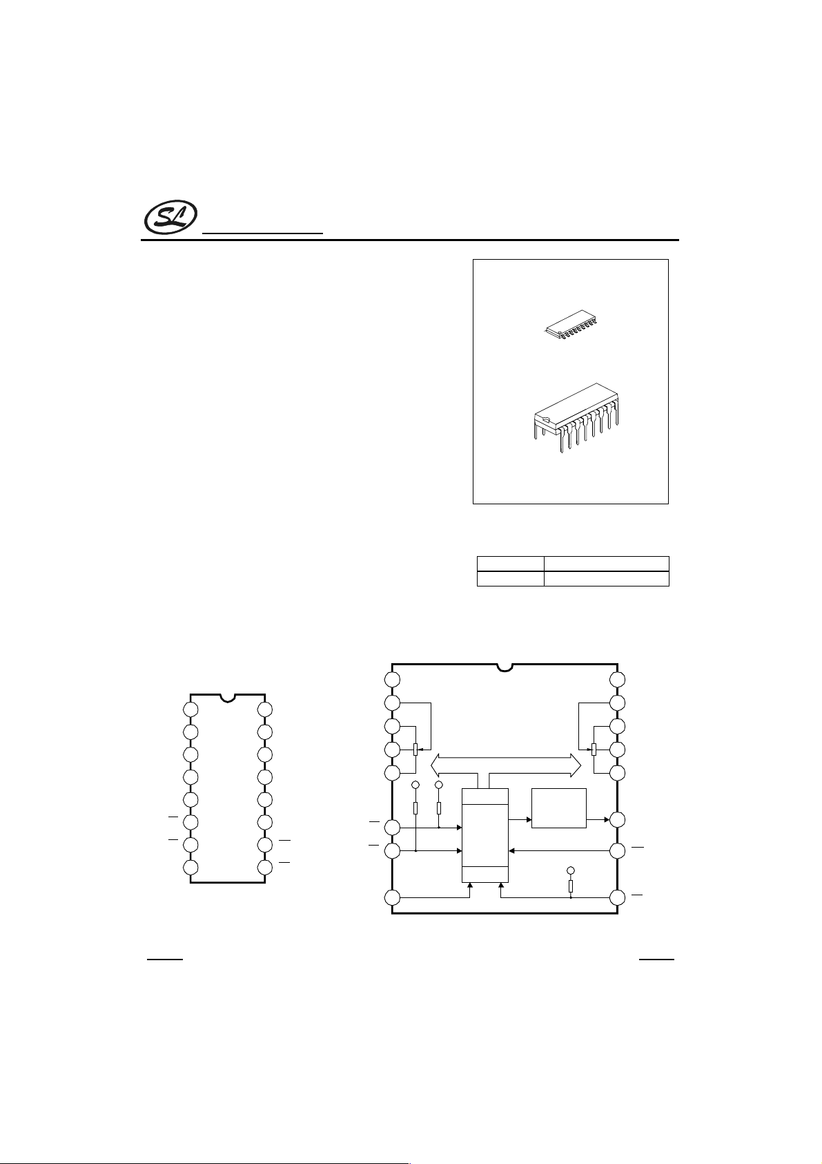
PIN CONFIGURATION BLOCK DIAGRAM
SC9235
SOP-16
DIP-16
ORDERING INFORMATION
SC9235 DIP-16 Package
SC9235S SOP-16 Package
V
16
15
14
13
12
11
10
9
DD
OUT-2
IN-2
TP-2
GND-2
DC-OUT
INH
INT
V
OUT-1
IN-1
TP-1
GND-1
OSC
V
SS
1
OUT-1
IN-1
TP-1
GND-1
OSC
UP
DN
2
3
4
5
DECODER
6
UP/DOWN
COUNTER
D-A
CONVERTER
7
CONTROL
8
SS
1
2
3
4
SC9235
5
UP
6
DN
7
8
16
15
14
13
12
11
10
9
DD
V
OUT-2
IN-2
TP-2
GND-2
DC-OUT
INH
INT
HANGZHOU SILAN MICROELECTRONICS JOINT-STOCK CO.,LTD
Rev: 1.0 2000.12.31
1
Page 2
Silan
Semiconductors
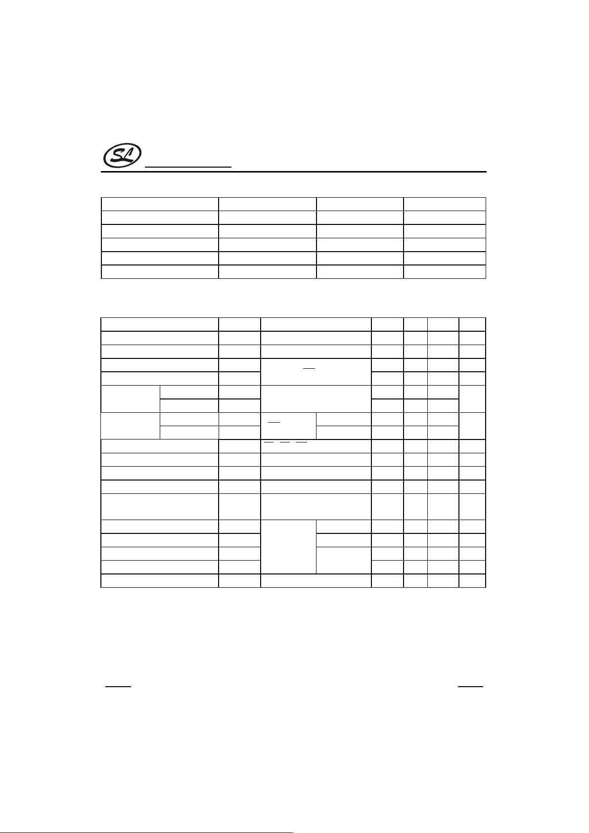
ABSOLUTE MAXIMUM RATINGS
Characteristic Symbol Value Unit
Supply Voltage V
Input Voltage V
PowerDissipation P
Operating Temperature Topr -40 ~ +85
Storage Temperature Tstg -55 ~ +150
ELECTRICAL CHARACTERISTICS
Parameter Symbol Test Conditions Min Typ Max Unit
Operating Supply Voltage V
Operating Supply Current I
Backup Voltage V
Backup Current I
Input Voltage
Input Current
Pull Up Resistor R
Volume Resistor R
Analog Switch ON Resistor R
Attenuation Error
Balance Between Left And Right
Total Harmonic Distortion THD 0dB -- 0.01 -- %
Maximum Attenuation ATT
Cross Talk
Output Noise Voltage V
OSC Frequency f
"H" Level V
"L" Level V
"H" Level I
"L" Level I
DD
DD
QD
QD
IH
IL
IH
IL
UP
VR
ON
∆ATT
∆R
VR
MAX
C.T
N
OSC
(Ta=25°C)
DD
IN
D
-0.3 ~15 V
-0.3V ~ VDD+0.3V V
300 mW
(Unless otherwise specified, Ta = 25k,V
Ta=-40 ~ 85°C
No load,fosc=20Hz -- 0.3 1.0
="L"
INH
All input pin
input pin
INH
UP,DN,INT
VIH=V
Input pin
V
=0V -1 -- 1
IL
0.7V
DD
BetweenINGND resistor 31 44 58
Analog switch ON resistor -- 500 800
-- -- 0
Volume resistor error between
left and right
F
1kHz
IN=
V
=1Vrms
IN
R
=100kΩ
L
Rg=600Ω
∞dB
0dB
Cx=2.2µF, Rx=33kΩ
HANGZHOU SILAN MICROELECTRONICS JOINT-STOCK CO.,LTD
2
SC9235
°C
°C
9V)
=
DD
4.5 9.0 12 V
2.0 -- 12 V
-- 0.01 1.0
-- V
DD
0--0.3V
-1 -- 1
23 47 71
-- 0
-- 100 -- dB
-- 100 -- dB
-- 2.0 --
-- 20 -- Hz
DD
DD
±2.0
±3.0
µVrms
Rev: 1.0 2000.12.31
µA
µA
µA
kΩ
kΩ
dB
V
Ω
%
Page 3
Silan
Semiconductors
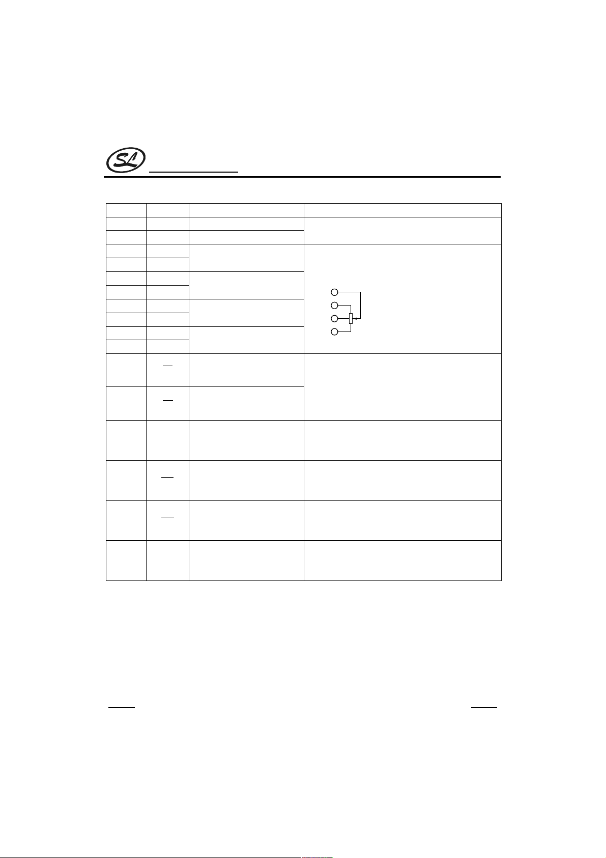
PIN DESCRIPTION
Pin No. Symbol Pin Name Description
1 Vss Negative power supply pin
16 V
2OUT-1
15 OUT-2
3IN-1
14 IN-2
4TP-1
13 TP-2
5 GND-1
12 GND-2
6
7
8 OSC Oscillation pin
9
10
11 DC-OUT DCoutput pin for level meter
UP
DN
INT
INH
Positive power supply pin
DD
Volume output pins
Volume input pins
Tap output pins for loudness
Analog ground pins
Volume up input pin
Volume down input pin
Initializing pin
Inhibit terminal
Power Supply terminal
Volume circuit
OUT
IN
TP
GND
Volume up, down control input pin.
The 1 step / 1 push volume is controlled by pushing
the Up or Down key . If the key has been pushed
continuously, the continuous volume control.
These two input pins have built-in pull-up resistor.
Oscillation pin.
Oscillator circuit consist of C.R connection.
Oscillation is executed while key is pushed.
Input pin for setting initial volume level volume level
set to 46dB by "L" input.
This input pin has built-in pull-up resistor.
Back up mode input pin.
Internal all operation is stopped by "L" input, and
volume level remains with low current consumption.
DC output pin for volume level meter.
DC voltage which is corresponded to volume step is
generated.
SC9235
HANGZHOU SILAN MICROELECTRONICS JOINT-STOCK CO.,LTD
Rev: 1.0 2000.12.31
3
Page 4

Silan
Semiconductors
FUNCTION DESCRIPTION
1. VOLUME CIRCUIT
Volume circuit consist of ladder resistor and analog switch.
Tap for loudness is connected to step 10 (20dB).
Attenuation is as follows when resistor (3.9kΩ) is connected between TP pin and pin.
SC9235
* Equivalence circuit
OUT
IN
28.5kΩ
TP
20.25kΩ
GND
* Volume step and attenuation
(Attenuation is as follows when resistor (3.9kΩ)is
connected between TP pin and GND pin.)
S
0
S
1
S
2
S
9
S
10
S
11
S
30
31
S
Step Attenuation Step Attenuation
0 0(dB) 16 32(dB)
1 2 17 34
2 4 18 36
3 6 19 38
4 8 20 40
5102142
6 12 *22 46
7142350
8162454
9182558
10 20 26 62
11 22 27 66
12 24 28 70
13 26 29 74
14 28 30 78
15 30 31
∞
* Step 22 (46dB) initial value.
HANGZHOU SILAN MICROELECTRONICS JOINT-STOCK CO.,LTD
Rev: 1.0 2000.12.31
4
Page 5

Silan
Semiconductors
2. VOLUME UP, DOWN CONTROL CIRCUIT
Volume up, down control is executed by UP , DN key input.
* The 1 step / 1 push volume is controlled by "L" level of
*If
UP , DN key is input "L" continuously, volume level is changed continuously.
* Timing of key input
UP / DN INPUT
VOLUME LEVEL
tT a
(f
OSC
=20Hz)
Note: t : Prevent time for chattering 2.21/fosc(110ms)
T: Switching time to automatic mode 101/fosc(500ms)
a : Up,Down speed 21/fosc(100ms)
foscCx•Rx(Hz) : Rx=12~220k
3. DC OUTPUT CIRCUIT FOR VOLUME LEVEL
DC output for volume level meter is internally connected to D−A converter (R/2R type).
8 stage output voltage which is corresponded to volume level is generated.
Because output impedance ≈ 22kΩ (typ.) is high, If input impedance of next setting level meter IC is low,
set to Buffer.
UP , DN key.
SC9235
Equivalence circuit
R≈22kΩ
HANGZHOU SILAN MICROELECTRONICS JOINT-STOCK CO.,LTD
2R
2R
2R
R
R
R
DC-OUT
* Volume step and Output voltage
Step Attenuation(dB) Output Voltage(V)
0~3 0~6 7/8VDD
4~7 8~14 6/8VDD
8 ~ 11 16 ~ 22 5/ 8 VDD
12 ~ 15 24 ~ 30 4/ 8 VDD
16 ~ 19 32 ~ 38 3/ 8 VDD
20 ~ 23 40 ~ 50 2/ 8 VDD
24 ~ 27 54 ~ 66 1/ 8 VDD
28 ~ 31
70 ~ ∞
Rev: 1.0 2000.12.31
5
0
Page 6

Silan
Semiconductors
4. INITIALIZATION AND BACKUP OPERATION
1) Initialization operation
When power on, volume level is set to initial value (46dB) by setting
DD
V
DD
V
SC9235
INT pin to "L" level for a while.
V
IL
0V
Adjust condenser value which is set INT pin to the period while INT pin is "L" level is longer than 1ms when
Power on.
2) Backup operation
Internal operation is all stopped when
Volume data is remains while Backup mode with low current consumption.
DD
V
0V
NORMAL MODE BACKUP MODE NORMAL MODE
tt≥1ms
INH pin is "L" level, and prohibit input and output.
V
DD
INH
INT
Back up
V
DD
2V
MIN≥2.0V
Minimum Voltagefor Back up is 2.0V.
Back up data is lost
HANGZHOU SILAN MICROELECTRONICS JOINT-STOCK CO.,LTD
Rev: 1.0 2000.12.31
6
Page 7

Silan
Semiconductors
TEST CIRCUITS
V
DD
AVIDD/I
QD
SC9235
V
V-M
L
R
1/2 VDD
THD —Vout
1
fin=1kHz,Rg=600Ω
RL=100kΩ,HPF=20Hz
LPF=80kHz
0.1
THD (%)
0.01
0.001
0.01 0.1 1 10
Vout (Vrms)
SG
R
X
VDD=6.0V
VDD=12.0V
600Ω
VDD=9.0V
SG
INH
47µF
V-M
R
L
1/2 VDD
V
DD
1
2
3
4
16
15
14
13
600Ω
SC9235
5
6
7
8
C
X
12
11
10
9
C
INT
LD CHARACTERISTIC
10
0
-10
-20
-30
-40
-50
-60
10 100 1000 10000 100000
fin (Hz)
HANGZHOU SILAN MICROELECTRONICS JOINT-STOCK CO.,LTD
Rev: 1.0 2000.12.31
7
Page 8

Silan
Semiconductors
TYPICAL APPLICATION CIRCUIT
SC9235
Condenser for Backup
V
SS
1
OUT
L-
ch
IN
1/2 V
DOWN Key
LEFT SIDE RIGHT SIDE
(Note) Loudness circuit is left side, only volume (without loudness) circuit is right side.
C1=1500pF C1=0.1µFR=8.2kΩ
DD
UP Key
C1
R
3.9kΩ
C2
2
3
4
5
6
UP
DN
7
Rx
Cx
OSC
8
LEVEL METER
V
DC-OUT
INH
INT
DRIVER IC
1/2 V
DD
DD
16
15
14
3.9kΩ
13
12
11
10
4.7kΩ
9
1/2 V
OUT
IN
+B
R-
ch
DD
HANGZHOU SILAN MICROELECTRONICS JOINT-STOCK CO.,LTD
Rev: 1.0 2000.12.31
8
Page 9

Silan
Semiconductors
PACKAGE OUTLINE
16-DIP-P-300 UNIT:mm
2.54
SC9235
0.25
6.40
3.51
19.4
1.50
0.46
7.62
15 degree
5.083.30
16-SOP-P-225 UNIT:mm
0.41
3.95
6.00
5.72
1.27
10.20
9.80
1.95
HANGZHOU SILAN MICROELECTRONICS JOINT-STOCK CO.,LTD
Rev: 1.0 2000.12.31
9
 Loading...