

Page 1
Silan
Semiconductors
TONE / PULSE SWITCHABLE DIALER
WITH HANDFREE FUNCTION
DESCRIPTION
The SC91710A/B are Tone/Pulse switchable dialer which are
fabricated in COMS technology with wide operating voltage for both
tone and pulse mode, and consumes very low memory retention
current in ON-HOOK state.
FEATURES
*Tone/Pulse switchable dialer
*One 32-digit last number redial memory
*Pulse-to-tone (P→T) is provided for PBX operation
*Flash key is available
*Minimum tone duration is 98ms or 83ms
*Minimum intertone pause is 98ms or 83ms
*Redial Pause time (0ms)
*Uses 3.579549MHz crystal or ceramic resonator
*Many options can be selected
Mode (10PPS; 20PPS; Tone)
M/B ratio (40:60;33:66)
Pause time (3.6s)
*Flash function (RESET)
(P→T) pause time (3.6s)
Flash time (600ms; 300ms; 100ms; or 80ms)
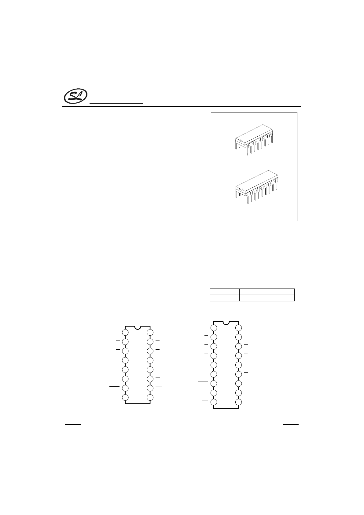
PIN CONFIGURATION
SC91710A/B
DIP-16
DIP-18
*Mixed dialing
*Power on reset circuit is provided
*Handfree function is provided for speaker
phone application
*Packaged in 16-DIP or 18-DIP
ORDERING INFORMATION
SC91710A
SC91710B
DIP-16 Packaged
DIP-18 Packaged
OSCI
OSCO
XMUTE
V
1
OSCI
OSCO
XMUTE
V
HFI
C2
2
C3
3
C4
4
C1
5
6
7
SS
8
9
1
C2
2
C3
3
C4
4
C1
5
6
7
8
SS
16
15
14
13
12
SC91710A
11
10
R3
R2
R1
R4
TONE
PO
HKS
9
V
DD
18
17
16
15
14
SC91710B
13
12
11
10
R3
R2
R1
R4
TONE
PO
HKS
V
DD
HFO
HANGZHOU SILAN MICROELECTRONICS JOINT-STOCK CO.,LTD
Rev: 2.0 2001-11-13
1
Page 2
Silan
Semiconductors
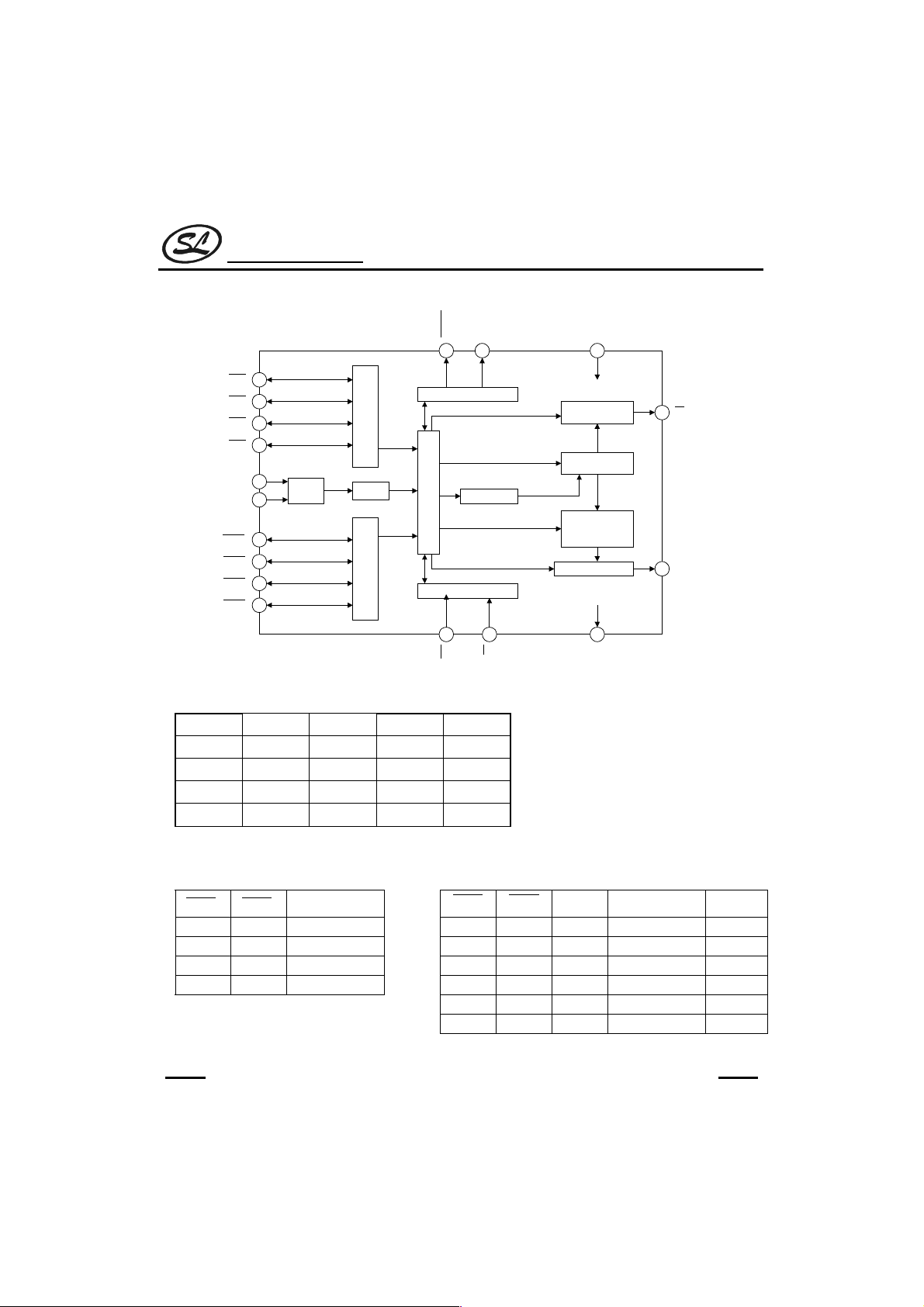
BLOCK DIAGRAM
XMUTE
HFO
SC91710A/B
VDD
COL1
COL2
COL3
COL4
OSCI
OSCO
ROW1
ROW2
ROW3
ROW4
OSC. DIVIDER
KEYBOARD ASSIGNMENT
C1 C2 C3 C4
R1
R2
R3
R4
123P→T
456F
789P
*or */T 0 # RD
COLUMN
ROW
INPUT INTERFACE CKT.
INTERFACECKT.
LNB MEMORY
KERNEL CONTROL CKT.
INTERFACECKT.
INPUT INTERFACE CKT.
HFI
HKS
PULSE
GENERATOR
DECODER &
DATA LATCH
ROW/COLUMN
PROGRAMMING
COUNTER
D/A CONVERTER
VSS
PO
TONE
1) P→T: In pulse mode, execute P→T function.
2) P: Pause key.
3) F: Flash key
4) RD: Redial key
5) In pulse mode, execute P→T function.
In tone mode, execte “
*
”key
DIALING SIGNAL OPTION
A: Flash time B:
Row3 Row4
Flash time(ms)
Row1 Row2
MODE PULSERATE M/B
NR NR 600 R NR TONE -- -NR R 300 R R TONE -- --
R NR 100 NR NR PULSE 20PPS 40:60
R R 80 NR R PULSE 20PPS 33:66
UR NR PULSE 10PPS 40:60
UR R PULSE 10PPS 33:66
HANGZHOU SILAN MICROELECTRONICS JOINT-STOCK CO.,LTD
Rev: 2.0 2001-11-13
2
Page 3
Silan
Semiconductors
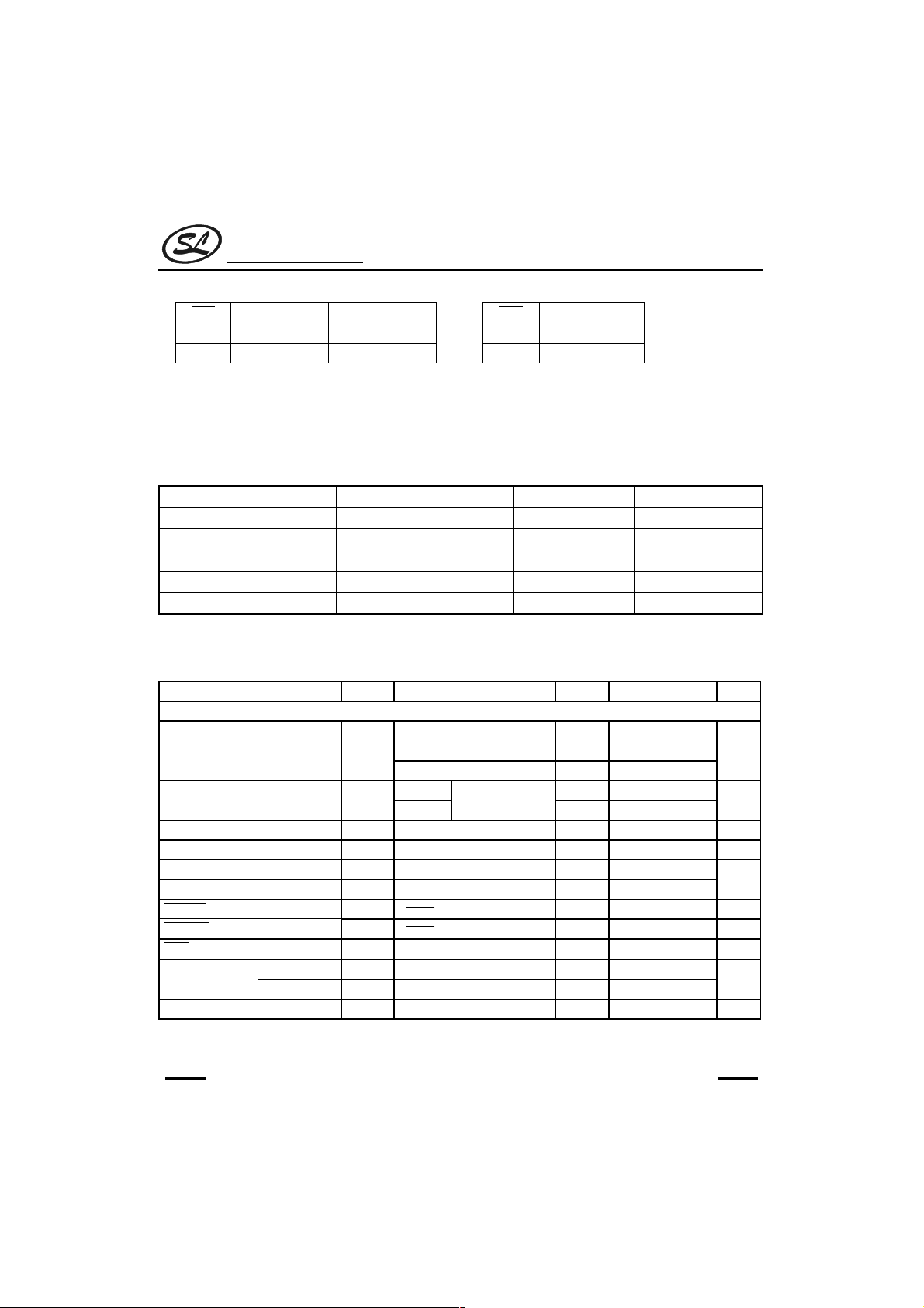
C: Tonefunction D: Key type select
Col1
NR 98ms 98ms NR *
Note: NR: no resistance
Tone Duration Inter-Tone Pause
R 83ms 83ms R */T
R: A resistance connect to V
UR: A resistance connect to V
(820kΩ typically)
SS
DD
Col2
ABSOLUTE MAXIMUM RATINGS
(Tamb=25°C, All voltage referenced to VSS, unless otherwise specified)
Characteristic Symbol Value Unit
Power Supply Voltage V
Input Voltage V
PowerDissipation P
Operating Temperature Topr -25~+70 °C
Storage Temperature Tstg -55~+150 °C
DD
IN
D
ELECTRICAL CHARACTERISTICS
(Tamb=25°C, VDD=2.5V,fosc=3.579545MHz, unless otherwise specified)
Parameter Symbol Conditions Min Typ Max Unit
DC Characteristics
Operating Voltage V
Operating Current I
Standby Current ISON-HOOKNo keypad entry -- 0.1 1 µA
Memory Retention Current Imr ON-HOOKVDD=1.0V -- 0.1 0.2 µA
Control Pin Input Low Voltage Vil -- V
Control Pin Input High Voltage Vih -- 0.7V
Pin Leakage Current
XMUTE
XMUTE
HKS
Scanning Pin
Key-in Debounce Time t
Pin Sink Current
Pin Input Current Ihks Vhks=2.5V -- -- 0.1 µA
Tone 2.5 -- 5.5
DD
Pulse 2.0 -- 5.5
Memory retention 1.0 5.5
Tone -- 0.6 2
OP
Pulse
V
Imth
V
Imtl
Drive Current Ikbd Vn=0Vnote1 41030Keyboard
Sink Current Ikbs Vn=2.5note1 200 400 800
-- -- 20 -- ms
DB
XMUTE
XMUTE
OFF-HOOK,
Keypad entry
=6.0V
=0.5V
SC91710A/B
*or */T select
6.0 V
-0.3~VDD+0.3 V
500 mW
-- 0.2 0.5
SS
DD
-- -- 1 µA
0.2 0.5 -- mA
0.3V
V
(to be continued)
mA
DD
DD
µA
V
V
HANGZHOU SILAN MICROELECTRONICS JOINT-STOCK CO.,LTD
Rev: 2.0 2001-11-13
3
Page 4
Silan
Semiconductors
(continued)
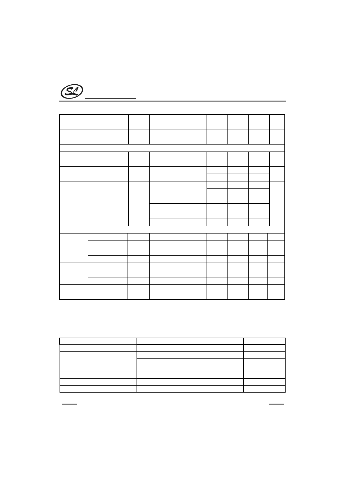
Parameter Symbol Conditions Min Typ Max Unit
HFI pin input resistor Rhfi VDD=2.5 -- 200 -- kΩ
HFO pin drive current Ihdoh Vhfo=2.0V 0.5 -- -- mA
HFO pin sink current Ihdol Vhfo=2.5V 0.5 -- -- mA
Pulse Mode
Pulse Output Pin Leakage Current Ipoh Vpo=2.5V 0.1 -- -- µA
Pulse Output Pin Sink Current Ipol Vpo=0.5V 0.5 -- -- mA
Pulse Rate fpr
Make/Break Ratio tMt
Pre-digit Pause t
Inter-digit Pause t
B
M/B ratio=40:60 -- 40 --
PDP
M/B ratio=33:66 -- 33 -Pulse rate=10pps -- 800 --
IDP
Pulse rate=20pps -- 500 --
Tone Mode
DC Level Vdc VDD=2.0V~5.5V 0.5V
Tone
Output Pin
Sink Current Itl Vdtmf=0.5V 0.2 -- -- mA
AC level Vdtmf RowgroupRL=10KΩ 130 155 170 mVrms
Load Resistor RI Dist.≤ -23dB 10 -- -- KΩ
=2.0~5.5 V,
V
DTMF Signal
Pre-emphasis twist
Distortion(note 2) Dist. R
Minimum tone duration Time t
Minimum Intertone Pause Time t
DD
Column-Row group
=10KΩ -- -30 -23 dB
L
Auto redial -- 98/83 -- ms
TD
Auto redial -- 98/83 -- ms
ITP
Note: 1. Vn: Input voltage of any keyboard scanning pin (Row group, Column group)
2
2
2Distortion (dB) = 20log{[V
: Row group and Column group signal , V1V2…Vn: Harmonic signal (BW = 300Hz~3500Hz
V
L,VH
1
+V
2
+V
+…Vn2)
2
3
2
1/2
]/[(V
2
1/2
+V
)
L
]}
H
SC91710A/B
-- 10 --
-- 20 --
-- 40:60 --
-- 33:66 --
DD
-- 0.7V
123dB
DD
pps
%
ms
ms
V
ACTUAL FREQUENCY OUTPUT
(fosc=3.579545MHz)
Keyboard Scanning Pin Standard(Hz) Output Deviation(%)
R1 f1 697 699 +0.28
R2 f2 770 766 -0.52
R3 f3 852 848 -0.47
R4 f4 941 948 +0.74
C1 f5 1209 1216 +0.57
C2 f6 1336 1332 -0.30
C3 f7 1477 1472 -0.34
HANGZHOU SILAN MICROELECTRONICS JOINT-STOCK CO.,LTD
Rev: 2.0 2001-11-13
4
Page 5
Silan
Semiconductors
PIN DESCRIPTION
Pin No.
SC91710A SC91710B
SC91710A/B
Pin Name Description
44
11
22
33
14 16
15 17
16 18
13 15
C1
C2
C3
C4
R1
R2
R3
R4
*Provides keyboard scanning.
*
pin is LOW, the column group stays in “HIGH” state and row group
HKS
stays in “LOW” state.
*The keypad is compatible with the standard dual contact matrix keyboard
(as figure1b), the inexpensive single contact keyboard (as figure 1a), and
electronic input (as figure 1c).
*When
Column connection or by electronic input (as shown in figure 1c).
*Activation of two or more keys will result in no response, except for single
key.
*To avoid keyboard-bouncing error, this chip provides built-in debounce
circuit. (The debounce time = 20ms)
Figure1a: Single contact form
is “LOW”, a valid key entry is defined by related Row &
HKS
Row
keyboard configuration
Row
Column
Figure1c: Electronic signal input keyboard configuration
Column
Figure1b: Dual contact form
Row
Column
keyboard configuration
V
DD
V
SS
V
DD
V
SS
*Oscillator input & output pins.
55OSCI
66OSCO
*The 3.579545MHz oscillator is formed by a built-in inverter inside of this
chip and by connecting a 3.579545MHz crystal or a ceramic resonator
across the OSCI and OSCO pins. (built-in feedback resistor and capacitor)
*When
generates a 3.579545 MHz clock.
is “LOW”, a valid key-in may turn on this oscillator and
HKS
(to be continued)
HANGZHOU SILAN MICROELECTRONICS JOINT-STOCK CO.,LTD
Rev: 2.0 2001-11-13
5
Page 6
Silan
Semiconductors
( continued )
Pin No.
SC91710
SC91710B
A
7
8 8 VSS *Negative power supply pin.
9 11 VDD *Positive power supply pin.
10 12
11 13
12 14 TONE
Pin Name Description
7
XMUTE
HKS
9
10 HFO
PO
HFI
*Mute output pins.
*NMOS open drain output structure.
*The output is in “LOW” state during dialing sequence (both Pulse and
Tone
mode) otherwise this pin is “high-impedance”.
*Long (continue) Mute.
*Hook switch input pin.
*When the handset is in ON-HOOK state, this pin must be pulled “high” in
order to disable the dialing operation and decrease the power
consumption.
*When in OFF-HOOK state, the
all function operation.
*Pulse output signal pin.
*NMOS open drain output structure.
*The output is “LOW” during pulse dialing and Flash operation, otherwise
this output is “floating”.
*Dual ToneMulti-frequency output pin.
*In TONE mode, when an entry of digit key (include *, # key), this pin will
send out a corresponding DTMF signal.
*The TONE pin provides minimum tone duration and minimum intertone
pause time to support rapid key-in. If key-in time is less than 100ms,
DTMF signal will last for 100ms; otherwise the tone duration will last as
long as the key is pressed.
* Handfree input control pin.
* Toggleinput structure, falling edge trigger.
* It is used to enable and disable Handfree function.
* With waveshaped by a built-in Schmit trigger, the bounce of input can be
eliminated by external R, C debounce circuit.
* A built-in pull down resistor is 200k typical.
* Handfree output control pin.
* Inverter output structure (normally ‘low’, active ‘high’).
* When a HFI pin is active, Handfree function will be enabled (HFO=1) or
disable (HFO=0).
* When the Handfree function is enable (HFO=1), after OFF-HOOK action,
it can reset Handfree function and HFO pin return to ‘low’ state.
SC91710A/B
pin must be pulled “low” state for
HKS
HANGZHOU SILAN MICROELECTRONICS JOINT-STOCK CO.,LTD
Rev: 2.0 2001-11-13
6
Page 7

Silan
Semiconductors
KEYBOARD OPERATION
Symbol definitions:
↑
a)
↓
b)
c)
d)
e) D1~Dn :
f) Dp1~Dpn :
g) Dt1~Dtn :
h) t
F
i) t
P
j) t
PT
k) t
FP
l) t
RP
m) LNB : Last number redial buffer.
ANormal Dialing
1. Digit Dialing
: OFF-HOOK or enable Hand Free function.
: ON-HOOK or disable Hand Free function.
:
Input level from low to high.
:
Input level from high to low.
Digit key1, 2, 3, 4, 5, 6, 7, 8, 9, 0, *, #, (C1~Cn is same as D1~Dn).
Pulse digit1, 2, 3, 4, 5, 6, 7, 8, 9, 0, (Cp1~Cpn is same as Dp1~Dpn).
Tone digit1, 2, 3, 4, 5, 6, 7, 8, 9, 0, *, #, (Ct1~Ctn is same as Dt1~Dtn).
:Flashtime.
: Pause time.
: Pulse to Tone wait time.
: Pause time for flash.
: Pause time for redial.
SC91710A/B
Procedure ↑ D1, D2…, Dn↓
Dial out Dt1, Dt2…, Dtn (in Tonemode)
Dial out Dp1, Dp2,…, Dpn (in Pulse mode)
LNB D1, D2…, Dn
2. Dialing with flash key
Procedure ↑ F,D1,D2…,Dn ↓
Dial out t
Dial out t
LNB D1,D2…,Dn
, Dt1, Dt2…, Dtn (in Tone mode)
F,tFP
, Dp1, Dp2, …, Dpn (in Pulse mode)
F,tFP
3. Dialing with P→Tkey
Procedure ↑ D1,D2…,P→T,…, Dn ↓
Dial out Dp1, Dp2, …, t
LNB D1,D2…,P→T,…, Dn
Note: If key in digit over maximum digit stored in LNB, then RD is inhibit even after on/off hook.
HANGZHOU SILAN MICROELECTRONICS JOINT-STOCK CO.,LTD
, …, Dpn (in Pulse mode)
PT
7
Rev: 2.0 2001-11-13
Page 8

Silan
Semiconductors
BMixed dialing
Procedure ↑D1, D2…, P→T , D9, D10 …, Dn↓
Dial out Dp1, Dp2, …, t
LNB D1, D2…, P→T , D9, D10 …, Dn
CRedial
LNB D1,D2…,Dn
Procedure ↑ RD ↓
Dial out t
Dial out t
Note: If key in digit over maximum digit stored in LNB, then RD is inhibit.
DPause Function
Procedure ↑ D1, D2…, Dn, P, C1 …, Cn ↓
Dial out Dt1, Dt2 ,…, Dtn, t
Dial out Dp1, Dp2, … Dpn , t
LNB D1,D2…,Dn,P,C1,C2…,Cn
,Dt9,Dt10…,Dtn
PT
, Dt1, Dt2…, Dtn (in Tone mode)
RP
, Dp1, Dp2,…, Dpn (in Pulse mode)
RP
, Ct1, Ctn (in Tone mode)
P
, Cp1 …, Cpn (in Pulse mode)
P
SC91710A/B
EFlash Function
1. Reset
Procedure ↑ D1, D2…, Dn, F, C1 …, Cn ↓
Dial out Dt1, Dt2,…, Dtn , t
Dial out Dp1, Dp2,…, Dpn , t
LNB C1,C2…,Cn
, Ct1 …, Ctn (in Tone mode)
F,tFP
, Cp1 …, Cpn (in Pulse mode)
F,tFP
Handfree Function operation:
A) To execute Handfree function: When HFO = ’low’, HFI pin is active, the Handfree function will be enabled (HFO
= ’high’)
B) Reset Handfree function:
a. OFF-HOOK action.
b. When HFO = ’high’, a HFI pin is active again, the Handfree function will be reset (HFO=’low’).
HANGZHOU SILAN MICROELECTRONICS JOINT-STOCK CO.,LTD
Rev: 2.0 2001-11-13
8
Page 9

Silan
Semiconductors
Operating flow chart of Handfree
HF
ON HKS
HF LINE
Note: ON: ON HKS; OFF: OFF HKS; HF: Pressed HF key
STATENO.
(0) INITIAL STATE F F 0
(1) ON HKS HF LINE F F 1
(2) OFF HKS LINE F F 0
(3) OFF HKS HF LINE F F 1
ON HKS
(0)
INITIAL
HF
(1)
OFF
ON
OFF HKS
HF LINE
PO XMUTE
OFF
HF
(3)
SC91710A/B
ON
OFF HKS
HF
LINE
HFO
(2)
* F: Floating
(Hi-impedance)
HANGZHOU SILAN MICROELECTRONICS JOINT-STOCK CO.,LTD
Rev: 2.0 2001-11-13
9
Page 10

Silan
Semiconductors
TEST CIRCUIT
Operation
1 2
current
V+
A
Standby
current
SC91710A/B
V+
A
DD
V
ROW
HKS V
V+
V
DD
SS
HKSV
HKS V
MODE
SS
TONE
HKSV
PO
V
V+
V
DD
SS
MODE
keyboard
3
Tone output voltage
keyboard
5 6
Pulse output sink current
(open drain structure)
V+
V
Flash
key
7
DD
SS
Keypad input current (row group)
A
A
VEXT
R*
C*
counter
and
AC meter
10KΩ
DP
DP
DT
HKSV
DD
V
SS
4
Tone distortion
keyboard
V+
HKSV
TONE
Spectrum
analyzer
V
V
DD
SS
Pulse output sink current
(inverter structure)
V+
V
DD
HKS
PO
MODE
A
V
VEXT
R*
C*
V
SS
8
keypad input current (column group)
A
COLUMN
HKS V
V+
V
DD
SS
10KΩ
2
2
2
2
2
Note: 1. Dist. (dB)=20log{[V
+V
+V
1
2
3
+…V
1/2
)
]/[(V
n
2
1/2
+V
)
L
]}
H
a. V1…Vn are extraneous frequencies (ie, inter modulation and harmonic), components in the 500Hz
to
3400Hz band.
b. V
are the individual frequency components of DTMF signal.
L,VH
c. Whether keyboard is pushed refer to the TONE mode time diagram.
2. Sink current Isink=I/(1-Duty Cycle), I is the net DC current measured from ampere meter.
3. R*, C* mean other column and row.
HANGZHOU SILAN MICROELECTRONICS JOINT-STOCK CO.,LTD
10
Rev: 2.0 2001-11-13
Page 11

Silan
Semiconductors
TIMING DIAGRAMS
HKS
SC91710A/B
KEY IN
XMUTE
PO
TONE
OSCO
HKS
KEY IN
XMUTE
PO
TONE
OSCO
3 2 3
t
DB
t
TDtITP
t
ITP
Normal dialing
Tone Mode Timming Diagram
3 2 3
t
DB
t
t
B
PDP
t
TDtIDP
t
M
t
IDP
Normal dialing
t
ITP
......High impedance
t
IDP
......High impedance
Pusle Mode Timming Diagram
HANGZHOU SILAN MICROELECTRONICS JOINT-STOCK CO.,LTD
Rev: 2.0 2001-11-13
11
Page 12

Silan
Semiconductors
TIMING DIAGRAMS
HKS
(continued)
SC91710A/B
KEY IN
XMUTE
PO
TONE
OSCO
KEY IN
XMUTE
TONE
HKS
PO
t
IDP
P→T
t
PT
3 2 3
t
DB
t
PDP
t
IDP
Timming Waveform for mixed dialing Operation
(by P→T key entry)
F
t
DB
t
F
t
ITP
......High impedance
OSCO
......High impedance
Flash key operating timming
HANGZHOU SILAN MICROELECTRONICS JOINT-STOCK CO.,LTD
Rev: 2.0 2001-11-13
12
Page 13

Silan
Semiconductors
TIMING DIAGRAMS
HKS
(continued)
SC91710A/B
KEY IN
XMUTE
PO
TONE
OSCO
HKS
KEY IN
XMUTE
PO
TONE
3
t
DB
t
ITP
Tone Mode Redial Timming Diagram
3
t
DB
t
IDP
2
t
ITP
2
t
IDP
RD
t
RP
RD
t
ITP
t
D
......High impedance
t
IDP
t
IDP
t
ITP
OSCO
......High impedance
Pulse Mode Redial Timming Diagram
HANGZHOU SILAN MICROELECTRONICS JOINT-STOCK CO.,LTD
Rev: 2.0 2001-11-13
13
Page 14

Silan
Semiconductors
TIMING DIAGRAMS
HKS
(continued)
SC91710A/B
KEY IN
*PULSE MODE
XMUTE
3 3
2
t
DB
t
PDP
t
IDP
P
t
t
IDP
t
P
IDP
PO
TONE
OSCO
*TONE MODE
t
DB
XMUTE
PO
t
t
ITP
ITP
t
P
t
ITP
TONE
OSCO
......High impendance
Pause key operating timming
HANGZHOU SILAN MICROELECTRONICS JOINT-STOCK CO.,LTD
Rev: 2.0 2001-11-13
14
Page 15

Silan
Semiconductors
TYPACAL APPLICATION CIRCUIT
820kΩx5
*
0
#
R/P
SC91710A/B
1
4
7
2
5
8
3
6
9
P
P→T
F
Ring
Tip
1N4004x4
TONE
20pps
10pps
120V
ZNR
MPSA42
14
15
16
13
R1
R2
R3
R4
C4 C3 C2 C1
3 2 1 4 8
VDD
PO
11 9 10
100kΩ
1µF
2.2kΩ
330kΩ
240kΩ
1N4148
HOOK
MPSA92
ON/OFF
100kΩ22MΩ
SC91710A
100µF
V
3.579545MHz
OSCI OSCO
5 6
DD
470kΩ
HKS
V
XMUTE
SS
TO HANDSET
TONE
12
7
Speech network
2wrieto4wire
16V
1N4148x2
5.1V
2kΩ
100µF
16V
C945
1µF
100kΩ
HANGZHOU SILAN MICROELECTRONICS JOINT-STOCK CO.,LTD
Rev: 2.0 2001-11-13
15
Page 16

Silan
Semiconductors
TYPACAL APPLICATION CIRCUIT
820kΩx6
SC91710A/B
1
4
7
*
2
5
8
0
3
6
9
#
R/P
P
P→T
F
120V
Ring
ZNR
Tip
1N4004x4
20pps
10pps
TONE
14
15
16
13
3 2 1 4 8
VDD
SC91710B
OSCI OSCO
3.579545MHz
5 6
KEY
V
SS
HFI
9
1µF
HF
TO HANDSET
XMUTE
7
PO
HKS
HFO
10
& Audio amplifier
Speech network
2wrieto4wire
R1
R2
R3
R4
C4 C3 C2 C1
47kΩ
13 12 11
47kΩ
100µF
16V
V
DD
TONE
14
0.2µF
100kΩ
1µF
200kΩ
1µF
5.1V
3.3kΩ
240kΩ
C954
330kΩ
200kΩ
C945
470kΩ
2.7kΩ
C954
HOOK ON/OFF
MPSA92
22MΩ
100kΩ
1N4148
HANGZHOU SILAN MICROELECTRONICS JOINT-STOCK CO.,LTD
Rev: 2.0 2001-11-13
16
Page 17

Silan
Semiconductors
CHIP TOPOGRAPHY
SC91710A/B
Size: 1.45 x 1.54 mm
2
PAD COORDINATES
No. Symbol X Y No. Symbol X Y
1
2
3
4
5
6
7
8
9
Note: The original point of the coordinate is the die center.
P1 -542.6 -238.0
P2 -542.6 -468.1
P3 -542.6 -602.5
P4 -315.0 -602.5
P5 -134.8 -602.5
P6 85.5 -602.5
P7 562.4 -439.1
P8 562.4 -277.6
P9 562.4 -93.6
(Unit: µm)
10
11
12
13 P13
14 P14 148.6
15 P15
16 P16
17 P17
18 P18
P10 562.4 88.5
P11 562.4 252.4
P12 562.4 445.8
562.4 603.8
-22.4
-251.0 603.8
-542.6 124.7
-542.6 -102.9
603.8
603.8
HANGZHOU SILAN MICROELECTRONICS JOINT-STOCK CO.,LTD
Rev: 2.0 2001-11-13
17
Page 18

Silan
Semiconductors
PACKAGE OUTLINE
DIP-16-300-2.54 UNIT: mm
2.54
SC91710A/B
0.25
6.40
19.4
3.51
0.46
1.50
7.62
15 degree
5.083.30
DIP-18-300-2.54 UNIT: mm
2.54
0.25
6.40
1.50
22.95
7.62
15 degree
3.51
0.46
5.083.30
HANGZHOU SILAN MICROELECTRONICS JOINT-STOCK CO.,LTD
Rev: 2.0 2001-11-13
18
 Loading...