

Page 1
Silan
Semiconductors
13 MEMORY TONE / PULSE DIALER
WITH REDIAL SAVE HANDFREE &
HOLD FUNCTION
DESCRIPTION
The SC91650A/B, SC91651A/B, SC91652A/B are 13-memory
Tone/Pulse switchable dialer with Last Number Redial(LNB) and
HOLD function, which are fabricated in COMS technology with wide
operating voltage for both tone and pulse mode, and consumes very
low memory retention current in ON-HOOK state.
FEATURES
*13-memory Tone/Pulse switchable dialer
*Three 16-digit one touch memory and ten 16-digit two touch
memory
One 32-digit last number redial memory
One 32-digit SAVE function for storing phone number in off hook
status
Note: only 15-digit/31-digit for Tone mode, 1-digit use to identify
tone mode
*Pulse-to-tone (P→T) is provided for PBX operation
*Flash key is available
*Minimum tone duration is 100ms for SC91650, SC91651 or 91ms
for SC91652
*Minimum intertone pause is 106ms for SC91650, SC91651 or
91ms for SC91652
*Uses 3.579545MHz crystal or ceramic resonator
*Many options can be selected
Mode (10PPS; 20PPS; Tone)
M/B ratio (40:60;33:66)
Pause time (3.6s;2.0s)
Pulse number (n;n+1;10-n)
Flash function (RESET;digit)
(P→T) pause time (3.6s;1.0s)
Flash time (80ms; 93ms; 100ms; 200ms; 300ms; 600ms)
Flash pause time (200ms; 1000ms)
* Redial pause time (1ms)
* Mixed dialing and cascade dialing is provided
* Handfree function is provided for speaker phone application
SC91650/1/2 A/B
DIP-18
DIP-22
*Power on reset circuit is provided
*Hold function is provided
* Keytone is provided
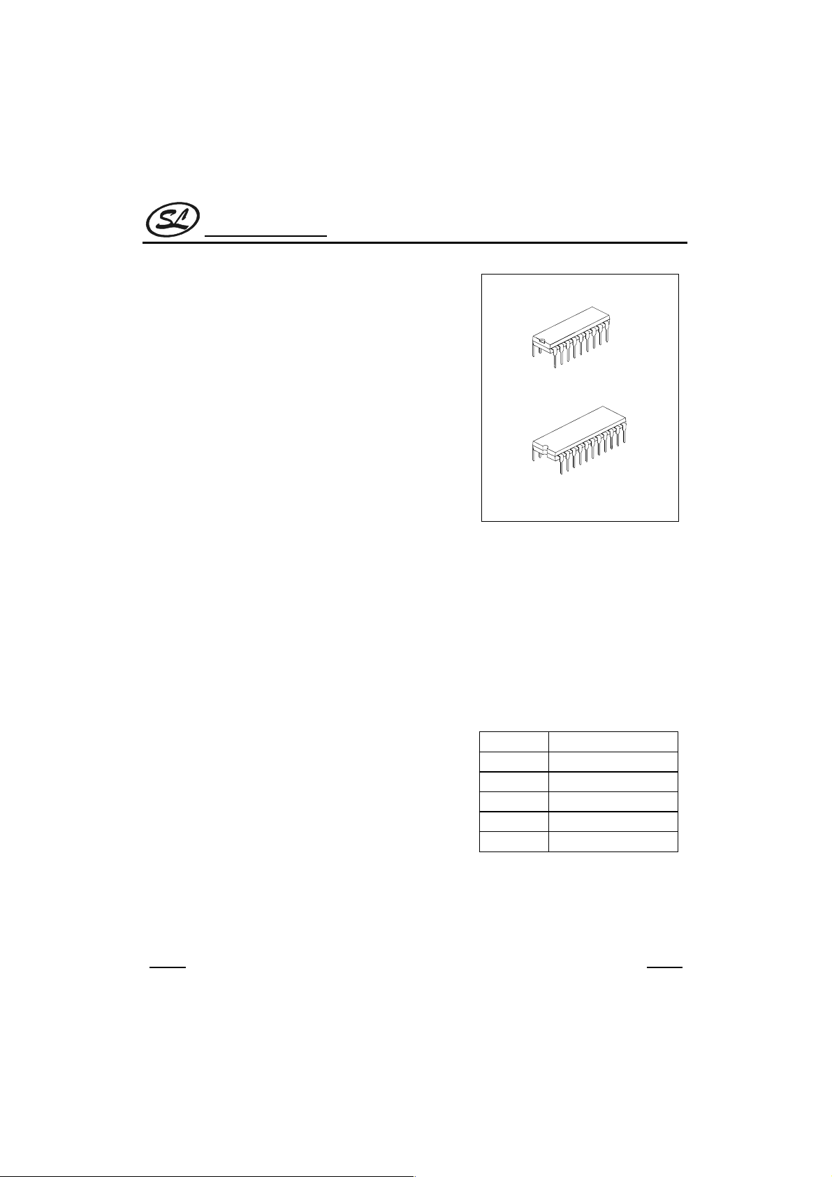
*Packaged in 18-DIP or 22-DIP
ORDERING INFORMATION
SC91650A DIP-18 Package
SC91650B
SC91651A
SC91651B
SC91652A
SC91652B
DIP-22 Package
DIP-18 Package
DIP-22 Package
DIP-18 Package
DIP-22 Package
HANGZHOU SILAN MICROELECTRONICS JOINT-STOCK CO.,LTD
REV: 1.0 2001.01.15
1
Page 2
Silan
Semiconductors
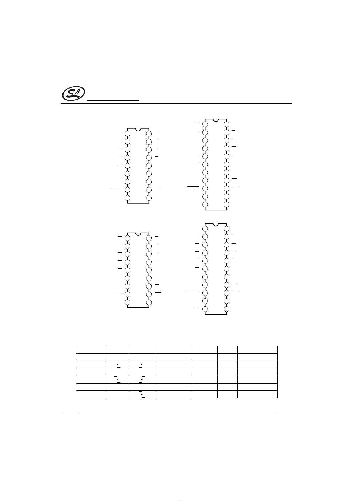
PIN CONFIGURATIONS
SC91650/1/2 A/B
OSCI
OSCO
XMUTE
V
1
HDI
2
1
C1
C2
2
3
C3
4
C4
5
C5
6
7
8
9
SS
18
17
16
15
14
SC91650/1A
13
12
11
10
R4
R3
R2
R1
MODE
TONE
PO
HKS
V
DD
C1
3
C2
4
C3
5
C4
6
C5
7
OSCI
OSCO
8
9
XMUTE HKS
V
10
SS
HFI
22
21
20
19
18
17
16
SC91650/1B
15
14
13
1211
HDO
R4
R3
R2
R1
MODE
TONE
PO
V
DD
HFO
OSCI
OSCO
XMUTE
V
1
PMUTE
2
1
C1
C2
2
3
C3
4
C4
5
C5
6
7
8
9
SS
18
17
16
15
14
SC91652A
13
12
11
10
R4
R3
R2
R1
MODE
TONE
PO
HKS
V
DD
C1
3
C2
4
C3
5
C4
6
C5
7
OSCI
OSCO
8
9
XMUTE HKS
V
10
SS
HFI
22
21
20
19
18
17
SC91652B
16
15
14
13
1211
KT
R4
R3
R2
R1
MODE
TONE
PO
V
DD
HFO
SELECTION GUIDE
HDI HFI PO PMUTE KT Tone Duration
SC91650A N N Inverter N N 100mS
SC91650B Inverter N N 100mS
SC91651A N N Open drain N N 100mS
SC91651B Open drain N N 100mS
SC91652A N N Open drain N N 91mS
SC91652B N Open drain Y Y 91mS
HANGZHOU SILAN MICROELECTRONICS JOINT-STOCK CO.,LTD
REV: 1.0 2001.01.15
2
Page 3
Silan
Semiconductors
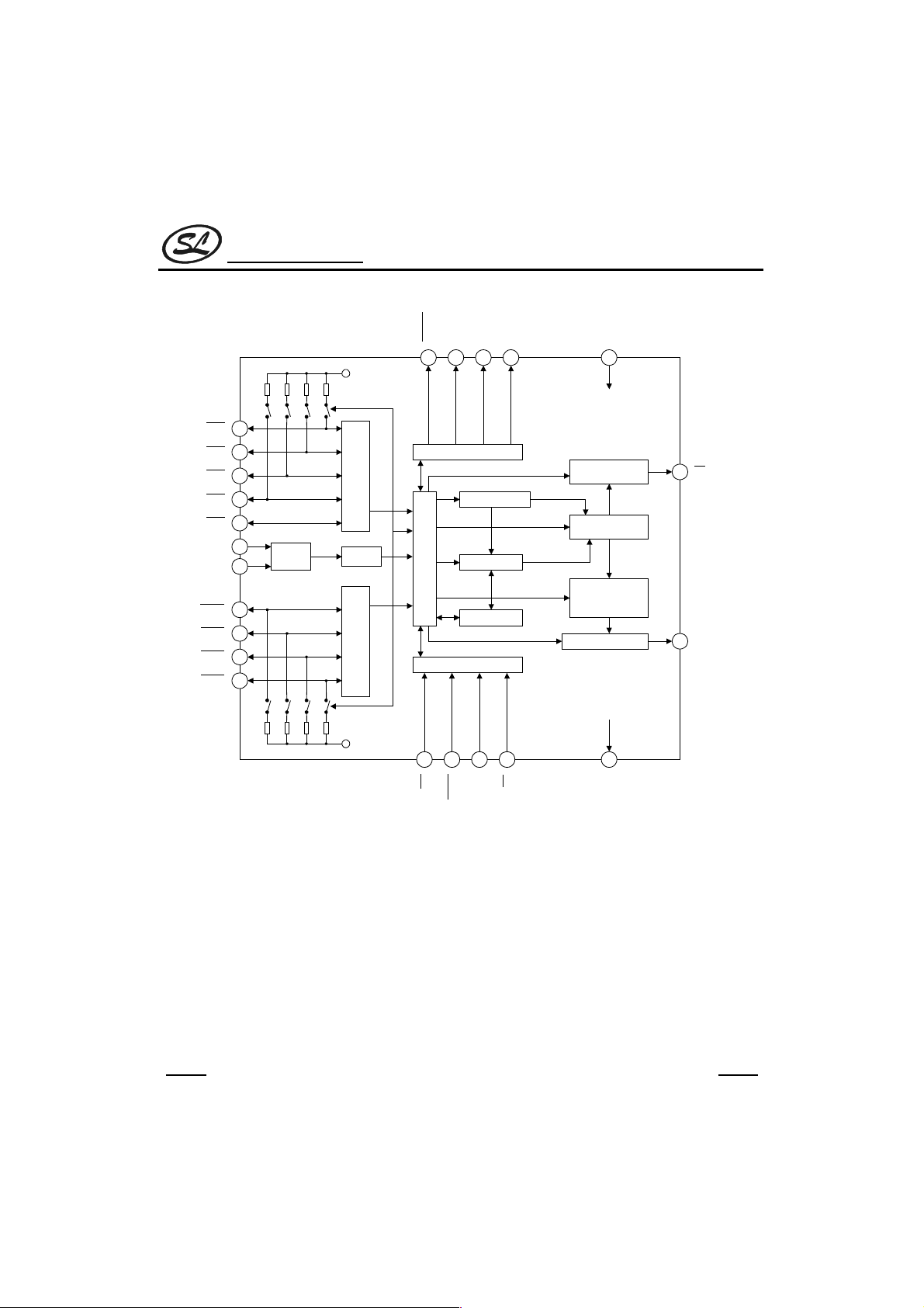
BLOCK DIAGRAM
COL1
COL2
COL3
COL4
COL5
OSCI
OSCO
ROW1
ROW2
ROW3
ROW4
OSC. DIVIDER
VDD
COLUMN
ROW
KT
XMUTE
INPUT INTERFACE CKT.
INTERFACE CKT.
INTERFACE CKT.
SAVE MEMORY
LNB MEMORY
KERNEL CONTROL CKT.
INPUT INTERFACE CKT.
SC91650/1/2 A/B
HFO
HDO
MEMORY
VDD
PULSE
GENERATOR
DECODER &
DATA LATCH
ROW/COLUMN
PROGRAMMING
COUNTER
D/A CONVERTER
PO
TONE
VDD
HFI
HKS
MODE
HDI
VSS
HANGZHOU SILAN MICROELECTRONICS JOINT-STOCK CO.,LTD
REV: 1.0 2001.01.15
3
Page 4
Silan
Semiconductors
KEYBOARD ASSIGNMENT
C1 C2 C3 C4 C5
R1
R2
R3
R4
1) */T: In pulse mode, execute P→T function; In TONE mode, execute * key
2) SAVE: SAVE key.
3) F: Flash key
4) RD/P: Redial key/Pause key
5) ST: Store key
6) EMn: One touch memory key
7) A: Auto key for two touch memory
123SAVEEM1
456FEM2
789AEM3
*/T 0 # RD/P ST
DIALING SIGNAL OPTION
The resistor connection between selected Row (or Column) and Vss may select most country telecom
specifications (refer to Row and Column pin description). Those options include M/B ratio, Flash time, pause time
…… , as follows.
a): Make/Break ratio: d): Flash time:
Row1
NR 40:60 NR NR 600
R 33:66 NR R 300
b): Pause time & P→T wait time: R R 200 *80
Row2
NR 3.6 3.6
R 2.0 1.0 e): Dialing out Pulse number:
c): Flash Key function: NR NR n
Column1
* for flash time = 80ms, 200ms only
tp(sec) tpT(sec) *for SC91652 only
NR Reset 0.2/0* R NR 10-n
R Digit 1.0 R R reserved
M/B ratio (%)
Flash key tFP(sec) NR R n+1
SC91650/1/2 A/B
Row3 Row4
R NR 93 *100
Column3 Column4
Flashtime(ms)
Pulse number
HANGZHOU SILAN MICROELECTRONICS JOINT-STOCK CO.,LTD
REV: 1.0 2001.01.15
4
Page 5
Silan
Semiconductors
Note: 1). NR = No resistor connection to Vss.
2). R = A resistor connection to Vss (820k typically).
3). N = Pressed digit key.
4). The following list is the corresponding pulse (break) numbers that are sent out by pressed the number
keys.
Digit key Normal (n) New Zealand (10-n) Sweden/Denmark (n+1)
11 9 2
22 8 3
33 7 4
44 6 5
55 5 6
66 4 7
77 3 8
88 2 9
99 1 10
010 10 1
*P→T KEY P→T KEY P→T KEY
# ignored ignored ignored
Dialing signal option
SC91650/1/2 A/B
ABSOLUTE MAXIMUM RATINGS
(Tamb=25°C, All voltage referenced to VSS, unless otherwise specified)
Characteristic Symbol Value Unit
Power Supply Voltage V
Input Voltage V
PowerDissipation P
Operating Temperature Topr -25~+70 °C
Storage Temperature Tstg -55~+150 °C
DD
IN
D
6.0 V
-0.3~VDD+0.3 V
500 mW
HANGZHOU SILAN MICROELECTRONICS JOINT-STOCK CO.,LTD
REV: 1.0 2001.01.15
5
Page 6
Silan
Semiconductors
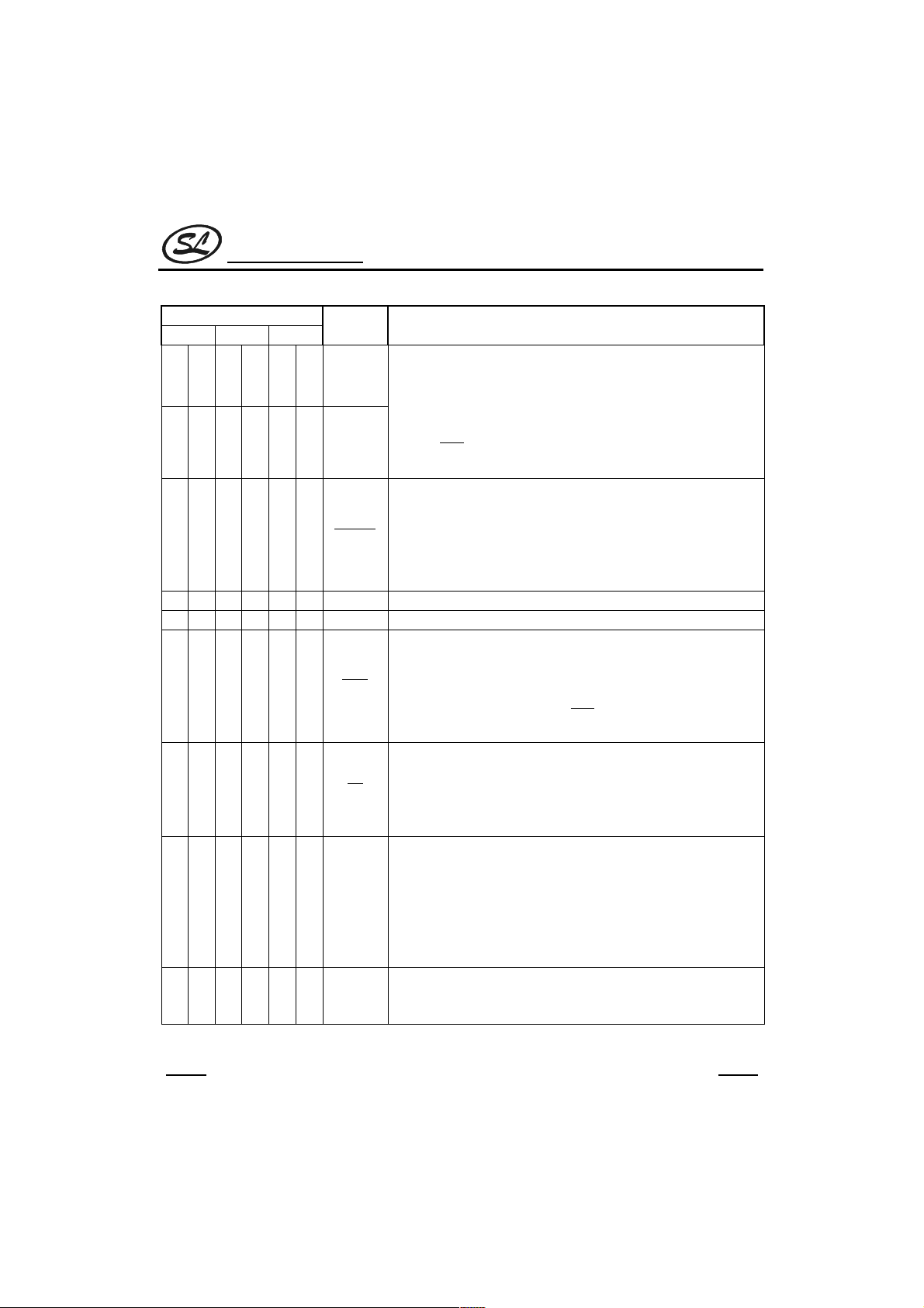
ELECTRICAL CHARACTERISTICS
(Tamb=25°C, VDD=2.5V,fosc=3.579545MHz, All voltage referenced to V
Parameter Symbol Conditions Min Typ Max Unit
DC Characteristics
Operating Voltage V
Operating Current I
Standby Current ISON-HOOKNo keypad entry -- 0.1 1.0 µA
Memory Retention Current Imr ON-HOOKVDD=1.0V -- 0.1 1.0 µA
Control Pin Input Low Voltage Vil -- V
Control Pin Input High Voltage Vih -- 0.7V
Pin Leakage Current
XMUTE
XMUTE
HKS Pin Input Current Ihks Vhks=2.5V -- -- 0.1 µA
Keyboard
Scanning Pin
Key-in Debounce Time t
HFI pin input resistor Rhfi VDD=2.5V -- 200 -- kΩ
HFO pin drive current Ihdoh Vhfo=2.0V 0.2 -- -- mA
HFO pin sink current Ihdol Vhfo=0.5V 0.2 -- -- mA
HDI
HDO pin drive current Ihdoh Vhdo=2.0V 0.2 -- -- mA
HDO pin sink current Ihdol Vhdo=0.5V 0.2 -- -- mA
Pulse Mode
Pulse Output Pin Leakage Current Ipoh Vpo=2.0V(SC91650 only) 0.2 -- -- mA
Pulse Output Pin Sink Current Ipol Vpo=0.5V 0.2 -- -- mA
Pulse Rate fpr
Make/Break Ratio tMt
Pin Sink Current
pin pull high resistor Rhdi VDD=2.5V -- 200 -- kΩ
DD
OP
Imth
Imtl
Drive Current Ikbd
Sink Current Ikbs
DB
Tone 2.0 -- 5.5
Pulse 2.0 -- 5.5
Memory retention 1.0 5.5
Tone -- 0.4 1
OFF-HOOK, Keypad
entry with pull down
resistance
Pulse
OFF-HOOK, No
Keypad entry
V
=6.0V
XMUTE
=0.5V
V
XMUTE
Vn=0Vnote1,
No resistors connected t o V
Vn=2.5note1
No resistors connected t o V
-- -- 20 -- ms
B
SC91650/1/2 A/B
unless otherwise specified)
SS,
V
DD
DD
mA
V
µA
pps
%
-- 0.2 0.5
20 80 µA
SS
DD
-- -- 1 µA
0.2 -- -- mA
21050
SS
200 400 800
SS
-- 10 --
-- 20 --
-- 40:60 --
-- 33:66 -(to be continued)
0.3V
V
HANGZHOU SILAN MICROELECTRONICS JOINT-STOCK CO.,LTD
REV: 1.0 2001.01.15
6
Page 7
Silan
Semiconductors
(continued)
Parameter Symbol Conditions Min Typ Max Unit
Pre-digit Pause t
Inter-digit Pause t
Tone Mode
DC Level Vdc VDD=2.0V~5.5V 0.5V
Tone
Output Pin
DTMF Signal
(note 3)
(note 3)
Note: 1. Vn: Input voltage of any keyboard scanning pin (Row group, Column group)
Sink Current Itl Vdtmf=0.5V 0.2 -- -- mA
AC level Vdtmf Row groupRL=5KΩ 130 155 180 mVrms
Load Resistor RI Dist.≤ -23dB 5 -- -- KΩ
Pre-emphasis twist
Distortion Dist. R
2Distortion (dB) = 20log{[V
V
: Row group and Column group signal , V1V2…Vn: Harmonic signal (BW = 300Hz ~ 3500Hz
L,VH
1
M/B ratio=40:60 -- 40 --
PDP
M/B ratio=33:66 -- 33 -Pulse rate=10pps -- 800 --
IDP
Pulse rate=20pps -- 500 --
=2.0~5.5 V,
V
DD
Column-Row group
=5KΩ -- -30 -23 dB
L
t
Auto redial
TD
t
Auto redial
ITP
2
+…Vn2)
1/2
]/[(V
2
2
+V
+V
2
3
SC91650/1/2 A/B
DD
123dB
-- 100 -- msMinimum tone duration Time
-- 91 -- ms
-- 106 -- msMinimum Intertone Pause Time
-- 91 -- ms
1/2
2
2
+V
)
L
]}
H
-- 0.7V
DD
ms
ms
V
ACTUAL FREQUENCY OUTPUT
(fosc=3.579545MHz)
Keyboard Scanning Pin Standard(Hz) Output Deviation(%)
R1 f1 697 699 +0.28
R2 f2 770 766 -0.52
R3 f3 852 848 -0.47
R4 f4 941 948 +0.74
C1 f5 1209 1216 +0.57
C2 f6 1336 1332 -0.30
C3 f7 1477 1472 -0.34
HANGZHOU SILAN MICROELECTRONICS JOINT-STOCK CO.,LTD
REV: 1.0 2001.01.15
7
Page 8
Silan
Semiconductors
PIN DESCRIPTION
Pin No.
650A/B 651A/B 652A/B
121212
232323
343434
SC91650/1/2 A/B
Pin Name Description
*Provides keyboard scanning.
C1
a. Dialling option:
*The resistor connection between selected Row (or Column) and Vss
may select most countries telecom specification.
C2
C3
R=820k
R1
R2
R3
R4
C4 C3 C2 C1
454545
565656
15 18 15 18 15 18
16 19 16 19 16 19
17 20 17 20 17 20
18 21 18 21 18 21
C4
C5
R1
R2
R3
R4
b. Keyboard scanning:
*While
state. While
pin is HIGH, Both column pin and row pin are in floating
HKS
pin is LOW, the c olumn group stays in “HIGH”
HKS
state and row group stays in “LOW” state.
*The keypad is compatible with the standard dual contact matrix
keyboard (as figure1b), the inexpensive single contact keyboard (as
figure 1a), and electronic input (as figur e 1c).
*When
is “LOW”, a valid key entry is defined by related Row &
HKS
Column connection or by electronic input (as shown in figur e 1c).
*Activation of two or more keys will result in no response, except for
single key.
*To avoid keyboard-bouncing error, this chip provides built-in
debounce circuit. (Th e debounce time = 20ms)
Row
Figure1a: Single contact form
keyboard configuration
Figure1c: Electronic signal input keyboard configuration
Column
Figure1b: Dual contact form
Row
Column
Row
Column
keyboard configuration
V
DD
V
SS
V
DD
V
SS
(to be continued)
HANGZHOU SILAN MICROELECTRONICS JOINT-STOCK CO.,LTD
REV: 1.0 2001.01.15
8
Page 9
Silan
Semiconductors
(continued)
Pin No.
650A/B 651A/B 652A/B
676767 OSCI
787878 OSCO
898989
9 10 9 10 9 10 VSS *Negative power supply pin.
10 13 10 13 10 13 VDD *Positive power supply pin.
11 14 11 14 11 14
12 15 12 15 12 15
13 16 13 16 13 16 TONE
14 17 14 17 14 17 MODE
Pin Name Description
*Oscillator input & output pins.
*The 3.579545MHz oscillator is formed by a built-in inverter inside of
this chip and by connecting a 3.579545MHz crystal or a ceramic
resonator across the OSCI and OSCO pins. (built-in feedback resistor
and capacitor)
*When
HKS
generates a 3.579545 MHz clock.
*Mute output pins.
*NMOS open drain output structure.
XMUTE
HKS
PO
*The output is in “LOW” state during dialing sequence (both Pulse
and Tone mode) and in Hold status otherwise this pin is
“high-impedance”.
*Long (continue) Mute.
*Hook switch input pin.
*When the handset is in ON-HOOK state, this pin must be pulled
“high” in order to disable the dialing operation and decrease the
power consumption.
*When in OFF-HOOK state, th e
for all function operation.
*Pulse output signal pin.
*Inverter output structure (SC91650).
*The output is “LOW” during pulse dialing and Flash operation,
otherwise this output is “high”.
*NMOS open drain output structure.
*Dual ToneMulti-frequency output pin.
*In TONE mode, when an entry of digit key (include *, # key), this pin
will send out a corresponding DTMF signal.
*The TONE pin provides minimum tone duration (tTD) and minimum
intertone pause time to support rapid key-in. If key-in time is less than
t
100ms), DTMF signal will last for t
TD (
duration will last as long as the key is pressed.
*Mode select pin.
*Tri-state input structure.
*This pin can select following three modes.
SC91650/1/2 A/B
is “LOW”, a valid key-in may turn on this oscillator and
pin must be pulled “low” state
HKS
100ms); otherwise the tone
TD (
(to be continued)
HANGZHOU SILAN MICROELECTRONICS JOINT-STOCK CO.,LTD
REV: 1.0 2001.01.15
9
Page 10

Silan
Semiconductors
(continued)
Pin No.
650A/B 651A/B 652A/B
11 11 HFI
12 12 12 HFO
11
22 22 HDO
SC91650/1/2 A/B
Pin Name Description
*Handfree input control pin. (SC91650, SC91651)
*Toggle input structure, rising edge trigger.
*It is used to enable and disable Handfree funtion.
*With waveshaped by a built-in Schmit trigger, the bounce of input
can be eliminated by external R
* A built-in pull down resistor is 200kΩ typical.
HFI
11
HDI
22 KT
1PMUTE
* Toggle input structure with pull up resistance 200kΩ, falling edge
trigger. (SC91652)
* Handfree output pin.
* Inverter output structure (normally ‘low’, active ‘high’).
* When a HFI pin is active, Handfree function will be enabled
(HFO=1) or disable (HFO=0).
* When the Handfree function is enable (HFO=1), after OFF-HOOK
action, it can reset Handfree function and HFO pin return to ‘low’
state.
*Hold line input control pin.
*Toggle input structure, falling edge trigger.
*It is used to enable and disable Hold line function.
*With waveshaped by a built-in Schmit trigger, the bounce of input
can be eliminated by extenal R.C debounce circuit.
*A built-in pull up resistor is 200kΩ typically.
*Hold line output pin.
*Inverter output structure, falling edge trigger.
*When a falling edge signal triggered
be enable (HDO=1) or disabled(HDO=0).
*When the Hold line function is enable (HDO=1), after OFF-HOOK
action or HFO pin is from “low” to “high”, it can reset Hold line
function and HDO pin return to “low” state.
*Keytone output pin for ralid key pad input and memory stored
(SC91652 only).
*CMOS invertor output structure.
*It will issue a 1.2kHz, duty cycle 50% signal with duration 30ms.
*To prevent signal interference, while DTMF issue, it will disable
Keytone output except function key.
*Pulse mode mute.
*CMOS inverter output structure.
*The output is high state during dialing sequence (pulse mode only),
otherwise this pin is low.
C debounce circuit.
•
pin, Hold line function will
HDI
HANGZHOU SILAN MICROELECTRONICS JOINT-STOCK CO.,LTD
REV: 1.0 2001.01.15
10
Page 11

Silan
Semiconductors
KEYBOARD OPERATION
Symbol definitions:
↑
a)
↓
b)
c)
d)
e) D1~Dn :
f) Dp1~Dpn :
g) Dt1~Dtn :
h) t
F
i) t
P
j) t
PT
k) t
FP
l) t
RP
m) LNB : Last number redial buffer.
M
n)
1 … Mm
ANormal Dialing
1. Digit Dialing
: OFF-HOOK or enable Hand Free function.
: ON-HOOK or disable Hand Free function.
:
Input level from low to high.
:
Input level from high to low.
Digit key1, 2, 3, 4, 5, 6, 7, 8, 9, 0, *, #, (C1~Cn is same as D1~Dn).
Pulse digit1, 2, 3, 4, 5, 6, 7, 8, 9, 0, (Cp1~Cpn is same as Dp1~Dpn).
Tone digit1, 2, 3, 4, 5, 6, 7, 8, 9, 0, *, #, (Ct1~Ctn is same as Dt1~Dtn).
:Flashtime.
: Pause time.
: Pulse to Tone wait time.
: Pause time for flash.
: Pause time for redial.
: Memory location; 1, 2, 3, 4, 5, 6, 7, 8, 9, 0.
SC91650/1/2 A/B
Procedure ↑ D1, D2…, Dn↓
Dial out Dt1, Dt2…, Dtn (in Tone mode)
Dial out Dp1, Dp2,…, Dpn (in Pulse mode)
LNB D1, D2…, Dn
2. Dialing with flash key
Procedure ↑ F,D1,D2…,Dn ↓
Dial out t
Dial out t
LNB D1, D2…, Dn (reset function only)
LNB : Un change (Digit Function only)
, Dt1, Dt2…, Dtn (in Tone mode)
F,tFP
, Dp1, Dp2, …, Dpn (in Pulse mode)
F,tFP
3. Dialing with P→Tkey
Procedure ↑ D1,D2…,P→T,…, Dn ↓
Dial out Dp1, Dp2, …, t
LNB D1,D2…,P→T,…, Dn
Note: If key in digit over maximum digit stored in LNB, then RD is inhibit even after on/off hook.
, …, Dpn (in Pulse mode)
PT
HANGZHOU SILAN MICROELECTRONICS JOINT-STOCK CO.,LTD
11
REV: 1.0 2001.01.15
Page 12

Silan
Semiconductors
BMixed dialing
SC91650/1/2 A/B
Procedure
Dial out Dp1, Dp2, …, t
LNB D1, D2…, P→T , D9, D10 …, Dn
↑D1, D2…, MODE=
↑D1, D2…, P→T , D9, D10 …, Dn↓
,Dt9,Dt10…,Dtn
PT
CRedial
LNB D1,D2…,Dn
Procedure ↑ RD ↓
Dial out t
Dial out t
Note: If key in digit over maximum digit stored in LNB, then RD is inhibit.
, Dt1, Dt2…, Dtn (InTone mode)
RP
, Dp1, Dp2,…, Dpn (in Pulse mode)
RP
DPause Function
Procedure ↑ D1, D2…, Dn, P, C1 …, Cn ↓
Dial out Dt1, Dt2 ,…, Dtn, t
Dial out Dp1, Dp2, … Dpn , t
LNB D1,D2…,Dn,P,C1,C2…,Cn
, Ct1, Ctn (in Tone mode)
P
, Cp1 …, Cpn (in Pulse mode)
P
EFlash Function
1. Reset
Procedure ↑ D1, D2…, Dn, F , C1 …, Cn ↓
Dial out Dt1, Dt2,…, Dtn , t
Dial out Dp1, Dp2,…, Dpn , t
LNB C1,C2…,Cn
, Ct1 …, Ctn (in Tone mode)
F,tFP
F,tFP
,D9,D10…, Dn↓;or
, Cp1 …, Cpn (in Pulse mode)
2 Digit
Procedure ↑ D1, D2…, Dn, F , C1 …, Cn ↓
Dial out Dt1, Dt2,…, Dtn , t
Dial out Dp1, Dp2,…, Dpn , t
LNB D1,D2…,Dn
, Ct1 …, Ctn (in Tone mode)
F,tFP
, Cp1 …, Cpn (in Pulse mode)
F,tFP
HANGZHOU SILAN MICROELECTRONICS JOINT-STOCK CO.,LTD
REV: 1.0 2001.01.15
12
Page 13

Silan
Semiconductors
FOne Touch Memory Function
1. Store Memory
Procedure ↑ ST, D1, D2…, Dn, ST, EMn ↓
Dial out Nothing
EMn = D1, D2,…… Dn
Procedure ↑ ST, D1, D2……,F,…… Dn, ST, EMn ↓
Dial out Nothing
EMn = D1, D2,……,F, ……Dn
Procedure ↑ ST, D1, D2……,P, …… Dn, ST, EMn ↓
Dial out Nothing
EMn = D1, D2,……,P, ……Dn
Procedure ↑ ST, D1, D2……,P→T, …… Dn, ST, EMn ↓
Dial out Nothing
EMn = D1, D2,……, P→T, ……Dn
2 Quickly Store
Procedure ↑ ST, D1, D2, ST, EM1, ST, D3, D4, D5, St, EM2, ST, EMn ↓
Dial out Nothing
EM1 = D1, D2; EM2 = D3, D4, D5, EMn = D3, D4, D5
LNB D1,D2…,Dn
SC91650/1/2 A/B
3 Redial
EMn = D1 , D2, ……Dn
Procedure ↑ EMn ↓
Dial out Dt1, Dt2, …… Dtn (in tone mode)
Dial out Dp1, Dp2, …… Dpn (in pulse mode)
LNB D1, D2,……Dn
GTwo Touch Memory Function
1. Store Memory
Procedure ↑ ST, D1, D2…, Dn, ST, EMn ↓
Dial out Nothing
EMn = D1, D2,…… Dn
Procedure ↑ ST, D1, D2……,F,…… Dn, ST, EMn ↓
Dial out Nothing
EMn = D1, D2,……,F, ……Dn
Procedure ↑ ST, D1, D2……,P, …… Dn, ST, EMn ↓
Dial out Nothing
EMn = D1, D2,……,P, ……Dn
HANGZHOU SILAN MICROELECTRONICS JOINT-STOCK CO.,LTD
13
REV: 1.0 2001.01.15
Page 14

Silan
Semiconductors
Procedure ↑ ST, D1, D2……,P→T, …… Dn, ST, EMn ↓
Dial out Nothing
EMn = D1, D2,……, P→T, ……Dn
2 Quickly Store
Procedure ↑ ST, D1, D2, ST, EM1, ST, D3, D4, D5, St, EM2, ST, EMn ↓
Dial out Nothing
EM1 = D1, D2; EM2 = D3, D4, D5, EMn = D3, D4, D5
LNB D1,D2…,Dn
3 Redial
EMn = D1 , D2, ……Dn
Procedure ↑ EMn ↓
Dial out Dt1, Dt2, …… Dtn (in tone mode )
Dial out Dp1, Dp2, …… Dpn (in pulse mode)
LNB D1, D2,……Dn
HSave Function
1. The Second Redial Memory
Procedure ↑ D1, D2 , …… Dn, dialing end, SAVE ↓
Dial out Dt1, Dt2 , …… Dtn (in tone mode)
Dial out : Dp1, Dp2, …… Dpn (in pulse mode)
LNB D1, D2, …… Dn
SC91650/1/2 A/B
2 Store Phone Number In Conversation
Procedure ↑ ST, D1, D2, …… Dn, conversation, ST, C1, C2, …… Cn, ST, SAVE ↓
Dial out Dt1, Dt2 , …… Dtn (in tone mode)
Dial out : Dp1, Dp2, …… Dpn (in pulse mode)
SAVE : C1, C2, …… Cn
LNB : C1, C2, …… Cn
Note: If key in digit over maximum digit stored in SAVE, then SAVE is ignore.
The data in SAVE is no change, and can dial out after on/off hook.
3 Redial
SAVE : D1, D2, …… Dn
Procedure ↑ SAVE ↓
Dial out Dt1, Dt2, …… Dtn (in tone mode )
Dial out Dp1, Dp2, …… Dpn (in pulse mode)
LNB D1, D2,……Dn(SC91652 only)
LNB : Un change (SC91650, SC91651)
HANGZHOU SILAN MICROELECTRONICS JOINT-STOCK CO.,LTD
REV: 1.0 2001.01.15
14
Page 15

Silan
Semiconductors
ICascade Dialing
1. Normal Dialing and Memory
Procedure ↑ D1,D2,……Dn,EM1,EMm…EMn,A,Mn↓
2. One Touch Memory and Memory
Procedure ↑ EMm……Emn,A,Mn↓
3. LNB and Memory
Procedure ↑ RD, EM1, EMm …… EMn, A, Mn ↓
4. SAVEand Memory for SC91652 only
Procedure ↑ SAVE, EM1, EMm …… EMn, A, Mn ↓
Handfree Function operation:
A) To execute Handfree function: When HFO = ’low’, HFI pin is active, the Handfree function will be enabled (HFO
= ’high’)
B) Reset Handfree function:
a. OFF-HOOK action.
b. When HFO = ’high’, a HFI pin is active again, the Handfree function will be reset (HFO=’low’).
c. When HDO pin is from “low” to “high”, the Handfree function will be reset (HFO=”low”).
SC91650/1/2 A/B
Hold Line Function Operation:
A) To execute Hold Line function: When HFO = ’high’ state or HKS is low, HDI pin is active, the Hold line function
will be enable ( HDO = ”high” ). The
pin keep to “low”, when HDO stays in “high” state.
XMUTE
B) Reset Hold Line function:
a. OFF-HOOK action.
b. HFO pin from “low” to: “HIGH level.
c. When HDO = ”high”, HDI pin is active, the Hold line function will be disabled (HDO=”low”).
Operating flow
chart of Handfree
HD
ON HKS
(0)
INITIAL
HD
HF
ON HKS
HF LINE
HF
ON HKS
HF LINE
HF
OFF
(1)
HD
(5)
OFF
ON
OFF HKS
HF LINE
OFF
HF
(3)
HD
ON
OFF HKS
(2)
LINE
HD
OFF HKS
LINE
HD
(4)
HF
HF
ONON
HANGZHOU SILAN MICROELECTRONICS JOINT-STOCK CO.,LTD
REV: 1.0 2001.01.15
15
Page 16

Silan
Semiconductors
(0) INITIAL STATE 0/F F 0 0
(1) ON HKS HF LINE 1/F F 1 0
(2) OFF HKS LINE 1/F F 0 0
(3) OFF HKS HF LINE 1/F F 1 0
(3) OFF HKS HD LINE 1/F 0 0 1
(3) ON HKS HD LINE 1/F 0 0 1
TEST CIRCUIT
STATE NO.
Operation
1 2
current
keyboard
PO XMUTE
V+
A
V
DD
MODE
HKS V
SS
DP
DP
DT
SC91650/1/2 A/B
HFO
Standby
current
HDO
ON/OFF: ON/OFF HKS
HF: Depress HF key
HD: Depress HF key
F: Floating (Hi-impedance)
is floating for SC91651/
PO
SC91652 open drain
struc-ture.
V+
A
HKSV
DD
V
SS
3
Tone output voltage
keyboard
5 6
Pulse output sink current
(open drain structure)
Flash
key
7
Keypad input current (row group)
V+
DD
V
SS
V+
V
DD
PO
HKSV
SS
A
V
ROW
HKS V
V+
SS
HKSV
DD
TONE
V
MODE
A
VEXT
R*
C*
counter
and
AC meter
10KΩ
4
Tone distortion
keyboard
V+
HKSV
TONE
Spectrum
analyzer
V
DD
V
SS
Pulse output sink current
(inverter structure)
V+
V
DD
HKS
PO
MODE
A
V
VEXT
R*
C*
V
SS
8
keypad input current (column group)
A
COLUMN
HKS V
V+
DD
V
SS
10KΩ
HANGZHOU SILAN MICROELECTRONICS JOINT-STOCK CO.,LTD
REV: 1.0 2001.01.15
16
Page 17

Silan
Semiconductors
Note: 1. Dist. (dB)=20log{[V
2
+V
1
2
2
2
2
+…V
1/2
)
]/[(V
n
+V
L
H
+V
2
3
a. V1…Vn are extraneous frequencies (ie, inter modulation and harmonic), components in the 500Hz
to 3400Hz band.
b. V
are the individual frequency components of DTMF signal.
L,VH
c. Whether keyboard is pushed refer to the TONE mode time diagram.
2. Sink current Isink=I/(1-Duty Cycle), I is the net DC current measured from ampere meter.
3. R*, C* mean other column and row.
TIMING DIAGRAMS
HKS
SC91650/1/2 A/B
2
1/2
)
]}
KEY IN
XMUTE
**PO
TONE
OSCO
HKS
KEY IN
PMUTE
XMUTE
**PO
TONE
OSCO
3 2 3
t
DB
tTDt
ITP
t
ITP
Normal dialing
Tone Mode Ti mming Diagram
3 2 3
t
DB
t
PDP
t
B
tTDt
IDP
t
M
t
IDP
Normal dialing
Pusle Mode Timming Diagram
t
ITP
......High impedance
t
IDP
......High impedance
HANGZHOU SILAN MICROELECTRONICS JOINT-STOCK CO.,LTD
REV: 1.0 2001.01.15
17
Page 18

Silan
Semiconductors
TIMING DIAGRAMS
HKS
(continued)
SC91650/1/2 A/B
KEY IN
XMUTE
**PO
TONE
OSCO
HKS
KEY IN
MODE
XMUTE
**PO
TONE
OSCO
t
IDP
P→T
t
PT
t
ITP
3 2 3
t
DB
t
PDP
t
IDP
......High impedance
Timming Waveform for mixed dialing Operation (by */T key entry)
for SC91650, SC91651
3 2 3
t
DB
t
PDP
t
t
IDP
t
IDP
PT
t
ITP
......High impedance
Timming Waveform for mixed dialing Operation (by mode selection pin switches)
for SC91650, SC91651
HANGZHOU SILAN MICROELECTRONICS JOINT-STOCK CO.,LTD
REV: 1.0 2001.01.15
18
Page 19

Silan
Semiconductors
TIMING DIAGRAMS (continued)
HKS
SC91650/1/2 A/B
KEY IN
XMUTE
PO
DTMF
OSCO
KEY IN
XMUTE
TONE
3 2 3
t
DB
t
PDP
t
IDP
*/T
t
t
IDP
PT
t
ITP
......High impedance
Timming Waveform for mixed dialing Operation (by */T key entry)
for SC91652 only
HKS
F
t
DB
PO
t
F
OSCO
......High impedance
Flash key operating timming
HANGZHOU SILAN MICROELECTRONICS JOINT-STOCK CO.,LTD
REV: 1.0 2001.01.15
19
Page 20

Silan
Semiconductors
TIMING DIAGRAMS
HKS
(continued)
SC91650/1/2 A/B
KEY IN
MODE
XMUTE
PO
DTMF
OSCO
Timming Waveform for mixed dialing Operation (by mode selection pin switches)
3 2 3
t
DB
t
PDP
t
t
IDP
for SC91652 only
t
IDP
PT
t
ITP
......High impedance
HANGZHOU SILAN MICROELECTRONICS JOINT-STOCK CO.,LTD
REV: 1.0 2001.01.15
20
Page 21

Silan
Semiconductors
TIMING DIAGRAMS
HKS
(continued)
SC91650/1/2 A/B
KEY IN
XMUTE
**PO
TONE
OSCO
HKS
KEY IN
XMUTE
**PO
TONE
1
t
DB
t
ITP
Tone Mode Redial Timming Diagram
3
t
DB
t
IDP
2
t
ITP
AUTO DIALING
2
t
IDP
RD
RD
t
RP
t
ITP
t
D
......High impedance
t
RP
t
IDP
t
t
ITP
IDP
OSCO
......High impedance
Pulse Mode Redial Timming Diagram
HANGZHOU SILAN MICROELECTRONICS JOINT-STOCK CO.,LTD
REV: 1.0 2001.01.15
21
Page 22

Silan
Semiconductors
TIMING DIAGRAMS
HKS
(continued)
SC91650/1/2 A/B
KEY IN
*PULSE MODE
XMUTE
3 3
2
t
DB
t
PDP
t
IDP
P
t
t
IDP
t
P
IDP
**PO
TONE
OSCO
*TONE MODE
t
DB
XMUTE
**PO
t
ITP
t
ITP
t
P
t
ITP
TONE
OSCO
......High impendance
Pause key operating timming (for SC91650, SC91651)
HANGZHOU SILAN MICROELECTRONICS JOINT-STOCK CO.,LTD
REV: 1.0 2001.01.15
22
Page 23

Silan
Semiconductors
TIMING DIAGRAMS
HKS
(continued)
SC91650/1/2 A/B
KEY IN
*PULSE MODE
XMUTE
3 3
2
t
DB
t
PDP
t
IDP
P
t
t
IDP
t
P
IDP
PO
DTMF
OSCO
*TONE MODE
t
DB
XMUTE
PO
t
ITP
t
ITP
t
P
t
ITP
DTMF OUT
OSCO
......High impendance
Pause key operating timming(for SC91652 only)
HKS
KEY IN
F
t
DB
XMUTE
**PO
T
T
F
FP
TONE
OSCO
......High impedance
Flash key operation timing
HANGZHOU SILAN MICROELECTRONICS JOINT-STOCK CO.,LTD
REV: 1.0 2001.01.15
23
Page 24

Silan
Semiconductors
TYPACAL APPLICATION CIRCUIT
820kΩx7
(for SC91650A)
*/T
7
8
0
9
#
RD/P
A
EM3
ST
SC91650/1/2 A/B
1
4
2
5
3
6
SA
F
EM1
EM2
120V
Ring
ZNR
HOOK
OFF
Tip
1N4004x4
ON HOOK
R0.01µF
C5
5
C4 C3 C2 C1
4 3 2 1 9
18
R4
17
R3
SC91650A
3.579545MHz
10pps
20pps
TONE
MODE
SW
6 7
14
OSCI OSCO
V
SS
XMUTE
MODE
8
VDD
NETWORK
SPEECH
16
R2
TONE
13
1.5kΩ
15
R1
0.2µF
PO
V
DD
HKS
12 10 11
200Ω
ZD 5.1V
2SC945
47kΩ
16V
0.1µF
100µF
16V
100kΩ
A42
1µF
240kΩ
3.3kΩ
A92
100kΩ22MΩ
IN4148
2.2kΩ
IN4148
470kΩ
2SC945
220kΩ
HANGZHOU SILAN MICROELECTRONICS JOINT-STOCK CO.,LTD
REV: 1.0 2001.01.15
24
Page 25

Silan
Semiconductors
TYPACAL APPLICATION CIRCUIT (for SC91650B)
MODE
SW
TONE
20pps
10pps
VDD
0.01µF
V
SS
C5
C4 C3 C2
34561017
100kΩ
220kΩ
22kΩ
10µF
50V
C945
1µF
KEY
MODE
R3
R4
C1
21
2
20
470kΩ
C945
V
1µF
DD
HD
1
HDI
22
HDO
SC91650B
R2
R1
19
18
HFO
12
SC91650/1/2 A/B
Ring
120V
ZNR
3.3kΩ
C945
47µF
2.7V
1.2kΩ
KEY
OSCO
8
47kΩ
HF
14
15
PO
HKS
1µF
V
13
DD
OSCI
TONE
16
7
1µF
11
HFI
XMUTE
9
0.1µF
3
H66T
1
2
100kΩ
C945
1µF
4.7kΩ
470kΩ
100µF
16V
5.1V
IN4148
Tip
1N4004x4
ON HOOK
240kΩ
MPSA92
100kΩ
4.7kΩ
22MΩ
200kΩ
IN4148
2.2kΩ
TO HANDSET
speech network &
audio amplifier
820kΩx7
*/T
7
8
0
9
#
RD/P
A
EM3
ST
1
4
2
5
3
6
SA
F
EM1
EM2
3.579545MHz
C945
2to4wire
200Ω0.2µF
HANGZHOU SILAN MICROELECTRONICS JOINT-STOCK CO.,LTD
REV: 1.0 2001.01.15
25
Page 26

Silan
Semiconductors
TYPACAL APPLICATION CIRCUIT (for SC91651A)
820kΩx7
R0.01µF
*/T
0
#
R/P
ST
18
R4
C5
5
C4 C3 C2 C1
4 3 2 1 9
7
8
9
A
EM3
17
R3
4
5
6
F
EM2
16
R2
SC91650/1/2 A/B
1
2
3
SA
EM1
15
R1
PO
12 10 11
MPSA42
100kΩ
0.1µF
120V
Ring
ZNR
2.2kΩ
Tip
1N4004x4
HOOK SW
ON
OFF
40kΩ
MPSA92
100kΩ22MΩ
IN4148
330kΩ
SW
SC91651A
10pps
6 7
14
OSCI OSCO
V
SS
XMUTE
MODE
8
VDD
2wireto4wire
speech netwok
3.579545MHz
TONE
20pps
MODE
TONE
13
V
DD
470kΩ
HKS
16V
100kΩ
100µF 16V
IN4148x2
ZD 5.1V
2.7kΩ
100µF 16V
2SC945
1µF
220kΩ
HANGZHOU SILAN MICROELECTRONICS JOINT-STOCK CO.,LTD
REV: 1.0 2001.01.15
26
Page 27

Silan
Semiconductors
TYPACAL APPLICATION CIRCUIT (for SC91651B)
100kΩ
220kΩ
SC91650/1/2 A/B
Tip
1N4004x4
ON HOOK
240kΩ
MPSA92
C945
Ring
120V
ZNR
3.3kΩ
10µF
22kΩ
50V
C945
MODE
SW
TONE
0.01µF
20pps
10pps
VDD
V
SS
1µF
C945
KEY
HD
MODE
1
HDI
C5
470kΩ
1µF
V
DD
22
HDO
SC91651B
HFO
C4 C3 C2
34561017
820kΩx7
C1
2
R4
21
*/T
0
#
RD/P
ST
R3
R1
R2
20
19
18
1
4
7
2
5
8
3
6
9
A
EM3
SA
F
EM1
EM2
HFO
12
TO HANDSET
speech network &
audio amplifier
100kΩ330kΩ
47kΩ
1.2kΩ
1µF
KEY
11
HFI
OSCO
XMUTE
8
9
2to4wire
2.7V
47kΩ
HF
14
15
PO
HKS
V
DD
OSCI
TONE
7
3.579545MHz
47µF
1µF
0.1µF
3
H66T
1
2
100kΩ
200kΩ
C945
1µF
4.7kΩ
470kΩ
100µF
16V
5.1V
13
IN4148
16
C945
200Ω0.2µF
100kΩ
4.7kΩ
22MΩ
IN4148
2.2kΩ
HANGZHOU SILAN MICROELECTRONICS JOINT-STOCK CO.,LTD
REV: 1.0 2001.01.15
27
Page 28

Silan
Semiconductors
TYPACAL APPLICATION CIRCUIT (for SC91652A)
820kΩx7
R0.01µF
*/T
0
#
R/P
ST
18
R4
C5
5
C4 C3 C2 C1
4 3 2 1 9
7
8
9
A
EM3
17
R3
4
5
6
F
EM2
16
R2
SC91650/1/2 A/B
1
2
3
SA
EM1
15
R1
PO
12 10 11
MPSA42
100kΩ
0.1µF
120V
Ring
ZNR
2.2kΩ
Tip
1N4004x4
HOOK SW
ON
OFF
240kΩ
MPSA92
100kΩ22MΩ
IN4148
330kΩ
SC91652A
10pps
6 7
14
OSCI OSCO
V
SS
XMUTE
MODE
8
VDD
2wireto4wire
speech netwok
3.579545MHz
TONE
20pps
MODE
SW
TONE
13
V
DD
470kΩ
HKS
16V
100kΩ
100µF 16V
IN4148x2
ZD 5.1V
2.7kΩ
100µF 16V
2SC945
1µF
220kΩ
HANGZHOU SILAN MICROELECTRONICS JOINT-STOCK CO.,LTD
REV: 1.0 2001.01.15
28
Page 29

Silan
Semiconductors
TYPACAL APPLICATION CIRCUIT (for SC91652B)
ZNR
120V
ON HOOK
MPSA92
240kΩ
3.3kΩ
C945
1N4004x4
Tip
Ring
100kΩ
100kΩ330kΩ
22MΩ
IN4148
200kΩ
C945
100kΩ
1µF
47kΩ
47kΩ
HF
KEY
HFO
470kΩ
100µF
16V
14
HKS
15
PO
11
HFI
1µF
SC91650/1/2 A/B
2.2kΩ
IN4148
5.1V1µF
13
VDDTONE
XMUTE
HFO
KT
16
1PMUTE
22
9
12
C945
200Ω0.2µF
2to4wire
speech network& audio
amplifier
TO HANDSET
SA
3
2
18
19
20
21
1
5
4
8
7
0
*/T
EM1
F
6
EM2
A
9
EM3
RD/P
#
ST
2
820kΩx7
MODE
SW
3.579545MHz
VDD
10pps
20pps
TONE
0.01µF
7
8
17
OSCO
MODE
V
SS
OSCI
C5
SC91652B
R1
R2
R3
R4
C1
C4 C3 C2
345610
HANGZHOU SILAN MICROELECTRONICS JOINT-STOCK CO.,LTD
REV: 1.0 2001.01.15
29
Page 30

Silan
Semiconductors
PACKAGE OUTLINE
DIP-18-300-2.54 UNIT:mm
2.54
SC91650/1/2 A/B
0.25
6.40
1.50
22.95
3.51
0.46
7.62
15 degree
5.083.30
DIP-22-400-2.54 UNIT: mm
2.54
0.25
9.343.51
1.50
27.88
10.16
15 degree
5.083.30
0.46
HANGZHOU SILAN MICROELECTRONICS JOINT-STOCK CO.,LTD
REV: 1.0 2001.01.15
30
 Loading...