

Page 1
Silan
Semiconductors
SC91214/15 SERIES
HANGZHOU SILAN MICROELECTRONICS JOINT-STOCK CO.,LTD
Rev: 1.0 2001.01.03
1
TONE/PULSE DIALER
DESCRIPTION
The SC91214/15 Series is a single-chip, silicon gate, CMOS
integrated circuit with an on-chip oscillator for a 3.58MHZ crystal
or ceramic resonator. It provides a dialing pulse (DP) or dual tone
multi-frequency (DTMF) dialing. A standard 4 X4 matrix keyboard
can be used to support either DP or DTMF modes.
FEATURES
* One touch redial operation
* Tone/Pulse switchable
* 32 digit capacity for redialing
* Automatic mixed redialing (last number redial) of pulse to
DTMF with multiple automatic access pauses
* PABX auto-pause is 2.2 seconds
* DTMF Timing:
Manual dialing: minimum duration for bursts and pauses
Redialing: calibrated timing
* Hands-Free control function
* Wide operating voltage range: 2V to 5.5V
* Key-in beep tone output
* Digits dialed manually after redialing are cascadable and
stored as additional digits for the next redialing
* Uses inexpensive ceramic resonator (3.58 MHZ)
* Two versions for different telephone systems
* Built-in power up reset circuit
* Four extra function keys: flash, pause, redial and DP or
DTMF mixed dialing
* 4 X 4 (or 2 X 8) keyboard can be used
* Low standby current
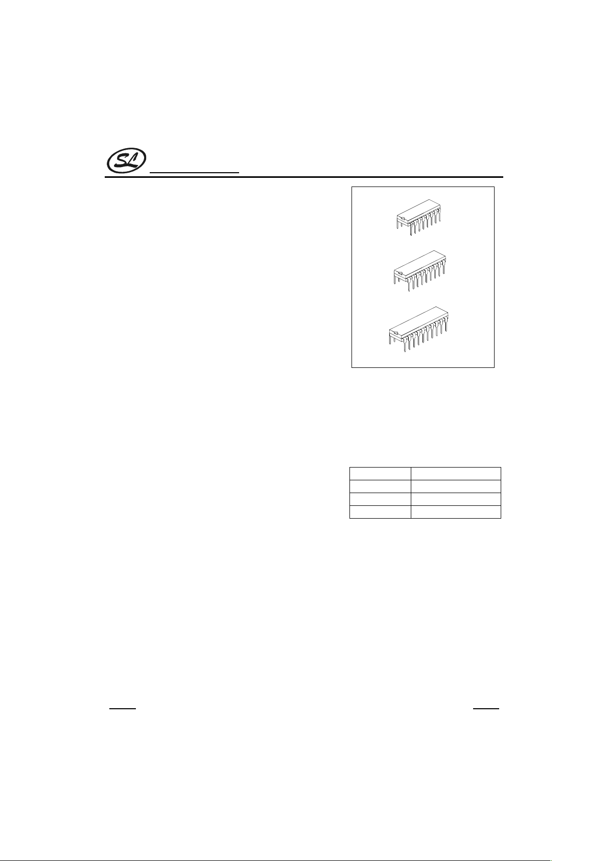
DIP-20
DIP-18
DIP-16
ORDERING INFORMATION
SC91214/15A DIP-16 Package
SC91214/15B DIP-18 Package
SC91214/15C DIP-18 Package
SC91214/15D DIP-20 Package
Page 2
Silan
Semiconductors
SC91214/15 SERIES
HANGZHOU SILAN MICROELECTRONICS JOINT-STOCK CO.,LTD
Rev: 1.0 2001.01.03
2
PIN CONFIGURATIONS
1
2
3
4
5
6
7
8 9
16
15
14
13
12
11
10
SC91214/15A
C3
C1
OSCI
OSCO
TONE
V
SS
R3
R2
R1
R4
DP
XMITMUTE
V
DD
MODE IN
C2
HK
a. DIP-16 Package
1
2
3
4
5
6
7
8
9
16
15
14
13
12
11
10
SC91214/15B
C3
C1
OSCI
OSCO
TONE
V
SS
R3
R2
R1
R4
DP
XMITMUT E
V
DD
MODE IN
C2
HK
b. DIP-18Package
(i) Key tone output
18
17
MODE OUT
KT
1
2
3
4
5
6
7
8
9
16
15
14
13
12
11
10
SC91214/15C
C3
C1
OSCI
OSCO
TONE
V
SS
R3
R2
R1
R4
DPXMITMUT E
V
DD
MODE IN
C2
HK
(ii) Hand-free control
18
17
HFO
HFI
1
2
3
4
5
6
7
8
9
16
15
14
13
12
1110
SC91214/15D
C3
C1
OSCI
OSCO
TONE
V
SS
R3
R2
R1
R4
DPXMITMUTE
V
DD
MODE IN
C2
HK
c. DIP-20 Package
20
19
18
17
HFO
MODE OUT
KT
HFI
Page 3
Silan
Semiconductors
SC91214/15 SERIES
HANGZHOU SILAN MICROELECTRONICS JOINT-STOCK CO.,LTD
Rev: 1.0 2001.01.03
3
BLOCK DIAGRAM
KEYBOARD
LOGIC
REDIAL MEMO RY
32 DIGITS
OUTPUT
LOGIC
DTMF
GENERATOR
INPUT LOGIC
CONTROL
LOGIC
OSC
R1
R4
C1
C3
MODE IN
HFI
HK
DP
KT
HFO
XMIT MUTE
MODE OUT
V
DD
TONE
OSCI
OSCO
ABSOLUTE MAXIMUM RATINGS
(Tamb=25°C, All voltage referenced to VSS, unless otherwise specified)
Characteristic Symbol Value Unit
Power Supply Voltage VDD 6.0 V
Input Voltage VIN -0.3~VDD+0.3 V
Output Voltage V
OUT
-0.3~VDD+0.3 V
Output Voltage (DP, XMIT MUTE) V
OUT
1.2 V
Tone Output Current I
TONE
50 mA
Power Dissipation PD 500 mW
Operating Temperature Topr -25~+70 °C
Storage Temperature Tstg -55~+150 °C
Note: Stresses above those listed under “Absolute Maximum Ratings” may cause permanent damage to this
device. These are stress ratings only. Functional operation of this device at these or any other conditions
above those indicated in the operational sections of this specification is not implied or intended. Exposure to
the absolute maximum rating conditions for extended periods may affect device reliability.
Page 4
Silan
Semiconductors
SC91214/15 SERIES
HANGZHOU SILAN MICROELECTRONICS JOINT-STOCK CO.,LTD
Rev: 1.0 2001.01.03
4
AC ELECTRICAL CHARACTERISTICS
(Top=25°C, VDD=3.5V, VSS=0V, fosc=3.579545MHz, All voltage referenced to V
SS,
unless otherwise specified)
Parameter Symbol Conditions Min Typ Max Unit
Tes t
KT.
Tone mode 2.0 -- 5.5
Operating Voltage VDD
Pulse mode 2.0 -- 5.5
V A
Memory Retention Voltage VMR 1 V --
Memory Retention Current IMR
V
DD
=1.0V, HK=VDD
All outputs unloaded
0.05 0.4 µA --
I
DDP
Pulse mode 0.32 1.0
Operating Current
I
DDT
Tone mode
All outputs unloaded
0.6 2.0
mA A
HK
=VDD=1.5V
0.03 0.05
Standby Current ISO
HK
=VSS
All outputs unloaded,
no key selected
0.5 10
µA A
VIH 0.8 1
Input Voltage
V
IL
0 0.2
V
DD
R1-R4
Input Current
I
R
115 µA C
VOC Column 584 730 876
Tone out Voltage
V
OR
Row
V
DD
=3.5V, RL=5K
456 570 684
mVp-p D
HFI
Pull Low Current
| I
HFI
|
V
DD
=3.5V (Note 1)
HFI
pin connected to 0V
5 µA B
HFO Drive Current | I
OH1
|
V
DD
=3.5V
V
OH=VDD
-0.4V
0.4 2 mA B
HFO, KT, MODEOUT
XMITMUTE
Sink Current
I
OL1
V
DD
=3.5V
V
OL
=0.4V
0.9 5.3 mA B
DP
Sink Current
I
OL2
VDD=3.5V, VOL=0.4V 1.1 5.3 mA B
Distortion DIS% * see note below 1 5 %
* Note:
1/2
22
1/2
222
)
V
IH
V
IL
(
)
V
n
V
2
V
1
( X 100
DIS%
+
+++
=
L
1. V
1
… Vn are the intermediation or the harmonic frequencies in the 500Hz to 3400Hz band.
2. V
IL
and VIH are the individual frequency components of the DTMF signal.
Page 5

Silan
Semiconductors
SC91214/15 SERIES
HANGZHOU SILAN MICROELECTRONICS JOINT-STOCK CO.,LTD
Rev: 1.0 2001.01.03
5
AC CHARACTERISTICS
(Top=25°C, VDD=3.5V, VSS=0V, fosc=3.579545MHz, All voltage referenced to V
SS,
unless otherwise specified)
Parameter Symbol Conditions Min Typ Max Unit
M/B=1/2 33.3
10pps
M/B=2/3 40.0
M/B=1/2 16.7
Make Time TM
20pps
M/B=2/3 20.0
ms
M/B=1/2 66.6
10pps
M/B=2/3 60.0
M/B=1/2 33.3
Break Time TB
20pps
M/B=2/3
30.0
ms
10pps 824
Inter-digit Pause Time T
IDP
20pps 458
ms
Pause Time T
PAU
2.2 sec
Auto-redial Break Time T
AOBK
2.2 sec
Delay Time Key Valid to Signal Out TD 0 ms
Key-in Debounce TKD 21 ms
Key Release Debounce Time T
KLD
5.2 ms
Key-in Tone Duration T
KTD
23 ms
Key-in Tone Frequency FKT 437 Hz
Minimum Tone Duration Time T
MFD
90 ms
Min. Tone Inter-digit Pause T
TIDP
100 ms
Redial Tone Duration T
MFDR
90 ms
Redial Tone Inter-digit Duration T
TIDPR
100 ms
COMPARISONS OF SPECIFIED VS ACTUAL TONE FREQUENCIES
(Fosc=3.579MHz)
R/C Spec. Actual Error (%) Unit
R1
697 699.1 +0.31 Hz
R2
770 771.5 +0.19 Hz
R3
852 852.3 +0.03 Hz
R4
941 942.0 +0.10 Hz
C1
1,29 1,215.7 +0.57 Hz
C2
1,336 1,331.7 -0.32 Hz
C3
1,477 1,471.9 -0.35 Hz
Page 6
Silan
Semiconductors
SC91214/15 SERIES
HANGZHOU SILAN MICROELECTRONICS JOINT-STOCK CO.,LTD
Rev: 1.0 2001.01.03
6
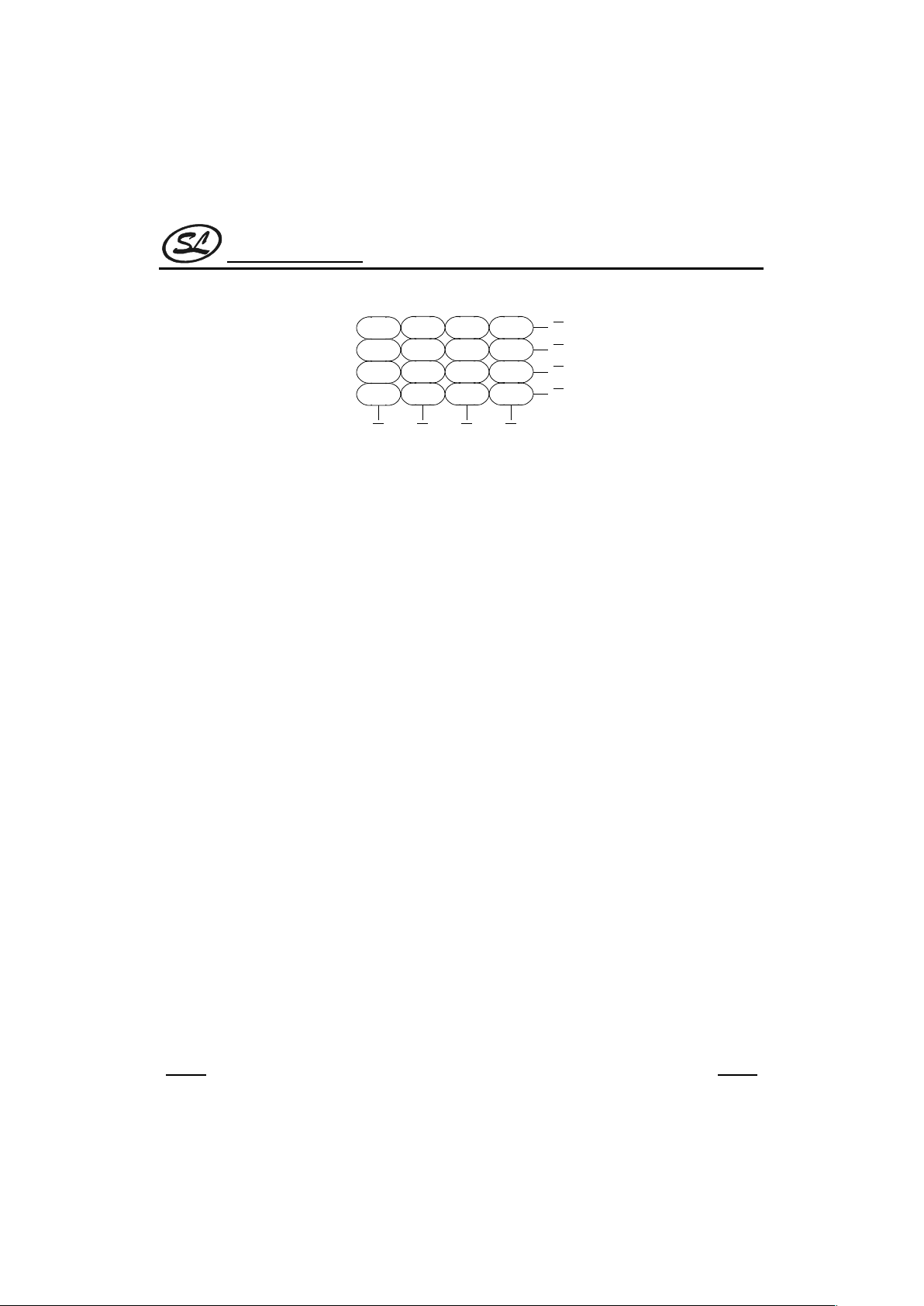
KEYBOARD ASSIGNMENT
1
23F1
4
56F2
7
89P
*/T
0#RD
C1 C2 C3 C4
R1
R2
R3
R4
1) */T: In PULSE mode this key works as Pulse→DTMF key (T key). In DTMF mode the key works as * key.
*/T key will occupy one memory digit in either use.
2) F1: Flash key. The break time is 297 ms or 96 ms (SC91214/15 respectively)
3) F2: Flash key for break time 640 ms
4) P: Pause key (2.2 seconds)
5) RD: One key redial key
6) EMn: One touch memory key
7) #: In PULSE mode this key input is neglected. In DTMF mode this key works as # key.
Page 7

Silan
Semiconductors
SC91214/15 SERIES
HANGZHOU SILAN MICROELECTRONICS JOINT-STOCK CO.,LTD
Rev: 1.0 2001.01.03
7
PIN DESCRIPTION
Pin No.
SC91214A SC91214B SC91214C SC91214D
Pin Name I/O Description
3
4
3
4
4
5
4
5
OSCI
OSCO
I Oscillator Input and Output pins.
The time base for the SC91214/15 is a
crystal controlled on-chip oscillator, which is
completed by connecting a 3.58MHz crystal
or ceramic resonator between the OSCI and
OSCO pins.
2 2 3 3 MODE IN I, Z TRI-STATE mode select pin.
There ate two versions of the SC91214/15
as follows:
a. SC91215 Series is for European and
American systems.
MODE
IN
Tone/
Pulse
Dial
Rate
M/B
Ratio
VDD Pulse 10pps 2/3
VSS Tone -- --
Floating Pulse 10pps 1/2
b. The SC91214 Series is for the Japanese
system.
MODE
IN
Tone/
Pulse
Dial
Rate
M/B
Ratio
VDD Pulse 10pps 1/2
VSS Tone -- --
Floating Pulse 20pps 1/2
The mode selection pin is checked for
tone/pulse dialing as each digit key entery.
In the PULSE mode, the dialing rate is
checked, along with the make/break ratio, at
first key entry.
1 1 2 2
HK
I Hook switch input
This inverter input pin detects the state of
the hook switch contact. “Off Hook” is
represented by a VDD condition.
(To be continued)
Page 8

Silan
Semiconductors
SC91214/15 SERIES
HANGZHOU SILAN MICROELECTRONICS JOINT-STOCK CO.,LTD
Rev: 1.0 2001.01.03
8
(Continued)
Pin No.
SC91214A SC91214B SC91214C SC91214D
Pin Name I/O Description
(N.A.) 10 (N.A.) 11
KT
O Key-in tone output
This N-channel open drain pin sends out a
“beep” tone for each PULSE mode key
entry, along with entries of accepted function
keys (RD, T, F1 F2, an P keys). The tone
output frequency is 437Hz and tone duration
is 23 ms.
9 11 10 12
DP
O Dialing pulse output
This is an N-channel open drain output. The
normal output will be “ON” during break an
“OFF” during make in the PULSE DIALING
mode.
1 1 HFO O (N.A.) (N.A.)
18 20
HFI
I
Hands-Free Control I/O pins
These pins enable and disable the
Hands-Free control function. When input pin
HFI
goes low, the Hands-Free Control
state is toggled on. The status of the
Hands-Free control state is listed in the
following table:
Current State Next State
HFO
Low
High
High
Low
High
HFO
High
Low
Low
Low
Low
High
Dialing?
Yes
No
Yes
Yes
No
Yes
Hook SW.
Off Hook
On Hook
Input
On Hook
On Hook
Off Hook
On Hook
Off Hook
-
Off Hook
HFI
HFI
HFI
(To be continued)
Page 9

Silan
Semiconductors
SC91214/15 SERIES
HANGZHOU SILAN MICROELECTRONICS JOINT-STOCK CO.,LTD
Rev: 1.0 2001.01.03
9
(Continued)
Pin No.
SC91214A SC91214B SC91214C SC91214D
Pin Name I/O Description
7 7 8 8 TONE O Tone dialing output
When a valid key-press is detected in the
DTMF mode, appropriate low group and
high group, frequencies the dual tone
output. TONE output is in the “OFF” state in
PULSE mode.
8 8 9 9
XMITMUTE
O Dialing transmission mute output
This is an N-channel open drain output. The
XMITMUTE
is normally “OFF”. During
pulse or DTMF dialing this output is “ON”.
(N.A.) 9 (N.A.) 10 MODE OUT O Mode output pin
This is an N-channel, open drain output. It is
“ON” during tone output and “OFF” during
pulse output.
13 15 14 16
R1
14 16 15 17
R2
15 17 16 18
R3
16 18 17 19
R4
10 12 11 13
C1
11 13 12 14
C2
12 14 13 15
C3
Keyboard pins
This input serves as the interface to an XY
matrix keyboard. On a 4 X 4 matrix
keyboard, the input from the fourth column,
C4
, should be connected to VSS.
6 6 7 7 VDD
5 5 6 6 VSS
Power supply pins
These devices are designed to operate from
2.0V to 5.5V.
Page 10

Silan
Semiconductors
SC91214/15 SERIES
HANGZHOU SILAN MICROELECTRONICS JOINT-STOCK CO.,LTD
Rev: 1.0 2001.01.03
10
KEYBOARD OPERATION
•
Symbol definitions:
In the description below, signals are defined in terms of the key or switch, which is activated.
OFF Hook
means the phone is off the hook.
ON Hook
means the phone is on the hook.
D1
represents for the first digit dialed in a string of digits.
Dn (Dk)
represents for the last digit dialed in a string of digits.
Dn+1
represent for the beginning of a new string of digits.
Dn+m
represents for the last digit in a new string of digits.
HFI
↓
represents for the switch that activates the HANDS-FREE DIALING mode going low.
*/T
is the Pulse-to-DTMF key.
RD
is the Redial key.
0
is the Zero key.
P
is the Pause key.
F
is the Flash key.
•
Recommended Operation
1. PULSE mode operation
a. Off Hook D1 … Dn
PULSE mode is defined as the INTIAL mode, provided the first keyboard input is not the */T key following
the Off Hook condition and the mode selection pin is floating (MODE IN = VDD or floating).
b. On Hook
HFI
↓ D1 … Dn
Pulse mode is defined as the INITIAL mode, provided the key input D1 is not */T while the mode
selection pin is VDD or floating. The chip will pause for 824 ms automatically after it detects an Off-Hook
condition or if the
HFI
↓ key is depressed. It then proceeds with pulse or DTMF dialing if any keys have
been depressed.
The dialing rate or make/break ratio is decided at the first key entry by checking the MODE IN status and
will not be altered. The MODE IN status can only switch the DIALING mode from PULSE to DTMF after the
first key ectry.
2. DTMF mode operation
a. Off Hook D1 … Dn or On Hook
HFI
↓ D1 … Dn
DTMF mode is defined as the INTIAL mode if the mode selection pin MOD IN is VSS.
Page 11

Silan
Semiconductors
SC91214/15 SERIES
HANGZHOU SILAN MICROELECTRONICS JOINT-STOCK CO.,LTD
Rev: 1.0 2001.01.03
11
b. Off Hook D1 … Dn or On Hook
HFI
↓ */T D1 … Dn
The INITIAL mode is PULSE mode if the mode selection pin, MODE IN, is VDD or floating. The */T key
can switch the DIALING mode to TONE mode. Unlike NORMAL mode switching, the */T key entry, as the
first key pressed, will not produce any pause time, there are only 31 digits of redial memory available in the
buffer to be used for operation a and b, since the mode switching key, */T, will occupy one digit of space.
3. Manual dialing with automatic access pause
a. Off Hook O P D1 … Dn
Pause key entries can be accepted and stored and stored in the redial memory. Each is stored as a digit.
Each key-in will provide a pause of 3.57 seconds, depending on which model is being used.
4. Redial
a. Off Hook RD or On Hook
HFI
↓ RD
Up to 32 digits (in PULSE mode) or 31 digits (in TONE mode) can be dialed using the RD key. The
RD key is disabled while PULSE or TONE signals are being transmitted. Redial will also be inhibited if the
last number dialed exceeds 32 digits because the redial memory can only hold 32 digits.
b. Off Hook RD D1 … Dn or On Hook
HFI
↓ RD D1 … Dn
After pressing the RD key, digits may be added to the number in redial memory. When finished dialing,
the redial memory will contain the original digits, plus the digits dialed after pressing RD . each time the
redial key is pressed, the stored number will be dialed exactly the same as it was previously, regardless of
the status of the MODE IN pin.
5. TONE/PULSE switch operation
a. Off Hook D1 … Dn MODE IN pin switched to VSS Dn+1 … Dn+m
PULSE Mode
DTMF Mode
The mode selection pin is always checked for TONE or PULSE mode key entry. Dialing can be switched
from PULSE to TONE mode, but not from TONE to PULSE mode. Switching the MODE IN pin to Vss will
cause the chip to store a */T digit prior to first tone digit in the redial memory and will automatically insert a
2.2 second pause before the tone digits are dialed out. After the mode has been switched, the status of the
mode selection pin will no longer be checked. Therefore, it will not be possible to switch from TONE to
PULSE mode.
Page 12

Silan
Semiconductors
SC91214/15 SERIES
HANGZHOU SILAN MICROELECTRONICS JOINT-STOCK CO.,LTD
Rev: 1.0 2001.01.03
12
b. Off Hook D1 … Dn */T Dn+1 … Dn+m
PULSE Mode DTMF MODE
PULSE mode is initially defined with the mode selection pin, MODE IN, equal to VDD or floating. At this
time, the mode can be switched to DTMF by pressing the */T key. DTMF mode will being as soon as the
last pulse has been transmitted. In this mode, Dn+1 through Dn+m are sent through the TONE OUT
pin as DTMF signals. If a P key entry is contained in the series of digits before or after the */T entry,
or the MODE IN switch is depressed, 2.2 second pause will be added to the automatically inserted pause
time, which is also 3.57 seconds. Both of the above switching modes can store as many as 31 digits in the
redial memory.
6. One-key redialing
Off-Hook D1 … Dn RD or On Hook
HFI
↓ D1 … Dn RD
If the dialing of D1 to Dn is finished, pressing RD will cause the pulse dialing pin to go low for 67
seconds of break time and an 824 ms pause will automatically be added. If the pulses of the number dialed
with D1 to Dn have not finished, the pressing of the redial key will be ignored.
7. Flash dialing
Off Hook F D1 … Dn or On Hook
HFI
↓ F D1 … Dn
The flash key emulate quick On-Off Hook operations. Pressing the flash keys, F1 or F2 , will cause a
break of 96 ms or 640 ms (or, 297 ms or 640 ms, depending on the mode) on the DP output pin. Then, it
pauses for 824 ms and continues dialing the digits, D1 to Dn . These digits are then stored in the redial
memory.
Each time the flash key is pressed, the redial memory will be cleared to store a new entry. In addition, the
MODE IN status will be checked again for the setting of the TONE/PULSE DIALING mode.
Similarly, to make sure that the IC is working properly, new flash key inputs will be ignored as long as the
digits that were dialed have not finished.
Page 13

Silan
Semiconductors
SC91214/15 SERIES
HANGZHOU SILAN MICROELECTRONICS JOINT-STOCK CO.,LTD
Rev: 1.0 2001.01.03
13
TEST CIRCUIT
A
Ic
Ic
VDD
VIN
R1 R2 R3 R4
C1 C2 C3 C4OR
VSS
(C)
(A)
KEYBOARD
T/P
A
VDD
VSS
HFI
MODE IN
(B)
A
V
MODE IN
VSS
HK
O/P
HK
VDD
KEYBOARD
T/P
VSS
VDD
HFI
HK
MODE IN
TONE
SPECTRUM ANALYZER
OSCILLOSCOPE
VDD
(D)
5K
OSCILLOSCOPE: TEKTRONI X 468
SPECTURM ANALYZER: HP3585A
Page 14

Silan
Semiconductors
SC91214/15 SERIES
HANGZHOU SILAN MICROELECTRONICS JOINT-STOCK CO.,LTD
Rev: 1.0 2001.01.03
14
TIMING DIAGRAMS
1.Timing diagram in PULSE mode:
TKD: debouncing time 21 ms
T
KTO
(23ms), f = 437Hz
Td T
IDP
T
M
T
M
21ms
T
M
T
B
Key Input
DP
XMIT MUTE
KT
HK or HFO
22 1 3
2. Timing diagram in TONE mode
(i) Normal dialing
T
KD
Td
2.3ms
Key Input
XMIT MUTE
KT
HK or HFO
MODE OUT
TONE
2.5ms 2.3m s 2. 3ms
T
MFD
: 94ms
T
TIDK
: 96ms
4 3 * 9
Page 15

Silan
Semiconductors
SC91214/15 SERIES
HANGZHOU SILAN MICROELECTRONICS JOINT-STOCK CO.,LTD
Rev: 1.0 2001.01.03
15
TIMING DIAGRAMS
(Continued)
(ii) After (i), redialing
Key Input
XMIT MUTE
KT
HK or HFO
MODE OUT
TONE
T
MFDR
T
TIDPR
Td
RD
2.3m s
3. Timing diagram for SWITCHING mode operation:
(i) By mode selection pin switches
Key Input
XMIT MUTE
KT
HK or HFO
MODE OUT
MODE IN
DP
T
M
T
IDP
T
M
T
IDP
T
d
T
MFD
T
PAU
2 3 */T 6 4
TONE
Page 16

Silan
Semiconductors
SC91214/15 SERIES
HANGZHOU SILAN MICROELECTRONICS JOINT-STOCK CO.,LTD
Rev: 1.0 2001.01.03
16
TIMING DIAGRAM
(Continued)
(ii) By */T key entry
Key Input
XMIT MUTE
KT
HK or HFO
MODE OUT
TONE
MODE IN
DP
T
M
T
IDP
T
M
T
d
T
MFD
T
PAU
2 3 */T
T
IDP
6 4
2.5ms 2.5ms
TPAU: Pause time (2.2 secs)
4. One key redial (DTMF mode used as example):
Key Input
XMIT MUTE
HK or HFO
MODE OUT
TONE
DP
2 3
2.5msT
d
T
d
2.5ms
T
AOBK
RD
TAOBK: Break time (2.2 secs)
Page 17

Silan
Semiconductors
SC91214/15 SERIES
HANGZHOU SILAN MICROELECTRONICS JOINT-STOCK CO.,LTD
Rev: 1.0 2001.01.03
17
TIMING DIAGRAM
(Continued)
5. Flash dialing (DTMF mode used as example):
Key Input
XMIT MUTE
HK or HFO
MODE OUT
TONE
DP
3
2.5ms
T
fsh
T
PAU
2.5ms
45F
Page 18

Silan
Semiconductors
SC91214/15 SERIES
HANGZHOU SILAN MICROELECTRONICS JOINT-STOCK CO.,LTD
Rev: 1.0 2001.01.03
18
TYPACAL APPLICATION CIRCUIT
47
3.9V
200
2M
8050
0.47
100k
0.02
VOICE
NETWORK
AMPLIFIER
NETWORK
1 2 3 F1
4 5 6 F2
7 8 9 P
* 0 # R
VDD
TIP
RING
OFF HOOK ON HOOK
470K
100K
220K
100K
100K
A92
A92
100K
A42
1K
22M
ON HOOK
OFF HOOK
HOOK SWITCH
0.47
470K
0.1
270K
100K
1K
8050
HANDS FREE
SPE
VDD
8050
100k
PIEZO
LED
100
M/B=2/3
M/B=1/2
PULSE TONE
20P
20P
3.58MHz
CERAMIC
RESONATOR
R1
R2
R3
R4
HFO
DP
HK
OSCO
HFI
TONE
KT
XMIT MUTE
MODE OUTMODE INVSSOSCI
C3
C2 C1
100K
V
DD
Page 19

Silan
Semiconductors
SC91214/15 SERIES
HANGZHOU SILAN MICROELECTRONICS JOINT-STOCK CO.,LTD
Rev: 1.0 2001.01.03
19
PACKAGE OUTLINE
DIP-16-300-2.54 UNIT:mm
6.40
2.54
3.51
5.083.30
7.62
0.25
15 degree
0.46
19.4
1.50
DIP-18-300-2.54 UNIT:mm
6.40
2.54
3.51
5.083.30
7.62
0.25
15 degree
0.46
22.95
1.50
Page 20

Silan
Semiconductors
SC91214/15 SERIES
HANGZHOU SILAN MICROELECTRONICS JOINT-STOCK CO.,LTD
Rev: 1.0 2001.01.03
20
PACKAGE OUTLINE
DIP-20-300-2.54 UNIT: mm
6.40
2.54
3.51
7.62
0.25
15 degree
0.46
22.95
1.50
5.083.30
 Loading...