

Page 1
Silan
Semiconductors
EXTENDED VOLTAGE CALLING
NUMBER IDENTIFICATION CIRCUIT 2
DESCRIPTION
The SC88E43 Calling Number Identification Circuit 2(ECNIC2) is
a low power CMOS integrated circuit intended for receiving physical
layer signals transmitted according to BT (British Telecom) SIN227
& SIN242, the U.K.’s CCA (Cable Communications Association)
TW/P&E/312 and Bellcore GR-30-CORE & SR-TSV-002476
specifications. The SC88E43 is suitable for applications using a
fixed voltage power source between 3 and 5V ±10%.
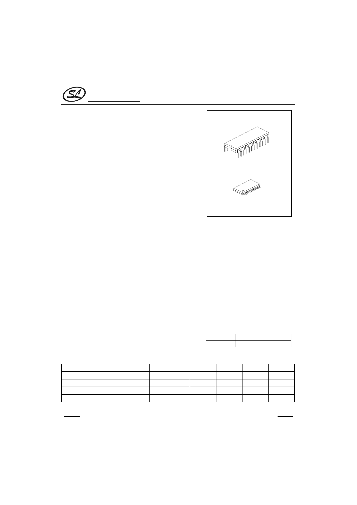
SC88E43
DIP-24
FEATURES
* Compatible with:
-- British Telecom (BT) SIN227 & SIN242
-- U.K.’s Cable Communications Association (CCA)
specification TW/P&E/312
-- Bellcore GR-30-CORE (formerly known as TR-NWT-000030)
& SR-TSV-002476
* Bellcore “CPE” Alerting Signal” (CAS) and BT “Idle State
Tone Alert Signal” detection
* Ring and line reversal detection
* 1200 baud Bell 202 and CCITT V.23 Frequency Shift Keying
(FSK) demodulation
* 3 or 5V ±10% supply voltage
* High input sensitivity (-40dBv Tone and FSK Detection)
* Selectable 3-wire FSK data interface
(microcontroller or SC88E43 controlled)
* Low power CMOS with powerdown mode
* Input gain adjustable amplifier
* Carrier detect status output
* Uses 3.58 MHz crystal
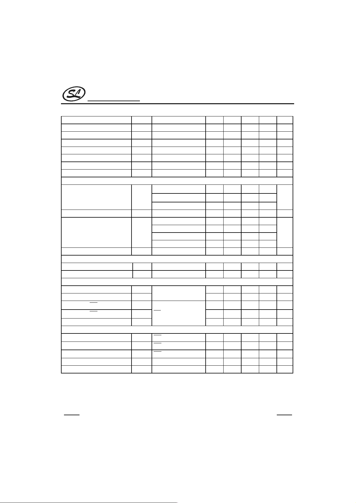
RECOMMENDED OPERATING CONDITIONS
Parameter Symbol Min Typ Max Unit
Power Supplies V
Clock Frequency f
Tolerance on Clock Frequency
Operating Temperature T
DD
OSC
∆f
C -0.1 -- +0.1 %
OP
SOP-24
APPLICATIONS
* BT Calling Line Identity Presentation
(CLIP), CCA CLIP, and Bellcore Calling
Identity Delivery (CID) systems
* Feature phones, including Analog
Display Services Interface (ADSI)
phones
* Phone set adjunct boxes
* FAX and answering machines
* Database query and Computer
Telephony Integration (CTI) systems
ORDERING INFORMATION
SC88E43
SC88E43S
(Ta=25°C ; Voltages are with respect to VSS)
2.7 -- 5.5 V
-- 3.579545 -- MHz
-40 -- 85
24 Pin DIP
24 Pin SOIC
°C
HANGZHOU SILAN MICROELECTRONICS JOINT-STOCK CO.,LTD
Rev: 1.0 2000.12.31
1
Page 2
Silan
Semiconductors
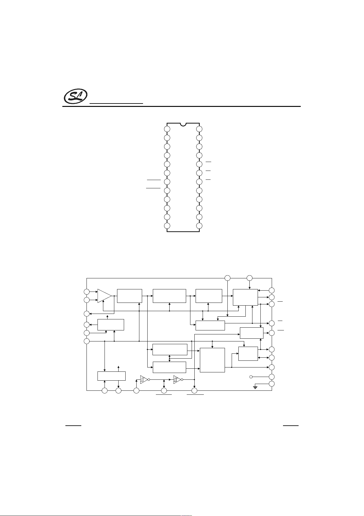
PIN CONFIGURATION
BLOCK DIAGRAM
TRIGin
TRIGRC
TRIGout
MODE
OSCO
IN+
IN-
GS
VRef
CAP
OSCI
Vss
1
2
3
4
5
6
7
8
9
10
11
12
SC88E43
SC88E43
VDD
24
23
St/GT
22
ESt
21
StD
20
INT
19
CD
18
DR
17
DATA
DCLK
16
FSKen
15
PWDN
14
IC
13
MODEFSKen
1
IN+
IN-
GS
VRef
CAP
PWDN
+
2
-
3
4
Generator
5
14
OSCin OSCout TRIGin
Anti-alias
Filter
To internal cct.
Bias
Alert Signal High
To internal cct.
Oscillator
10 11 6 7 8
Alert Signal Low
FSK Bandpass
Filter
Tone Filter
Tone Filter
TRIGRC
Demodulator
TRIGout
FSK
Carrier
Detector
Tone
Detection
Algorithm
Data
Timing
Recovery
Interrupt
Generator
Guard
Time
HANGZHOU SILAN MICROELECTRONICS JOINT-STOCK CO.,LTD
2
915
16
17
18
19
20
21
23
22
24
12
Rev: 1.0 2000.12.31
DCLK
DATA
DR
CD
INT
StD
St/GT
ESt
VDD
VSS
Page 3
Silan
Semiconductors
ABSOLUTE MAXIMUM RATINGS
Characteristic Symbol Value Unit
Supply Voltage V
Voltage on any pin other than supplies* V
Current at any pin other than supplies I
Storage Temperature Tstg -65 ~ +150
* Under normal operating conditions voltage on any pin except supplies can be minimum VSS -1V to
maximum V
DD +1V for an input current limited to less than 200mA.
(Voltages are with respect to VSS, unless otherwise stated).
DD
PIN
PIN
-0.3 ~ 6.0 V
Vss-0.3V ~ VDD+0.3V V
DC ELECTRICAL CHARACTERISTICS
Parameter Symbol Test conditions Min Typ Max Unit
All input are VDD/V
except for oscillator pins.
Stand-by Supply Current I
DDQ
No analog input.
Outputs unloaded.
PWDN = V
All input are VDD/V
Operating
Supply Current
VDD=5V±10%
V
=3V±10%
DD
except for oscillator pins.
No analog input.
I
DD
Outputs unloaded.
PWDN = V
FSKen = V
Power Consumption P
Schmitt Input High Threshold V
Schmitt Input Low Threshold V
Schmitt Hysteresis V
O
T+
T-
HYS
TRIGin,
TRIGin,
TRIGin,
TRIGRC
TRIGRC
TRIGRC
CMOS Input High Voltage VIHDCLK,MODE,FSKen Pins 0.7V
CMOS Input Low Voltage VILDCLK,MODE,FSKen Pins V
VOH=0.9V
Output High Sourcing Current I
OH
TRIGout
CD
,DCLK,DADA,
,StD,Est,St/GT Pins
VOL=0.1V
Output Low Sinking Current I
OL
TRIGout
CD
,DCLK,DATA,
, StD, Est,St/GT,
TRIGRC
VIN=VDDto V
I
IN1
Input Current
IN+,IN-,TRIGin Pins
VIN=VDDto V
I
IN2
PWDN,DCLK,MODE,FSKen
SS
-- 0.5 15
DD.
SS
-- 4.7 8 mA
SS;
DD.
-- 2.5 4.5 mA
-- -- -- 44 mW
DD
DD
INT
SS
SS
,PWDN Pins
,PWDN Pins
,PWDN Pins
Pins
DR
DR
0.48V
0.28V
0.2 -- -- V
,
0.8 -- -- mA
,
2----mA
-- -- 1
-- -- 10
SC88E43
10 mA
-- 0.68V
SS
DD
DD
DD
-- 0.48V
-- V
-- 0.3V
DD
DD
DD
DD
(To be continued)
°C
µA
V
V
V
V
µA
µA
HANGZHOU SILAN MICROELECTRONICS JOINT-STOCK CO.,LTD
Rev: 1.0 2000.12.31
3
Page 4
Silan
Semiconductors
(continued)
Parameter Symbol Test conditions Min Typ Max Unit
V
Output High-Impedance Current
Output Voltage V
Output Resistance R
Comparator Threshold Voltage V
=VDDto V
I
I
I
OUT
OZ1
TRIGRC
V
=VDDto V
OUT
OZ2
OZ3
REF
REF
TGt
Pin.
INT
V
=VDDto V
OUT
St/GT Pin.
No load.
Vref Pin
Vref Pin -- 2
St/GT Pin
Pin.
SS,
SS,
SS,
-- -- 1
-- -- 10
-- -- 5
0.5V
-0.05
0.5V
0.05
AC ELECTRICAL CHARACTERISTICS
Parameter Symbol Conditions Min Typ Max Unit Notes
Dual Tone Alert Signal Detection
Low Tone Frequency f
High Tone Frequency f
L
H
-- 2130 -- Hz
-- 2750 -- Hz
Frequency Deviation accept 1.1% -- -- -- 4
Frequency Deviation Reject 3.5% -- -- -- 5
Accept Signal Level Per Tone
Rejet Signal Level Per Tone
Positive And Negtive Twist
Accept
Signal to Noise Ratio SNR
TONE
Timming Parameter Measurement Voltage Levels
CMOS Threshold Voltage V
Rise/Fall Threshold Voltage High
Rise/Fall Threshold Voltage Low V
CT
V
HM
LM
-40 -- -2
-37.78 -- 0.22
-- -- -46 dBV
-- -- -43.78 dBm
7----
20 -- -- dB 1,2
-- 0.5V
-- 0.7V
-- 0.3V
Gain Setting Amplifier
Input Leakage Current I
IN
VSS≤ VIN≤ V
DD -- -- 1
Input Resistance RIN-- 10 -- -Input Offset Voltage V
Power Supply Rejection Ratio PSRR 1kHz ripple on V
-- -- -- 25 mV
OS
DD
40 -- -- dB
SC88E43
0.5V
--
0.5V
--
-- V
-- V
-- V
(To be continued)
DD
DD
-
DD
DD
DD
+0.05
+0.05
dBV
dBm
dB
µA
MΩ
DD
DD
a
b
c
µA
µA
µA
V
kΩ
V
3
3
HANGZHOU SILAN MICROELECTRONICS JOINT-STOCK CO.,LTD
Rev: 1.0 2000.12.31
4
Page 5
Silan
Semiconductors
(continued)
Parameter Symbol Conditions Min Typ Max Unit Notes
V
Common Mode Rejection CMRR
DC Open Loop Voltage Gain A
Unity Gain Bandwidth fC-- 0.3 -- -- MHz
Output Voltage Swing V
Maximum Capacitive Load (GS) CL-- -- -- 100 pF
Maximum Resistive Load (GS) RL-- 50 -- -Common Mode Range Voltage V
VOL
O
CM
≤ VIN≤ V
CMmin
-- 30 -- -- dB
Load ≥ 50kΩ
-- 1.0 -- VDD-0.1 V
CMmax 40 -- -- dB
0.5 -- V
FSK Detection
-- -40 -- -8
Input Detection Level
Transmission Rate -- 1188 1200 1212 baud
Input Frequency Detection
Signal to Noise Ratio SNR
-- -37.78 -- -5.78
-- 10 -- 398.1 mVrms
Bell 202 1 (Mark) 1188 1200 1212 Hz
Bell 202 0 (Space) 2178 2200 2222 Hz
CCITT V.23 1 (Mark) 1280.5 1300 1319.5 Hz
CCITT V.23 0 (Space) 2068.5 2100 2131.5 Hz
-- 20 -- -- dB 6,7
FSK
Dual Tone Alert Signal Timing
Alert Signal Present Detect Time t
Alert Signal Absent Detect Time t
-- 0.5 -- 10 ms 9
DP
-- 0.1 -- 8 ms 9
DA
3-Wire Interface Timming
Power-up Time t
Power-downTime t
Input FSK to
Input FSK to
Hysteresis
CD
CD
Low Delay
High Delay
PU
PWDN, OSC1 Pins
PD
t
CP
CD
t
CA
Pin
-- -- 50 ms
-- -- 1 ms
-- -- 25
8---8----ms
3-Wire Interface Timming (Mode 0)
RiseTime t
Fall Time t
Low Time
Rate -- DATA Pin 1188 1200 1212 baud 11
Input FSK to DATA delay t
RR DR
RF DR
tRL
IDD
Pin
Pin
Pin
DR
DATA Pin -- 1 5 ms
-- -- 200
-- -- 200
415 416 417
SC88E43
-0.5 V
DD
PP
kΩ
a
dBV
b
ms
ms
ns 10
ns 10
µs
6,8
12
dBm
(To be continued)
HANGZHOU SILAN MICROELECTRONICS JOINT-STOCK CO.,LTD
Rev: 1.0 2000.12.31
5
Page 6
Silan
Semiconductors
(continued)
Parameter Symbol Conditions Min Typ Max Unit Notes
Rise time t
Fall Time t
DATA to DCLK delay t
DCLK to DATA delay t
Frequency f
High Time t
Low Time t
DCLK to
DR
delay
R
F
DCD
CDD
DCLK0
CH
CL
t
CRD
DATA, DCLK Pins
DCLK Pin
DCLK ,
DR
Pin
3-Wire Interface Timming (Mode 1)
Frequency f
Duty Cycle 30 -- 70 %
RiseTime t
Rate t
Input FSK to DATA delay t
a. dBV= decibels above or below a reference voltage of 1Vrms. Signal level is per tone.
b. dBm = decibels above or below a reference power of 1mW into 600 ohms. 0dBm = 0.7746Vrms. Signal
level is per tone.
c. Twist = 20 log (f
H amplitude / fL amplitude).
DCLK1
R1
DDS
DDH
DCLK Pin
DCLK ,
DR
Pin
-- -- 200 ns 10
-- -- 200 ns 10
6 416 --
6 416 --
1201.6 1202.8 1204 Hz 12
415 416 417
415 416 417
415 416 417
-- -- 1 MHz
-- -- 20 ns
500 -- -- ns
500 -- -- ns
SC88E43
µs
µs
µs
µs
µs
11,12,
13
11,12,
13
12
12
12
Notes:
1. Both tones have the same amplitude.
2. Band limited random noise 300-3400Hz. Measurement valid only when tone is present.
3. With gain setting as shown in Figure 10. Production tested at V
DD =3V±10%, 5V±10%.
4. Range within which tones are accepted.
5. Ranges outside of which tones are rejected.
6. Both mark and space have the same amplitude.
7. Band limited random noise (200-3400Hz). Present when FSK signal is present. Note that the BT band is
300-3400Hz, the Bellcore band is 0-4kHz.
8. Production tested at V
DD =5V±10%, 3V±10%.
9. Refer to Figure 16 and 19.
10. into 50pF load.
11. FSK input data at 1200±12 baud.
12. OSCI at 3.579545 MHz±0.1%.
13. Function of signal condition.
HANGZHOU SILAN MICROELECTRONICS JOINT-STOCK CO.,LTD
Rev: 1.0 2000.12.31
6
Page 7
Silan
Semiconductors
PIN DESCRIPTION
Pin
No.
10 OSCI Input
11 OSCO Output
12 Vss -- Power Supply Ground.
13 IC -- Internal Connection. Must be connected to VSS for normal operation.
14 PWDN Schmitt Input
Symbol I/O Function
1 IN+ Input Non-inverting Input of the internal opamp.
2 IN- Input Inverting Input of the internal opamp.
Gain Select of internal opamp. The opamp’s gain should be set
3 GS Output
4VRef Output
5CAP --
6 TRIGin Trigger Input
TRIGRC
7
TRIGout
8
9 MODE CMOS Input
Open Drain
Output /
Schmitt Input
CMOS Output
according to the nominal Vdd of the application using the information
in Figure 10.
Reference Voltage. Nominally VDD/2. It is used to bias the input
opamp.
Capacitor. A 0.1mF decoupling capacitor should be connected across
this pin and V
Trigger Input. Schmitt trigger buffer input. Used for line reversal and
ring detection.
Trigger RC. Used to set the (RC) time interval from TRIGin going low
TRIGout going high. An external resistor connected to VDD and
to
capacitor connected to V
interval.
Trigger Out. Schmitt trigger buffer output. Used to indicate detection of
line reversal and/or ringing.
3-wire interface: Mode Select. When low, selects FSK data interface
mode 0. When high, selects FSK data interface mode 1. See pin 16
(DCLK) description to understand how MODE affects the DCLK pin.
Oscillator Input. A 3.579545MHz crystal should be connected between
this pin and OSCO. It may also be driven directly from an external
clock source.
Oscillator Output. A 3.579545MHz crystal should be connected
between this pin and OSCI. When OSCI is driven by an external clock,
this pin should be left open.
Power Down. Active high. When high, the device consumes minimal
power by disabling all functionality except TRIGin,
SS.
SS determine the duration of the (RC) time
TRIGout Must be pulled low for device operation.
HANGZHOU SILAN MICROELECTRONICS JOINT-STOCK CO.,LTD
7
SC88E43
TRIGRC and.
(To be continued)
Rev: 1.0 2000.12.31
Page 8
Silan
Semiconductors
(continued)
Pin
No.
15 FSKen CMOS Input
16 DCLK
17 DATA CMOS Output
18
19
20
21 StD CMOS Output
22 ESt CMOS Output
23 St/GT
24 VDD -- Positive Power Supply.
Symbol I/O Function
Input/Output
DR
CD
INT
CMOS Output
CMOS Output
Open Drain
Analog Input /
CMOS Output
CMOS
Output
FSK Enable. Must be high for FSK demodulation. This pin should be
set low to prevent the FSK demodulator from reacting to extraneous
signals (such as speech, alert signal and DTMF which are all in the
same frequency band as FSK).
3-wire Interface: Data Clock. In mode 0 (MODE pin low), this pin is an
output. In mode 1 (MODE pin high), this pin is an input.
3-wire Interface: Data. In mode 0 the FSK data appears at the pin
once demodulated. In mode 1 the FSK data is shifted out on the rising
edge of the microcontroller supplied DCLK.
3-wire Interface: Data Ready. Active low. In mode 0 this output goes
low after the last DCLK pulse of each data word. This identifies the 8bit word boundary on the serial output stream. Typically,
to latch 8-bit words from a serial-to-parallel converter into a
microcontroller. In mode 1 this pin will signal the availability of data.
Carrier Detect. Active low. A logic low indicates the presence of inband signal at the output of the FSK bandpass filter.
Interrupt. Active low. It is active when
StD is high. This output stays low until all three signals have become
inactive.
Dual Tone Alert Signal Delayed Steering Output. When high, it
indicates that a guard time qualified alert signal has been detected.
Dual Tone Alert Signal Early Steering Output. Alert signal detection
output. Used in conjunction with St/GT and external circuitry to
implement the detect and non-detect guard times.
Dual Tone Alert Signal Steering Input/Guard Time. A voltage greater
than V
TGt (see figure 4) at the St/GT pin causes the device to indicate
that a dual tone has been detected by asserting StD high. A voltage
less than V
TGt frees the device to accept a new dual tone.
SC88E43
DR is used
TRIGout or DR is low, or
HANGZHOU SILAN MICROELECTRONICS JOINT-STOCK CO.,LTD
Rev: 1.0 2000.12.31
8
Page 9

Silan
Semiconductors
FUNCTIONAL DESCRIPTION
Detection of CLIP/CID Call Arrival Indicators
The cricuit in Figure 3 illustrates the relationship between the TRIGRC and TRIGout sig nals.Tpically,the three
pin combination is used to detect an event indicated by an increase of the TRIGin voltage from V
Schmitt trigger high going threshold V
Figure 3 shows a circuit to detect any one of three CLIP/CID call arrival indicators:line reversal,ring burst and
ringing.
C1=100nF
Tip/A
T+ (see DC electrical characteristics).
R1=499kΩ
V1
V3
R3=200kΩ
TRIGin
SC88E43
SC88E43
max VT+=0.68 V
min VT+=0.48 V
ss to above the
V
DD
DD
DD
Ring/B
Notes:
The application circuit must ensure rhat, V
Where max VT+=3.74V @VDD=5.5V.
Tolerance to noise between A/B and V
max Vnoise=(minV
Suggested R5C3 component values:
R5 from 10kΩ to 500kΩ; C3 from 47nF to 0.68µF
An example is C3=220nF, R5=150kΩ; TRIGout low from
21.6ms to 37.6ms after TRIGin Signal stops triggering the
circuit.
C2=100nF
R2=499kΩ
TRIGin
is:
)/0.30+0.7=5.6Vrms@4.5VV
T+
SS
V4
>max V
DD
T+
R4=310kΩ
R5=150kΩ
C3=220nF
To Microcontroller
TRIGRC
TRIGout
To determine values for C3 and R5:
R5C3=-t/ln(1-V
TRIGRC/VDD
)
Figure 3 Circuit to Detect Line Reversal, Ring Burst and Ringing
1.Line Reversal Detection
Line reversal,or polarity reversal on the A and B wires indicates the arrival of an inconming CDScall,as soecified in
SIN227.When the event (line reversal) occurs,TRIGin rises past the high going Schmitt threshold V
T+ and
tTRIGou ,which is normally high,is pulled low going Schmitt threshold VT- and TRIGout returns high.The
components R5 and C3 (see Figure 3) at
In a TE designed for CLIP,the
TRIGout high to low transition may be used to interrupt or wake-up the micro-
TRIGout low interval.
controller.The controller can thus be put into power-downmode to conserve power in a battery operater TE.
2.Ring Buost Detection
CCA doesnot support the dual tone alert signal (refer to Dual Tone Alert single burst og ringing (duration 200450ms) that precedes CLIPFSK data.The ring burst may vary fron 30 to 75Vrms and is approximately 25Hz.
Again in aTEdesigned for CCA CLIP ,the
microcontroller.The controller can thus be put into power-down mode to conserve powerin a battery operated TE.
tTRIGou high to low reansition may be used to interrupt or wake-up the
HANGZHOU SILAN MICROELECTRONICS JOINT-STOCK CO.,LTD
Rev: 1.0 2000.12.31
9
Page 10

Silan
Semiconductors
3.Ring Detection
In Bellcore’s CND/CNAM scheme, the CID FSK data is transmitted between the first and second ringing cycles.
The circuit in Figure 3 will generate a ring envelope signal (active low) at
40Vrms. R5 and C3 filter the ring signal to provide an envelope output.
The diode bridge shown in Figure 3 works for both single ended and balanced ringing. A fraction of the ring
voltage is applied to the TRIGin input. When the voltage at TRIGin is above the Schmitt trigger high going
threshold V
the minimum V
In a CPE designed for CND/CNAM, the
microcontroller. The controller can thus be put into power down mode to conserve power.
If precise ring duration determination is critical, capacitor C3 in Figure 3 may be removed. The microcontroller
will now be able to time the ring duration directly. The result will be that
ringing signal is present.Previously the RC time constant would cause only one interrupt.
Dual Tone Alert Signal Detection
The BT on hook (idle state) caller ID scheme uses a dual tone alert signal whose characteristics are shown in
Table 1.
Bellcore specifications for a similar dual tone signal called CPE Alerting Signal (CAS) for use in off-hook data
transmission. For the CIDCW service, the CAS must be detected in the presence of near end speech. The CAS
detector must also be immune to imitation from near and farend speech.
T+ , TRIGRC is pulled low as C3 discharges. TRIGout stays low as long as the C3 voltage stays below
T+ .
TRIGout high to low transition may be used to interrupt or wake up the
TRIGout for a ring voltage of at least
TRIGout w ill be low only as long as the
SC88E43
Item BT Bellcore
Low tone frequency
High tone frequency
Received signal level
Signal reject level -46dBV (-43.78dBm) -45dBm
Signal level differntial (twist) Up to 7dB Up to 6dB
Unwanted signals
Duration
Speech present No Yes
a. In the future BT may specify the off-hook signal level as –15dBm to –34dBm per tone for BT CIDcw.
b. The signal power is expressed in dBm referenced to 600 ohm at the CPE A/B (tip/ring) interface.
c. ASL = active speech level expressed in dBm referenced to 600 ohm at the CPE tip/ring interface. The level is measured
according to method B of Recommendation P.56 "Objective Measurement of Active Speech Level" published in the CCITT
Blue Book, volume V "Telephone Transmission Quality" 1989. EPL (Equivalent Peak Level) = ASL+11.7dB.
d. SIN227 suggests that the recognition time should be not less than 20ms if both tonesare detected.
hook
Table 1 Dual Tone Alert Signal Characteristics
2130Hz ± 1.1% 2130Hz ± 0.5%
2750Hz ± 1.1% 2750Hz ± 0.5%
-2dBV to –40dBV per tone on-
a
(0.22dBmbto –37.78dBm)
≤-20dB(300-3400Hz)
88ms to 110ms
d
-14dBm
≤–7dBm ASL
b
to –32dBm per tone
on-hook
c
near end
speech
75ms to 85ms
HANGZHOU SILAN MICROELECTRONICS JOINT-STOCK CO.,LTD
Rev: 1.0 2000.12.31
10
Page 11

Silan
Semiconductors
In the SC88E43 the dual tone signal is separated into a high and a low tone by two bandpass filters. A detection
algorithm examines the two filter outputs to determine the presence of a dual tone alert signal. The ESt pin goes
high when both tones are present. Note that ESt is only a preliminary indication. The indication must be sustained
over the tone present guard time to be considered valid. Tone present and tone absent guard times can be
implemented with external RC components. The tone present guard time rejects signals of insufficient duration.
The tone absent guard time masks momentary detection dropout once the tone present guard time has been
satisfied. StD is the guard time qualified detector output.
Dual Tone Detection Guard Time
When the dual tone signal is detected by the SC88E43, ESt goes high. When the signal ceases to be detected,
ESt goes low.
The ESt pin indicates raw detection of the dual tone signal. Since the BT application requires a minimum signal
duration and the Bellcore application requires protection from imitation by speech, Est detection must be guard
time qualified. The StD pin provides guard time qualified signal detection. When the SC88E43 is used in a caller
identity system, StD indicates correct CAS/Tone Alert Signal detection.
SC88E43
Tone detected
VDD
Figure 4 : Guard Time Circuit Operation
SC88E43
From
detector
Comparator
The total recognition time is t
PNQ1
+
-
V
TGt
Q2
=VSS
REC =tGP +tDP , where tGP is the tone present guard time and tDP is the tone
St/GT
ESt
StD
C
Figure 4 shows the relationship between the
St/GT, ESt and StD pins. It also shows the
R
SW1
A
B
VSS
operation of the guard time circuit.
present detect time (refer to timing between ESt, St/GT and StD in Figures 17 and 20).
The total tone absent time is t
ABS =tGA +tDA , where tGA is the tone absent guard time and tDA is the tone
absent detect time (refer to timing between ESt, St/GT and StD in Figures 17 and 20).
Bellcore states that it is desirable to be able to turn off CAS detection for an off-hook capable CPE. The disable
switch allows the subscriber who disconnects a service that relies on CAS detection (e.g., CIDCW) but retains the
CPE, to turn off the detector and not be bothered by false detection.
When SW1 in Figure 4 is in the B position the guard time circuit is disabled. The detector will still process
CAS/Alerting tones but the SC88E43 will not signal their presence by ensuring that StD is low.
BT specifies that the idle state tone alert signal recognition time should not be less than 20ms when both tones are
used for detection. That is, both tones must be detected together for at least 20ms before the signal can be
declared valid. This requirement can be met by setting the t
GP (refer to Figure 5) to at least 20ms.
HANGZHOU SILAN MICROELECTRONICS JOINT-STOCK CO.,LTD
Rev: 1.0 2000.12.31
11
Page 12

Silan
Semiconductors
BT also specifies that the TE is required to apply a DC wetting pulse and an AC load 15-25ms after the end of the
alerting signal. If t
at the falling edge of StD. The maximum t
than t
GA . Figure 5(a) shows a possible implementation. The values in Figures 9 and 11 (R2=R3=422K, C=0.1mF)
will meet the BT timing requirements.
ABS =tDA +tGA is 15 to 25ms, the DC current wetting pulse and the AC load can both be applied
DA is 8ms so tGA should be 15-17ms. Therefore, tGP must be greater
SC88E43
SC88E43
V
DD
St/GT
ESt
(a) tGP>t
GA
tGP=R1Cln[VDD/(VDD-VTG)]
t
=RpCln[(VDD-VD(Rp/R2))/(V
GA
Rp=R1R2/(R1+R2)
24
C
23
22
VD=diode forward voltage
R1
(Rp/R2))]
TGt-VD
R2
(b) tGP<t
tGP=RpCln[(VDD-VD(Rp/R2))/(VDD-V
t
GA
Rp=R1R2/(R1+R2)
SC88E43
St/GT
GA
=R1Cln[VDD/VTG)]
V
ESt
24
DD
C
23
22
VD=diode forward voltage
R1
TGt-VD
R2
(Rp/R2))]
Figure 5 Guard Time Circuits With Unequal Times
Input Configuration
The SC88E43 provides an input arrangement comprised of an operational amplifier, and a bias source (Vref )
which is used to bias the opamp inputs at V
DD/2. The feedback resistor at the opamp output (GS) can be used to
adjust the gain. In a single-ended configuration, the opamp is connected as shown in Figure 6. For a differential
input configuration, Figure 7 shows the necessary connections.
IN+
1
IN-
2
CR
Voltage Gain
(A
)=RF/R
V
IN
R
IN
GS
3
F
4
V
Ref
Figure 6 Single Ended Input Configuration
CR
1
R
C
4
R
5
R
R
Differental Input Amplifler
C1=C2
R1R4 (For unity gain R5=R4)
R3=(R2R5)/(R2+R5)
Voltage Gain
(AVdiff)=R5/R1 (see Figure 9,10,11)
Input Impedance
(ZINdiff)=2R1
2
+(1/C)
2
2
3
Figure 7 Differential Input Configuration
IN+
1
IN-
2
GS
3
4
V
Ref
HANGZHOU SILAN MICROELECTRONICS JOINT-STOCK CO.,LTD
Rev: 1.0 2000.12.31
12
Page 13

Silan
Semiconductors
FSK Demodulation
The SC88E43 first bandpass filters and then demodulates the FSK signal. The carrier detector provides an
indication of the presence of signal at the bandpass filter output. The SC88E43’s dual mode 3-wire interface allows
convenient extraction of the 8-bit data words in the demodulated FSK bit stream.
Note that signals such as CAS/Tone Alert Signal, speech and DTMF tones lie in the same frequency band as
FSK. They will, therefore, be demodulated and as a result, false data will be generated. To avoid demodulation of
false data, an FSKen pin is provided so that the FSK demodulator may be disabled when FSK signal is not
expected. There are two events that if either is true, should be used to disable FSKen. The events are
returning high or receiving all the data indicated by the message length word.
Item BT Bellcore
Mark frequency (logic 1)
Space frequency (logic 0)
Received signal level-mark
Received signal level-space -8dBV to –40dBV -12dBm to –36dBm
Signal level differntial (twist) Up to 6dB
Unwanted signals
Transmission rate
Word formate
1 start bit (logic 0), 8 bit word (LNB
1300Hz ± 1.5% 1200Hz ± 1%
2100Hz ± 1.5% 2200Hz ± 1%
-8dBV to –40dBV
(-5.78dBm to –37.78dBm)
≤-20dB (300-3400Hz)
1200baud ± 1% 1200baud ± 1%
first), 1 to 10 stop bits (logic 1)
Table 2 FSK Charateristics
SC88E43
a
-12dBm
≤–25dBm (0-4kHz)
1 start bit (logic 0), 8 bit word
(LNB first), 1 stop bits (logic 1)
to –32dBm
Up to 10dB
b
c
CD
a.The signal power is expressed in aBm referenced to 600Ω at the CPE tip/ring (A/B) interface.
b.SR-3004, Issue 2, January 1995.
c.The frequency rangeis specified in GR-30-CORE.
d.Up to 20 marks may be inserted in specific places in a single or multiple data message.
The FSK characteristics described in Table 2 shows the BT and Bellcore specifications. The BT frequencies
correspond to CCITT v.23. The Bellcore frequencies correspond to Bell 202. The U.K.’s CCA requires that the TE
be able to receive both CCITT v.23 and Bell 202 formats. The SC88E43 is compatible with both formats without
any adjustment.
3-wire FSK Data Interface
The SC88E43 provides a powerful dual mode 3-wire interface so that the 8-bit data words in the demodulated
FSK bit stream can be extracted without the need either for an external UART or for the TE/CPE’s microcontroller
to perform the UART function in software. The interface is specifically designed for the 1200 baud rate and is
comprised of the DATA, DCLK (data clock) and
via control of the device’s MODE pin: in mode 0, data transfer is initiated by the SC88E43; in mode 1, data transfer
is initiated by the external microcontroller.
DR (data ready) pins. Two modes (modes 0 and 1) are selectable
HANGZHOU SILAN MICROELECTRONICS JOINT-STOCK CO.,LTD
Rev: 1.0 2000.12.31
13
Page 14

Silan
Semiconductors
Mode 0
This mode is selected when the MODE pin is low.
In this mode, The SC88E43 receives the FSK signal, demodulates it, and outputs the data directly to the DATA
pin (refer to Figure 14). For each received stop and start bit sequence, the SC88E43 outputs a fixed frequency
clock string of 8 pulses at the DCLK pin. Each clock rising edge occurs in the centre of each DATA bit cell. DCLK is
not generated for the stop and start bits. Consequently, DCLK will clock only valid data into a peripheral device
such as a serial to parallel shift register or a micro-controller. The SC88E43 also outputs an end of word pulse
(data ready) on the
stop bits) sent from the network to the TE/CPE. This
can also cause a serial to parallel converter to parallel load its data into a microcontroller. The mode 0 data pin can
also be connected to a personal computer’s serial communication port after converting from CMOS to RS-232
voltage levels.
DR pin. The data ready signal indicates the reception of every 10-bit word (including start and
DR signal can be used to interrupt a micro-controller. DR
Mode 1
This mode is selected when the MODE pin is high. In this mode, the microcontroller supplies read pulses (DCLK)
to shift the 8-bit data words out of the SC88E43, onto the DATA pin. The SC88E43 asserts
boundary and indicate to the microprocessor that a new word has become available (refer to Figure 16).
Internal to the SC88E43, the demodulated data bits are sampled and stored. After the 8th bit, the word is parallel
loaded into an 8 bit shift register and
the supplied DCLK’s rising edge in the order they were received.
If DCLK begins while
interrupt (see section on "Interrupt") to be cleared by the first read pulse. Otherwise DR is low for half a nominal bit
time (1/2400 sec).
DR is low, DR will return to high upon the first DCLK. This feature allows the associated
DR goes low. The shift register’s contents are shifted out to the DATA pin on
SC88E43
DR to denote the word
After the last bit has been read, additional DCLKs are ignored.
Carrier Detector
The carrier detector provides an indication of the presence of a signal in the FSK frequency band. It detects the
presence of a signal of sufficient amplitude at the output of the FSK bandpass filter. The signal is qualified by a
digital algorithm before the
allow for momentary signal drop out once
FSK bandpass filter output for 8 ms.
When
CD is inactive (high), the raw output of the demodulator is ignored by the data timing recovery circuit
(refer to Figure 1). In mode 0, the DATA pin is forced high. No DCLK or
internal shift register is not updated. No
Note that signals such as CAS/Tone Alert Signal, speech and DTMF tones also lie in the FSK frequency band
and the carrier detector may be activated by these signals. The signals will be demodulated and presented as data.
To avoid false data detection, the FSKen pin should be used to disable the FSK demodulator when no FSK signal
is expected.
Ringing, on the other hand, does not pose a problem as it is ignored by the carrier detector.
CD output is set low to indicate carrier detection. An 8ms hysteresis is provided to
CD has been activated. CD is released when there is no activity at the
DR signal is generated. In mode 1, the
DR is generated. If the mode 1 DCLK is clocked, DATA is undefined.
HANGZHOU SILAN MICROELECTRONICS JOINT-STOCK CO.,LTD
Rev: 1.0 2000.12.31
14
Page 15

Silan
Semiconductors
Interrupt
To facilitate interfacing with microcontrollers running interrupt driven firmware, an open drain interrupt output
INT is provided. INT is asserted when TRIGout is low, StD is high, or DR is low. When INT is asserted, these
signals should be read (into an input port of the microcontroller) to determine the cause of the interrupt (
StD or
DR ) so that the appropriate response can be made.
When system power is first applied,
no initial charge. This will result in an interrupt upon power up. Also when system power is first applied and the
PWDN pin is low, an interrupt will occur due to StD. Since there is no charge across the capacitor at the St/GT pin
in Figure 4, StD will be high triggering an interrupt. The interrupts will not clear until both capacitors are charged.
The microcontroller should ignore interrupt from these msources on initial power up until there is sufficient time to
charge the capacitors.
It is possible to clear StD and its interrupt by asserting PWDN immediately after system power up. When PWDN
is high, StD is low. PWDN will also force both ESt and the comparator output low, Q2 will turn on so that the
capacitor at the St/GT pin charges up quickly (refer to Figure 4).
Power Down Mode
For applications requiring reduced power consumption, the SC88E43 can be powered up only when it is required,
that is, upon detection of one of three CLIP/CID call arrival indicators: line reversal, ring burst and ringing.
The SC88E43 is powered down by setting the PWDN pin to logic high. In power down mode, the oscillator, input
opamp and all internal circuitry are disabled except for TRIGin,
not affected by power down, such that, the SC88E43 can still react to call arrival indicators. The SC88E43 can be
powered up by setting the PWDN pin to logic low.
Crystal Oscillator
The SC88E43 requires a 3.579545MHz crystal oscillator as the master timing source.
TRIGout will be low because capacitor C3 at TRIGRC (see Figure 3) has
TRIGRC and tTRIGou pins. These three pins are
SC88E43
TRIGout ,
The crystal specification is as follows :
SC88E43
OSCI OSCO
10 11
3.579545 MHz
Figure 8 Common Crystal Connection
Any number of SC88E43 devices can be connected as shown in Figure 8 such that only one crystal is required.
The connection between OSC2 and OSC1 can be DC coupled as shown, or the OSC1 input on all devices can be
driven from a CMOS buffer (dc coupled) with the OSC2 outputs left unconnected.
To meet BT and Bellcore requirements for proper tone detection the crystal must have a frequency tolerance of
0.1%.
SC88E43
OSCI
10 11
OSCO
SC88E43
OSCI OSCO
10 11
to the next
SC88E43
Frequency: 3.579545 MHz
Frequency tolerance: ±0.1%(-40 o C+85 o
C)
Resonance mode: Parallel
Load capacitance: 18 pF
Maximum series resistance: 150 ohms
Maximum drive level (mW ): 2 mW
HANGZHOU SILAN MICROELECTRONICS JOINT-STOCK CO.,LTD
Rev: 1.0 2000.12.31
15
Page 16

Silan
Semiconductors
VRef and CAP Inputs
VRef is the output of a low impedance voltage source equal to VDD /2 and is used to bias the input opamp. A
0.1mF capacitor is required between CAP and V
SS to eliminate noise on VRef.
SC88E43
DD
V
TIP /A
RING / B
TISP
4180
22nF
5%
22nF
5%
100nF 5%
1N914 x 4
100nF 5%
R1
R1
499K 5%
499K 5%
1N4003
1N4003
1N4003
1N4003
301K
5%
R4
V
DD
R4
V
V
150K 5%
200K 5%
220nF 100nF
IN+
1
IN-
2
464K
GS
53K6
60K4
464K
DD
DD
3
Vref
4
CAP
5
TRIGin CD
6
7
TRIGout
8
MODE
9
OSCin
10
OSCout
11
V
SS
12
V
St/GT
ESt
StD
INT
DRTRIGRC
DATA
DCLK
FSKen
PWDN
DD
24
23
R3
22
R2
21
20
19
18
17
16
15
14
IC
13
SC88E43
Note:Resistors must have 1% tolerance and capacitors have 20% tolerance unless otherwise specified.
Crystal is 3.579545MHz, 0.1% frequency tolerance.
For BTApplicationC=0.1F5%, R3=422k1%, R2=422k1%.
For Applications where CAS speech immunity is required(e.g.CIDCW), C=0.1F5%, R3=825k1%, R2=226k
1%.
R1=430k, R4=34k for VDD=5V10% (See Figure 10)
R1=620k, R4=63k4 for VDD=3V10% (See Figure 10)
1N914
DD
V
100nF
C
100K
20%
V
DD
Figure 9- Application Circuit
Application Circuits
The circuits shown in Figures 9 and 11 are application circuits for the SC88E43. As supply voltage (VDD ) is
decreased, the threshold of the device’s tone and FSK detectors will be reduced. Therefore, to meet the BT or
Bellcore tone reject level requirements the gain of the input opamp should be reduced according to the graph in
HANGZHOU SILAN MICROELECTRONICS JOINT-STOCK CO.,LTD
Rev: 1.0 2000.12.31
16
Page 17

Silan
Semiconductors
Figure 10. For example when VDD =5V (+/- 10%), R 1 should equal 430kW and R4 should equal 34kW; and if VDD
=3V (+/- 10%) R1 should equal 620kW and R 4 should equal 63.4kW. Resistors R1 and R4 are shown in Figures 9
and 11.
The circuit shown in Figure 9 illustrates the use of the SC88E43 in a proprietary system that doesn’t need to
meet FCC, DOC, and UL approvals. It should be noted that if glitches on the Tip/Ring interface are of sufficient
amplitude, the circuit will falsely detect these signals as ringing or line reversal.
The circuit shown in Figure 11 will provide common mode rejection of signals received by the ringing circuit. This
circuit should pass safety related tests specified by FCC Part 68, DOC CS-03, UL 1459, and CSA C22.2. These
safety tests will simulate high voltage faults that may occur on the line. The circuit provides isolation from these
high voltage faults via R1 and the 12.1kWresistors as well as the 22nF & 330nF capacitors. IRC manufactures a
resistor (part number GS3) that should be used for R1. This resistor is a 3W, 5%, 1kV power resistor. The 12k1
resistor is manufactured by IRC (part number FA8425F). This resistor is a 1.5W, 5%, fuseable type resistor. The
22nF and 330nF capacitors have a 400V rating.
1
0.95
0.9
SC88E43
0.85
0.8
0.75
Gain Ratio
0.7
0.678
0.65
0.6
22.533.544.555.56
Nominal VDD(Volts)
Figure 10: Gain Ratio as a function of Nominal VDD
Note: In the application circuits shown in Figure9 and 11, the Gain ratio of SC88E43 opamp is:
Gain Ratio=464k/(R1+R4)
HANGZHOU SILAN MICROELECTRONICS JOINT-STOCK CO.,LTD
17
Rev: 1.0 2000.12.31
Page 18

Silan
Semiconductors
SC88E43
DD
V
TIP /A
RING / B
330nF
10%
TISP
4180
100nF
12K1
5%
V
10%
22nF
5%
22nF
5%
4N25
DD
1N4003
R1
1N4003
R1
1N4003
464K
5%
1N4003
1N914 X 4
200K
R4
V
DD
53K6
60K4
R4
V
DD
V
DD
1N5231B
150K 5%
5%
10nF
220nF
100nF
464K
IN+
1
IN-
2
GS
3
Vref
4
CAP
5
TRIGin CD
6
7
TRIGout
8
MODE
9
OSCin
10
OSCout
11
V
SS
12
V
St/GT
ESt
StD
INT
DRTRIGRC
DATA
DCLK
FSKen
PWDN
DD
24
23
R3
22
R2
21
20
19
18
17
16
15
14
IC
13
SC88E43
Note: Please use 0.068µF, 1500pF Mylar Capacitors.
Note:Resistors must have 1% tolerance and capacitors have 20% tolerance unless otherwise specified.
Crystal is 3.579545MHz, 0.1% frequency tolerance.
For BTApplicationC=0.1F5%, R3=422k1%, R2=422k1%.
For Applications where CAS speech immunity is required(e.g.CIDCW), C=0.1F5%, R3=825k1%, R2=226k
1%.
R1=430k, R4=34k for VDD=5V10% (See Figure 10)
R1=620k, R4=63k4 for VDD=3V10% (See Figure 10)
1N914
DD
V
100nF
C
V
100K
20%
DD
Figure 11:Application Circuit with Improved Common Mode Noise Immunity and Isolation in Line Interface
Approvals
Fcc Part 68,DOC CS-03,UL1459,and CAN/CSA-22.2 No.225-M90 are all system(i.e. connectors,power
supply,cabinet,ect.) requirements. Since the SC88E43 is a component and not a system, the application circuit
(Figure 11) has been designed to meet the CO Trunk interface requirments of FCC,DOC,UL, and CSA; thus
enabling the complete system to be approved by these standards bodies.
HANGZHOU SILAN MICROELECTRONICS JOINT-STOCK CO.,LTD
Rev: 1.0 2000.12.31
18
Page 19

Silan
Semiconductors
t
t
DCD
CDD
DATA
t
t
R
F
DCLK
t
t
CL
t
R
CH
Figure 12: DATA and DCLK Mode 0 Output Timing
t
t
RF
RR
DR
t
RL
Figure 13: DR Output Timing
TIP/RING
(A/B)
WIRES
DATA
DCLK
DR
start
stop
b7 1 0 b0 b1 b2 b3 b4 b5 b6 b7 1 0 b0 b1 b2 b3 b4 b5 b6 b7 1 0 b0 b1 b2
t
IDD
b7 b0 b1 b2 b3 b4 b5 b6 b7 b0 b1 b2 b3 b4 b5 b6 b7 b0 b1 b2
start
stop
start
stopstop stop
1/f
DCLC0
t
t
CRD
RL
SC88E43
V
HM
V
CT
V
LM
V
HM
V
CT
V
LM
t
F
V
HM
V
CT
V
LM
start
stop
startstart
Figure 14: Serial Data Interface Timing (MODE 0)
HANGZHOU SILAN MICROELECTRONICS JOINT-STOCK CO.,LTD
Rev: 1.0 2000.12.31
19
Page 20

Silan
Semiconductors
DCLK
t
R1
Figure 15: DCLK Mode 1 Input Timing
Demodulated
internal bit
stream
DR
DCLK
word N word N+1
7
stop start 0 1 2 3 4 5 6 7 stop
t
t
DDH
1 2
DDS
1/f
DCLK1
SC88E43
V
HM
V
CT
V
LM
t
RL
DATA
1
DCLK clears DR
2
DCLK does not clear DR ,soDR islow for maximum time (1/2 bit width)
67 01234567 0
word Nword N-1
Figure 16: Serial Data Interface Timing (MODE 1)
HANGZHOU SILAN MICROELECTRONICS JOINT-STOCK CO.,LTD
Rev: 1.0 2000.12.31
20
Page 21

Silan
Semiconductors
Line Reversal
A/B Wires
TRIGout
PWDN
ESt
St/GT
STD
TE DC load
TE AC load
Alerting Signal
AB C D E F G
t
DP
t
GP
t
REC
<120uA
20+/-5mS
Ch.seizure Mark Data Packet Ring
Note 2Note 1
t
DA
t
GA
V
TGt
t
ABS
Note 3
15+/-1mS
Current wetting pulse (see SIN227)
Zss (Referto SIN227) Note 4
<0.5mA (optional)
50--150mS
SC88E43
Note 6
FSKen
t
CP
t
CA
Note 5
CD
A>=100mS
DR
DCLK
DATA
OSCout
t
PU
101010 Data
t
PD
B=88--110mS
C>=45mS (up to 5sec)
D=80--262mS
E=45--75mS
F<=2.5S (typ.500mS)
G>200mS
Note: All values
obtained fromSIN227
Issue 1
Figure 17: Input and Output Timing for BT Caller Display Service(CDS), e.g.,CLIP
Note:
1) The total recognition time is t
REC=tGP+tDR
section “Dual Tone Detection Time” on page 11 for details). V
2) The total tone absent time is t
ABS=tGA+tDA
section ” Dual Tone Detection Time” on page 11 for details). V
3) By choosing t
=15mS, t
GA
will be 15—25 mS so that the current wetting pulse and AC load can be applied right after the StD
ABS
fallingedge.
4) SIN227 spedifies that the AC and DC loads should be removed between 50—150 mS after the end of theFSK signal, indicated by
returning to high. TheSC88E43 may also be powered down at this time.
CD
5) FSKen should be set low when FSK is not expected to preventthe FSK demodulator from reacting to other in-band signals such as
speech, tone alert signal and DTMF tones.
6)
is the ring envelope during ringing.
tTRIGou
,where TGPisthetonepresentguardtimeandtDPis the tone present detect time (refer to
is the comparator threshold (refer to Figure 4).
TGt
, where tGA is thetone absent guard time and tDAis the tone absent detect time (refer to
is the comparator threshold (refer to Figure 4).
TGt
HANGZHOU SILAN MICROELECTRONICS JOINT-STOCK CO.,LTD
Rev: 1.0 2000.12.31
21
Page 22

Silan
Semiconductors
Line Reversal
A/B Wires
TRIGout
PWDN
TE DC load
Ring Burst
Ch.seizure Mark Data Packet
ABCDE
Note 3
50--150mS
250--400mS
SC88E43
First Ring Cycle
Note 3
F
TE AC load
FSKen
CD
DR
DCLK
DATA
OSCout
t
CP
t
PU
101010 Data
t
CA
t
PD
Note 1
Note 2
A=200-450mS
B>=500mS
C=80--262mS
D=45--262mS
E<=2.5S (type.500mS)
F>200mS
Note: ParameterF from
" CCAExceptions
Document Issue 3"
Figure 18: Input and Output Timing for CCA Caller Display Service(CDS), e.g.,CLIP
Note:
1. TW/P&E/312 specifies that the AC and DC loads should be removed between 50 to 150 mS after the end of the FSK signal,
indicated byThe
2. FSKen should be set low when FSK is not expectedto prevent the FSK demodulator from reacting to other in-band signals such as
speech,and DTMF tones.
3.
represents the ring envelop during ringing.
tTRIGou
returning to high. TheSC88E43 may also be powered down at this time.
CD
HANGZHOU SILAN MICROELECTRONICS JOINT-STOCK CO.,LTD
Rev: 1.0 2000.12.31
22
Page 23

Silan
Semiconductors
SC88E43
A/B Wires
TRIGout
PWDN
OSCout
FSKen
CD
DR
DCLK
DATA
1st Ring
AB C D E
Note 1
Note 2
Ch.seizure Mark Data Packet
t
PU
t
CP
101010 Data
t
CA
2nd Ring
F
Note 3 Note 1
t
PD
Note 4
A=2 sectypical
B=250--500mS
C=250mS
D=150mS
E=feature specific
Max C+D+E=2.9to 3.7 sec
F>=200mS
Figure 19: Input and Output Timing for Bellcore On-hook Data Transmission Associated with Ringing,e.g.,CID
Note:
This on-hook case application is included because a CIDCW (off-hook) CPE should also be capable of receiving on-hook data
transmission (with ringring) from the end office. TR-NWT-000575 specifies that CIDCW will be offered only to lines which subscribe to
CID
1. The CPE designer may choose to enable the SC88E43 only after theend of ringing to conserve power in a battery operated CPE.
is not activated by ringing.
CD
2. The CPE designer may choose to set FSKen always high while the CPE is on-hook.Setting FSKen low prevents the FSK
demodulator from reacting to other in-band signals such as speech,CASor DTMF tones.
3. The microcontroller in the CPE powers down the SC88E43 after
4. Themicrocontroller times outif
is not activated.
CD
has become inactive.
CD
HANGZHOU SILAN MICROELECTRONICS JOINT-STOCK CO.,LTD
Rev: 1.0 2000.12.31
23
Page 24

Silan
Semiconductors
CPE goes off-hook
A/B Wires
Note 1
PWDN
CPE mutes hangset & disables keypad
CAS
ABCDE G
CPE sends
ACK
Note 5
Mark
Data Packet
CPE unmutes handset
and enables keypad
F
SC88E43
Note 8
Note 3 Note 4Note 2
CP
t
t
t
CP
CA
FSKen
OSCout
ESt
St/GT
STD
(Note 6)
t
PU
Note 7
t
DP
t
GP
t
REC
t
DA
t
GA
V
TGt
t
ABS
CD
A=75--85mS
DR
DCLK
DATA
Data
B=0--100mS
C=55--65mS
D=0-500mS
E=58--75mS
F=feature specific
G<50mS
Figure 20: Input and Output Timing for Bellcore off-hook Data Transmission,e.g., CIDCW
Note:
1. In a CPE where AC power is not available, the designer may choose to switch over to line power when the CPE goes off-hookand
use battery power while on-hook. The CPE shouldalso be CID (on-hook) capable because TR-NWT-000575 specifies that CIDCW
will be offeredonly to lines whichsubscribeto CID.
2. Non-FSK signals such as CAS, speech andDTMF tones are in the same frequency band as FSK. They will be demodulated and
give false data. The FSKen pin should be set low to disable the FSK demodulator when FSK is not expected.
3. FSKen may be set high as soon as theCPE has finished sending the acknowledgment signal ACK. TR-NWT-000575 specifies that
ACK=DTMF D for non-ADSI CPE, A for ADSI CPE.
4. FSKen should be set low when
5. In an unsuccessful attempt where the end office does not send theFSKsignal, theCPEshould unmute the handsetand enable the
keypad after this interval.
6. SR-TSV-002476 states that it is desirable that the CPE have an on/off switch for the CAS detector. See SW1 in Figure 4.
7. The total recognition time is t
section “Dual Tone Detection Time” on page 11 for details). V
8. The total tone absent time is t
section ” Dual Tone Detection Time” on page 11 for details). V
has become inactive.
CD
REC=tGP+tDR
ABS=tGA+tDA
,where TGPisthetonepresentguardtimeandtDPis the tone present detect time (refer to
is the comparator threshold (refer to Figure 4).
TGt
, where tGA is thetone absent guard time and tDAis the tone absent detect time (refer to
is the comparator threshold (refer to Figure 4).
TGt
HANGZHOU SILAN MICROELECTRONICS JOINT-STOCK CO.,LTD
Rev: 1.0 2000.12.31
24
Page 25

Silan
Semiconductors
PACKAGE OUTLINE
SC88E43
DIP-24-600-2.54 UNIT:mm
2.54
0.25
13.60
1.50
32.04
3.85
0.46
15.24
15 degree
5.083.30
SOP-24-375-1.27 UNIT:mm
7.70
10.45
1.27
15.74
15.34
0.41
1.95
HANGZHOU SILAN MICROELECTRONICS JOINT-STOCK CO.,LTD
9.53
Rev: 1.0 2000.12.31
25
 Loading...