

Page 1
Silan
Semiconductors
SC8521
INFRARED REMOTE CONTROL
TRANSMITTER RC5
DESCRIPTION
The SC8521 can be used in infrared remote control
transmitters. It generates output pulses, in accordance with the RC5
protocol, when a key is pressed. The IC does not contain a software
programmable processor. However, it does contain a ROM in which
the codes that have to be transmitted are stored. The oscillator
frequency may be optionally chosen as 432KHz. For 432KHz
additional external capacitors must be connected.When a key in the
key-matrix is pressed a driveline will be connected to a sense line.
This causes the oscillator to start and a corresponding code will be
generated conforming to the RC5 protocol.
Seven drive lines (
DR0toDR6
to SN7) may be connected via the key matrix to scan the keys.
When two or more keys are activated simultaneously no
transmission will take place.
FEATURES
∗ RC5 protocol
∗ Maximum of 56 keys (20-pin version)
∗ Option of multi-system or single system transmitter
-- Multi-system: maximum 8 system, selection by key
-- Single system: maximum 8 different systems per IC, selection
by jumper wire or switch.
) and eight sense lines (SN0
SOP-20
∗ Power-down and key wake-up
∗ High output current (≤45mA)
∗ Oscillator frequency of 432KHz
∗ Multiple key protection
∗ Option of 25% or 33% duty factor
ORDERING INFORMATION
SOP-20
SC8521
Package
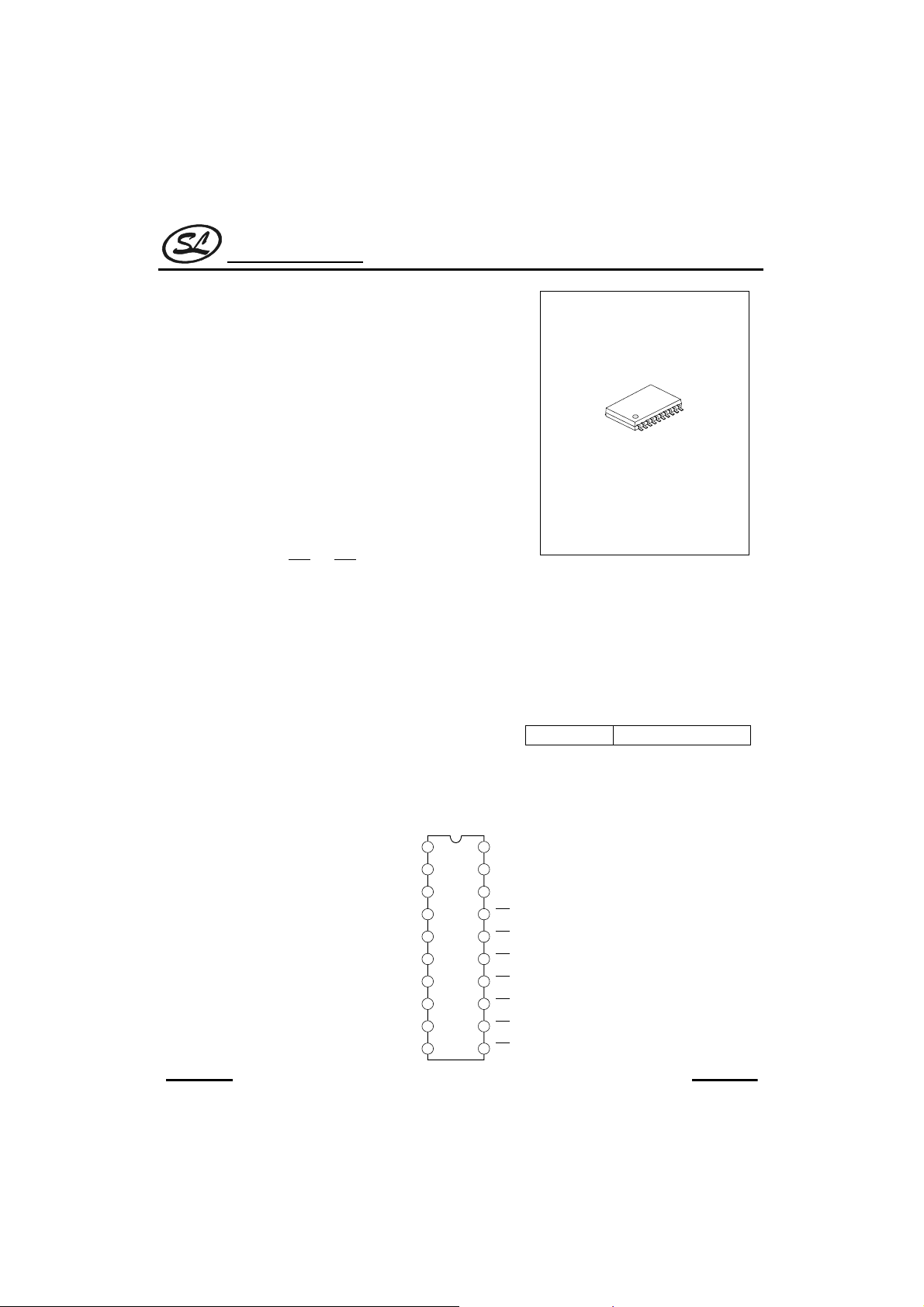
PIN CONFIGURATIONS
HANGZHOU SILAN MICROELECTRONICS JOINT-STOCK CO.,LTD
XTAL1
XTAL2
SN7
SN0
SN1
SN2
SN3
SN6
SN4
SN5
1
2
3
4
5
6
7
8
9
10
20
VDD
19
Lout
18
VSS
DR6
17
16
DR0
15
DR1
SC8521
14
DR2
13
DR3
12
DR4
11
DR5
REV: 1.3 2002.03.01
1
Page 2
Silan
Semiconductors
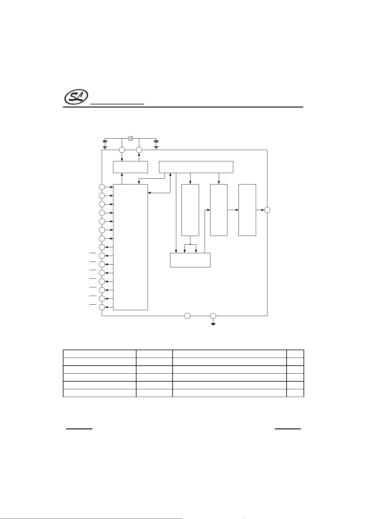
BLOCK DIAGRAM
XTAL1 XTAL2
SC8521
432kHZ
1 2
SN0
SN1
SN2
SN3
SN4
SN5
SN6
SN7
DR0
DR1
DR2
DR3
DR4
DR5
DR6
4
5
6
7
9
10
8
3
16
15
14
13
12
11
17
OSCILLATOR
KEY SCANNING
TIMING GENERATOR AND CONTROL
1K x 8 ROM
PULSE GENERATOR
SHIFT REGISTER
20 18
V
DD
V
SS
19
Lout
OUTPUT DRIVER
ABSOLUTE MAXIMUM RATING
Characteristic Symbol Value Unit
Supply Voltage V
PowerDissipation P
Thermal Derating
Storage Temperature T
Operating Temperature T
DD
D
K∂
STG
OPR
5V
25 mW
10
-65 ~ +150
-20 ~ +80
HANGZHOU SILAN MICROELECTRONICS JOINT-STOCK CO.,LTD
REV: 1.3 2002.03.01
2
mW/°C
°C
°C
Page 3
Silan
Semiconductors
SC8521
ELECTRICAL CHARACTERISTICS
(Tamb=25°C, unless otherwise specified)
Symbol Parameter Test condition Min Type Max Unit
Operating supply voltage V
Supply current I
Quiescent current IDD(q)
Operating ambient temperature T
Sense lines (input only and will have a weak internal pull-up resistance)
LOW level input voltage V
HIGH level input voltage V
Pull-up resistance Rpu VDD=3V 50 -- 100
Driver lines (output only; open drain; maximum on-resistance when LOW)
Maximum on-resistance Ron VDD=3V -- -- 2
Output drive (has a weak pull-up resistance)
Source current Isink VDD=3V; VO=1.5V 3.5 4.5 5.5 mA
DD
DD
VDD=3V; TA=25°C
V
=3V; TA=25°C
DD
A
IL
IH
2.2 -- 4.5 V
-- -- 2 mA
-- -- 1
-10 -- +50
-- -- 0.3V
0.7V
DD
-- -- V
DD
PIN DESCRIPTION
20-pin dual in-line and small outline package (SO-20)
Pin No. Symbol Description
1 XTAL1 Oscillator input
2 XTAL2 Oscillator output
3 SN7 Sense line 7 for key matrix
4 SN0 Sense line 0 for key matrix
5 SN1 Sense line 1 for key matrix
6 SN2 Sense line 2 for key matrix
7 SN3 Sense line 3 for key matrix
8 SN6 Sense line 6 for matrix
9 SN4 Sense line 4 for matrix
10 SN5 Sense line 5 for matrix
11
12
13
14
15
16
DR5
DR4
DR3
DR2
DR1
DR0
Drive line 5 for key matrix (active LOW)
Drive line 4 for key matrix (active LOW)
Drive line 3 for key matrix (active LOW)
Drive line 2 for key matrix (active LOW)
Drive line 1 for key matrix (active LOW)
Drive line 0 for key matrix (active LOW)
µA
°C
V
KΩ
KΩ
To be continued
HANGZHOU SILAN MICROELECTRONICS JOINT-STOCK CO.,LTD
REV: 1.3 2002.03.01
3
Page 4
Silan
Semiconductors
(Continued)
Pin No. Symbol Description
17
18 VSS Ground
19 Lout Output signal
20 VDD Power supply
DR6
FUNCTION DESCRIPTION
1. Key numbering for matrix is gi ven in tables 1
Table1 key numbering for 20-pin package
Driver lines
DR5
DR4
DR3
DR2
DR1
DR0
DR6
SN0 SN7 SN1 SN2 SN3 SN6 SN4 SN5
0:BANK0 1 2 3 4 5 6 7
8:BANK19 101112131415
16:BANK2 17 18 19 20 21 22 23
24:BANK3 25 26 27 28 29 30 31
32:BANK4 33 34 35 36 37 38 39
40:BANK5 41 42 43 44 45 46 47
48:BANK6 49 50 51 52 53 54 55
SN0 connected GND, send BANK7 code. BANK0----7 see the following code table.
Drive line 6 for key matrix (active LOW)
Sense lines
SC8521
When the keys have been scanned the key-number of the activated key serves as the address of the ROM to
obtain the required codeword. Consequently,key numbers 6, 7, 14, 15, 22, 23, 30, 31, 38, 39 and 40 to 55 will not
be addressed.
The ROM contains 8 banks of 64 code words. Thus for each key a maximum of 8 different code words may be
generated. With multi-system use, 8 different systems (e.g. TV, VCR, tuner, CD etc.) may be selected. Apart from
the system bits the command bits may also be different in different banks (true multi-function keys). Selection can
be performed using the keys. For each key three bank selected bits are present that determine which bank will be
selected for the next key.
For each key an ‘inhibit’ bit is also present. When this bit is at logic 1 at an address in a given bank, and when
the corresponding key is pressed (when this bank has been selected) no transmission will take place.
A single system option is available however, whereby instead of keys jumper wire and/or a switch may be used
for bank selection. Using this option it is possible to program different transmitter models in one IC and select the
required bank by means of jumper wire. Instead of a jumper wire a side-switch may also be used to change the
HANGZHOU SILAN MICROELECTRONICS JOINT-STOCK CO.,LTD
REV: 1.3 2002.03.01
4
Page 5
Silan
Semiconductors
generated code temporarily (select different bank) to obtain multi-function keys. With this option the jumper wires
SC8521
or switch must be connected between sense line SN0 and one of the drivelines
DR0toDR6
or ground. This
means that SN0 cannot be used to connect keys and the maximum number of keys will be 49 keys for a 20-pin
package.
It is not possible to use a combination of jumper wires and selection keys for bank selection in one unit. The
output of the ROM is loaded into a shift register that provides the input bits for the pulse generator. This pulse
generator drives the output pin.
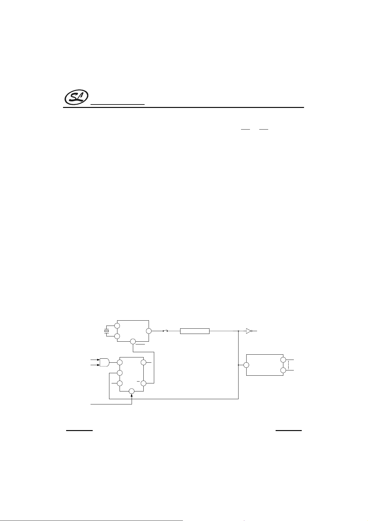
2. Timing generator
A schematic diagram of the timing generator is illustrated the oscillator frequency is 432KHz. The timing
generator is stopped when no key is activated and started again when a key is pressed.
The output of the oscillator (CLK1) is divided by 12 for 432KHz. Selection is achieved using a mask option. The
output of the divider is CLK2 which is used for clocking of the control timer. The frequency of CLK2 is 36 KHz and
the inverse is used to generate the output pulses in the subcarrier frequency. By mask option the duty factor can
be chosen to be 25% or 33%.
The control timer has a length of 4096 subcarrier (pulse) periods. This is equal to the transmission repletion time.
A bit time is equal to 64 pulses and the repetition time is 64 bit times. The control timer provides the timing of the
key scanning, the ROM access and the code transmission. When the control timer has arrived at a certain state
and no key has been pressed for at least 28 ms, a stop signal will be generated which will stop the oscillator. All
drivelines will then be set to logic 0. As soon as a key is pressed one of the sense lines will become logic 0. This
will generate a start signal, which will restart the oscillator.
no key
end control
start input
STOP
Q
CLK1
432 kHz INV
CLK2
CONTROL
DIVIDE-BY-4096
432kHz
OSCILLATOR DIVIDE BY 12
SQ
CLK
R
CLR
Timer schematic diagram
HANGZHOU SILAN MICROELECTRONICS JOINT-STOCK CO.,LTD
5
pulse
C0
TIMER
C11
REV: 1.3 2002.03.01
Page 6

Silan
Semiconductors
3. Single system
SN0 should be connected to one of the drivelines or ground.
The bank that will be selected is equal to drive line number to which SN0 is connected. When connected to
ground the number will be 7. This achieved by loading the bank select flip-flops BS0 to BS2 with the contents of
C5 to C7 of the control timer when sense line SN0 is at logic 0. In this way it is possible to use two different
systems in one transmitter by using a side switch. With this option SN0 cannot be used to connect keys, so the
maximum number of keys will be lower (49 keys with 20-pin IC).
4. Multi system
The bank is selected by key for maximum 8 different systems (e.g. TV, VCR, CD, etc.), any key is flexible for
bank selection. When a user inserts a new battery, the default bank is always in bank 7. If only bank 7 is used,
then maximum number of key can be 56 keys for a 20-pin IC
5. ROM
SC8521
Logic1 Logic0
A schematic diagram of the ROM is illustrated. The ROM is divided into 8 banks of 2 × 64 bytes. Bank selection
is performed using flip-flops BS0 to BS2 that are the 3 highest bits of the address. With the ‘single system’ these
bits are loaded from the 3 MSBs of the scan control when SN0 = 0. At power-on the bank select flip-flops will be in
an arbitrary state.
When a key was activated, the key number is stored in the 6-bit key register. This register forms the lower bits of
the ROM address. For each command the ROM will be accessed twice. This gives 16 bits in total (M0L to M7L
and M0H to M7H). The bits are described in Table 2.
Table2 ROM bit description
Bits Function
M0LtoM5L Commandbits0to5
M6L
M7L
M0H to M4H System bits 0 to 4
M5H to M7H
Field bit. This bit indicates whether command codes 0 to 63 are used (filed bit is at logic 1)
or command codes 64 to 127 are used (filed bit is at logic 0).
Inhibit bit. When this bit is at logic 1 no transmission will take place. When this bit is at
logic 0 the appropriate code word will be transmitted.
Bank select. Will be stored in BS0 to BS2 when the ‘multi-system’ option is selected. With
single system bits M5H to M7H are don’t care.
HANGZHOU SILAN MICROELECTRONICS JOINT-STOCK CO.,LTD
REV: 1.3 2002.03.01
6
Page 7

Silan
Semiconductors
6. Pulse output
The bits of the remote control word, as indicated by the addressed ROM locations, are loaded into a shift
register every bit-time this register is shifted. The output is used to generate a logic1 in the biphase (Manchester)
coding, modulated with a frequency of 36 KHz. The duty factor of the modulation pulses may be selected
(optionally) to be 25% or 33.3%. The output of the pulse generator controls the output driver that can provide a
maximum current of 5 mA.
DR5
DR4
DR3
DR2
DR1
DR0
DR6
SN0
SC8521
SN7
SN1
SN2
SN3
SN6
SN4
SN5
Scan timing.
HANGZHOU SILAN MICROELECTRONICS JOINT-STOCK CO.,LTD
REV: 1.3 2002.03.01
7
Page 8

Silan
R
Semiconductors
OM 1Kx8
BANK 0 LSB
BANK 1 LSB
address
BS2
BS1
BS0
KN5
KN4
KN3
KN2
KN1
KN0
M7H M6H M5H M4H M3H M2H M1H M0H M7L M6L M5L M4L M3L M2L M1L M0L
SYSTEM DEVELOPMENT
1. Software (SC8521)
A PC program is provided that enables the user to fill in system and command codes for each keys number in
each bank. This program converts the input data into a ROM code-file needed to produce the metal mask and to
program an EPROM to be used in the hardware emulator.
BANK 2 LSB
BANK 3 LSB
BANK 4 LSB
BANK 5 LSB
BANK 6 LSB
BANK 7 LSB
BANK 0 MSB
BANK 1 MSB
BANK 2 MSB
BANK 3 MSB
BANK 4 MSB
BANK 5 MSB
BANK 6 MSB
BANK 7 MSB
ROM schematic diagram
SC8521
2. Hardware
An emulator is available that functionally emulates the IC. An EPROM with the ROM code information is
inserted into the emulator to produce the required remote control codes corresponding to the keys in the prototype
device.
HANGZHOU SILAN MICROELECTRONICS JOINT-STOCK CO.,LTD
REV: 1.3 2002.03.01
8
Page 9

Silan
Semiconductors
INTERNAL PIN CONFIGURATION
SC8521
1. Pin configuration for pin SN0 2. Pin configuration for pins SN1 to SN7
V
DD
4
3,5to10
V
DD
V
DD
3. Pin configuration for pins DR0 to DR6 4. Pin configuration for pin Lout
V
DD
V
DD
V
DD
11 to 17
APPLICATION CIRCUIT
432 kHz
100pF
100pF
1
XTAL1
2
XTAL2
SN7
3
4
SN0
5
SN1
6
SN2
7
SN3
8
SN6
9
SN4
10
SN5
V
20
DD
1k
¡
19
LOUT
18
V
SS
DR6
17
16
DR0
15
DR1
SC8521
14
DR2
13
DR3
12
DR4
11
DR5
k7
k6
k5
k4
k3
k2
B0
k1
k15
k14
k13
k12
k11
k10
47F
¡
2
k23
k31
k39
k47
k55
k22
k30
k38
k46
k54
k21
k29
k37
k45
k53
k20
k28
k36
k44
k52
k19
k27
k35
k43
k51
k18
k26
k34
k42
k50
B1
B2
B3
B4
B5
B6
k9
k17
k25
k33
k41
k49
19
Application diagram (SO20 package)
HANGZHOU SILAN MICROELECTRONICS JOINT-STOCK CO.,LTD
REV: 1.3 2002.03.01
9
Page 10

Silan
Semiconductors
SC8521
INSTRUCTION AND SIGNAL OUTPUT FORMAT (Binary)
Key Bank0 Bank1 Bank2 Bank3
k0
k1
k2
k3
k4
k5
k6
k7
k8
k9 10000111001110 11000100000011 11001011000011 11010100000011
k10 10000111001101 11000100100001 10001011011011 11010100100001
k11 10000000100001 11000100100000 10001011011001 11010100100000
k12 11000111111010 10000100001111 11001011100000 11010101111111
k13 11000111010111 11000100001001 11001011001001 11010100001001
k14 11000000100100 11000100110101 11001011100001 11010100110101
k15 11000111010110 11000100000110 11001011000110 11010100000110
k16 / / / /
k17 10000111000100 10000100110100 11001011011010 11010000001101
k18 11000111011101 11000100001010 11001011101001 11010100001011
k19 / 10000100110001 10001011111110 10010000001111
k20 10000111000101 10000100001100 11001011010110 11010001101011
k21 11000111110110 10000100110111 11001011010111 11010001011111
k22 11000111010101 10000100000101 11001011111110 11010001101110
k23 11000111110101 10000100110110 11001011010000 11010000010000
k24 / / / /
k25 10000000111010 11000100000010 11001011000010 11010100000010
k26 10000000010001 10000100110011 10001011010001 10010100110011
k27 10000000010010 10000100110010 10001011010000 10010100110010
////
10000111010011 11000100101110 11001011100100 11010100101011
10000111010010 11000100011101 11001011010011 11010100011101
11000111101100 11000100011111 11001011010010 11010100110010
11000000001100 10000100100000 11001011001100 11010100111111
11000111010001 10000100101100 11001011100101 10010100101100
11000111011110 11000100101101 11001011001111 11010100101101
11000111010000 11000100011100 11001011001101 11010100011100
////
(To be continued)
HANGZHOU SILAN MICROELECTRONICS JOINT-STOCK CO.,LTD
REV: 1.3 2002.03.01
10
Page 11

Silan
Semiconductors
Continued
Key Bank0 Bank1 Bank2 Bank3
k28 11000000001101 10000100011000 11001011100010 11010010111111
k29 11000111011001 11000100001000 11001011001000 11010100001000
k30 10000000010000 11000100110000 11001011100011 11010100110000
k31 11000111011000 11000100000101 11001011000101 11010100000101
k32 / / / /
k33 11000111011101 11000100000001 11001011000001 11000100000001
k34 11000111011100 11000100111011 10001011011010 11010100111011
k35 10000000010101 11000100101010 10001011011000 11010100110100
k36 11000000100011 11000100101000 10001011111111 11010001111111
k37 11000111011011 11000100000111 11001011000111 11010100000111
k38 10000111111111 11000100110110 11001011101101 11010100110110
k39 11000111011010 11000100000100 11001011000100 11010100000100
k40 / / / /
k41 11000111000000 11000100010001 / 10010000000000
k42 / 11000100010000 / 10010000000110
k43 11000111011100 11000100100100 10001011011101 11010100100100
k44 11000111010100 11000100000000 11001011000000 11010100000000
k45 / 10000100110000 / 11010000001111
k46 11000111100111 10000100000110 10001011011100 11010100001111
k47 / 11000100001100 /
k48 / / / /
k49 10000111000011 11000100101011 11001011011011 11010000100110
k50 11000111010011 11000100001111 11001011101110 11010001001100
k51 11000111010010 10000100101011 11001011101011 10010100101011
k52 10000111000110 10000100001011 11001011011000 11010001100001
k53 11000111110111 10000100000011 11001011011001 11010001011110
k54 11000111011111 10000100000100 11001011111111 1101000110000
k55 11000111110100 10000100101111 11001011010001 11010000010001
SC8521
HANGZHOU SILAN MICROELECTRONICS JOINT-STOCK CO.,LTD
REV: 1.3 2002.03.01
11
Page 12

Silan
Semiconductors
Key Bank4 Bank5 Bank6 Bank7
k0////
k1 11010100011101 10000000101101 10000000101101 11000000110010
k2 11010001011111 10000000101100 10000000101100 11000000110110
k3 11010001011110 10000000101011 10000000101011 11000000110111
k4 11010100001100 11000000001100 11000000001100 11000000001100
k5 11010100011100 10000000101111 10000000101111 11000000110101
k6 10010100101011 10000000111110 10000000111110 10000000111110
k7 11010100101011 10000000101110 10000000101110 11000000110100
k8////
k9 11010100000011 11000000000011 11000000000011 11000000000011
k10 11010100100001 11000000100110 10000000100001 11000000100110
k11 11010100100000 10000000010110 10000000010110 11000000010000
k12 11010100101101 11000000001110 11000000001110 11000000001110
k13 11010100001001 11000000001001 11000000001001 11000000001001
k14 11010100110101 11000000100100 11000000100100 11000000100100
k15 11010100000110 11000000000110 11000000000110 11000000000110
k16 / / / /
k17 11010000011010 11000000101100 11000000101100 11000000101100
k18 11010001111111 11000000010000 10000000011001 10000000011001
k19 11010100111011 / 10000000100101 /
k20 11010000010110 11000000101011 11000000101011 11000000101011
k21 11010000010111 11000000101010 11000000101010 11000000101010
k22 11010010111111 11000000100001 10000000100111 11000000001011
k23 11010000010000 11000000101011 11000000101011 11000000101101
k24 / / / /
k25 11010100000010 11000000000010 11000000000010 11000000000010
k26 11010100110010 10000000010001 10000000010001 11000000100001
k27 11010100110100 10000000010010 10000000010010 11000000111011
k28 11010100001011 11000000001101 11000000001101 11000000001101
SC8521
(To be continued)
HANGZHOU SILAN MICROELECTRONICS JOINT-STOCK CO.,LTD
REV: 1.3 2002.03.01
12
Page 13

Silan
Semiconductors
(Continued)
Key Bank4 Bank5 Bank6 Bank7
k29 11010100001000 11000000001000 11000000001000 11000000001000
k30 11010100110110 10000000010000 10000000010000 11000000100000
k31 11010100000101 11000000000101 11000000000101 11000000000101
k32 / / / /
k33 11000100000001 11000000000001 11000000000001 11000000000001
k34 11010001100001 10000000110101 10000000110101 10000000110101
k35 11010001100000 10000000010101 10000000010101 11000000010001
k36 11010000100110 11000000100011 11000000100011 11000000100011
k37 11010100000111 11000000000111 11000000000111 11000000000111
k38 10010100101100 11000000001111 11000000001111 11000000001111
k39 11010100000100 11000000000100 11000000000100 11000000000100
k40 / / / /
k41 / 11000111000000 10000000011010 11000111000000
k42 / / 10000000011111 /
k43 10010100110011 11000000111000 11000000111000 11000000111000
k44 11010100000000 11000000000000 11000000000000 11000000000000
k45 11010100110000 10000000110001 10000000110001 /
k46 10010100110010 11000000100010 11000000100010 11000000100010
k47
k48 / / / /
k49 11010000011011 11000000111100 11000000111100 11000000111100
11000111111010 11000111111010 11000111111010
SC8521
k50 11010100111111 11000000010001 10000000011000 10000000011000
k51 11010100100100 11000000111111 11000000111111 11000000111111
k52 11010000011000 11000000101001 11000000101001 11000000101001
k53 11010000011001 10000000111010 10000000111010 11000000011110
k54 11010101111111 11000000100000 10000000100110 11000000001010
k55 11010000010001 11000000101110 11000000101110 11000000101110
1The number after K is the key code number.
The number after B is BANK0, BANK1 number. When SN0 connect the GND, it sends BANK7.
2
Don’t compatible with PCA8521pins.
3
HANGZHOU SILAN MICROELECTRONICS JOINT-STOCK CO.,LTD
REV: 1.3 2002.03.01
13
Page 14

Silan
Semiconductors
PCB WIRE LAYOUT SCHEMATIC:
SC8521
Transmitting tube output ground line
The transmitting tube ground line and IC ground line should
layout separated or overstriking ground line.
The above IC only use to hint, not to specified.
Note:
* In wire layout, the power filter capacitor should near to IC.
* In wire layout, should avoid power line and ground line too long.
* Recommended infrared transmit unit and IC ground line should layout separated, or overstriking lines.
* The emitter of triode connect 1
* Recommended triode use 9014.
resistor at least.
HANGZHOU SILAN MICROELECTRONICS JOINT-STOCK CO.,LTD
14
REV: 1.3 2002.03.01
Page 15

Silan
Semiconductors
PACKAGE OUTLINE
SOP-20-375-1.27 Unit: mm
0.4
0.3
B
B
7.6
10.2
1.27
12.7B0.25
11.43
0.4
B
0.1
3.1MAX
SC8521
9.525(375)
0.25B0.05
HANGZHOU SILAN MICROELECTRONICS JOINT-STOCK CO.,LTD
REV: 1.3 2002.03.01
15
Page 16

Silan
Semiconductors
Attach
SC8521
Revision History
Data REV Description Page
2001.09.18 1.0 Original
2001.01.03 1.1 Modify the order of the pin in key matrix table 4
Modify the diode direction in “APPLICATION CIRCUIT”
2002.01.19 1.2
2002.03.01 1.3
Add the Binary “instruction and signal output format table”
Add the note of instruction table.
The 102pF capacitor change to 100pF in “APPLICATION CIRCUIT”
Add the “PCB wire layout schematic”
Modify the “Package outline”
9
10~13
13~14
9
14
15
HANGZHOU SILAN MICROELECTRONICS JOINT-STOCK CO.,LTD
REV: 1.3 2002.03.01
16
 Loading...