

Page 1
Silan
Semiconductors
REMOTE CONTROL DECODER
DESCRIPTION
The SC5272 is a remote control decoder paired with SC5262
utilizing CMOS technology. It has a maximum of 12-bits of tri-state
address pins providing up to 531,441(or 3
thereby, drastically reducing any code collision and unauthorized
code scanning possibilities.
FEATURES
* Low power consumption and very high noise immunity
* Up to 12 tri-state code address pins or 6 data pins
* Wide operating voltage range(Vcc=3V ~ 15V)
* Single resistor oscillator
* Latch or Momentary output type
APPLICATION
* Home/automation security system
* Remote control toys or for industrial use
* Remote control fan
* Garage door controller
ORDERING INFORMATION
12
) address codes;
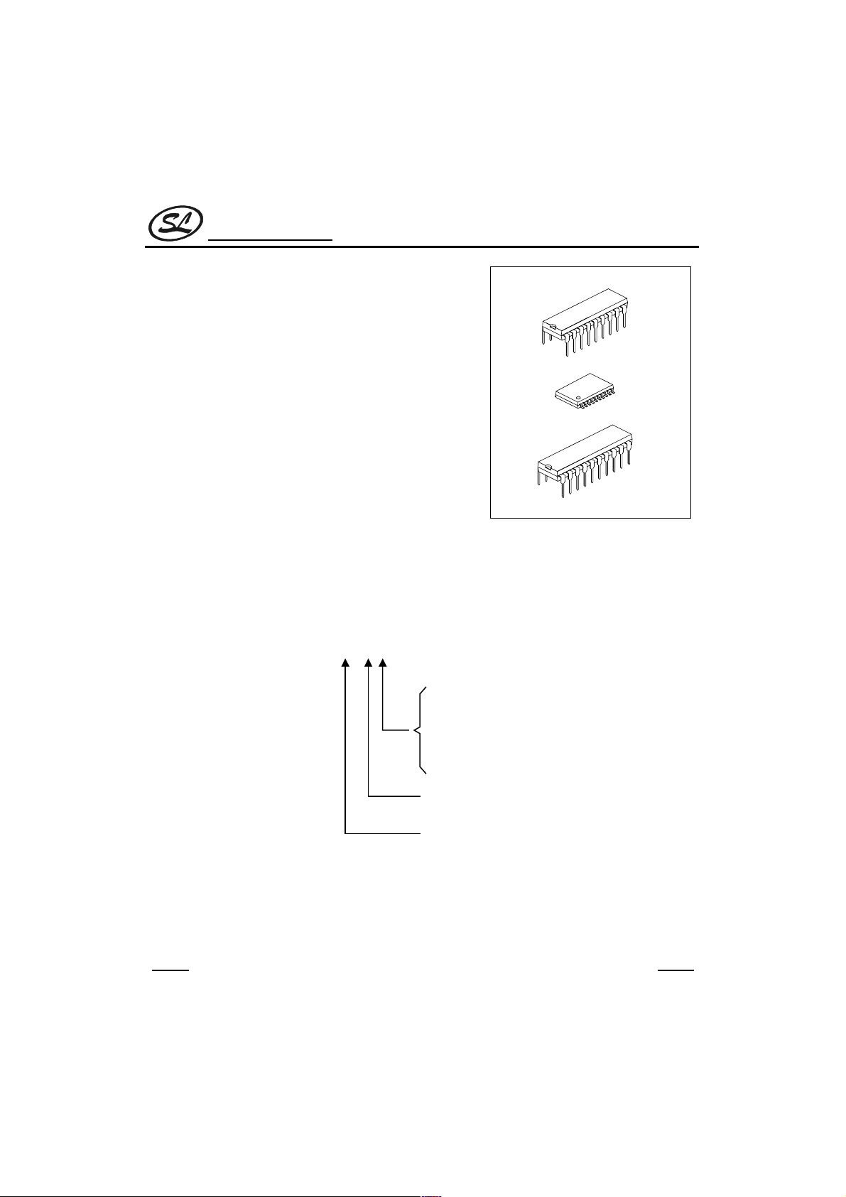
SC5272
DIP-18
SOP-20
DIP-20
SC5272X-XX
Data Bits:
0: 0 data bit(can be omitted)
2: 2 data bits
3: 3 data bits
4: 4 data bits
5: 5 data bits
6: 6 data bits
L: Latch Type
M: Momentary Type
S: SOP-20 Package
D: DIP-20 Package
Omitted: DIP-18 Package
HANGZHOU SILAN MICROELECTRONICS JOINT-STOCK CO.,LTD
1
Rev: 1.0 2000.12.31
Page 2
Silan
Semiconductors
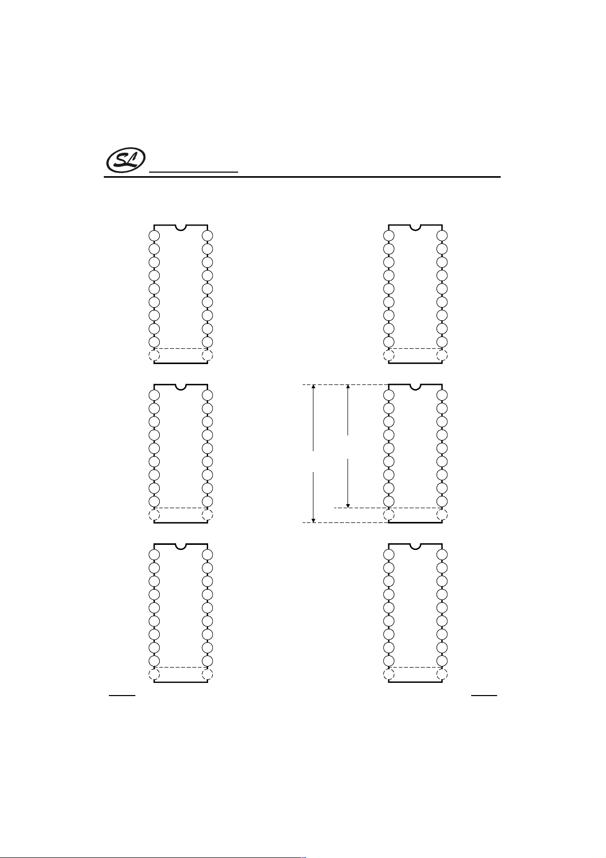
PIN CONFIGURATION
SC5272
A0
A1
A2
A3
A4
A5
A6
A7
Vss
NC
A0
A1
A2
A3
A4
A5
A6
A7
Vss
NC
18 Pin
A0
A1
A2
A3
A4
A5
A6
A7
Vss
NC
A0
A1
A2
A3
A4
A5
A6
A7
Vss
NC
1
SC5272-M2/L2SC5272-M4/L4SC5272-M6/L6
1
1
SC5272SC5272-M3/L3SC5272-M5/L5
1
Vcc
VT
OSC1
OSC2
Din
A11
A10
A9
A8
NC
Vcc
VT
OSC1
OSC2
Din
D0
D1
D2
A8
NC
20 Pin
Package
Package
Vcc
VT
OSC1
OSC2
Din
D0
D1
A9
A8
NC
Vcc
VT
OSC1
OSC2
Din
D0
D1
D2
D3
NC
A0
A1
A2
A3
A4
A5
A6
D4
Vss
NC
1
Vcc
VT
OSC1
OSC2
Din
D0
D1
D2
D3
NC
A0
A1
A2
A3
A4
A5
D5
D4
Vss
NC
1
Vcc
VT
OSC1
OSC2
Din
D0
D1
D2
D3
NC
HANGZHOU SILAN MICROELECTRONICS JOINT-STOCK CO.,LTD
Rev: 1.0 2000.12.31
2
Page 3
Silan
Semiconductors
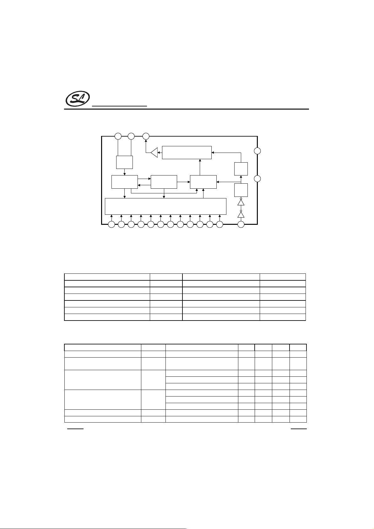
BLOCK DIAGRAM
OSC1OSC2
VT
171615
SC5272
Data
14
Din
18
Vcc
9
Vss
Output Logic
OSC
System
Timing
Tri-stateAddress Data Detect
A0 A1 A2 A3 A4 A5
The Pin configurations are for DIP-18 package and are also some different with the SC5272 suffix
Control
Logic
A6 A7 A8 A9 A10 A11
(please refer to the Pin Configuration)
Compare
Logic
87654321 11 12 13
10
Sync.
Detect
Detect
ABSOLUTE MAXIMUM RATINGS
Characteristic Symbol Value Unit
Supply Voltage Vcc -0.3 ~ 16.0 V
Input Voltage Vi -0.3 ~ Vcc+0.3 V
Output Voltage Vo -0.3 ~ Vcc+0.3 V
Maximum Power Dissipation(Vcc=12V) Pa 300 mW
Operating Temperature Topr -20 ~ +70
Storage Temperature Tstg -40 ~ +125
(Ta=25°C)
°C
°C
ELECTRICAL CHARACTERISTICS
(Ta=25°C,Vcc=12V,unless otherwise specified)
Characteristic Symbol Test Condition Min Typ. Max Unit
Supply Voltage Vcc 3 15 V
Supply Current Icc Vcc=12V,OSC stops
Dout Output driving Current I
Dout Output sinking Current I
Input HighVoltage V
Input Low Voltage V
OH
OL
IH
IL
A0~ A11 Open
Vcc=5V,VOH=3V -3 mA
Vcc=8V,VOH=4V -6 mA
Vcc=12V,VOH=6V -10 mA
Vcc=5V,VOL=3V 2 mA
Vcc=8V,VOL=4V 5 mA
Vcc=12V,VOL=6V 9 mA
0.7Vcc Vcc V
0.02 0.3
00.3VccV
HANGZHOU SILAN MICROELECTRONICS JOINT-STOCK CO.,LTD
Rev: 1.0 2000.12.31
3
µA
Page 4
Silan
Semiconductors
PIN DESCRIPTION
Pin No.
18 PIN 20 PIN
1~6 1~6 A0~A5 I
7~8
10~13
14 16 DIN I
15 17 OSC1 I Oscillator pin 1
16 18 OSC2 O Oscillator pin 2
17 19 VT O
18 20 Vcc -- Positive Power Supply
9 9 Vss -- Negative Power Supply
-- 10~11 NC -- No Connection
7~8
12~15
Pin Name I/O Description
Code Address pins No. 0~5. These six tri-state pins are
detected by SC5272 to determine the encoded waveform bit
0 ~bit 5. Each pin can be set to “0”,”1”,”f”(floating).
Code Address pins No.6~11/data pins No.5~0. These six
pins are used higher address input bits or data output pins
depending on the versions of SC5272 used.When these
pins are used as address pins, they are tri-state input pins
A6/D5~A11/D0 I/O
and can be set to “0”,”1”,”f”.When they are used as output
pins, they are driven to Vcc if (1) the address decoded from
the waveform that was received matches the address setting
at address input pins, and (2) the corresponding data bits
received is a “1” bits. Otherwise, they are driven to Vss.
Data Input Pin. The encode waveform received is serially fed
to SC5272 at this pin.
A resistor connected between
these two pins determine the
fundamental frequency of SC5272.
Valid Transmission. Active high signal. VT in high state
signifies that SC5272 receives valid transmission waveform.
FUNCTIONAL DESCRIPTION
The SC5272 decodes the waveform received and fed into the Din pin. The waveform is decoded into code word
that contains the address, data and Sync bits. The decoded address bits are compared with the address set at the
address input pins. If both addresses match for 2 consecutive code words, SC5272 drives:
a). The data output pins whose corresponding data bits is then decoded to be a "1" bit
b). The VT output --to high voltage (high state).
SC5272
1. RF OPERATION
Code Bits
A code bit is the basic component of the encoded waveform, and can be classified as either an AD(Address/Data)
Bit or a SYNC(Synchronous) Bit.
An AD bit can be designated as bit “ 0 ”, “ 1 ” or “ f ” if it is in low, high or floating state respectively. One bit
waveform consists of two pulse cycles. Each pulse cycle has 16 oscillating time periods. For further details, please
refer to the diagram below:
a
32a
OSC
bit "0"
4a
bit "1"
bit "f"
Where: a = oscillating clock period . Bit “ f ” is only available for address bits.
12a
12a
4a
HANGZHOU SILAN MICROELECTRONICS JOINT-STOCK CO.,LTD
Rev: 1.0 2000.12.31
4
Page 5
Silan
Semiconductors
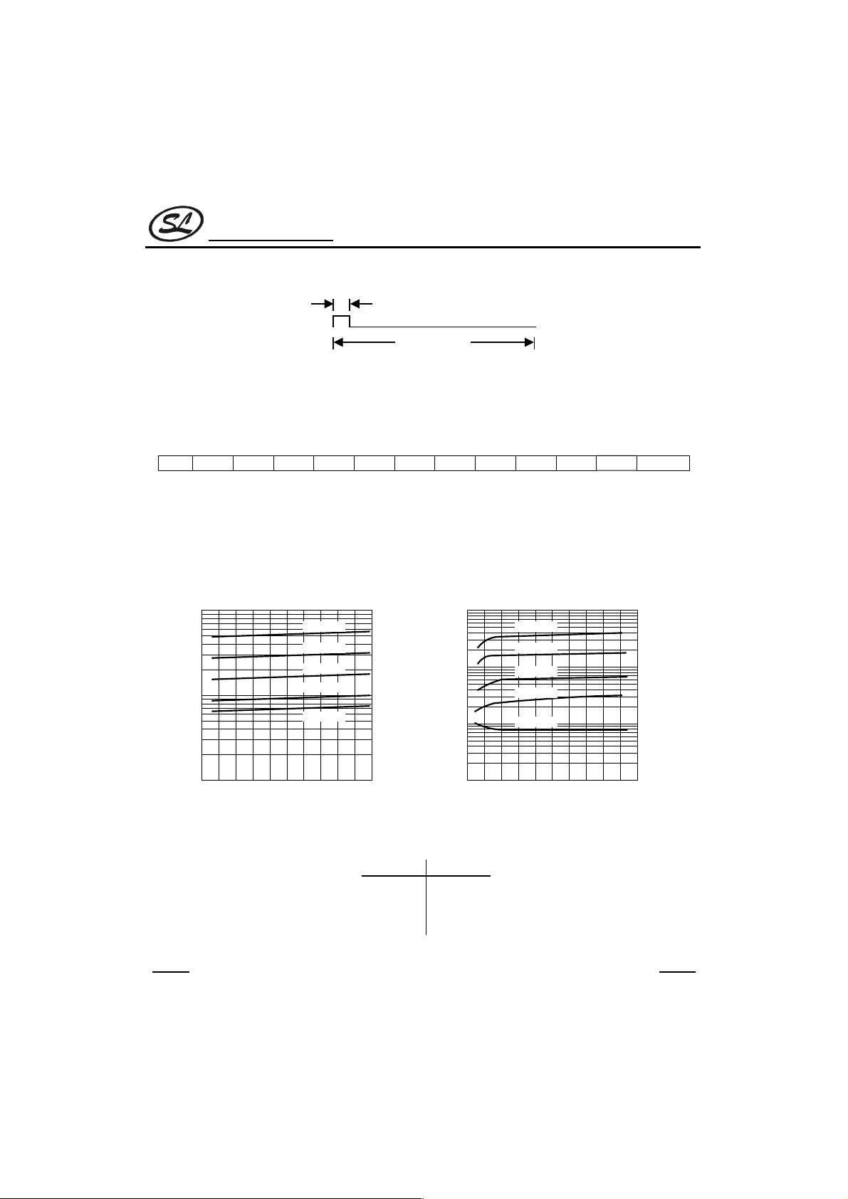
The Synchronous bit waveform is 4 bits long with 1/8 bit width pulse. Please refer to the diagram below:
1/8 bit width=4a
4 bit width=128a
Note: 1bit =32a
Code word
A group of Code Bits is called a Code Word. A Code Word consists of 12 AD bits followed by one Sync. Bit. The
12 AD bits are interpreted as either address or data bits depending on the SC5272 version used. Please refer to
the diagram below:
A0 A1 A2 A3 A4 A5 A6 A7 A8 A9 A10 A11 SYNC
Single Resistor Oscillator
The Build-in oscillator circuitry of SC5272 allows a precision oscillator to be constructed by connecting an
external resistor between OSC1 and OSC2 pins. For SC5272 to decode correctly the received waveform, the
oscillator frequency of SC5272 must be 2.5 ~8 times that of transmitting SC5262. It is a good practice to center the
SC5272 oscillator frequency in the window to gain best window margin at both sides. The typical oscillator
frequency with various resistor values for both SC5262 and SC5272 are shown below:
SC5272
Encoder OSC Frequency
100
10
Frequency (kHz)
1
0 3 6 9 12 15
Supply Voltage (V)
R=510kΩ
R=3.3MΩ
R=4.7MΩ
R=1MΩ
R=2MΩ
Decoder OSC Frequency
1000
100
10
Frequency (kHz)
1
0 3 6 9 12 15
R=100kΩ
R=240kΩ
R=510kΩ
R=1MΩ
R=2MΩ
Supply Voltage (V)
Suggested Oscillator resistor values are shown below:
SC5262 SC5272
4.7MΩ 820kΩ
3.3MΩ
1.2MΩ
HANGZHOU SILAN MICROELECTRONICS JOINT-STOCK CO.,LTD
680kΩ
200kΩ
Rev: 1.0 2000.12.31
5
Page 6
Silan
Semiconductors
2. IR OPERATION
In the IR Type of operation, the functions are similar to the above descriptions except that the output waveform
carried by SC5262-IR has a frequency of 38kHz. Details are as follows.
Code Bits
The Code Bits are further modulated with a 38kHz carrier frequency and can be”0”,”1” or “ f ” bit. Their waveform
are shown below:
OSC
"0"
"1"
"f"
Sync
20λ
60λ
160λ
620λ
SC5272
Note:λ=2 clock lengths
Code Word
A Code Word is made up of code bits and the format is the same as that of the RF Code Word.
Code Frame
Likewise, a Code Frame is made up of Code Words and the format is the same as that of RF type of operation.
Oscillator
The SC5262-IR is specially designed for infrared remote control applications and its output waveform carries
38kHz frequency. To get the 38kHz carrier frequency at the data output, the oscillator frequency must be 76kHz.
A 440kΩ resistor connected between OSC1 and OSC2 pins of SC5262-IR is recommended. Moreover, for a
matching decoder frequency, 1MΩ resistor connected between the OSC1 and OSC2 pins of SC5272 is also
recommended.
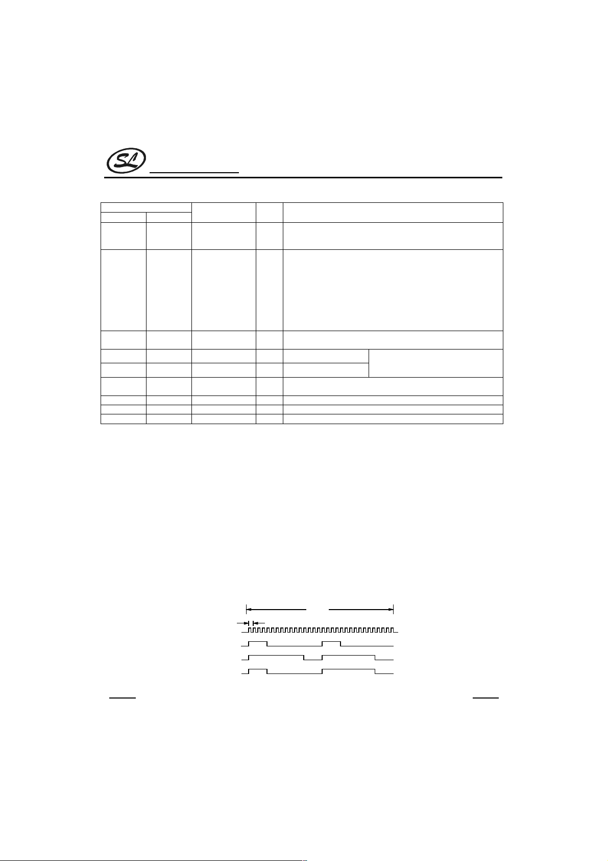
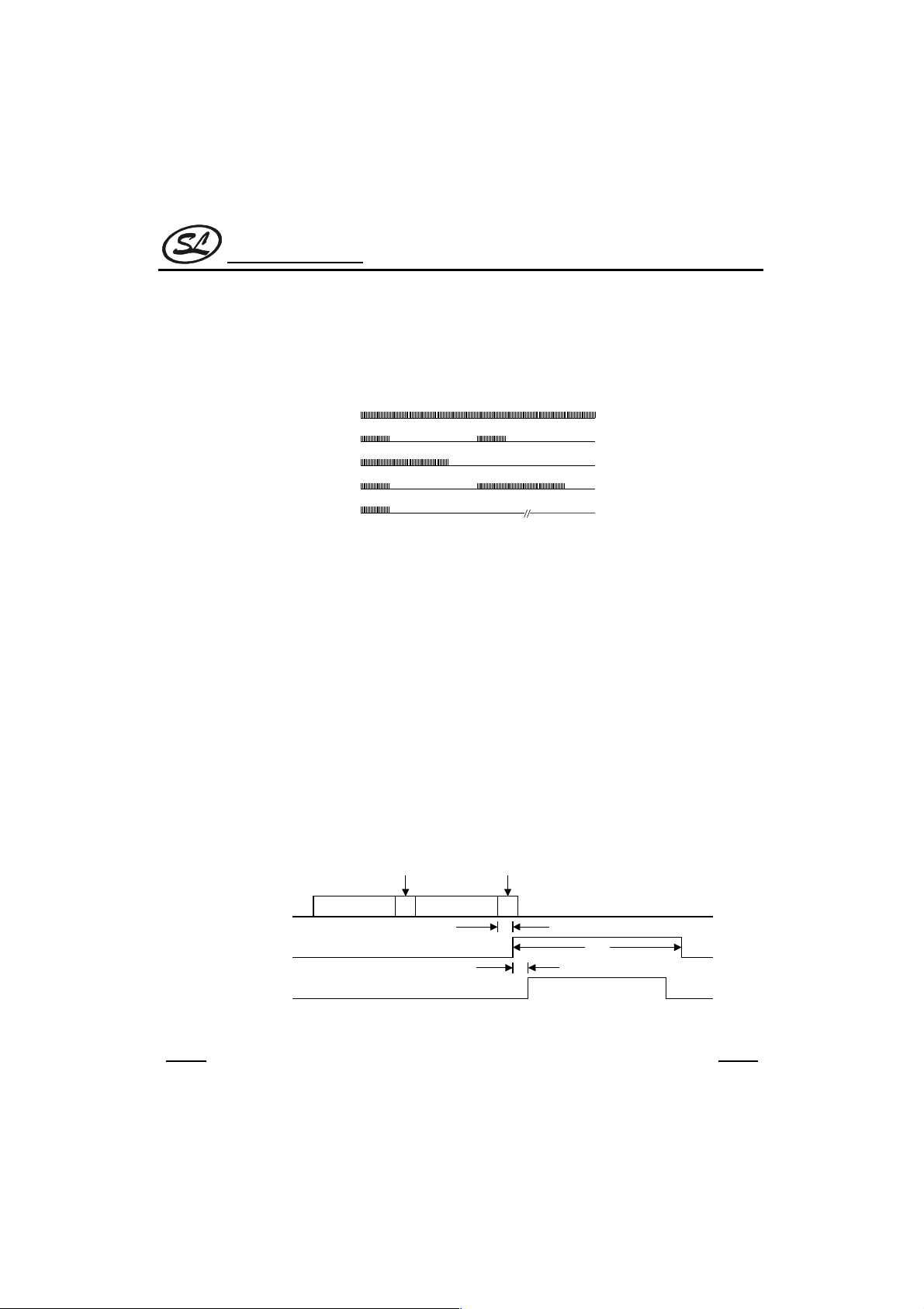
3.VALID TRANSMISSION
When the SC5272 receives a transmission code word, it initially checks whether this is a valid transmission. For
a transmission to be valid, (1) it must be a complete code word, and (2) the address bits must match the address
setting at the address pins. After two consecutive valid transmission, SC5272 (1) drives the data pins according to
the data bits received, and (2) rise VT to high voltage(high state).
The timings are shown in the following diagram.
Sync bit Sync bit
1st word 2nd word
Din
Data pins
(momentary)
VT
Ta= 8 OSC clock width
Tb= 1 OSC clock width
Tc=2 code word width
Ta
Tb
Tc
HANGZHOU SILAN MICROELECTRONICS JOINT-STOCK CO.,LTD
Rev: 1.0 2000.12.31
6
Page 7
Silan
Semiconductors
4.LATCH OR MOMENTARY DATA OUTPUT TYPE
The SC5272 uses either the latch or momentary data output type depending on the SC5272 version used. The
latch type SC5272-LXactivates the data out during transmission and this data is sustained in the memory until
another data is inputted or entered. A momentary type(SC5272-MXon the other hand, activates the data out only
during transmission. In the momentary type, the data does not remain in the memory after the transmission is
completed. Please refer to the diagram below:
SC5272
Din
Data Pins
(Momentary)
Data Pins
(Latch)
VT
Data Words Data Words
T T
Data Output X Data Output Y
Data Output X Data Output Y
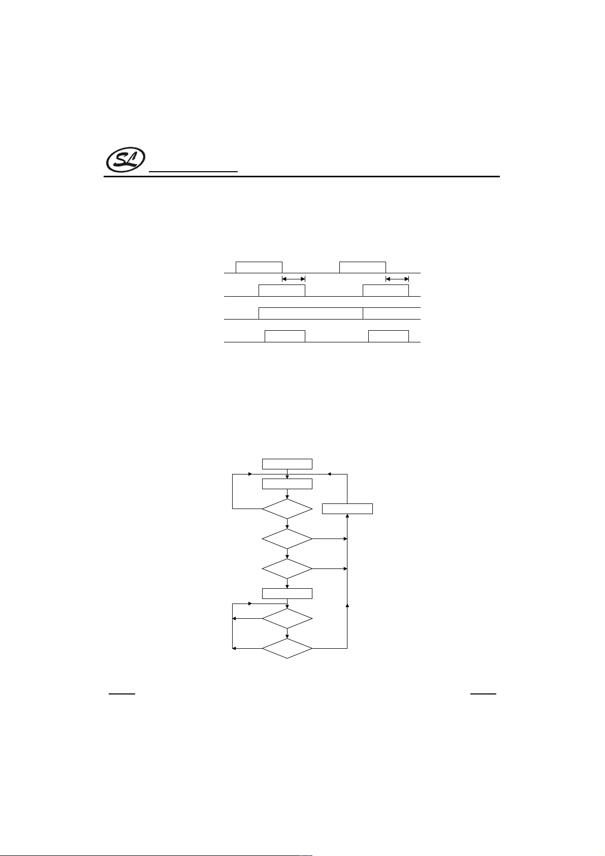
OPERATION FLOW CHART
Decoder Without Data Output Pin
1. When the power is turned on, the SC5272 activates the Stand-By Mode.
2. It then search for signals, If there is no signal received, it remains in the Stand-By Mode; otherwise, the address
bits received are compared with the address configuration of the pins.
3. The VT goes high signifying the validation of transmission only when there are two continuous frames that
contain matched address bit; otherwise, VT will not be activated and the Stand-By Mode remains active.
4. Then , the address bits are again checked. Two continuous mismatches of the address bits would disable the VT
and make the Stand-By Mode active; otherwise, the address bits are continuous checked.
Power ON
Stand-ByMode
No
Singal IN ?
Yes
Address bits
match?
Yes
Address bits
match?
Yes
Activate VT
Disable VT
No
No
Address bits
Yes
still match?
No
Address bits
Yes No
still match?
Decoder Without Data Output Pin
HANGZHOU SILAN MICROELECTRONICS JOINT-STOCK CO.,LTD
7
Rev: 1.0 2000.12.31
Page 8
Silan
Semiconductors
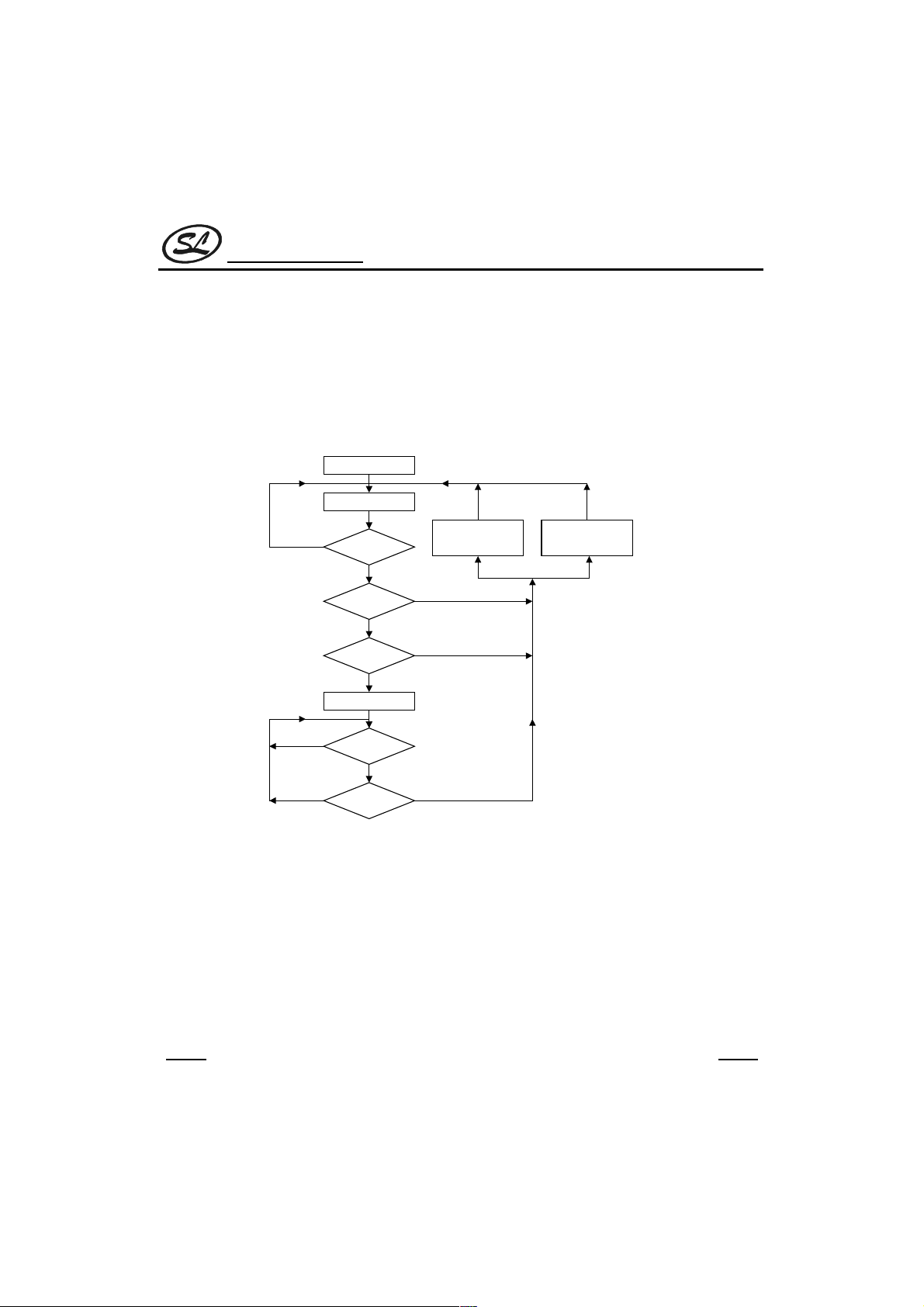
Decoder With Data Output Pins
1. When the power is turned on ,the SC5272 activates the Stand-By Mode.
2. It then searches for signal. If there is no signal received , it remains in the Stand-By Mode; otherwise, the
address bits are compared with the address configuration of the pins.
3. Whenever the address bits in frame match with that of the address configuration of the pin, the data bits are
stored into memory. Also, when this IC finds two continuous and identical data having the same address bits, the
data outputs is activated and the VT is enabled. The VT is disabled when there are two continuous mismatched
addresses. For the momentary type, the data output is reset; while for the latch type, the data output is sustained.
Power ON
Stand-By Mode
No
Singal IN ?
Yes
Address bits
match?
Yes
Address bits
match?
Yes
Activate VT
Disable VT &
Reset output Data
( for Momentary Type)
No
No
Disable VT &
Sustain output data
(For Latch Type)
SC5272
Address bits
Yes
still match?
No
Address bits
Yes No
still match?
Decoder With Data Output Pins
HANGZHOU SILAN MICROELECTRONICS JOINT-STOCK CO.,LTD
Rev: 1.0 2000.12.31
8
Page 9
Silan
Semiconductors
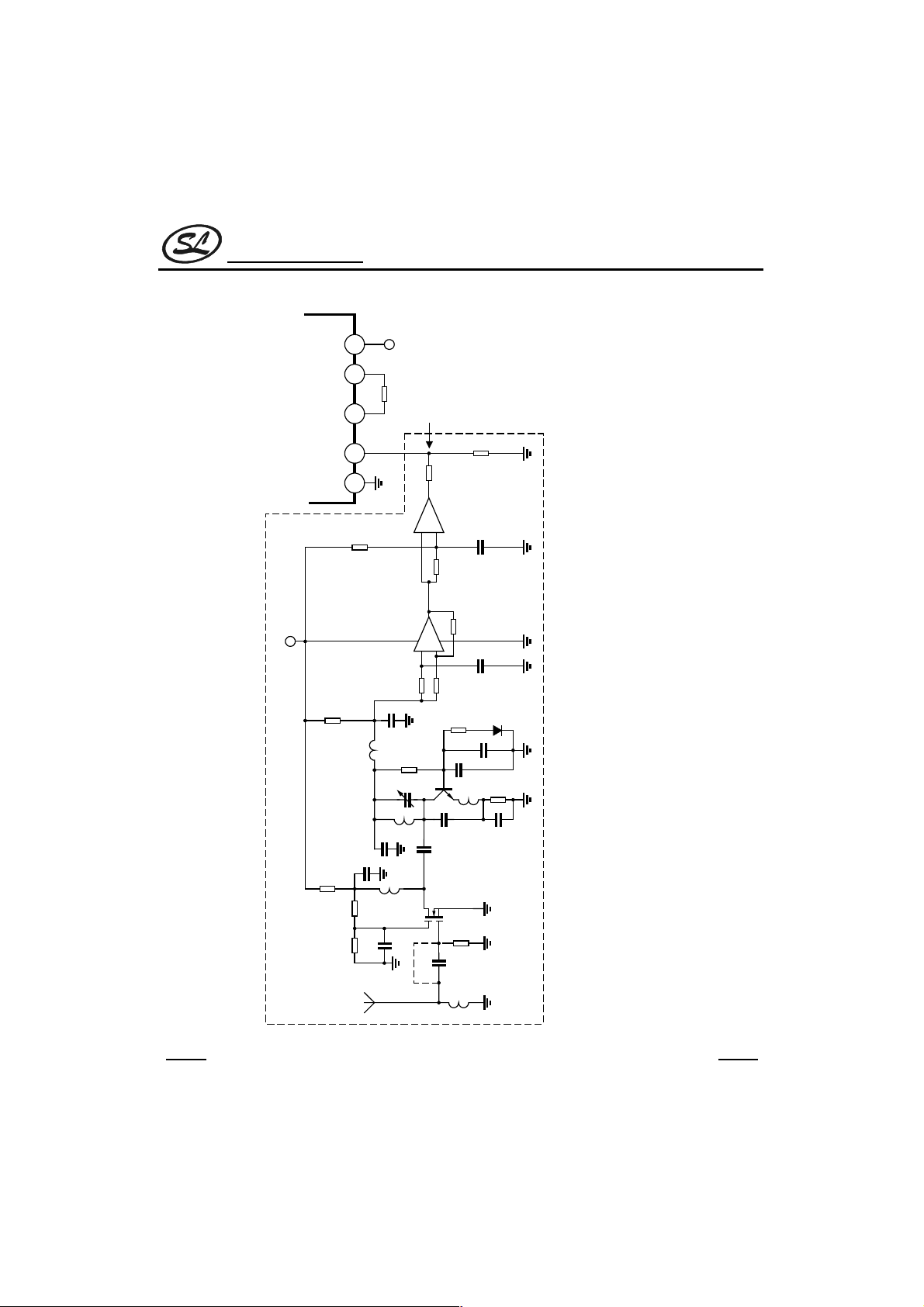
TYPICAL APPLICATION CIRCUIT
SC5272
Receiving Block
+8V
SC5272
15kΩ
1615149 18
Vcc=+8V
Rosc
A
47kΩ
27kΩ
-
+
10MΩ
100kΩ
-
+
UTC358 UTC358
47kΩ
47kΩ
0.001µF
13mH
47kΩ
7pF
1µF/16V
10MΩ
1µF/16V
1N4148
47kΩ
0.001µF
3.3µF
2.2kΩ
SC5272(No Data) RF Application Circuit
2pF
1pF
0.001µF0.001µF
100Ω
47kΩ 47kΩ
0.01µF
33pF
HANGZHOU SILAN MICROELECTRONICS JOINT-STOCK CO.,LTD
9
270pF
1.5kΩ
L1
Rev: 1.0 2000.12.31
Page 10
Silan
Semiconductors
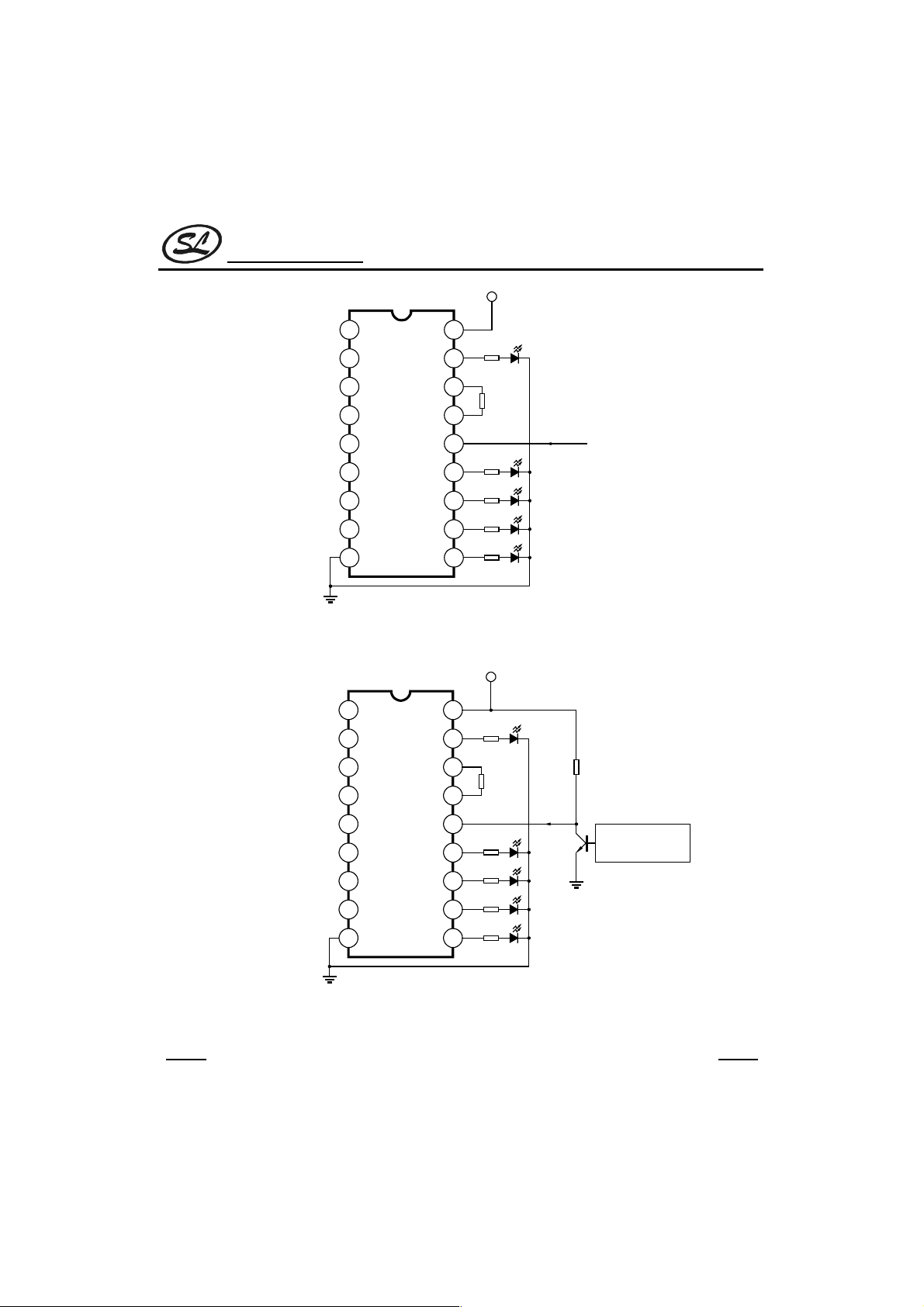
Vcc=+5V
1
18
SC5272
SC5272-L4
17
16
15
14
13
12
11
10
560Ω x5
Rosc
LED x 5
From "A" point of the
receiving Block
2
3
4
5
6
7
8
9
SC5272-L4(4 Data) RF Application Circuit
Vcc=+5V
1
2
3
4
18
17
16
15
1MΩ
10kΩ
SC5272-L4
14
13
12
11
10
560Ω x5
IR Receiver
2SC1815
LED x 5
5
6
7
8
9
SC5272-L4(4 Data) IR Application Circuit
HANGZHOU SILAN MICROELECTRONICS JOINT-STOCK CO.,LTD
Rev: 1.0 2000.12.31
10
Page 11
Silan
Semiconductors
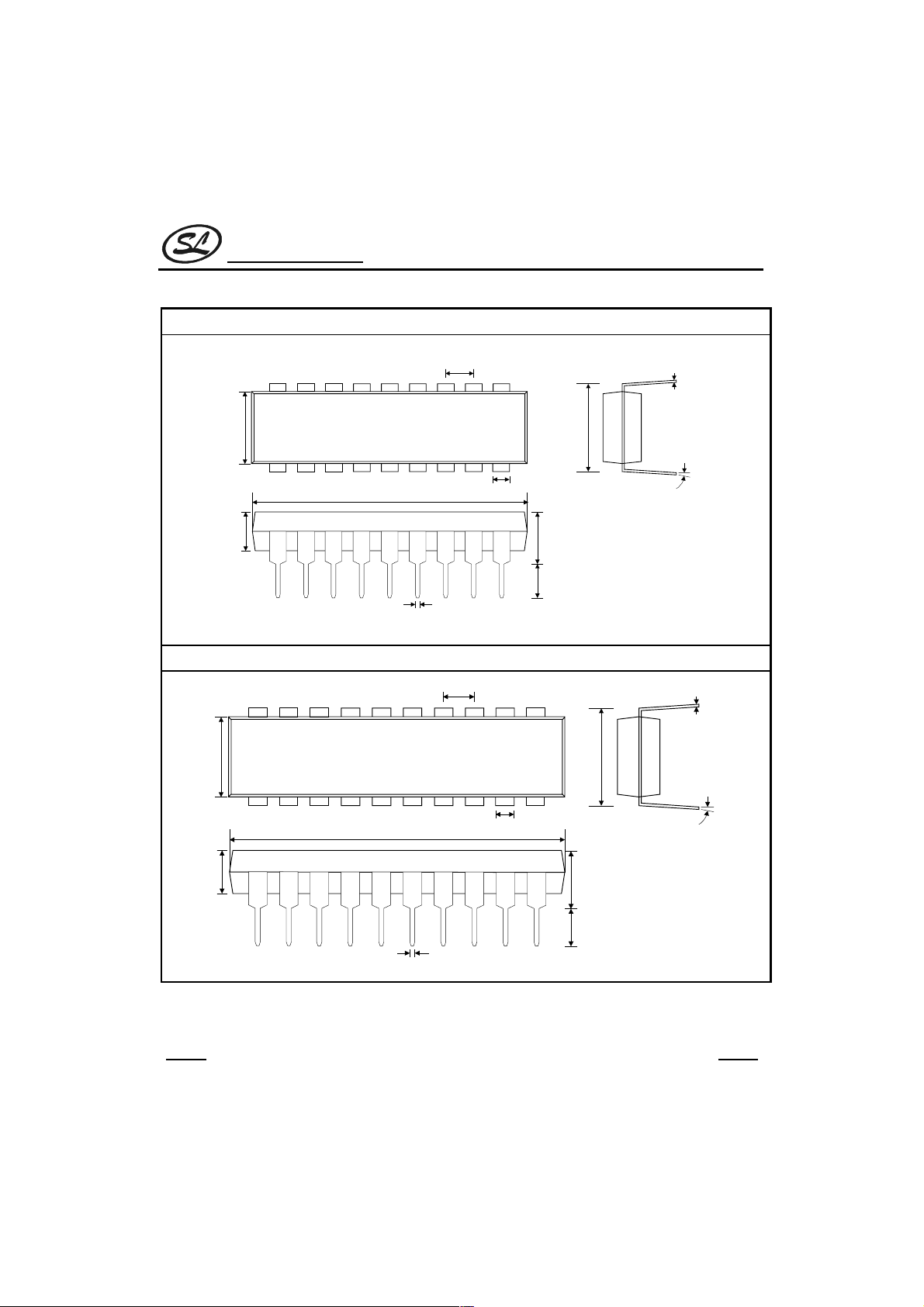
PACKAGE OUTLINE
DIP-18-300-2.54 UNIT:mm
2.54
SC5272
0.25
6.40
22.95
3.51
0.46
1.50
7.62
15 degree
5.083.30
DIP-20-300-2.54 UNIT:mm
2.54
0.25
6.40
1.50
22.95
3.51
7.62
15 degree
5.083.30
0.46
HANGZHOU SILAN MICROELECTRONICS JOINT-STOCK CO.,LTD
Rev: 1.0 2000.12.31
11
Page 12
Silan
Semiconductors
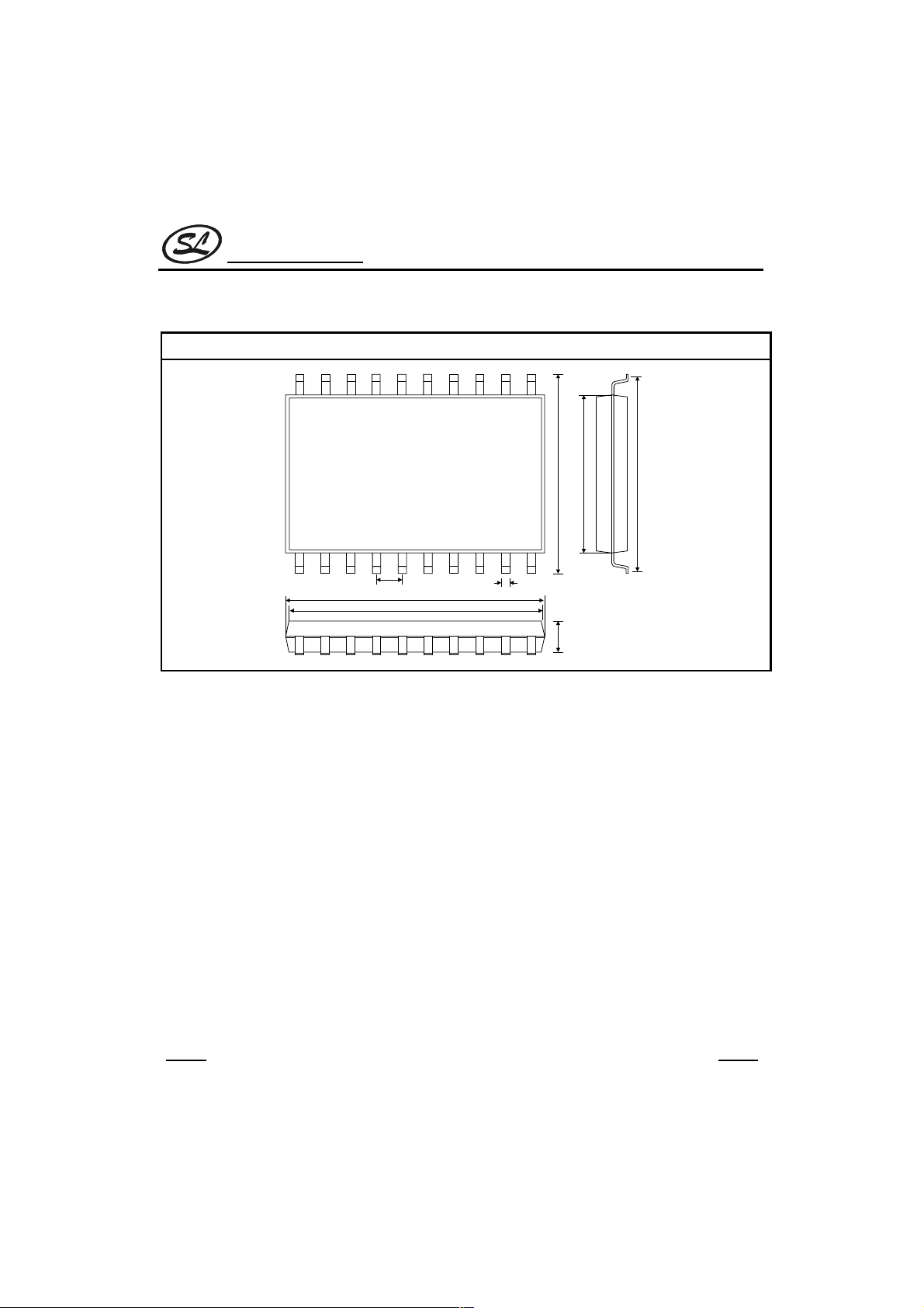
SOP-20-225-1.27 UNIT:mm
7.70
10.45
SC5272
9.53
1.27
18.02
17.62
0.41
1.95
HANGZHOU SILAN MICROELECTRONICS JOINT-STOCK CO.,LTD
Rev: 1.0 2000.12.31
12
 Loading...