

Page 1
Silan
Semiconductors
REMOTE CONTROL ENCODER
DESCRIPTION
The SC5260 is a remote control encoder paired with either
SC5260 or SC5272 utilizing COMS Technology. It encodes data and
address pins into a serial coded waveform suitable for RF
modulation. SC5260 has a maximum of 10 bits tri-state address
pins providing up to 59,049 (or 310) address codes; thereby,
drastically reducing any code collision and unauthorized code
scanning possibilities.
SC5260 is one of the first generation of Encoder/
Decoder ICs. When paired with SC5270, this encoder/decoder
(SC5260/SC5270) pair can operate at very wide temperature range
(see Features). Thus, this very important feature enables your
Encoder/Decoder to operate under the worst environmental
condition.
FEATURES
* High Performance Technology
* Low Power Consumption
* Very High Noise Immunity
* Wide Operating Temperature Range: -30°C~70°C
* 8 or 10 Tri-State Code Address Pins
* Single Resistor Oscillator
* Least External Components
ODERING INFORMATION
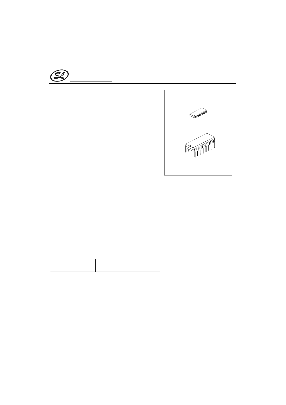
SC5260-R4 (S) 16 Pins, DIP (SO)
SC5260-R2 (S) 16 Pins, DIP (SO)
APPLICATIONS
* Home/Car Security System
* Garage Door Controller
* Remote Fan Controller
* Remote Control Toys
SC5260
SOP-16
DIP-16
HANGZHOU SILAN MICROELECTRONICS JOINT-STOCK CO.,LTD
Rev: 1.0 2000.12.31
1
Page 2
Silan
Semiconductors
BLOCK DIAGRAM
SC5260
A0
A1
A2
A3
A4
A5
A6
A7
A8/D3
A9/D2
D1
D0
PIN CONFIGURATION
1
A0
2
A1
3
A2
4
A3
5
A4
ADDRESS
/DATA
SC5260-R4
SYSTEM
TIMING
CONTROL
LOGIC
CODE
GENERATION
OSC OSC
DOUT
16
CC
V
15
DOUT
OSC
14
D0
13
D1
12
A0
A1
A2
A3
A4
1
2
3
4
5
SC5260-R2
16
CC
V
15
DOUT
OSC
14
D0
13
D1
12
A5
A6
A7
6
7
8
D2
11
D3
10
V
9
SS
A5
A6
A7
6
7
8
11
10
9
ABSOLUTE MAXIMUM RATINGS
Characteristic Symbol Value Unit
Supply Voltage V
Input/Output Voltage VIN,V
Maximum Power Dissipation P
CC
OUT
a
-0.3 ~ +6.0 V
-0.3V ~ VCC+0.3V V
500 mW
Operating Temperature Topr -30 ~ +70
Storage Temperature Tstg -40 ~+125
HANGZHOU SILAN MICROELECTRONICS JOINT-STOCK CO.,LTD
2
A9
A8
V
SS
Rev: 1.0 2000.12.31
°C
°C
Page 3
Silan
Semiconductors
ELECTRICAL CHARACTERISTICS
Parameter Symbol Test conditions Min Typ Max Unit
Supply Voltage V
Stand-by Current I
DOUT Output Driving Current I
DOUT Output Sinking Current I
Operation Current Iop
OH
OL
CC
VCC=3V OSC stops
sb
All input pins open
VCC=3V, VOH=1.5V
V
CC
VCC=3V, VOH=1.5V
V
CC
V
CC
V
CC
=6.0V, VOH=3.0V
=6.0V, VOH=3.0V
=1.8V
=6.0V
1.8 6.0 V
0.2 0.5 0.8
2.5
4.6
0.01
0.50
PIN DESCRIPTION
Pin No. Symbol I/O Description
1~8 A0~A7 I Code Address Pin Nos.0~7
These eight tri-state pins ate detected by SC5260 to determine the
encoded waveform bit0~bit7. Each bit can be set to “0”, “1”, or
“f”(floating).
10~11 A8/D3~A9/D2 I/PL* Code Address pin Nos.8~9/Data Pin Nos.3~2.
These two tri-state pins are detected by SC5260 to determine the
encoded waveform bit8~bit9. When these pins ate used as address
pins (as in SC5260-R2), they can be set to “0”, “1”, or “f” (floating).
When these pins are used as data pins (as in SC5260-R4), they can
only be set to “0” or “1”.
12~13 D1, D0 I/PL Data Pin Nos. 1~0. These pins can only be set to “0” or “1”.
14 OSC I Oscillator Pin A resistor connected between the OSC Pin and the VCC
determines the fundamental frequency of the SC5260.
15 DOUT O Data Output Pin. The encoded waveform is serially outputted to this
pin. When SC5260 is not transmitting, DOUT outputs low (VSS)
voltage.
16 VCC Positive Power Supply
9 VSS Negative Power Supply
Note: PL -- Pull-low Resistor is connected internally
PL* -- If those two pins are used as Data Pins (SC5260-R2), pull-low resistor is connected internally;
otherwise, no pull-low resistor is connected.
SC5260
10
12
µA
mA
mA
mA
HANGZHOU SILAN MICROELECTRONICS JOINT-STOCK CO.,LTD
Rev: 1.0 2000.12.31
3
Page 4

Silan
Semiconductors
FUNCTIONAL DESCRIPTION
SC5260 encodes the code address and data set at A0~A7, A8/D3, A9/D2, D1 and D0 into a special waveform
and outputs it to the DOUT when any of the data pins is tied to high. This waveform is fed to the RF Modulator for
transmission. The transmitted radio frequency is received by the RF demodulator and reshaped into the special
waveform. SC5270 (or SC5272) is then used to decode the waveform and set the corresponding output pin(s).
Thus completing a remote control encoding and decoding function.
1. RF Operation
1) Code Bits
A Code Bits is the basic component of the encoded waveform, and can be classified as either an
(Address/Data) Bit or a SYNC (Synchronous) Bit.
•
Address/Data (AD) Bit Waveform
An AD Bit can be designated as Bit “0”, “1”, or “f” if it is in low, high or floating state respectively. One bit
waveform consists of 2 pulse cycles. Each pulse cycle has 512 oscillating clock periods. For further details, please
refer to the diagram below:
¢
Osc
Bit "0"
128
¢
Bit "1"
384
Bit "f"
Floating
Where: α = Oscillating Clock Period
1 bit = 1024
¢
128
¢
¢
SC5260
AD
•
Synchronous (SYNC.) Bit Waveform
The Synchronous Bit Waveform is 4 bits long with 1/8 bit width pulse. Please refer to the diagram below:
1/8bitwidth=128
4 bit width = 4096
Note: 1 bit = 1024
¢
¢
¢
HANGZHOU SILAN MICROELECTRONICS JOINT-STOCK CO.,LTD
Rev: 1.0 2000.12.31
4
Page 5

Silan
Semiconductors
2) Code Word
A group of Code Bits is called a Code Word. A Code Word consists of 12 AD bits followed by one Sync Bit. The
12 AD bits are determined by the corresponding states of A0~A7, A8/D3, A9/D2, D1 and D0 pins at the time of
transmission. When the Data Type of SC5260 is used, the address bits will decrease accordingly.
For example: In the 4-Data Type where the address has eight (8) bits, the transmitting format is:
8 Address Bits 4DataBits Sync. Bit
SC5260 has a maximum of ten (10) Address Bits. The following diagram shows the code bits with their
corresponding pins.
First Bit Transmitted
SC5260
A0 A1 A2 A3 A4 A5 A6 A7
One Complete Code Word
A8/D3A9/
D2
D1 D0 SYNC BIT
2 Data: A0 A1 A2 A3 A4 A5 A6 A7 A8 A9 D1 D0 Sync Bit
4 Data: A0 A1 A2 A3 A4 A5 A6 A7 D3 D2 D1 D0 Sync Bit
The Code Bits A0~A7, A8/D3, A9/D2, D1 and D0 are determined by the states set at these pins. For example,
when the A0 (Pin No.1) is set to “1” (VCC), the Code Bit A0 is synthesized as “1” bit. In the same manner, when it
(A0 Pin) is set to “0” (VSS) or left floating, the Code Bit A0 is synthesized as a “0” or “f” bit respectively.
When SC5260 detects “1” on any of the Data Pins, it outputs a Code Word at DOUT. If the Data Pin is still in
high state (“1”) the time the Code Word transmission ends, SC5260 outputs the same Code Word. Please refer
to the diagram below:
DATA PIN
DOUT
1 CodeWord 1 Code Word 1 Code Word 1 Code Word
HANGZHOU SILAN MICROELECTRONICS JOINT-STOCK CO.,LTD
Rev: 1.0 2000.12.31
5
Page 6

Silan
Semiconductors
3) Single Resistor Oscillator
The built-in oscillator circuitry of SC5260 allows a precision oscillator to be constructed by connecting an external
resistor between OSC and VCC pins. For SC5270 (or SC5272) to decode correctly the received waveform, the
oscillator frequency of SC5270 (or SC5272) must be 1/16~4 (or 1/16~1/4) times that of the transmitting SC5260.
The typical oscillator frequency of SC5270, and SC5272 are shown below:
Encoder (SC5260) OSC Frequency Decoder (SC5270) OSC Frequency
500
180
400
300
250
200
Frequency (KHz)
100
12345678910
Voltage (Volts)
Decoder (SC5272) OSC Frequency
1000
R=820K
R=1M
R=2M
R=100K
160
140
120
100
80
Frequency (KHz)
60
40
20
0
2 4 6 8 10 12
0
Voltage (Vcc)
SC5260
OSC Resistor = 510K Ohms
OSC Resistor = 1.0M Ohms
OSC Resistor = 1.2M Ohms
OSC Resistor = 2.2M Ohms
100
Frequency (KHz)
10
369
Voltage
12 15
R=240K
R=510K
R=1M
R=2M
Suggested oscillator resistor values are shown below.
SC5260 SC5270 SC5272
820k
â
510k
â
1M
â
1M
â
620k
â
1.2M
â
2M
â
1.2M
â
2.2M
â
HANGZHOU SILAN MICROELECTRONICS JOINT-STOCK CO.,LTD
Rev: 1.0 2000.12.31
6
Page 7

Silan
Semiconductors
OPERATION FLOWCHART
Power ON
Stand-byMode
SC5260
APPLICATION CIRCUIT
Vcc
16 15 14 13 12 11 10 9
820K
NO
1WordofAddress
/Data Transmitted
NO
SC5260-R4
Data Pin(s) still
Data Pin(s)
in HIGH State
YES
in HIGH State
YES
10
47K
87654321
H
5p 5p
HANGZHOU SILAN MICROELECTRONICS JOINT-STOCK CO.,LTD
Rev: 1.0 2000.12.31
7
Page 8

Silan
Semiconductors
PACKAGE OUTLINE
DIP-16-300-2.54 UNIT: mm
2.54
SC5260
0.25
6.40
3.51
19.4
1.50
0.46
7.62
15 degree
5.083.30
SOP-16-225-1.27 UNIT: mm
0.41
3.95
6.00
5.72
1.27
HANGZHOU SILAN MICROELECTRONICS JOINT-STOCK CO.,LTD
10.20
9.80
1.95
Rev: 1.0 2000.12.31
8
 Loading...