

Page 1
SHUNT REGULATOR WITH OPEN
COLLECTOR OR OUTPUT
SC4431
PRELIMINARY - September 11, 2000
TEL:805-498-2111 FAX:805-498-3804 WEB:http://www.semtech.com
DESCRIPTION
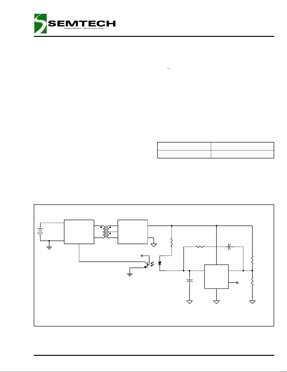
The SC4431 is a four terminal device for regulating an
isolated power supply with very low output voltage.
It is intended to be used as a replacement for three terminal shunt regulators such as SC431L where the output voltage is too low for them to function in conjunction with an opto-isolator. It achieves this by having
seperate supply and output pins, allowing the output to
sink current at voltages as low as 0.2V, while the supply pin still has sufficient voltage for the device to function. In this way, allowing for a 1.6V drop through an
opto-isolator diode, regulation down to 1.8V out can be
achieved.
The SC4431 shunt regulator is available with three initial reference voltage accuracies (0.5%, 1.0% and
2.0%) in the space saving 5-lead SOT-23 package.
The three voltage tolerances allow the designer the
opportunity to select the proper cost/tolerance for their
application.
TYPICAL APPLICATION CIRCUIT
FEATURES
•= Trimmed bandgap design - initial accuracies to
0.5%
+
•= 40mA drive capability
•= Wide supply voltage range - 1.5V to 15V
•= Low supply current - typically 110µA
•= Full industrial temperature range
APPLICATIONS
•= Opto driver for very low output voltage isolated
power supplies
ORDERING INFORMATION
Part Number
SC4431CSK-X.TR SOT-23-5
Notes:
(1) Where “-X” denotes initial reference voltage tolerance. Available options are ±0.5% (-.5), ±1% (-1) and
±2% (-2).
(2) Only available in tape and reel packaging. A reel
contains 3000 devices.
(1)(2)
Package
VIN
Primary Side
Controller
T1
Secondary Side
Rectification
and Filtering
R1
U1
4N25
R2
5.1k
U2 SC4431
C2
22nF
1
VCC
GND
2
2V OUT
C1
33nF
45
REFOUT
3
NC
R3
6.34k
R4
10k
2V Output Isolated Power Supply
1
© 2000 SEMTECH CORP. 652 MITCHELL ROAD NEWBURY PARK CA 91320
Page 2

SHUNT REGULATOR WITH OPEN
SC4431
COLLECTOR OR OUTPUT
PRELIMINARY - September 11, 2000
ABSOLUTE MAXIMUM RATINGS
Parameter Symbol Maximum Units
Input Supply Voltage V
Output Voltage V
Reference Voltage V
Continuous Output Current I
Reference Input Current I
Operating Ambient Temperature Range T
Operating Junction Temperature Range T
Storage Temperature Range T
Thermal Impedance Junction to Ambient
Thermal Impedance Junction to Case
Power Dissipation at T
= 25°C P
A
θ
Lead Temperature (Soldering) 10 seconds T
CC
OUT
REF
OUT
REF
STG
θ
JA
JC
LEAD
A
J
D
-0.5 to +16 V
-0.5 to V
CC
V
-0.5 to +4 V
40 mA
5mA
-40 to +85 °C
-40 to +150 °C
-65 to +150 °C
256 °C/W
81 °C/W
475 mW
300 °C
ESD Rating (Human Body Model) ESD 2 kV
ELECTRICAL CHARACTERISTICS
Unless specified, TA = 25°C, VCC = 2V, I
Parameter Symbol Test Conditions MIN TYP MAX Units
VCC
= 2mA. Values in bold apply over ful l operating temperature range.
OUT
Input Supply Voltage V
Input Supply Current I
Off State Input Supply Current I
CC(OFF)
REF
Reference Voltage V
Change in V
in V
CC
Change in V
in I
OUT
due to change VCC = 1.5V to 15V 8 15 mV
REF
due to change I
REF
dV
dV
dV
dI
CC
CC
REF
REF
CC
REF
OUT
1.5 15
V
REF
V
= 1.187V, V
REF
SC4431-.5, V
= V
OUT
= 2V 65 100 µA
OUT
REF
= V
OUT
1.219 1.224 1.231 V
110
1.207 1.243
SC4431-1, V
REF
= V
OUT
1.212 1.224 1.236 V
1.200 1.250
SC4431-2, V
REF
= V
OUT
1.200 1.224 1.250 V
1.187 1.261
= 0.1mA to 40mA 8 28 mV
OUT
200
150
20
36
V
µA
2
© 2000 SEMTECH CORP. 652 MITCHELL ROAD NEWBURY PARK CA 91320
Page 3
SHUNT REGULATOR WITH OPEN
SC4431
COLLECTOR OR OUTPUT
PRELIMINARY - September 11, 2000
ELECTRICAL CHARACTERISTICS (Cont.)
Unless specified, TA = 25°C, VCC = 2V, I
Parameter Symbol Test Conditions MIN TYP MAX Units
REF (Cont.)
= 2mA. Values in bold apply over ful l operating temperature range.
OUT
Reference Input Current I
OUT
Saturation Voltage V
Off State Output Current I
OUT(OFF)
REF
OUT(SAT)
0.1mA ≤ I
I
= 5mA, ICC = 500µA 50 75 mV
OUT
V
= 1.261V, I
REF
V
= 1.187V, V
REF
≤ 10mA
OUT
= 40mA 275 300 mV
OUT
= 2V 0.5 1 µA
OUT
0.3 0.5 µA
1.0
100
400
10
3
© 2000 SEMTECH CORP. 652 MITCHELL ROAD NEWBURY PARK CA 91320
Page 4

PRELIMINARY - September 11, 2000
BLOCK DIAGRAM
SHUNT REGULATOR WITH OPEN
COLLECTOR OR OUTPUT
SC4431
PIN CONFIGURATION
SOT-23 -5 Lead (Top View)
PIN DESCRIPTION
Pin Pin Name Pin Function
1 VCC This is the input supply pin for the IC.
2 GND Logic and power ground.
3 NC No connection.
4 REF This is connected to the non-inverting input of the error amplifier.
5 OUT This is the output pin of the device, essentially an open collector.
4
© 2000 SEMTECH CORP. 652 MITCHELL ROAD NEWBURY PARK CA 91320
Page 5

PRELIMINARY - September 11, 2000
DEVICE OUTLINE - SOT-23-5
SHUNT REGULATOR WITH OPEN
COLLECTOR OR OUTPUT
SC4431
LAND PATTERN - SOT-23-5
ECN 00-1315
5
© 2000 SEMTECH CORP. 652 MITCHELL ROAD NEWBURY PARK CA 91320
 Loading...