

Datasheet SC1566I5M-1.8.TR, SC1566I5M-2.5.TR, SC1566I5T, SC1566I5T-1.8, SC1566I5T-2.5 Datasheet (Semtech Corporation)
...Page 1
1 www.semtech.com
SC1566
Very Low Dropout
3.0 Amp Regulator With Enable
POWER MANAGEMENT
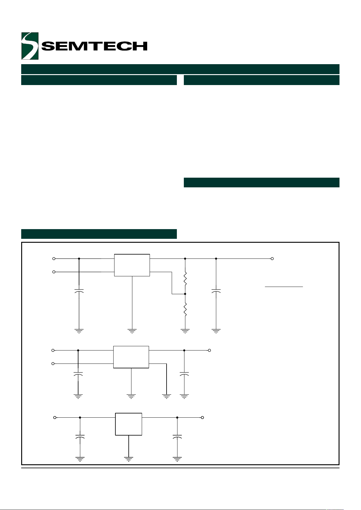
VIN
ENABLE
VO = See equation below
C1
C2
R1
R2
U1
SC1566I5T-2.5
1
2
3
4
5
VIN
EN
GND
ADJ
VO
VIN
ENABLE
VO = 2.5V
C1
C2
U1
SC1566I5T-2.5
1
2
3
4
5
VIN
EN
GND
ADJ
VO
VIN VO = 1.8V
C1
C2
U1
SC1566IT-1.8
1
2
3
VIN
GND
VO
Revision 1, January 2001
The SC1566 is a high performance positive voltage
regulator designed for use in applications requiring very
low dropout voltage at up to 3 Amps. Since it has
superior dropout characteristics compared to regular
LDOs, it can be used to supply 2.5V on motherboards or
2.8V on peripheral cards from the 3.3V supply thus
allowing heat sink size reduction or elimination.
Additionally, the five pin versions of SC1566 have an
enable pin, to further reduce power dissipation while shut
down. The SC1566 provides excellent regulation over
variations in line, load and temperature.
The SC1566 is available as three terminal fixed output
voltage and five terminal fixed or adjustable output
voltage devices with enable. Two package options are
available: TO-263 and TO-220.
u 350mV dropout @ 3A
u Adjustable output from 1.2V to 4.8V
u 2.5V and 1.8V options (5 pin parts also adjustable
externally using resistors)
u Over current and over temperature protection
u Enable pin
u 10µA quiescent current in shutdown
u Low reverse leakage (output to input)
u Full industrial temperature range
u TO-220 and TO-263 packages
u Battery powered systems
u Motherboards and notebook computers
u Peripheral cards
u Network cards
u Set top boxes
u Medical equipment
Volts
R2
R2)(R1 1.200VO+
=
FeaturesDescription
Applications
Typical Application Circuits
(1)(2)
Notes:
(1) Maximum VO setpoint for 1.8V parts = 5.4V
(2) This device is designed to operate with
ceramic input and output capacitors
Page 2
2ã 2001 Semtech Corp. www.semtech.com
SC1566
POWER MANAGEMENT
retemaraP lobmySxaMstinU
egatloVtupnI V
NI
5.5V
noitapissiDrewoP P
D
detimiLyllanretnIW
tneibmAotnoitcnuJecnatsiseRlamrehT
)362-OT(MI6651CS
)022-OT(TI6651CS
q
AJ
06
05
W/C°
esaCotnoitcnuJecnatsiseRlamrehT
)362-OT(MI6651CS
)022-OT(TI6651CS
q
CJ
3
3
W/C°
egnaRerutarepmeTtneibmAgnitarepO T
A
58+ot04-C°
egnaRerutarepmeTnoitcnuJgnitarepO T
J
051+ot04-C°
egnaRerutarepmeTegarotS T
GTS
051+ot56-C°
.ceS01)gniredloS(erutarepmeTdaeL T
DAEL
003C°
)ledoMydoBnamuH(gnitaRDSE V
DSE
2Vk
retemaraPlobmySsnoitidnoCtseTniMpyTxaMstinU
NIV
egnaRegatloVylppuSV
NI
2.25.5 V
tnerruCtnecseiuQI
Q
V
NI
V3.3=57.0 57.1 Am
V
NI
V,V5.5=
NE
V0=01 53 Aµ
OV
egatloVtuptuO
)1(
V
O
VNIV=
O
I,V7.0+
O
Am01=%1-VO%1+V
)egatloVdexiFlanretnI(
%2-%2+
noitalugeReniL
)1(
GER
)ENIL(
V
NI
V(=
O
I,V5.5ot)V52.0+
TUO
Am01=530.0 3.0 %
noitalugeRdaoL
)1(
GER
)DAOL(
VNIV=
O
V7.0+2.0 4.0 %
egatloVtuoporD
)2()1(
V
D
I
O
Am01=15Vm
01
I
O
Am005=57001Vm
051
Absolute Maximum Ratings
Electrical Characteristics
Unless specified: VEN = VIN. Adjustable Option (V
ADJ
> V
TH(ADJ)
): VIN = 2.2V to 5.5V and IO = 10µA to 3A.
Fixed Options (V
ADJ
= GND): VIN = (VO + 0.7V) to 5.5V and IO = 0A to 3A. Values in bold apply over the full operating temperature range.
Page 3
3ã 2001 Semtech Corp. www.semtech.com
SC1566
POWER MANAGEMENT
Notes:
(1) Low duty cycle pulse testing with Kelvin connections required.
(2) Defined as the input to output differential at which the output voltage drops to 1% below the value
measured at a differential of 0.7V.
(3) Required to maintain regulation. Voltage set resistors R1 and R2 are usually utilized to meet this
requirement. Adjustable versions only.
(4) Guaranteed by design.
(5) When V
ADJ
exceeds this threshold, the Sense Select switch disconnects the internal feedback chain from
the error amplifier and connects V
ADJ
instead.
retemaraPlobmySsnoitidnoCtseTniMpyTxaMstinU
).tnoC(OV
egatloVtuoporD
)2()1(
I
O
A5.1=002003Vm
004
I
O
A3=053054Vm
006
tnerruCdaoLmuminiM
)3(
I
O
VNIV=
O
V7.0+101 Aµ
timiLtnerruCI
LC
0.3 5.4 5.6 A
JDA
egatloVecnerefeR
)1(
V
FER
V
NI
V,V2.2=
JDA
V=
TUOI,O
Am01=881.1002.1212.1V
671.1422.1
tnerruCniPtsujdA
)4(
I
JDA
V
JDA
V=
FER
01 05 An
dlohserhTniPtsujdA
)5(
V
)JDA(HT
01.0 02.0 04.0 V
NE
tnerruCniPelbanEI
NE
V
NE
V,V0=
NI
V3.3=5.1 01 Aµ
dlohserhTniPelbanEV
HI
V
NI
V3.3= 8.1 V
V
LI
V
NI
V3.3= 4.0
noitcetorPerutarepmeTrevO
levelpirThgiHT
IH
571C°
siseretsyHT
TSYH
01C°
Electrical Characteristics (Cont.)
Unless specified: VEN = VIN. Adjustable Option (V
ADJ
> V
TH(ADJ)
): VIN = 2.2V to 5.5V and IO = 10µA to 3A.
Fixed Options (V
ADJ
= GND): VIN = (VO + 0.7V) to 5.5V and IO = 0A to 3A. Values in bold apply over the full operating temperature range.
Page 4
4ã 2001 Semtech Corp. www.semtech.com
SC1566
POWER MANAGEMENT
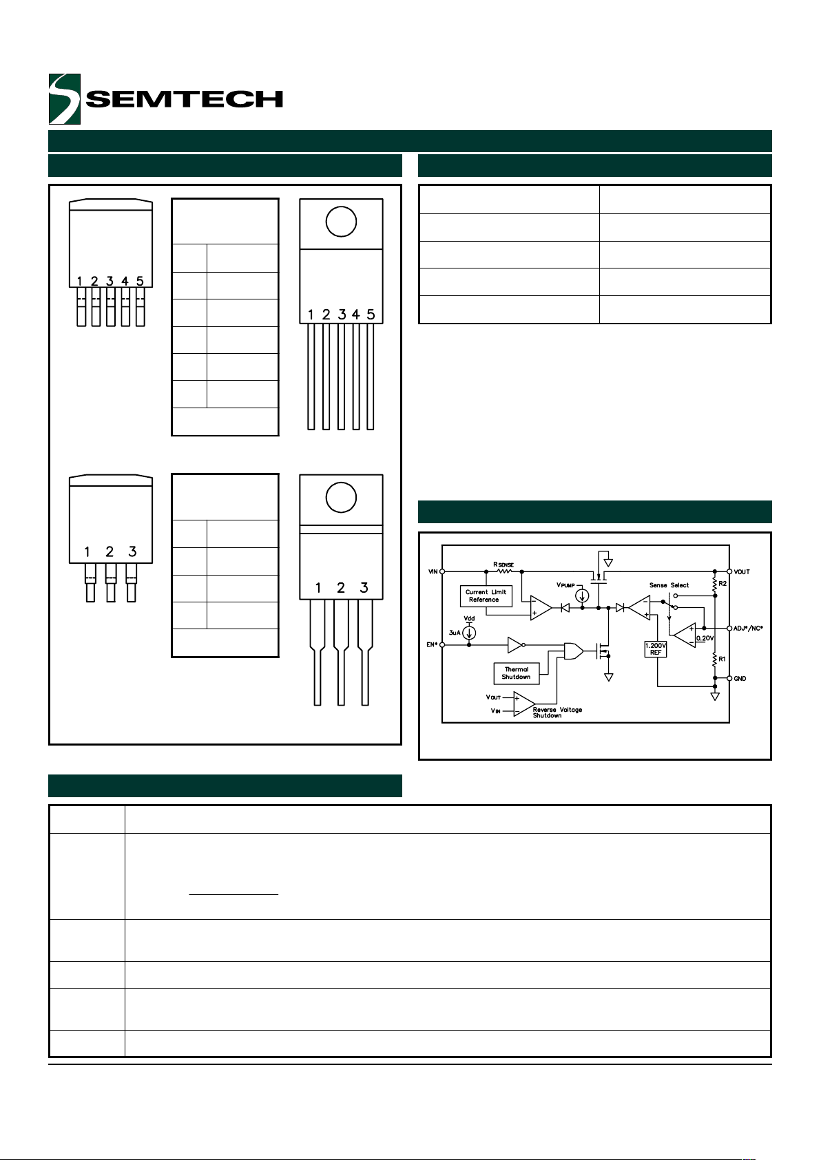
emaNniPnoitpicseDniP
JDA lanretxefI.srotsiserkcabdeeflanretniehtybtestahtotegatlovtuptuoehtstes,dednuorgnehw,nipsihT
:)1egapnostiucriCnoitacilppAeeS(eblliwegatlovtuptuoeht,desuerasrotsiserkcabdeef
NE fonoitcarfaottnerructnecseiuqehtgnicuder,fforotalugerehtsnrutV4.0wolebnipsihtgnilluP.tupnIelbanE
.desugniebtonfiNIVottcennoC.nepotfelsinipsihtfidelbaneeblliwecivedehT.eulavgnitareposti
DNG .gniknistaehrof)DNGotdetcennocyllacirtcele(batehtesU.dnuorgecnerefeR
NIV muminiM.V5.5dna)V7.0+OV(neewtebebtsumnipsihtottupnieht,daollluftanoitalugerroF.egatlovtupnI
.V2.2=NIV
OV.ecivedehtfotuptuorewopehtsinipsihT
Volts
R2
R2)(R11.200VO+
=
Pin Descriptions
Pin Configurations
Note:
(1) 3-pin versions are fixed output
voltage only.
NIP-56651CS
snoisreV
niPnoitcnuF
1NIV
2NE
3DNG
4JDA
5OV
DNGSIBAT
Ordering Information
TO-263-5
TO-220-5
TO-263-3
NIP-36651CS
snoisreV
niPnoitcnuF
1NIV
2DNG
3OV
DNGSIBAT
TO-220-3
Notes:
(1) Where -X.X denotes voltage options. Available
voltages are: 2.5V and 1.8V.
(2) Output voltage can be adjusted using external
resistors, see Pin Descriptions below.
(3) Only available in tape and reel packaging. A reel
contains 800 devices.
(6) Only available in tube packaging. A tube contains 50
devices.
eciveD
)1(
egakcaP
RT.X.X-MI6651CS3-362-OT
)3(
RT.X.X-M5I6651CS
)2(
5-362-OT
)3(
X.X-TI6651CS3-022-OT
)4(
X.X-T5I6651CS
)2(
5-022-OT
)4(
Block Diagram
* 5 lead versions only
Page 5
5ã 2001 Semtech Corp. www.semtech.com
SC1566
POWER MANAGEMENT
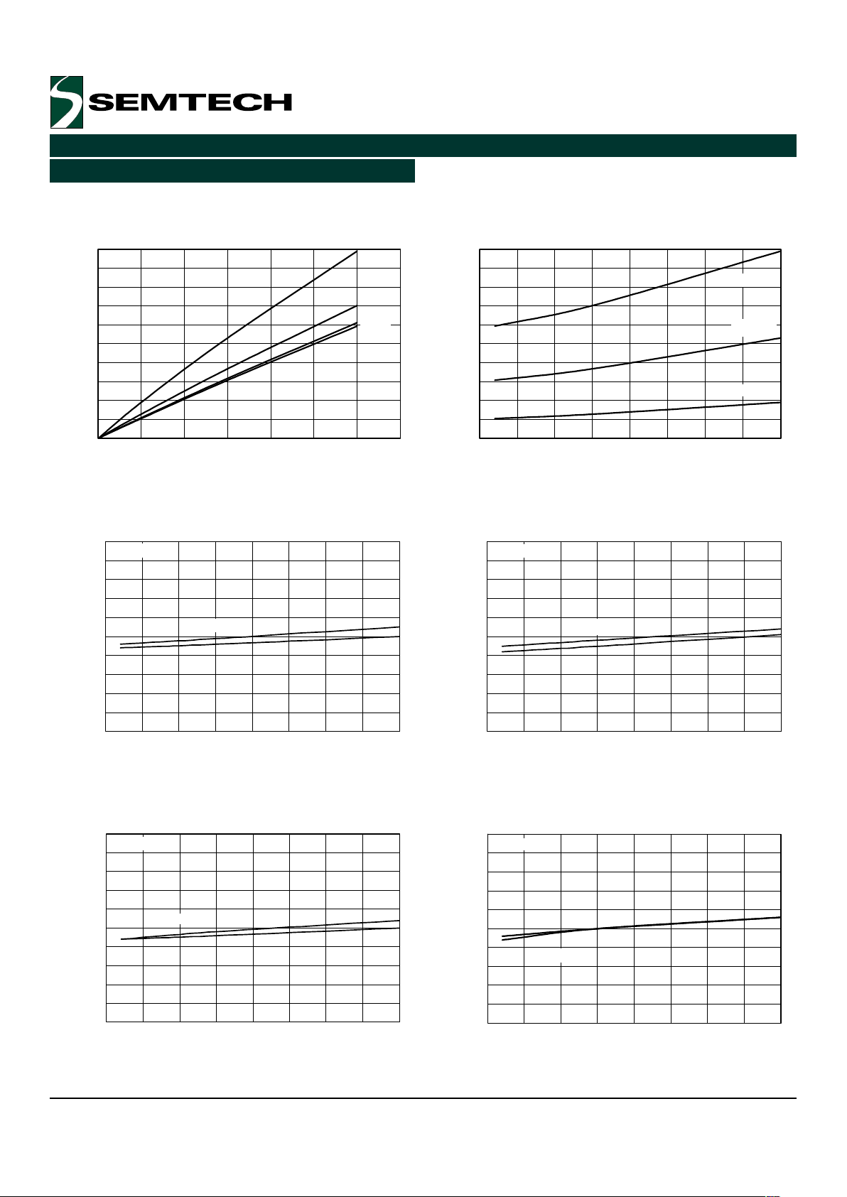
Typical Characteristics
Dropout Voltage vs. Output Current
vs. Junction Temperature
Dropout Voltage vs. Junction
Temperature vs. Output Current
Output Voltage (2.5V) vs. Junction
Temperature vs. Output Current
Output Voltage (2.5V) vs. Junction
Temperature vs. Output Current
Reference Voltage vs. Junction
Temperature vs. Output Current
Reference Voltage vs. Junction
Temperature vs. Output Current
0
50
100
150
200
250
300
350
400
450
500
0.0 0.5 1.0 1.5 2.0 2.5 3.0 3.5
I
O
(A)
V
D
(mV)
0°C
-40°C
150°C
25°C
0
50
100
150
200
250
300
350
400
450
500
-50 -25 0 25 50 75 100 125 150
T
J
(°C)
V
D
(mV)
IO = 0.5A
I
O
= 1.5A
I
O
= 3A
2.450
2.460
2.470
2.480
2.490
2.500
2.510
2.520
2.530
2.540
2.550
-50 -25 0 25 50 75 100 125 150
T
J
(°C)
VO (V)
IO = 3A
I
O
= 10mA
VIN = 3.2V
2.450
2.460
2.470
2.480
2.490
2.500
2.510
2.520
2.530
2.540
2.550
-50 -25 0 25 50 75 100 125 150
T
J
(°C)
VO (V)
IO = 3A
I
O
= 10mA
VIN = 5.5V
1.175
1.180
1.185
1.190
1.195
1.200
1.205
1.210
1.215
1.220
1.225
-50 -25 0 25 50 75 100 125 150
T
J
(°C)
V
REF
(V)
VIN = 2.2V
I
O
= 10mA
I
O
= 3A
1.175
1.180
1.185
1.190
1.195
1.200
1.205
1.210
1.215
1.220
1.225
-50 -25 0 25 50 75 100 125 150
T
J
(°C)
V
REF
(V)
VIN = 5.5V
I
O
= 10mA
I
O
= 3A
Page 6
6ã 2001 Semtech Corp. www.semtech.com
SC1566
POWER MANAGEMENT
Introduction
The SC1566 is intended for applications such as
graphics cards where high current capability and very low
dropout voltage are required. It provides a very simple,
low cost solution that uses very little pcb real estate and
typically does not require a heatsink. Additional features
include an enable pin to allow for a very low power
consumption standby mode, and a fully adjustable
output (5-pin versions).
Component Selection
Input capacitor: a 4.7µF or 10µF ceramic capacitor is
recommended. This allows for the device being some
distance from any bulk capacitance on the rail.
Additionally, input droop due to load transients is reduced,
improving load transient response. Additional capacitance
may be added if required by the application.
Output capacitor: a minimum bulk capacitance of 22µF,
along with a 0.1µF ceramic decoupling capacitor is
recommended. Increasing the bulk capacitance will
improve the overall transient response. The use of
multiple lower value ceramic capacitors in parallel to
achieve the desired bulk capacitance will not cause
stability issues. Although designed for use with ceramic
output capacitors, the SC1566 is extremely tolerant of
output capacitor ESR values and thus will also work
comfortably with tantalum output capacitors.
Applications Information
External voltage selection resistors (5-pin parts): the
use of 1% resistors, and designing for a current flow
³ 10µA is recommended to ensure a well regulated
output (thus R2 £ 120kW).
Thermal Considerations
The power dissipation in the SC1566 is approximately
equal to the product of the output current and the input
to output voltage differential:
()
OD
IVOUTVINP •−≈
The absolute worst-case dissipation is given by:
(
)
)MAX(Q)MAX()MAX(O)MIN()MAX()MAX(D
IVINIVOUTVINP •+•−=
For a typical scenario, VIN = 3.3V ± 5%, V
OUT
= 2.8V and
IO = 2.5A, therefore:
V
IN(MAX)
= 3.465V, V
OUT(MIN)
= 2.744V and I
Q(MAX)
= 1.75mA,
Thus P
D(MAX)
= 1.81W.
Using this figure, and assuming T
A(MAX)
= 85°C, we can
calculate the maximum thermal impedance allowable to
maintain TJ £ 150°C (see page 7):
Typical Characteristics (Cont.)
Quiescent Current vs.
Junction Temperature
Off-State Quiescent Current vs.
Junction Temperature
600
610
620
630
640
650
660
670
680
690
700
-50 -25 0 25 50 75 100 125 150
T
J
(°C)
I
Q
(µA)
VIN = 3.3V
0
2
4
6
8
10
12
-50 -25 0 25 50 75 100 125 150
T
J
(°C)
I
Q(OFF)
(µA)
VIN = 5.5V
Page 7
7ã 2001 Semtech Corp. www.semtech.com
SC1566
POWER MANAGEMENT
(
)
()
W/C33Rtherefore
,W/C0RandW/C3R
W/C36
81.1
85150
P
TT
R
)MAX)(AS(TH
)SC(TH)MAX)(CJ(TH
)MAX(D
)MAX(A)MAX(J
)MAX)(AJ(TH
°=
°=°=
°=
−
=
−
=
−
−−
−
Applications Information (Cont.)
This should be achievable for the TO-263 package using
pcb copper area to aid in conducting the heat away from
the device, such as a large (~2 squ. inch) pad connected
to the tab of the device. Internal ground/power planes
and air flow will also assist in removing heat. For higher
power dissipations it may be necessary to use a small
heatsink and the TO-220 package.
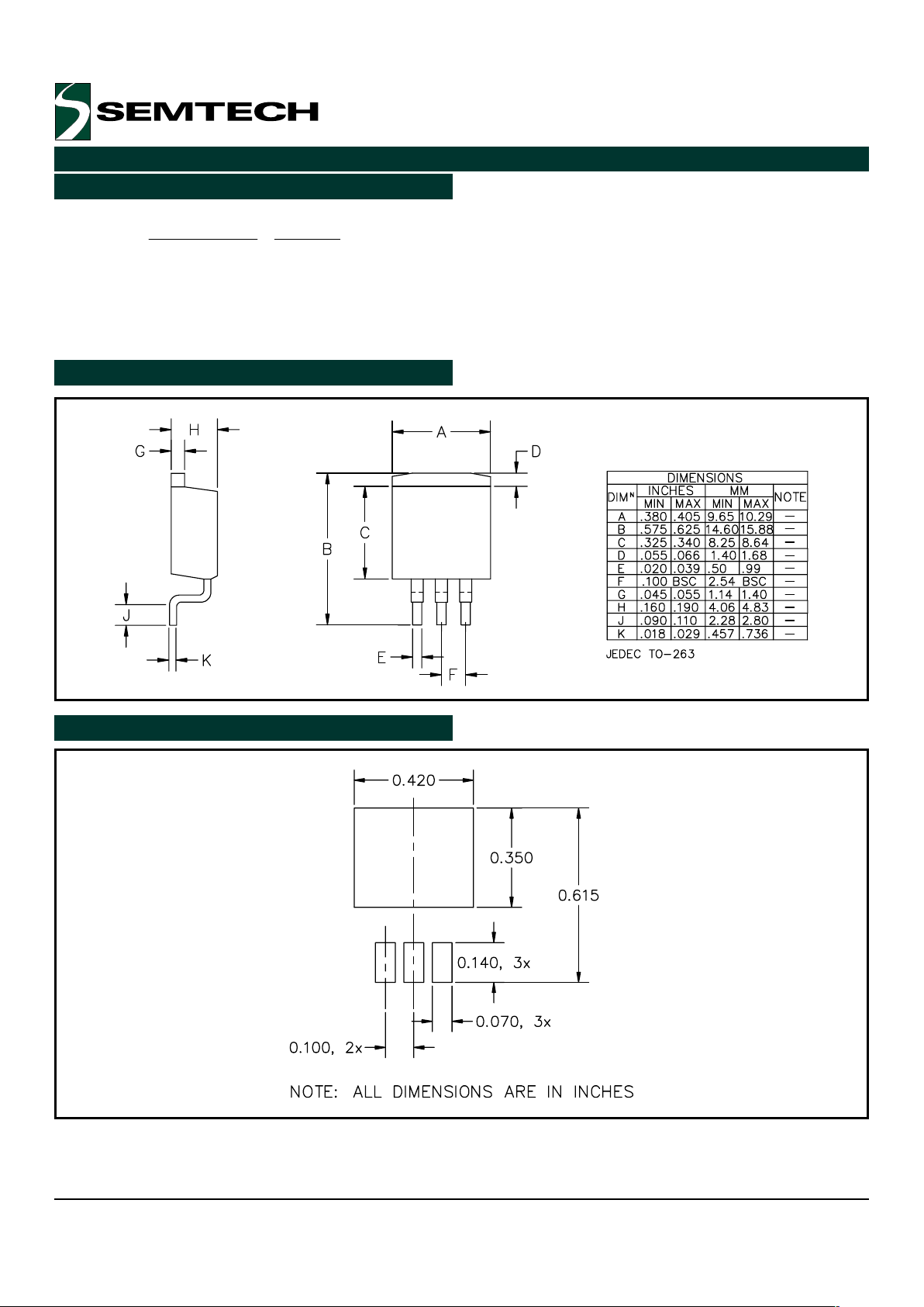
Outline Drawing - T0-263-3
Minimum Land Pattern - TO-263-3
Page 8
8ã 2001 Semtech Corp. www.semtech.com
SC1566
POWER MANAGEMENT
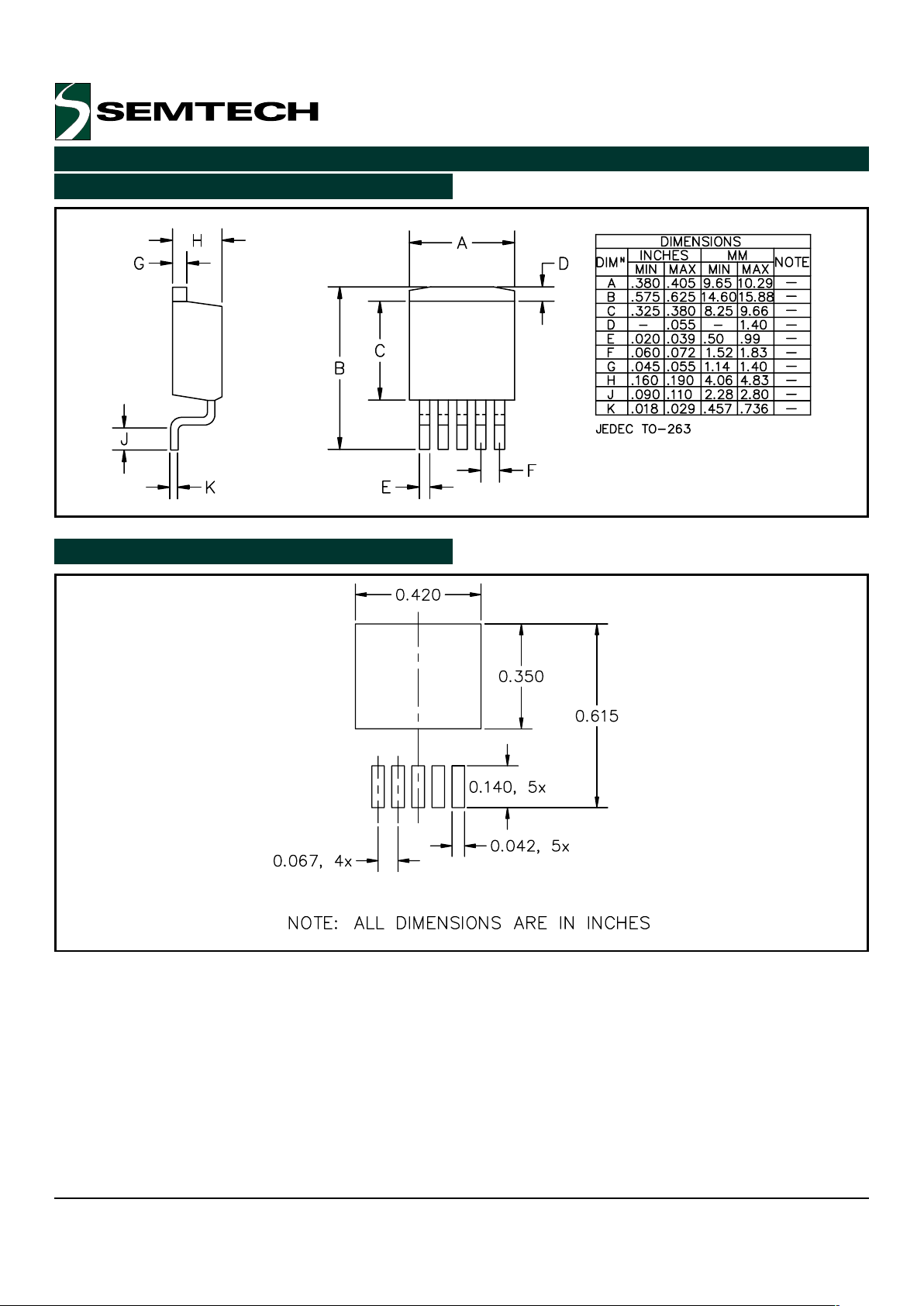
Outline Drawing - TO-263-5
Minimum Land Pattern - TO-263-5
Page 9
9ã 2001 Semtech Corp. www.semtech.com
SC1566
POWER MANAGEMENT
Semtech Corporation
Power Management Products Division
652 Mitchell Rd., Newbury Park, CA 91320
Phone: (805)498-2111 FAX (805)498-3804
Contact Information
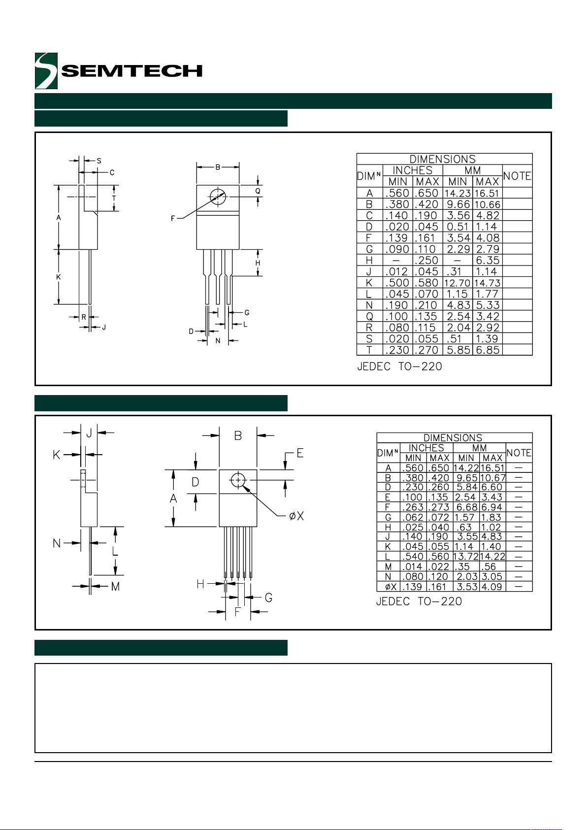
Outline Drawing - TO-220-3
Outline Drawing - TO-220-5
 Loading...