

Page 1
Copyright 1998 National Semiconductor Corp. 1 www.national.com
SC14402
Complete Baseband Processor for DECT Handsets
General Description
Preliminary document version 1.5.
The SC14402 is a 3.0 Volt CMOS chip optimized to handle
all the audio, signal and data processing needed within a
DECT handset. An ADPCM transcoder, a very low power
CODEC and Analog Frontend is integrated. Direct connections towards microphone and a (dynamical) loudspeaker are provided.
The SC14402 is designed such that it is compatible with
many radio interfaces.
A dedicated TDMA controller handles all physical layer
slot formats and radio control.
National Semiconductors standard CompactRISC
TM
CR16A 16 bit microcontroller with external ROM takes
care of all the higher protocol stack.
Features
■ Integrated DECT Baseband transceiver optimized for
GAP handsets according to ETS 300 175-2, 175-3 &
175-8.
■ 2.95 to 3.6 Volt operating voltage.
■ Very low power in active and paging mode.
■ Max 5V battery input.
■ Embedded 16 bit CompactRISC
TM
Micro Controller.
(CR16A) with programmable clock speeds.
■ ACCESSBUS
TM
or MICROWIRETM interfaces can be
handled.
■ 4 kByte on-chip Data Memory.
■ One full duplex ADPCM transcoder.
■ On-chip 14-bit linear CODEC.
■ 8 upto 38 dB gain differential microphone input buffer.
■ 100
Ω loudspeaker driver.
■ Software controlled gain on audio input and output.
■ On-chip gaussian Modulator.
■ Peak hold ADC for RSSI measurement.
■ Three general purpose inputs can be multiplexed on an
8 bit ADC with selectable ranges.
■ Advanced battery management unit
■ On board dedicated TDMA instruction co-processor
(DiP).
■ Eight programmable control signals for radio front end.
■ Serial interface to control radio front end circuitry.
■ Full support of all data formats.
________________________________________________________________________________________________
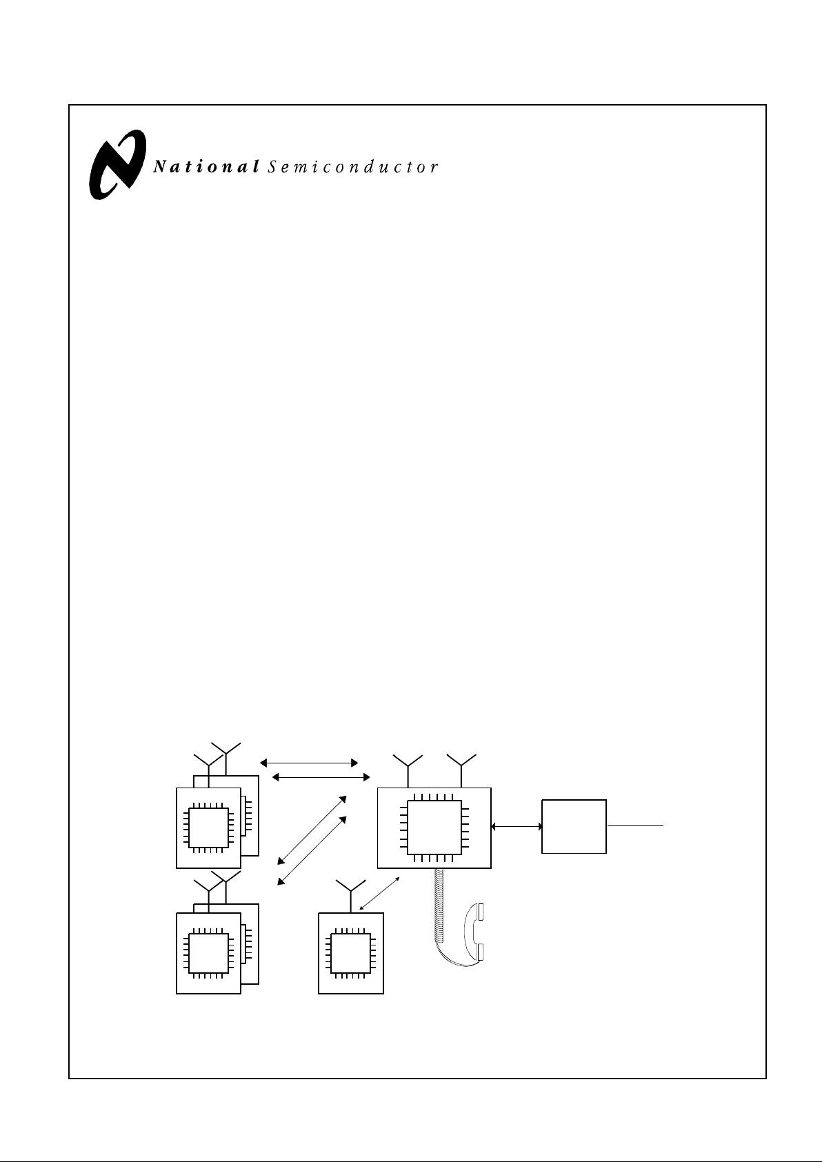
System Diagram
SC14401
SC14402
SC14401
4220030
SC14402
SC14402
SC14422
PSTN
ISDN
ISDN or
PSTN
Interface
PRELIMINARY
February 1998
SC14402 Complete Baseband Processor for DECT Handsets
ACCESSBUSTM, MICROWIRETM and CompactRISCTM are trademarks of National Semiconductor Corporation.
Page 2

Table of Contents
Copyright 1998 National Semiconductor Corp. 2
www.national.com
1.0CONNECTION DIAGRAM . . . . . . . . . . . . . . . . . . . . . . 3
2.0PIN DESCRIPTION . . . . . . . . . . . . . . . . . . . . . . . . . . .4
Page 3
Copyright 1998 National Semiconductor Corp. 3
www.national.com
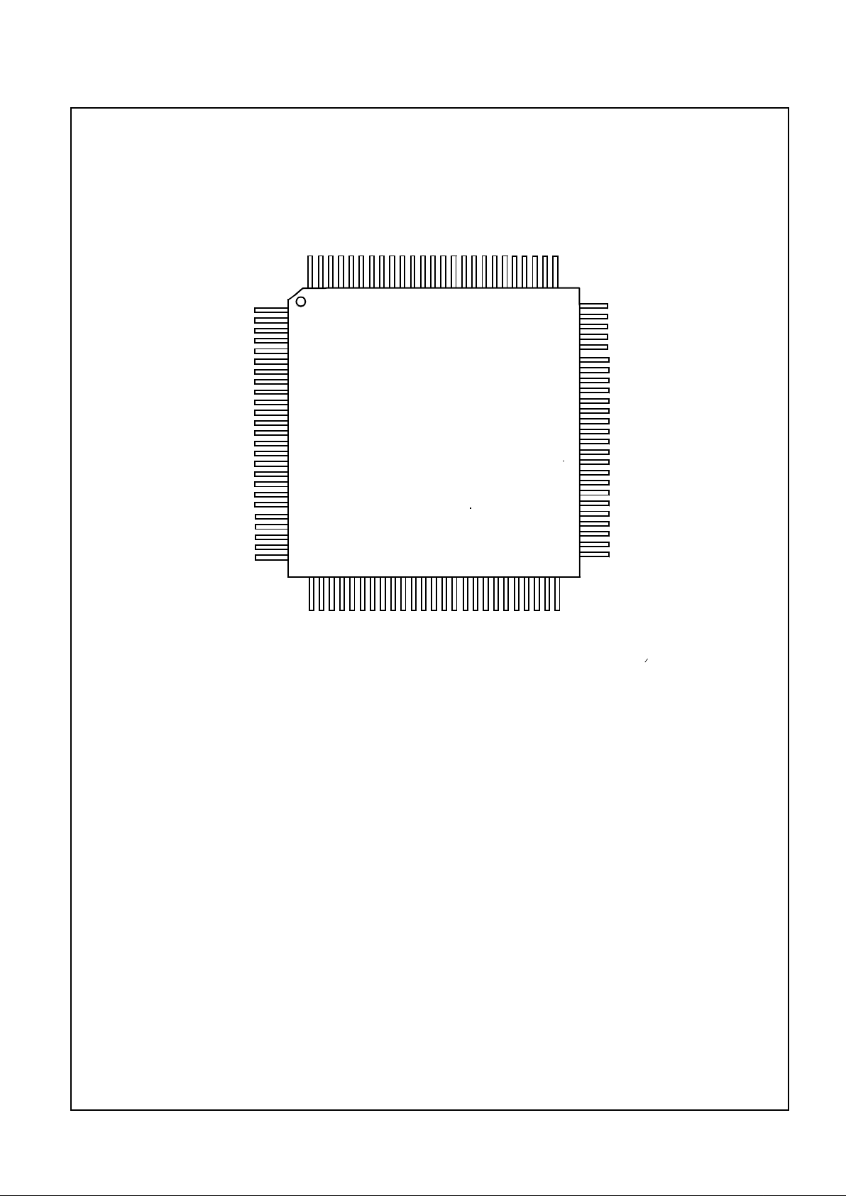
1.0Connection Diagram
Order Number SC14402VJG (Standard version)
Order Number SC14402CVJG (Standard version with improved clock recovery circuitry)
Order Number SC14402RVJG (‘R’ Version works with RTX-GAP Software)
Order Number SC14402CRVJG (‘R’ Version with improved clock recovery circuitry)
See NS Package Number VJG100A
B
u
z
z
e
r
+
B
u
z
z
e
r
-
LRS+
LRSVREFMICAGND
MIC+
AVD2
AVS2
VREF+
RST
N
57
64
56
63
55
62
69
54
61
68
53
60
67
52
59
66
51
58
65
P
2
[
1
]
P
2
[
2
]
P
2
[
3
]
P
2
[
4
]
CHARGE
V
B
A
T
1
21
22
23
24
25
35
45
26
36
46
27
37
472848
32
31
294930
50
344433
1
2
3
4
5
6
7
8
9
10
11
12
13
14
15
16
17
18
19
20
70
8079787776
75
74
73
72
71
89
98
99
100
889787968695859484938392829181
90
AD10
AD14
AD9
AD13
AD8
AD12
DAB7
DAB6
DAB5
DAB4
DAB3
DAB2
DAB1
DAB0
AD7
AD6
AD5
AD4
AD3
AD2
AD1
AD0
RFCLK
Vdd
Vss
CMPREF
AVS
AVD
RDI
RSSI
Xtal1
CAP
DAC
PD0
SO
PD1
SK
PD2
T
D
0
PD3
MEN1n
PD4
PD5
P
D
6
PD7
HOLD
AD11
AD15
AD16
MI/AD17
WRn
RDn
R
C
S
n
A
C
S
n
UTX
URX
P0[0]
P
1
[
0
]
P
0
[
4
]
P
1
[
4
]
P0[1]
P
1
[
1
]
P
0
[
5
]
P
1
[
5
]
P
1
[
2
]
P
0
[
6
]
P
1
[
6
]
P
0
[
3
]
P
1
[
3
]
P
0
[
7
]
P
1
[
7
]
P
2
[
0
]
V
S
S
V
D
D
I
N
T
n
7
I
N
T
n
0
I
N
T
n
1
I
N
T
n
2
I
N
T
n
3
I
N
T
n
4
I
N
T
n
5
I
N
T
n
6
SC14402
95208
Vdd
C
L
K
O
U
T
SCLK
Vss
3842413940
43
V
P
PTP
P
O
N
LKD
P
W
M
REG_ON
P2[5]
ADC
V
B
A
T
2
P0[2]
Page 4

Copyright 1998 National Semiconductor Corp. 4
www.national.com
2.0Pin Description
Table 1: Pin Description
PIN NAME TYPE DESCRIPTION
SCLK 1 5 OUTPUT (slope controlled). CR16A bus interface System CLocK output.
Vdd 2 Digital supply voltage
Vss 3 Digital ground.
PD
7..0
4-11 5 TRI-STATE OUTPUT. Power Down pins 7 to 0. PD7,6 have 12 mA drive.
RFCLK 12 5b OUTPUT (Slope controlled). 10 MHz clock output. Logic ‘0’ after reset or when dis-
abled.
MEN1n 13 5 OUTPUT. Load Enable. Can be synchronized to LKD input
SO 14 1 TRI-STATE OUTPUT. Serial data output.
SK 15 5 OUTPUT. Serial interface clock: 1.152 MHz
LKD 16 1 INPUT. LocK Detect input for synchronisation purposes.
RDI 17 analog INPUT. Received Data. It is programmable to invert this input.
CMPREF 18 analog INPUT. Comparator reference level. Internally a six bit DAC can be connected to
this pin to compensate for DC offsets.
RSSI 19 analog INPUT. 6-bit ADC input with peak hold circuitry. Activated on PD0 = low. If PD0 =
high the RSSI input will be discharged to ground.
AVD 20 Analog supply voltage
AVS 21 Analog ground
TDO 22 5/analog TRI-STATE OUTPUT. Transmit Data. Can be programmed to be inverted.
P0[0] or
UTX
23 2 INPUT/OUTPUT with selectable pull up resistor. General purpose memory
mapped I/O port bit. UART data output.
P0[1] or
URX
24 3 INPUT/OUTPUT with selectable pull down resistor. General purpose memory
mapped I/O port bit. UART data input.
P0[2] 25 2 INPUT/OUTPUT with selectable pull up resistor. General purpose memory
mapped I/O port bit. Can be switched to ADPCM/CODEC testpoints.
P0[3] 26 2 INPUT/OUTPUT with selectable pull up resistor. General purpose memory
mapped I/O port bit.Can be switched to ADPCM/CODEC testpoints.
P0[4] 27 2 INPUT/OUTPUT with selectable pull up resistor. General purpose memory
mapped I/O port bit. Can be switched to ADPCM/CODEC testpoints.
P0[5] 28 3 INPUT/OUTPUT with selectable pull down resistor. General purpose memory
mapped I/O port bit. Can be switched to ADPCM/CODEC testpoints.
P0[6] 29 3 INPUT/OUTPUT with selectable pull down resistor. General purpose memory
mapped I/O port bit. Can be switched to ADPCM/CODEC testpoints.
P0[7] 30 2 INPUT/OUTPUT with selectable pull up resistor. General purpose memory
mapped I/O port bit. Can be switched to ADPCM/CODEC testpoints.
P1[0] 31 2 INPUT/OUTPUT with selectable pull up resistor and 12 mA drive current. General
purpose memory mapped I/O port bit. Can be programmed to generate an internal
interrupt.
P1[1] 32 2 INPUT/OUTPUT with selectable pull up resistor and 12 mA drive current. General
purpose memory mapped I/O port bit. Can be programmed to generate an internal
interrupt.
P1[2] 33 2 INPUT/OUTPUT with selectable pull up resistor and 12 mA drive current. General
purpose memory mapped I/O port bit. Can be programmed to generate an internal
interrupt.
P1[3] 34 2 INPUT/OUTPUT with selectable pull up resistor and 12 mA drive current. General
purpose memory mapped I/O port bit. Can be programmed to generate an internal
interrupt.
P1[4] 35 2 INPUT/OUTPUT with selectable pull up resistor and 12 mA drive current. General
purpose memory mapped I/O port bit. Can be programmed to generate an internal
interrupt.
Page 5

Copyright 1998 National Semiconductor Corp. 5
www.national.com
P1[5] 36 2 INPUT/OUTPUT with selectable pull up resistor and 12 mA drive current. General
purpose memory mapped I/O port bit. Can be programmed to generate an internal
interrupt.
P1[6] 37 2 INPUT/OUTPUT with selectable pull up resistor and 12 mA drive current. General
purpose memory mapped I/O port. Can be programmed to generate an internal
interrupt.
P1[7] 38 4 INPUT/OUTPUT with open drain with 12 mA sink capability. Can be used to control
a LED connected to Vbat. Can be programmed to generate an internal interrupt.
VDD 39 Digital supply voltage
VSS 40 Digital ground
P2[0] or
PWM
41 4 INPUT/OUTPUT with open drain with 100mA sink capability. This pin can be con-
figured as single ended buzzer driver with Pulse Width Modulated (PWM) output.
Can also be used for battery charge control.
P2[1] or
Buzzer+
42 1 INPUT/OUTPUT. General purpose memory mapped I/O port bit. P2[1,2] can be
configured as complementary PWM output for e.g. buzzer control. P2[1,2] can
drive 12 mA.
P2[2] or
Buzzer-
43 1 INPUT/OUTPUT. General purpose memory mapped I/O port bit. P2[1,2] can be
configured as complementary PWM output for e.g. buzzer control. P2[1,2] can
drive 12 mA.
P2[3] 44 1 INPUT/OUTPUT. General purpose memory mapped I/O port bit.
P2[4] 45 1 INPUT/OUTPUT. General purpose memory mapped I/O port bit.
VBAT2 46 analog INPUT. Battery voltage. (upto 5V input)
VPP 47 Reserved for future onboard OTP ROM.
VBAT1 48 analog INPUT. Battery voltage. (upto 5V input)
TP 49 INPUT. Testpin for production test must be connected to Vss.
PON 50 analog INPUT. Power ON. Uses Vbat input supply.
CHARGE 51 analog INPUT. Charger connected indication. Uses Vbat input supply.
REG_ON 52 5 OUTPUT. Uses Vbat input supply. Switch external regulator on
P2[5] 53 5/analog DIGITAL OUTPUT/ANALOG INPUT. P2[5] 8 bit multiplexed ADC inputs. P2[5] can
also be used as a digital output
Vref+ 54 analog OUTPUT. Positive microphone reference
MIC+ 55 analog INPUT. Positive microphone input
AGND 56 analog POWER. Signal ground.
MIC- 57 analog INPUT. Negative microphone input.
Vref- 58 analog OUTPUT. Negative microphone reference
LRS- 59 analog OUTPUT. Negative loudspeaker output
LRS+ 60 analog OUTPUT. Positive loudspeaker output
AVD2 61 Analog supply voltage for CODEC, Xtal oscillator and 8 bit DAC (pin 63)
AVS2 62 Analog ground.
DAC 63 analog 8 bit DAC output for frequency control.
CAP 64 analog External capacitor.
Xtal1 65 analog INPUT. 10.368MHz crystal connection.
VSS 66 Digital ground
VDD 67 Digital supply voltage
RSTn 68 1 INPUT/OUTPUT. Active low Reset input with open collector output and pull down
resistor.
HOLD 69 6 INPUT with pull down. Hold processor operation. For e.g. In Circuit Emulation. The
system bus interface will TRI-STATE data and address bus and all control signals.
In this mode an external CR16A can control the SC14402 completely.
Table 1: Pin Description
PIN NAME TYPE DESCRIPTION
Page 6

Copyright 1998 National Semiconductor Corp. 6
www.national.com
NOTE: All digital outputs can sink/source 2 mA unless
otherwise specified. All digital inputs are Schmitt trigger types. After reset all I/Os are set to input and all
pull-up or pull-down resistors are enabled. The p0[1]
will be pulled down at start-up.
ACSn 70 5 OUTPUT. Auxiliary Chip Select not. This signal becomes low if the address range
is within the programmed address range.
AD3..0 71-74 1b OUTPUT. ADdress bit 3 to 0. In the HOLD mode these pins are input.
DAB7..0 82-75 1b INPUT/OUTPUT (Slope controlled) Data bus bit 7..0
RCSn 83 5b OUTPUT. ROM Chip Select not output. Low active if none of the internal peripher-
als or the ACSn is addressed.
AD10 84 1b OUTPUT. Address bit 10. In the HOLD mode these pins are input.
RDn 85 1b OUTPUT. Active low read. In the HOLD mode this pin is input.
AD11 86 1b OUTPUT. Address bit 11. In the HOLD mode these pins are input.
AD9 87 1b OUTPUT. Address bit 9. In the HOLD mode these pins are input.
AD8 88 1b OUTPUT. Address bit 8. In the HOLD mode these pins are input.
AD13 89 1b OUTPUT. Address bit 13. In the HOLD mode these pins are input
AD14 90 1b OUTPUT. Address bit 14. In the HOLD mode these pins are input.
MI/AD17 91 5b OUTPUT. Masked Interrupt output (HOLD mode only) or Address bit 17.
WRn 92 1b OUTPUT. Active low write signal. In the HOLD mode this pin is input.
AD16,15, 12 93-95 1b OUTPUT. Address bit 16,15 & 12. In the HOLD mode these pins are input.
AD7-4 96-99 1b OUTPUT. Address bit 7 to 4. In the HOLD mode these pins are input.
CLKOUT 100 1b OUTPUT. Fixed bit clock output (1.152Mhz). Synchronized to the DECT bit clock.
Will be logic ‘0’ if the DECT Dedicated Instruction Processor (DiP) is frozen or
reset.
Table 1: Pin Description
PIN NAME TYPE DESCRIPTION
Page 7

SC14402 Complete Baseband Processor for DECT Handsets
National does not assume any responsibility for use of any circuitry described, no circuit patent licenses are implied and National reserves the right at any time without notice to change said circuitry and specifications.
LIFE SUPPORT POLICY
NATIONAL’S PRODUCTS ARE NOT AUTHORIZED FOR USE AS CRITICAL COMPONENTS IN LIFE SUPPORT
DEVICES OR SYSTEMS WITHOUT THE EXPRESS WRITTEN APPROVAL OF THE PRESIDENT OF NATIONAL
SEMICONDUCTOR CORPORATION. As used herein:
1. Life support devices or systems are devices or systems
which, (a) are intended for surgical implant into the body,
or (b) support or sustain life, and whose failure to perform, when properly used in accordance with instructions
for use provided in the labeling, can be reasonably expected to result in a significant injury to the user.
2. A critical component is any component of a life support
device or system whose failure to perform can be reasonably expected to cause the failure of the life support
device or system, or to affect its safety or effectiveness.
National Semiconductor
Corporation
Tel: 1-800-272-9959
Fax: 1-800-737-7018
Email: support@nsc.com
National Semiconductor
Europe
Fax: (+49) 0-180-530 85 86
Email: europe.support@nsc.com
Deutsch Tel: (+49) 0-180-530 85 85
English Tel: (+49) 0-180-532 78 32
National Semiconductor
Japan Ltd.
Tel: 81-3-5620-6175
Fax: 81-3-5620-6179
National Semiconductor
Asia Pacific
Customer Response Group
Tel: 65-254-4466
Fax: 65-250-4466
Email: sea.support@nsc.com
www.national.com
 Loading...