

Page 1
POWER MANAGEMENT
Description
SC1104A/B
Simple, Synchronous
Voltage Mode PWM Controller
Features
The SC1104A/B is a versatile voltage-mode PWM controller designed for use in single ended DC/DC power
supply applications. A simple, fixed frequency high efficiency buck regulator can be implemented using the
SC1104A/B with a minimum of external components.
Internal level shift and drive circuitry eliminates the need
for an expensive P-channel, high-side switch. The small
device footprint allows for compact circuit design.
SC1104A/B features include temperature compensated
voltage reference, triangle wave oscillator, current limit
comparator and an externally compensated error amplifier. Current limit is implemented by sensing the voltage
drop across the top FET’s R
DS(ON)
.
The SC1104 operates at fixed frequencies of
300kHz(A) or 600kHz(B) providing an optimum compromise between efficiency, external component size,
and cost. 600kHz switching frequency is reserved for
the SC1104B, +5VCC operation only.
SC1104A/B has a thermal protection circuit, which is
activated if the junction temperature exceeds 150°C.
Up to +14V input, 300kHz operation (SC1104A)
Up to +7V input, 600kHz operation (SC1104B)
High efficiency (>90%)
1% Reference voltage accuracy
Hiccup mode over current protection
Robust output drive
R
Current sensing
DS(ON)
Industrial temperature range
8-Lead SOIC package. Pb-free package available,
fully WEEE and RoHS compliant
Applications
Termination supplies
Low cost microprocessor supplies
Peripheral card supplies
Industrial power supplies
High density DC/DC conversion
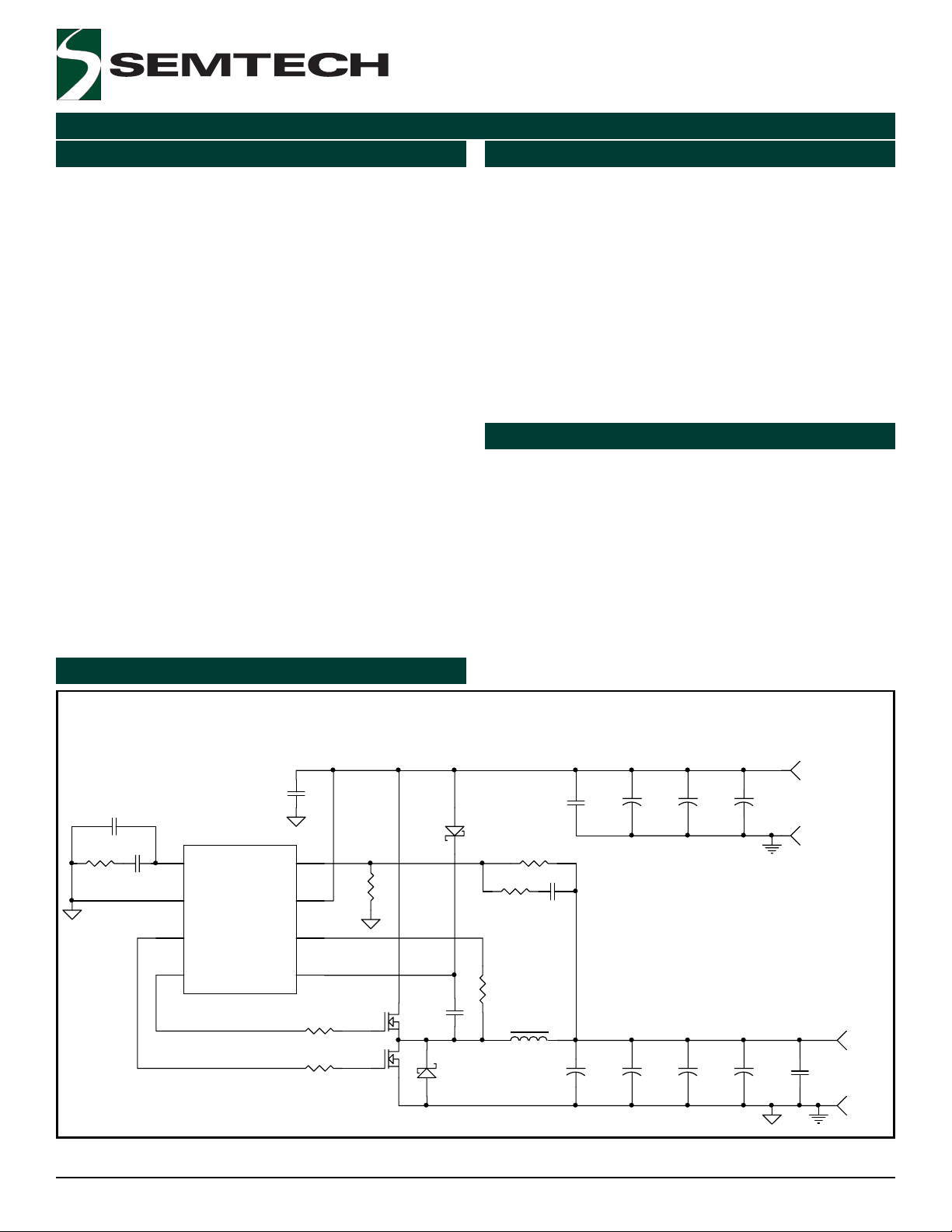
Typical Application Circuit
Typical Distributed Power Supply
C1
510-1500pF
U1
COMP /SS
GND
DL
DH
SC1104A/B
SENSE
VCC
PHASE
BST
R1
200-2k
C2
0.01
1
2
3
4
C3
1
8
7
6
5
R6
1-5.1
R7
1-5.1
Q1
Si4884DY
Q2
Si4874DY
R3
1.00k
D1
MBRA130L
C9
0.1
(opt)
+
C4
10.0
R4
2.32k
R5
0.1-0.33
L1
1.5-6.8uH
C8
C10
220/4V
200-1k
R8
opt
D2
C5
47/16V
C11
220/4V
C6
47/16V
C12
220/4V
C7
47/16V
C13
220/4V
Vin 5 to 12V
_
+
C14-17
3.3V
1.0
_
Revision: November 22, 2006
Figure 1
1
www.semtech.com
Page 2
SC1104A/B
POWER MANAGEMENT
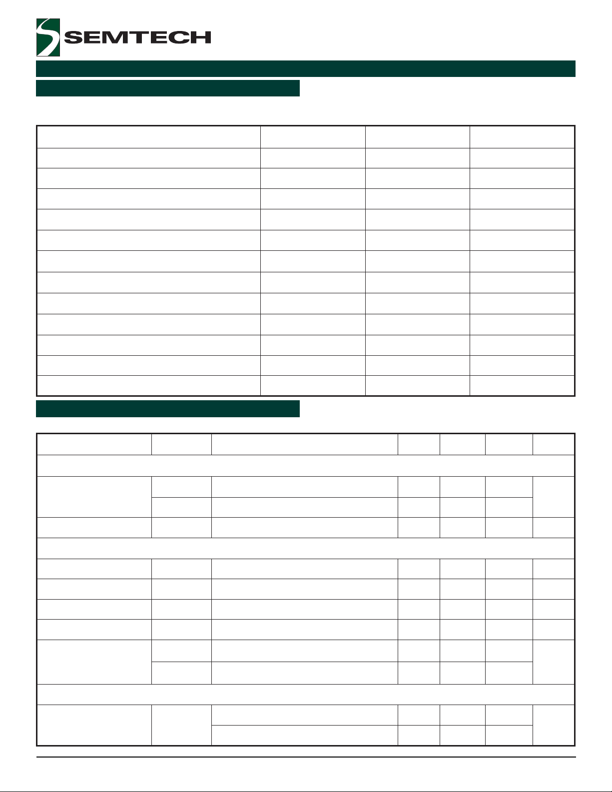
Absolute Maximum Ratings
Exceeding the specifications below may result in permanent damage to the device, or device malfunction. Operation outside of the parameters specified
in the Electrical Characteristics section is not implied. Exposure to Absolute Maximum rated conditions for extended periods of time may affect device
reliability.
retemaraPlobmySmumixaMstinU
V
CC
DNGot 02+V
ESAHPotTSB 02+V
DNGotESAHP 02+ot5.0-V
DNGotSS/PMOC 7+V
DNGotESNES 7+V
egnaRerutarepmeTegarotST
Electrical Characteristics
Unless specified: A: VCC = 12 ± 0.6V, V
retemaraPlobmySsnoitidnoCniMpyTxaMstinU
esaCotnoitcnuJecnatsiseRlamrehT
tneibmAotnoitcnuJecnatsiseRlamrehT
egnaRerutarepmeTnoitcnuJgnitarepOT
egnaRerutarepmeTtneibmAgnitarepOT
.ceS01)gniredloS(erutarepmeTdaeLT
)ledoMydoBnamuH(gnitaRDSEV
= 23 ± 1V, V
BST
= 3.3V, TJ = TA = 25oC.
OUT
θ
CJ
θ
AJ
J
A
GTS
daeL
DSE
B: V
= 5 ± 0.25V, V
CC
04W/C°
061W/C°
521+ot04-C°
58+ot04-C°
051+ot56-C°
003C°
2Vk
= 12 ± 0.6V, V
BST
= 2.0V, TJ = TA = 25oC
OUT
ylppuSrewoP
egatloVylppuSV
tnerruCylppuSI
CC
V
CC
CC
F
WS
F
WS
reifilpmArorrE
)1(
ecnatcudnocsnarTA/E
)1(
niaGCDpooLnepO
)1(
Bd3-htdiwdnaB
tnerruCsaiBtupnII
tnerruCkniStuptuO
tnerruCecruoS
g
m
A
O
F
WB
BF
I
KIS
I
CS
V
V
rotallicsO
ycneuqerFgnihctiwSF
CSO
A4011CS,).mon(zHk003=5.441V
B4011CS,).mon(zHk006=5.47
V
≤ V4.01141Am
PMOC
21Sm
24Bd
004zHk
13 Aµ
≥ V;V1.1
ESNES
V5.1=56.07.0
PMOC
Am
≥ V;V9.0
ESNES
V
CC
V5.1=59.01.1
PMOC
V6.0±V21=552003543
zHk
V
CC
V52.0±V5=015006096
© 2006 Semtech Corp.
2
www.semtech.com
Page 3
POWER MANAGEMENT
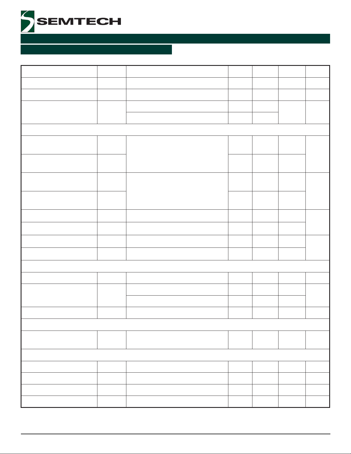
Electrical Characteristics
Unless specified: A: VCC = 12 ± 0.6V, V
retemaraPlobmySsnoitidnoCniMpyTxaMstinU
)1(
egatloVkaePpmaR
)1(
egatloVyellaVpmaR
)2(
elcyCytuDmumixaM
srevirDTEFSOM
= 23 ± 1V, V
BST
V
K-P
V
V
cd
SC1104A/B
= 3.3V, TJ = TA = 25oC.
OUT
V57.4 ≤ VCC≤ V6.210.2V
V57.4 ≤ VCC≤ V6.210.1V
XAM
V
CC
V
CC
B: VCC = 5 ± 0.25V, V
)A4011CS,zHk003(V21=0959%
)B4011CS,zHk006(V5=5809
= 12 ± 0.6V, V
BST
= 2.0V, TJ = TA = 25oC
OUT
tnerruCecruoS/kniSHD
A4011CS
tnerruCecruoS/kniSLD
A4011CS
tnerruCecruoS/kniSHD
B4011CS
tnerruCecruoS/kniSLD
B4011CS
emiTllaF/esiRHDft,rtC
emiTllaF/esiRLDft,rtC
emiTdaeDt
emiTffOmuminiMHDt
I
HD
V
I
LD
I
HD
V
V
I
LD
td
FFO
V
L
L
t,%2<.c.d
WP
SG
SG
t,%2<.c.d
WP
SG
SG
V57.4 ≤ ccV ≤ V6.21061
noitceSecnerefeR
egatloVecnerefeRV
ecnairaVpmeT
∆V
FER
FER
ytilibatSmreTgnoLT
V57.4 ≤ ccV ≤ V6.21099.0000.1010.1V
T<0
J
T<04-
J
J
timiLtnerruC
sµ001<
6.08.0A
)crs(V5.4=
)kns(V5.2=
sµ001<
6.07.0
54.06.0A
)crs(V5.4=
)kns(V5.2=
54.06.0
2.giFeeS,Fp0003=05sn
2.giFeeS,Fp0004=05
2.giFeeS08sn
C°07+<1-1%
C°58+<5.1-5.1
.srh0001,C°521=5Vm
egatloVpirTV
elbanE/tratS-tfoS
tnerruCecruoSSSI
tnerruCkniSSSI
© 2006 Semtech Corp.
PIRT
CRS
KNS
V57.4<ccV< V6.21
V
prt
V
PMOC
V
PMOC
V-ccV=
ESAHP
V5.2<5.08.1Aµ
V5.0>5.08.1Aµ
081002022Vm
dlohserhTtupnIelbanE 00.153.1V
tnerruCtupnIelbanEV
V8.0=2Am
PMOC
3
www.semtech.com
Page 4
POWER MANAGEMENT
Electrical Characteristics
Unless specified: A: VCC = 12 ± 0.6V, V
retemaraPlobmySsnoitidnoCniMpyTxaMstinU
tuokcoLegatloVrednU
= 23 ± 1V, V
BST
= 3.3V, TJ = TA = 25oC.
OUT
B: V
CC
= 5 ± 0.25V, V
= 12 ± 0.6V, V
BST
SC1104A/B
= 2.0V, TJ = TA = 25oC
OUT
dlohserhTOLVUV
nwodtuhSlamrehT
)2(
tnioPpirTerutarepmeTrevO
Notes:
(1) Guaranteed by design.
(2) Not tested, by characterization.
ht
T
PTO
T<04-
C°58<9.351.45.4V
J
041061C°
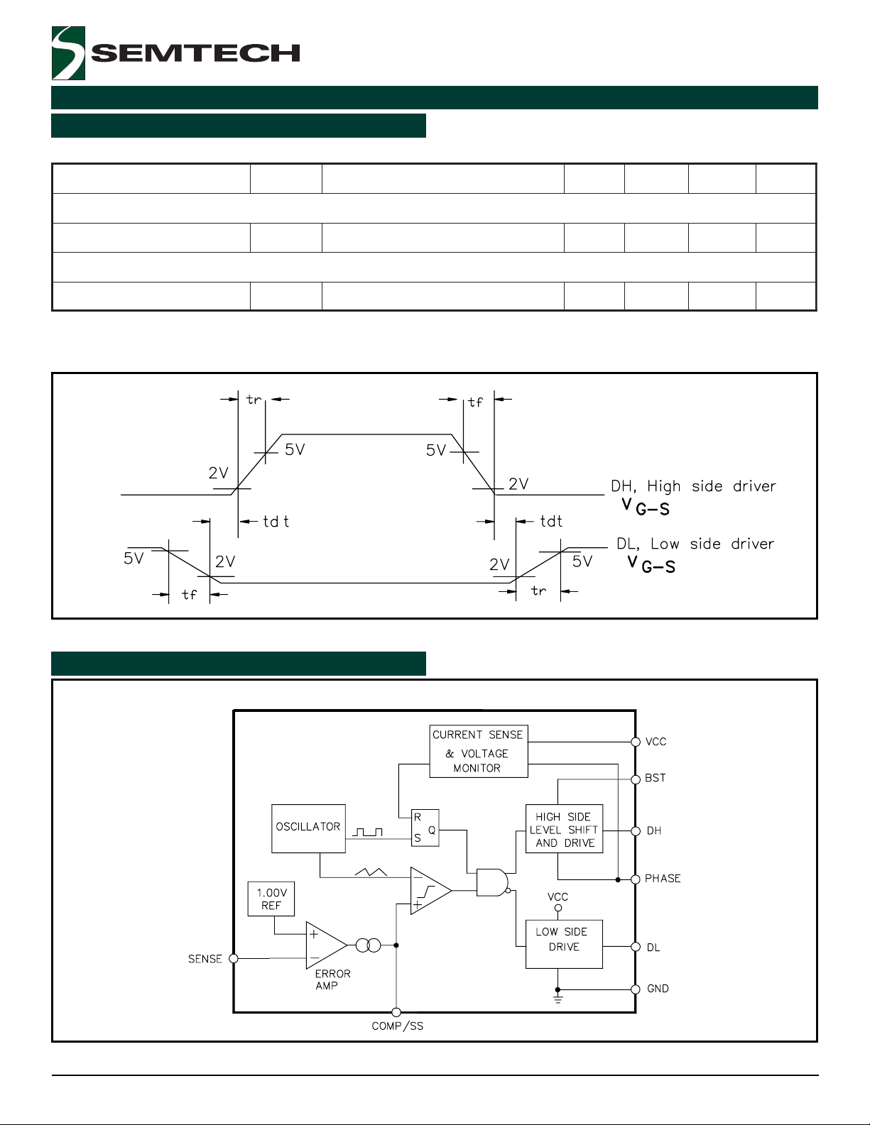
Figure 2
Block Diagram
Figure 3
© 2006 Semtech Corp.
4
www.semtech.com
Page 5
POWER MANAGEMENT
SC1104A/B
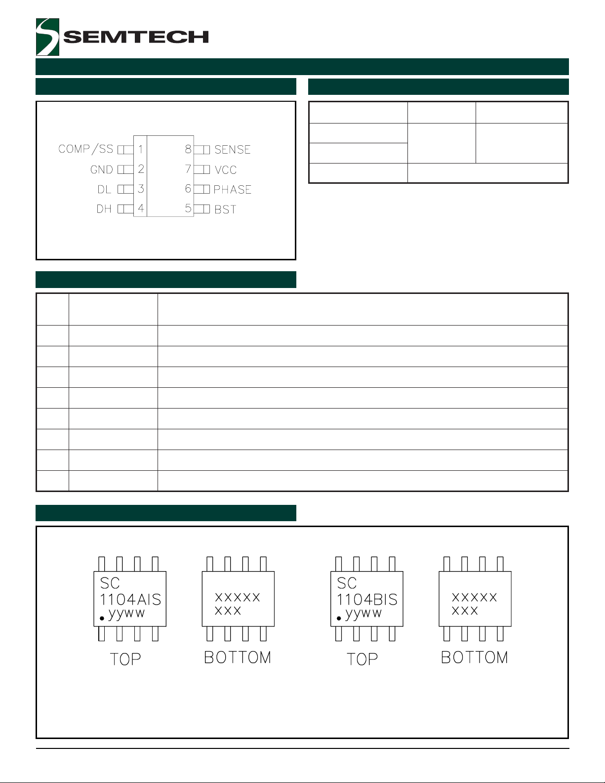
Pin Configuration
(8-Pin SOI
Pin Descriptions
niP
#
1SS/PMOC.elbane/tratstfos,noitasnepmoC.tuptuoreifilpmarorrE
2DNG.dnuorG
emaNniPnoitcnuFniP
Top View
C)
Ordering Information
)2(
eciveD
)1(
RTSIX4011CS
)3()1(
TRTSIX4011CS
BVEX4011CSdraoBnoitaulavE
Notes:
(1) In place of “X”: A = 300kHz, V
B = 600kHz, V
(2) Only available in tape and reel packaging. A reel
contains 2500 devices.
(3) Lead free product. This product is fully WEEE and
RoHS compliant.
egakcaPT(egnaRpmeT
8-CIOSC°521ot°04-
= 5V to 12V.
CC
= 5V.
CC
)
J
3LDtuptuorevirdediswoL
4HDtuptuorevirdedishgiH
5TSB.revirdedishgih,partstooB
6ESAHP.sTEFSOMehtneewtebedonesahpehtmorftupnI
7CCV.egatlovylppussaibpihC
8ESNES.tupniesnesegatlovtuptuO
Marking Information
© 2006 Semtech Corp.
yyww = Date Code (Example: 0012)
xxxxxxxx = Semtech Lot No. (Example: E90101-1)
5
www.semtech.com
Page 6

POWER MANAGEMENT
Theory of Operation
Synchronous Buck Converter
SC1104A/B
The output voltage of the synchronous converter is set
and controlled by the output of the error amplifier. The
inverting input of the error amplifier receives its voltage
from the SENSE pin. The non-inverting input of the error
amplifier is connected to an internal 1V reference.
The error amplifier output is connected to the
COMPensation pin. The error amplifier generates a current proportional to (Vsense – 1V), which is the COMP
pin output current (Transconductance ~ 12mS). The
voltage on the COMP pin is the integral of the error amplifier current. The COMP voltage is the non-inverting
input to the PWM comparator and controls the duty cycle
of the MOSFET drivers. The size of capacitor Ccomp controls the stability and transient response of the regulator. The larger the capacitor, the slower the COMP voltage changes, and the slower the duty cycle changes.
The inverting input voltage of the PWM comparator is
the triangular output of the oscillator.
When the oscillator output voltage drops below the COMP
voltage, the comparator output goes high. This pulls DL
low, turning off the low-side FET. After a short delay (“dead
time”), DH is pulled high, turning on the high-side FET.
When the oscillator voltage rises back above the error
amplifier output voltage, the comparator output goes low.
This pulls DH low, turning off the high-side FET, and after
a dead time delay, DL is pulled high, turning on the lowside FET. The dead time delay is determined by a
monostable on the chip.
The triangle wave minimum is about 1V, and the maximum is about 2V. Thus, if Vcomp = 0.9V, high side duty
cycle is the minimum (~0%) , but if Vcomp is 2.0V, duty
cycle is at maximum ( ~90%).The internal oscillator uses
an on-chip capacitor and trimmed precision current
sources to set the oscillation frequency to 300kHz
(SC1104A) or 600kHz (SC1104B).
Figure 1 shows a 3.3V output converter. If the Vout <3.3V,
then the SENSE voltage < 1V. In this case the error
amplifier will be sourcing current into the COMP pin so
that COMP voltage and duty cycle will gradually increase.
If Vout > 3.3V, the error amplifier will sink current and
reduce the COMP voltage, so that duty cycle will decrease.
The circuit will be in steady state when Vout =3.3V ,
Vsense = 1V, Icomp = 0 . The COMP voltage and duty
cycle depend on Vin.
Under Voltage Lockout
The under voltage lockout circuit of the SC1104A/B assures that both high-side and low-side MOSFET driver
outputs remain in the off state whenever the supply voltage drops below set parameters. Lockout occurs if V
falls below 4.2V typ.
R
Current Limiting
DS(ON)
In case of a short circuit or overload, the high-side (HS)
FET will conduct large currents. To prevent damage, in
this situation, large currents will generate a fault condition and begin a soft start cycle.
While the HS driver is on, the phase voltage is compared
to the Vcc pin voltage. If the phase voltage is 200mV
lower than Vcc, a fault is latched and the soft start cycle
begins.
The voltages are compared during the middle of the HS
pulse, to prevent transients from affecting the accuracy.
The sampling of the voltage across the top FET occurs
after a time delay t
= 100ns_typ from the time the
DELAY
DH is pulled high. This delay prevents the measurement
to be effected by ringing on the leading edge of the phase
node pulse. The duration of the sampling is t
SAMPLE
=
100ns_typ. It is being disabled at very low duty cycle when
tON < 300ns_typ. This feature allows for the orderly startup during the inrush of the current charging output capacitor and the fault free operation with extremely high
input/output voltage ratio, e.g., VIN = 12V and V
OUT
= 1V.
The over-current comparator (OC) is only active if the
phase node is > 3.3V. This means that in the case of
power source being < 3V the OC will be disabled even
though the rest of the circuitry is completely functional.
SC1104 still can be used for stepping down, e.g. 2.8V to
2.5V, 2V, 1.8V, etc.
CC
© 2006 Semtech Corp.
6
www.semtech.com
Page 7
POWER MANAGEMENT
Theory of Operation (Cont.)
SC1104A/B
When choosing OC trip point one should consider the
Tempco of the MOSFETs Rds_on and SC1104’s Vtrip.
Also, any ringing on the Vcc and Phase nodes due to
parasitic L and C will have some effect on the OC Vtrip.
Example:
Iout_nom = 6A; assume I_max = 125% • Iout_nom =
7.5A
Rds_on = 0.014Ω; assume Rds_on_max
≈ 150% •
Rds_on = 0.02Ω
Voc = 7.5A • 0.02Ω = 150mV.
This proves that MOSFETs with R
= 0.014Ω @ 25°C
DS_ON
is the right choice.
Soft Start
The soft start (or hiccup) circuitry is activated when a
fault occurs. Faults occur for three reasons:
Closing the Loop
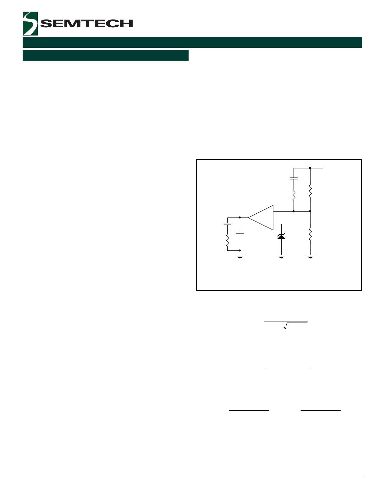
In order to have a stable closed loop system with optimum
transient response one should make sure that open-loop
frequency response has an adequate Gain & Phase
margins. The Bode plot of log. Gain vs Freq. and Phase
vs Freq. provide the necessary means for the circuit
evaluation. Loop stability defined by compensation
networks around transconductance error amplifier (EA)
and output divider, see below and output capacitor Cout
and inductor Lout.
Vout
Cn
Rn
EA
_
C
C
R
C
Gm
+
Cp
Vref
Ra
Rb
1) Under voltage (VCC < 4.2V)
2) Over temperature (die temperature > 150°C)
3) Over current in high side FET.
All faults are handled the same way. Both DH and DL are
forced low. The error amplifier is turned off, but a 2µA
current flows into the comp pin (soft start current). The
sink current reduces the Comp voltage down to 0.6V
over a period of a few milliseconds. When Vcomp ~ 0.6V,
the fault is cleared and the DL goes high. Also, the soft
start current changes polarity and begins to increase the
voltage on the Comp capacitor. The DH remains low, because Vcomp is less than the lowest excursion of the
oscillator ramp (1.0V). After a few ms, the Vcomp increases to about 1.0V and the DH will start to switch.
The duty cycle will gradually increase, and Vsns will increase. When Vsns ~ 1.00V, the error amplifier turns on
again. The circuit has now reached its operating point. If
a fault occurs during the soft start, the cycle will begin
again (drivers low, Vcomp decreasing down to 0.6V).
Typical transconductance error amplifier
The inductor and output capacitor form a “double pole”
at the frequency:
∏
1
•••
CoLo2
=
f
LC
The ESR of the output capacitor and the output capacitor
value create a “zero” at the frequency.
f
ESR
=
∏
1
•••
CoESR2
The “zero” and “pole” from the EA compensation network
are:
∏
1
•••
CcRc2
=
f
P
=
f
Z
∏
1
•••
CpRc2
The additional “lead” network RA, CN, RN can be used to
improve phase margin in case when output capacitors
with extra-low ESR are used and there is a need to
compensate for “high quality” output Lo, Co filter.
© 2006 Semtech Corp.
7
www.semtech.com
Page 8
POWER MANAGEMENT
Theory of Operation (Cont.)
SC1104A/B
f
NET
=
∏
1
•••
CnRa2
Value for the resistor RN should be 1/10 of the output
divider upper resistor RA.
Example.
Switching frequency fSW = 300kHz
Output capacitance C
Output capacitor ESR = 45mΩ/each
Output inductance L
= 3 x 330µF
OUT
= 4.7µH
OUT
Input voltage VIN = 12V
Output voltage V
= 3.3V
OUT
Let’s choose crossover frequency
f
= 1/20 • f
CO
= 15kHz
SW
The compensation values used in this example are based
on the following criteria:
f
= fLC; f
Z
= 1/10 • f
NET
; f
LC
= 10 • f
P
= 150kHz
CO
attenuation due to the LO, CO filter and the output
resistor divider R
, RB is compensated by the gain of
A
the PWM modulator and the gain of the
transconductance error amplifier (Gm
• Z
EA
COMP
).
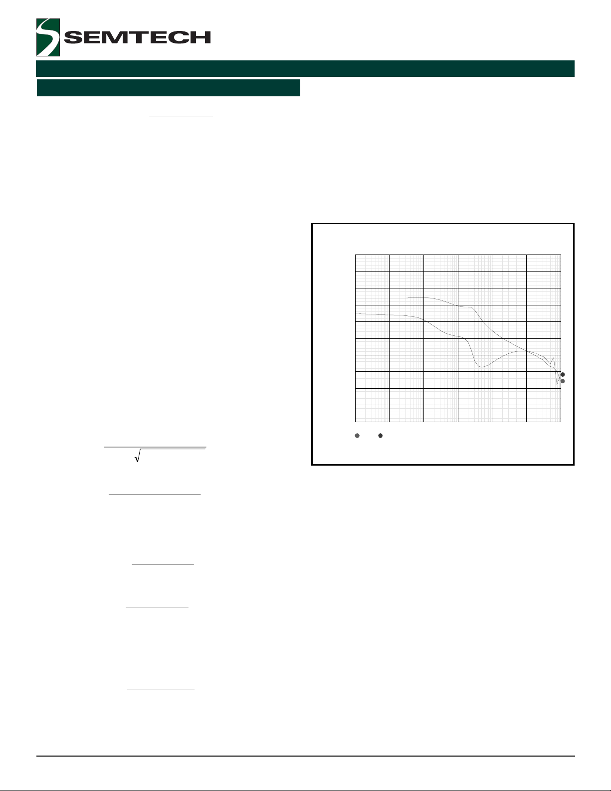
Shown below is a typical Bode plot of the open-loop
frequency response of SC1104 based buck converter.
80.0
-50.0
40.0
-150
0
-250
Plot1
vpherr in degrees
vdberr in db(volts)
-40.0
-80.0
-350
-450
2
1
Therefore,
f
LC
f
ESR
=
1
∏
=
1
∏
=
µ•••
F990H4.7µ2
=
F990015.02
µ•••
kHz33.2
kHz72.10
Since, the EA can sink/source about 1mA, let’s choose
Rc = 680Ω, then
∏
∏
1
•••
RcFz2
1
=
RcFp2
•••
F1.0
pF1500
C µ=
=
C
C
=
P
Assuming the output divider lower resistor RB = 1k, then
for V
= 3.3V the RA = 2.32k.
OUT
=
C
N
∏
1
NET
µ=
•••
Raf2
F3.0
At the closed-loop crossover frequency fCO, the
1 10 100 1k 10k 100k 1Meg
1 vdberr 2 vpherr
frequency in hertz
© 2006 Semtech Corp.
8
www.semtech.com
Page 9
POWER MANAGEMENT
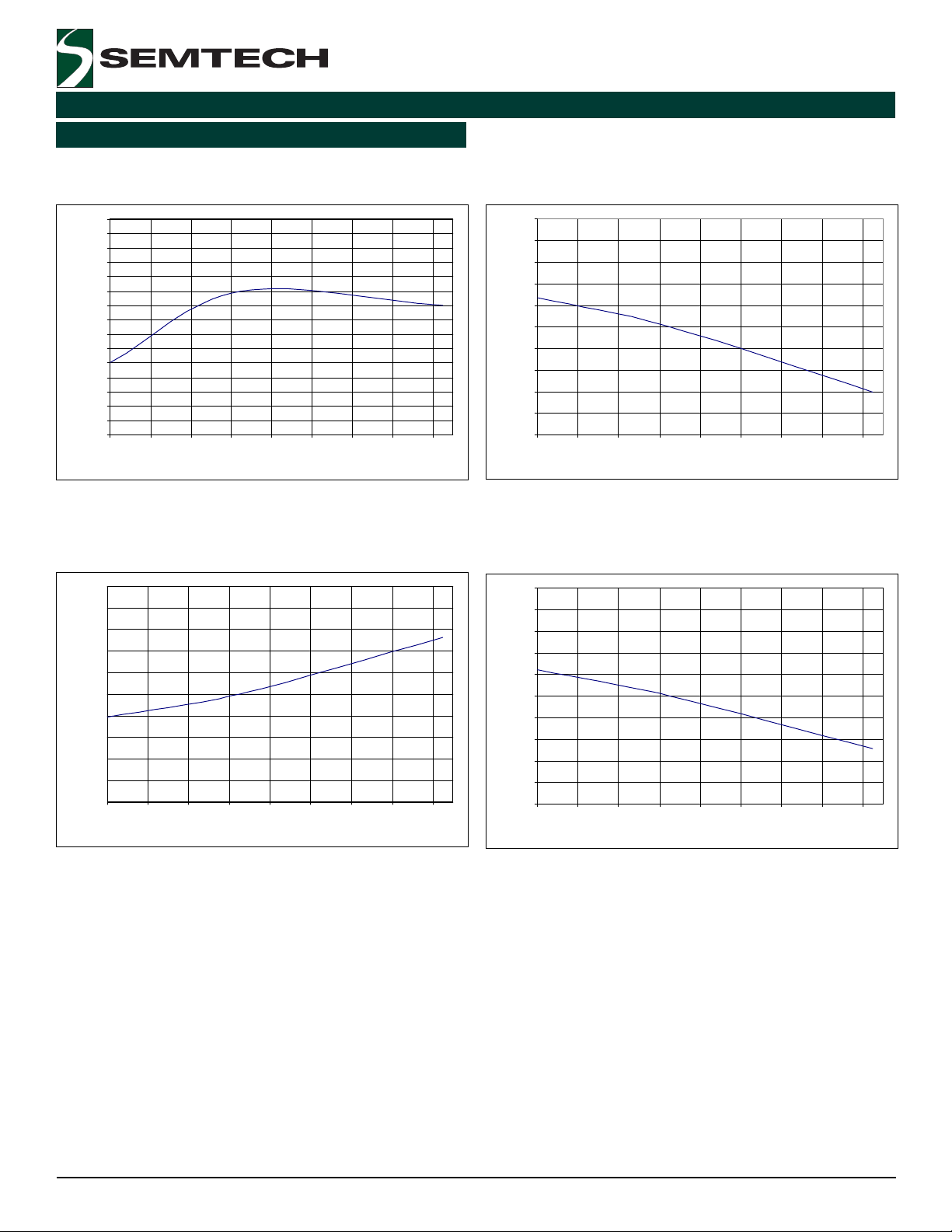
Typical Characteristics
SC1104A/B
Reference Voltage vs. Temp
0.5%
0.4%
0.3%
0.2%
0.1%
0.0%
-0.1 %
-0.2 %
-0.3 %
Vref, %
-0.4 %
-0.5 %
-0.6 %
-0.7 %
-0.8 %
-0.9 %
-1.0 %
-40-20020406080100120
Temp, °C
Trip Voltage vs. Temp
25%
20%
15%
10%
5%
0%
Vtrip, %
-5%
-10%
-15%
-20%
-25%
-40-20 0 20406080100120
Temp, °C
Switching Frequency vs. Temp
25%
20%
15%
10%
5%
0%
Freq, %
-5%
-10%
-15%
-20%
-25%
-40-200 20406080100120
Temp, °C
Under Voltage Lockout vs. Temp
10%
8%
6%
4%
2%
0%
UVLO, %
-2%
-4%
-6%
-8%
-10%
-40-200 20406080100120
Temp, °C
© 2006 Semtech Corp.
9
www.semtech.com
Page 10
POWER MANAGEMENT
0
0
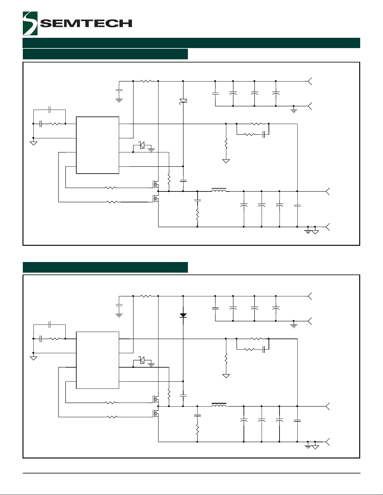
Evaluation Board Schematic - V
C3
1.0
C1
C2
0.1
1500p
R1
1k
1
2
3
SC11 04A ISTR
COMP/SS
GND
DL
U1
8
SENSE
7
VCC
PHASE
MBRA13 0L(o pt)
6
D2
= 5V
IN
D1
MBRA13 0L
C7
10.0
R7
1.0k
C8
47/6.3V
R9
150
R8
1.50k
C9
47/6.3V
C11
0.47
SC1104A/B
+
C10
47/6.3V
Vin=5V
_
4
DH
R3
1
R4
2.2
BST
5
Q1
Si44 10DY
Q2
Si44 10DY
Evaluation Board Schematic - VIN = 12V
C3
1.0
C1
C2
0.1
1500p
R1
680
1
2
3
SC11 04A ISTR
COMP/SS
GND
DL
U1
8
SENSE
D2
7
VCC
PHASE
MBRA13 0L(o pt)
6
R5
0
C4
0.1
D1
LL4148
C5
6800p
R6
2.2
C7
10.0
L1
3.9uH
R7
1.0k
C8
33/16V
C15
330/4V
R8
2.32k
R9
220
C16
330/4V
C9
33/16V
C11
0.33
C17
330/4V
C10
33/16V
C18
10
+
Vout=2.5@6A
_
+
Vin=12V
_
4
DH
© 2006 Semtech Corp.
R3
2.2
R4
2.2
BST
5
Q1
Si44 10DY
Q2
Si44 10DY
R5
5.1opt
C4
0.1
10
C5
3300p
R6
3.3
L1
4.7uH
C15
330/4V
C16
330/4V
C17
330/4V
C18
10
Vout=3.3@6A
www.semtech.com
+
_
Page 11
POWER MANAGEMENT
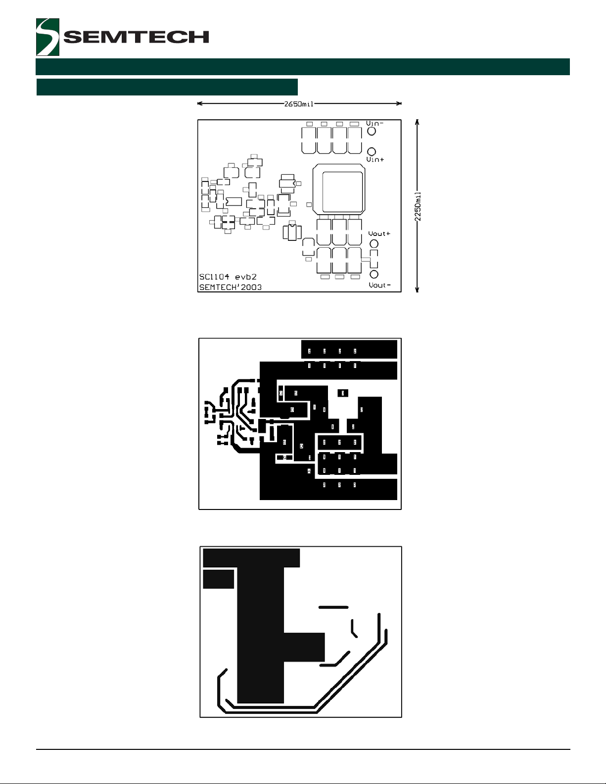
Evaluation PC Board
SC1104A/B
Top View
© 2006 Semtech Corp.
Top Layer
Bottom Layer
11
www.semtech.com
Page 12
POWER MANAGEMENT
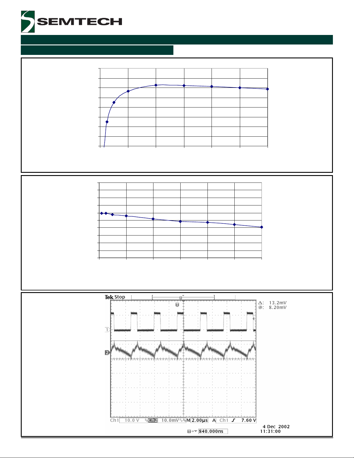
Typical Characteristics
100%
95%
90%
SC1104A/B
Efficiency
1.0%
0.8%
0.6%
0.4%
0.2%
0.0%
-0.2%
-0.4%
Regulation
-0.6%
-0.8%
-1.0%
85%
80%
75%
70%
65%
60%
024681012
Current, A
024681012
12V = Vin
3.3V = Vout
12A = Iout
© 2006 Semtech Corp.
Current, A
12
www.semtech.com
Page 13
POWER MANAGEMENT
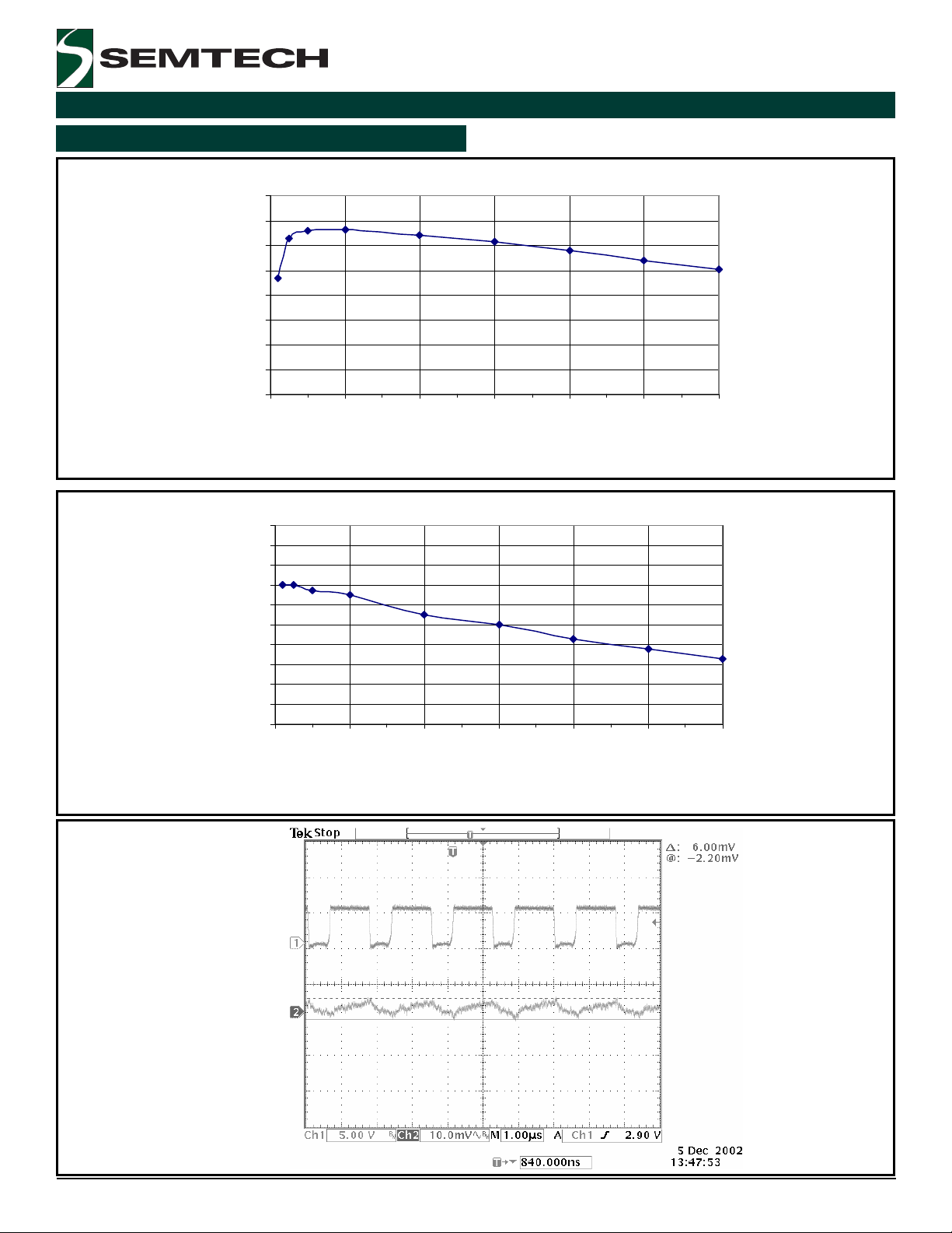
Typical Characteristics (Cont.)
100%
95%
90%
85%
80%
75%
Efficiency
70%
65%
60%
024681012
SC1104A/B
5V = Vin
2V = Vout
12A = Iout
Current, A
-0.2%
Regula tion
-0.4%
-0.6%
-0.8%
-1.0%
1.0%
0.8%
0.6%
0.4%
0.2%
0.0%
024681012
Current, A
© 2006 Semtech Corp.
13
www.semtech.com
Page 14
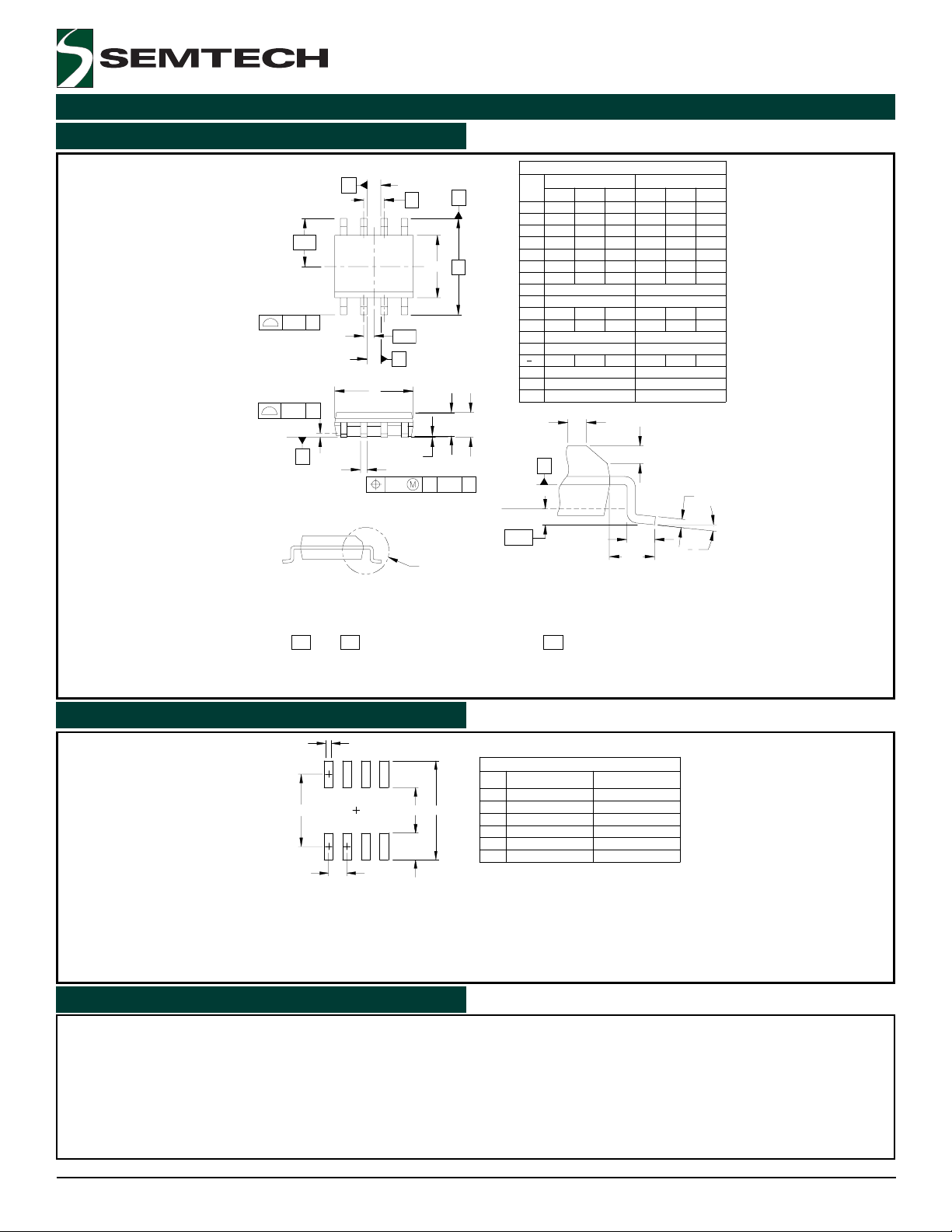
POWER MANAGEMENT
,
Outline Drawing - SOIC - 8
SC1104A/B
A
N
E/2
2X
12
ccc C
2X N/2 TIPS
aaa C
SEATING
PLANE
NOTES:
CONTROLLING DIMENSIONS ARE IN MILLIMETERS (ANGLES IN DEGREES).
1.
DATUMS AND TO BE DETERMINED AT DATUM PLANE
2.
3. DIMENSIONS "E1" AND "D" DO NOT INCLUDE MOLD FLASH, PROTRUSIONS
OR GATE BURRS.
REFERENCE JEDEC STD MS-012, VARIATION AA.
4.
C
SIDE VIEW
-A- -H-
-B-
e/2
B
D
bxN
bbb C A-B D
e
E1
A2
A1
SEE DETAIL
D
E
A
PLANE
A
DIM
GAGE
0.25
A1
A2
D
E1
L1
N
01
aaa
bbb
ccc
A
b
c
E
e
h
L
H
DIMENSIONS
INCHES
NOM
MIN MAX MAXNOM
-
.053
-
.004
-
.049
-
.012
-
.007
.189
.193
.150
.154
.236 BSC
.050 BSC
-
.010 .020 0.50
.028
.016
(.041)
8
-
0°
.004
.010
.008
h
DETAIL
MILLIMETERS
MIN
.069
1.35
0.10
.010
1.25
.065
.020 0.31
.010
0.17
.197
4.80
.157
3.80
0.25
.041
0.40
8° 0°
h
L
(L1)
A
-
-
-
-
4.90
3.90
6.00 BSC
1.27 BSC
-
0.72-1.04
(1.04)
8
-
0.10
0.25
0.20
01
c
1.75
0.25
1.65
0.51
0.25
5.00
4.00
8°
Minimum Land Pattern - SOIC - 8
X
(C)
P
NOTES:
1.
THIS LAND PATTERN IS FOR REFERENCE PURPOSES ONLY.
CONSULT YOUR MANUFACTURING GROUP TO ENSURE YOUR
COMPANY'S MANUFACTURING GUIDELINES ARE MET.
2.
REFERENCE IPC-SM-782A
Contact Information
Power Management Products Division
200 Flynn Road, Camarillo, CA 93012
Phone: (805)498-2111 FAX (805)498-3804
INCHES
G
Z
Y
RLP NO. 300A.
DIM
C
G
P
X
Y
Z
(.205) (5.20)
.118
.050
Semtech Corporation
DIMENSIONS
MILLIMETERS
3.00
1.27
0.60.024
2.20.087
7.40.291
© 2006 Semtech Corp.
14
www.semtech.com
 Loading...