

Page 1
December 1994 Order Number: 290479-004
82434LX/82434NX PCI, CACHE AND MEMORY
CONTROLLER (PCMC)
Y
Supports the PentiumTMProcessor at
iCOMP
TM
Index 510T60 MHz and iCOMP
Index 567T66 MHz
Y
Supports the Pentium Processor at
iCOMP Index 735T90 MHz, iCOMP Index
815T100 MHz, and iCOMP Index 610T75
MHz
Y
Supports Pipelined Addressing
Capability of the Pentium Processor
Y
The 82430NX Drives 3.3V Signal Levels
on the CPU and Cache Interfaces
Y
High Performance CPU/PCI/Memory
Interfaces via Posted Write and Read
Prefetch Buffers
Y
Fully Synchronous PCI Interface with
Full Bus Master Capability
Y
Supports the Pentium Processor
Internal Cache in Either Write-Through
or Write-Back Mode
Y
Programmable Attribute Map of DOS
and BIOS Regions for System
Flexibility
Y
Integrated Low Skew Clock Driver for
Distributing Host Clock
Y
Integrated Second Level Cache
Controller
Ð Integrated Cache Tag RAM
Ð Write-Through and Write-Back Cache
Modes for the 82434LX
Ð Write-Back for the 82434NX
Ð 82434NX Supports Low-Power Cache
Standby
Ð Direct Mapped Organization
Ð Supports Standard and Burst SRAMs
Ð 256-KByte and 512-KByte Sizes
Ð Cache Hit Cycle of 3-1-1-1 on Reads
and Writes Using Burst SRAMs
Ð Cache Hit Cycle of 3-2-2-2 on Reads
and 4-2-2-2 on Writes Using
Standard SRAMs
Y
Integrated DRAM Controller
Ð Supports 2 MBytes to 192 MBytes of
Cacheable Main Memory for the
82434LX
Ð Supports 2 MBytes to 512 MBytes of
Cacheable Main Memory for the
82434NX
Ð Supports DRAM Access Times of
70 ns and 60 ns
Ð CPU Writes Posted to DRAM 4-1-1-1
Ð Refresh Cycles Decoupled from ISA
Refresh to Reduce the DRAM
Access Latency
Ð Six RAS
Ý
Lines (82434LX)
Ð Eight RAS
Ý
Lines (82434NX)
Ð Refresh by RAS
Ý
-Only, or CAS-
Before-RAS
Ý
, in Single or Burst
of Four
Y
Host/PCI Bridge
Ð Translates CPU Cycles into PCI Bus
Cycles
Ð Translates Back-to-Back Sequential
CPU Memory Writes into PCI Burst
Cycles
Ð Burst Mode Writes to PCI in Zero PCI
Wait-States (i.e. Data Transfer Every
Cycle)
Ð Full Concurrency Between CPU-to-
Main Memory and PCI-to-PCI
Transactions
Ð Full Concurrency Between CPU-to-
Second Level Cache and PCI-to-Main
Memory Transactions
Ð Same Cache and Memory System
Logic Design for ISA and EISA
Systems
Ð Cache Snoop Filter Ensures Data
Consistency for PCI-to-Main Memory
Transactions
Y
208-Pin QFP Package
*Other brands and names are the property of their respective owners.
Page 2

82434LX/82434NX
This document describes both the 82434LX and 82434NX. Unshaded areas describe the 82434LX.
Shaded areas, like this one, describe 82434NX operations that differ from the 82434LX.
The 82434LX/82434NX PCI, Cache, Memory Controllers (PCMC) integrate the cache and main memory
DRAM control functions and provide bus control for transfers between the CPU, cache, main memory, and the
PCI Local Bus. The cache controller supports write-back (or write-through for 82434LX) cache policy and
cache sizes of 256-KBytes and 512-KBytes. The cache memory can be implemented with either standard or
burst SRAMs. The PCMC cache controller integrates a high-performance Tag RAM to reduce system cost.
2
Page 3
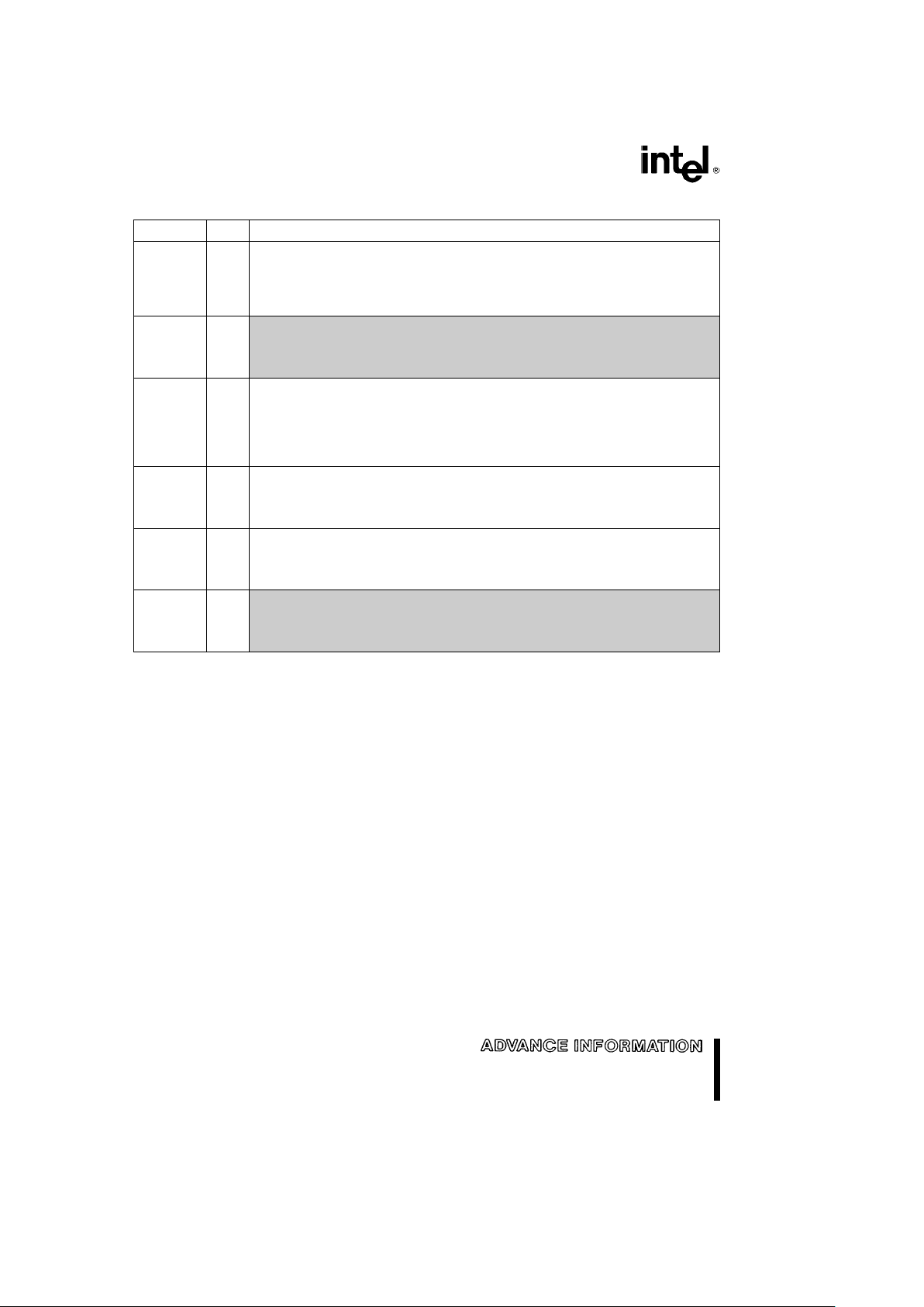
82434LX/82434NX
290479– 1
NOTE:
RAS[7:6
]
Ý
and MA11 are only on the 82434NX. CCS[1:0]functionality is only on the 82434NX.
Simplified Block Diagram of the PCMC
3
Page 4

82434LX/82434NX PCI, CACHE AND MEMORY
CONTROLLER (PCMC)
CONTENTS PAGE
1.0 ARCHITECTURAL OVERVIEW
АААААААААААААААААААААААААААААААААААААААААААААААААААААААААА 10
1.1 System Overview АААААААААААААААААААААААААААААААААААААААААААААААААААААААААААААААААААААА 10
1.1.1 BUS HIERARCHYÐCONCURRENT OPERATIONS ААААААААААААААААААААААААААААААА 10
1.1.2 BUS BRIDGES ААААААААААААААААААААААААААААААААААААААААААААААААААААААААААААААААААА 13
1.2 PCMC Overview ААААААААААААААААААААААААААААААААААААААААААААААААААААААААААААААААААААААА 13
1.2.1 CACHE OPERATIONS ААААААААААААААААААААААААААААААААААААААААААААААААААААААААААА 14
1.2.1.1 Cache Consistency АААААААААААААААААААААААААААААААААААААААААААААААААААААААААА 15
1.2.2 ADDRESS/DATA PATHS АААААААААААААААААААААААААААААААААААААААААААААААААААААААА 15
1.2.2.1 Read/Write Buffers АААААААААААААААААААААААААААААААААААААААААААААААААААААААААА 15
1.2.3 HOST/PCI BRIDGE OPERATIONS ААААААААААААААААААААААААААААААААААААААААААААААА 15
1.2.4 DRAM MEMORY OPERATIONS АААААААААААААААААААААААААААААААААААААААААААААААААА 16
1.2.5 3.3V SIGNALS ААААААААААААААААААААААААААААААААААААААААААААААААААААААААААААААААААА 16
2.0 SIGNAL DESCRIPTIONS АААААААААААААААААААААААААААААААААААААААААААААААААААААААААААААААА 16
2.1 Host Interface ААААААААААААААААААААААААААААААААААААААААААААААААААААААААААААААААААААААААА 17
2.2 DRAM Interface ААААААААААААААААААААААААААААААААААААААААААААААААААААААААААААААААААААААА 22
2.3 Cache Interface ААААААААААААААААААААААААААААААААААААААААААААААААААААААААААААААААААААААА 23
2.4 PCI Interface АААААААААААААААААААААААААААААААААААААААААААААААААААААААААААААААААААААААААА 24
2.5 LBX Interface ААААААААААААААААААААААААААААААААААААААААААААААААААААААААААААААААААААААААА 28
2.6 Reset And Clock АААААААААААААААААААААААААААААААААААААААААААААААААААААААААААААААААААААА 28
3.0 REGISTER DESCRIPTION ААААААААААААААААААААААААААААААААААААААААААААААААААААААААААААААА 30
3.1 I/O Mapped Registers ААААААААААААААААААААААААААААААААААААААААААААААААААААААААААААААААА 31
3.1.1 CONFADDÐCONFIGURATION ADDRESS REGISTER ААААААААААААААААААААААААААА 31
3.1.2 CSEÐCONFIGURATION SPACE ENABLE REGISTER ААААААААААААААААААААААААААА 32
3.1.3 TRCÐTURBO-RESET CONTROL REGISTER АААААААААААААААААААААААААААААААААААА 33
3.1.4 FORWÐFORWARD REGISTER АААААААААААААААААААААААААААААААААААААААААААААААААА 34
3.1.5 PMCÐPCI MECHANISM CONTROL REGISTER АААААААААААААААААААААААААААААААААА 34
3.1.6 CONFDATAÐCONFIGURATION DATA REGISTER ААААААААААААААААААААААААААААААА 34
3.2 PCI Configuration Space Mapped Registers АААААААААААААААААААААААААААААААААААААААААААА 35
3.2.1 CONFIGURATION SPACE ACCESS MECHANISM АААААААААААААААААААААААААААААААА 36
3.2.1.1 Access MechanismÝ1: АААААААААААААААААААААААААААААААААААААААААААААААААААААА 36
3.2.1.2 Access MechanismÝ2 АААААААААААААААААААААААААААААААААААААААААААААААААААААА 37
3.2.2 VIDÐVENDOR IDENTIFICATION REGISTER ААААААААААААААААААААААААААААААААААААА 40
3.2.3 DIDÐDEVICE IDENTIFICATION REGISTER АААААААААААААААААААААААААААААААААААААА 40
4
Page 5

CONTENTS PAGE
3.2.4 PCICMDÐPCI COMMAND REGISTER
ААААААААААААААААААААААААААААААААААААААААААА 41
3.2.5 PCISTSÐPCI STATUS REGISTER ААААААААААААААААААААААААААААААААААААААААААААААА 42
3.2.6 RIDÐREVISION IDENTIFICATION REGISTER ААААААААААААААААААААААААААААААААААА 43
3.2.7 RLPIÐREGISTER-LEVEL PROGRAMMING INTERFACE REGISTER ААААААААААААА 43
3.2.8 SUBCÐSUB-CLASS CODE REGISTER АААААААААААААААААААААААААААААААААААААААААА 43
3.2.9 BASECÐBASE CLASS CODE REGISTER АААААААААААААААААААААААААААААААААААААААА 44
3.2.10 MLTÐMASTER LATENCY TIMER REGISTER ААААААААААААААААААААААААААААААААААА 44
3.2.11 BISTÐBIST REGISTER ААААААААААААААААААААААААААААААААААААААААААААААААААААААААА 44
3.2.12 HCSÐHOST CPU SELECTION REGISTER АААААААААААААААААААААААААААААААААААААА 45
3.2.13 DFCÐDETURBO FREQUENCY CONTROL REGISTER ААААААААААААААААААААААААА 46
3.2.14 SCCÐSECONDARY CACHE CONTROL REGISTER АААААААААААААААААААААААААААА 46
3.2.15 HBCÐHOST READ/WRITE BUFFER CONTROL АААААААААААААААААААААААААААААААА 48
3.2.16 PBCÐPCI READ/WRITE BUFFER CONTROL REGISTER ААААААААААААААААААААААА 49
3.2.17 DRAMCÐDRAM CONTROL REGISTER ААААААААААААААААААААААААААААААААААААААААА 50
3.2.18 DRAMTÐDRAM TIMING REGISTER АААААААААААААААААААААААААААААААААААААААААААА 51
3.2.19 PAMÐPROGRAMMABLE ATTRIBUTE MAP REGISTERS (PAM[6:0]) ААААААААААА 51
3.2.20 DRBÐDRAM ROW BOUNDARY REGISTERS ААААААААААААААААААААААААААААААААААА 54
3.2.20.1 82434LX Description ААААААААААААААААААААААААААААААААААААААААААААААААААААААА 54
3.2.20.2 82434NX Description ААААААААААААААААААААААААААААААААААААААААААААААААААААААА 56
3.2.21 DRBEÐDRAM ROW BOUNDARY EXTENSION REGISTER ААААААААААААААААААААА 58
3.2.22 ERRCMDÐERROR COMMAND REGISTER ААААААААААААААААААААААААААААААААААААА 58
3.2.23 ERRSTSÐERROR STATUS REGISTER АААААААААААААААААААААААААААААААААААААААА 60
3.2.24 SMRSÐSMRAM SPACE REGISTER АААААААААААААААААААААААААААААААААААААААААААА 61
3.2.25 MSGÐMEMORY SPACE GAP REGISTER АААААААААААААААААААААААААААААААААААААА 61
3.2.26 FBRÐFRAME BUFFER RANGE REGISTER АААААААААААААААААААААААААААААААААААА 62
4.0 PCMC ADDRESS MAP АААААААААААААААААААААААААААААААААААААААААААААААААААААААААААААААААА 64
4.1 CPU Memory Address Map АААААААААААААААААААААААААААААААААААААААААААААААААААААААААААА 64
4.2 System Management RAMÐSMRAM АААААААААААААААААААААААААААААААААААААААААААААААААА 64
4.3 PC Compatibility Range АААААААААААААААААААААААААААААААААААААААААААААААААААААААААААААААА 65
4.4 I/O Address Map АААААААААААААААААААААААААААААААААААААААААААААААААААААААААААААААААААААА 66
5
Page 6

CONTENTS PAGE
5.0 SECOND LEVEL CACHE INTERFACE
ААААААААААААААААААААААААААААААААААААААААААААААААААА 67
5.1 82434LX Cache ААААААААААААААААААААААААААААААААААААААААААААААААААААААААААААААААААААААА 67
5.1.1 CLOCK LATENCIES (82434LX) ААААААААААААААААААААААААААААААААААААААААААААААААААА 75
5.1.2 STANDARD SRAM CACHE CYCLES (82434LX) АААААААААААААААААААААААААААААААААА 76
5.1.2.1 Burst Read (82434LX) ААААААААААААААААААААААААААААААААААААААААААААААААААААААА 76
5.1.2.2 Burst Write (82434LX) ААААААААААААААААААААААААААААААААААААААААААААААААААААААА 78
5.1.2.3 Cache Line Fill (82434LX) АААААААААААААААААААААААААААААААААААААААААААААААААААА 80
5.1.3 BURST SRAM CACHE CYCLES (82434LX) ААААААААААААААААААААААААААААААААААААААА 84
5.1.3.1 Burst Read (82434LX) ААААААААААААААААААААААААААААААААААААААААААААААААААААААА 84
5.1.3.2 Burst Write (82434LX) ААААААААААААААААААААААААААААААААААААААААААААААААААААААА 86
5.1.3.3 Cache Line Fill (82434LX) АААААААААААААААААААААААААААААААААААААААААААААААААААА 88
5.1.4 SNOOP CYCLES ААААААААААААААААААААААААААААААААААААААААААААААААААААААААААААААААА 90
5.1.5 FLUSH, FLUSH ACKNOWLEDGE AND WRITE-BACK SPECIAL CYCLES ААААААААА 98
5.2 82434NX Cache ААААААААААААААААААААААААААААААААААААААААААААААААААААААААААААААААААААААА 98
5.2.1 CYCLE LATENCY SUMMARY (82434NX) АААААААААААААААААААААААААААААААААААААААА 102
5.2.2 STANDARD SRAM CACHE CYCLES (82434NX) ААААААААААААААААААААААААААААААААА 103
5.2.3 SECOND LEVEL CACHE STANDBY ААААААААААААААААААААААААААААААААААААААААААААА 103
5.2.4 SNOOP CYCLES АААААААААААААААААААААААААААААААААААААААААААААААААААААААААААААААА 103
5.2.5 FLUSH, FLUSH ACKNOWLEDGE, AND WRITE-BACK SPECIAL CYCLES АААААААА 103
6.0 DRAM INTERFACE ААААААААААААААААААААААААААААААААААААААААААААААААААААААААААААААААААААА 104
6.1 82434LX DRAM Interface АААААААААААААААААААААААААААААААААААААААААААААААААААААААААААА 104
6.1.1 DRAM CONFIGURATIONS АААААААААААААААААААААААААААААААААААААААААААААААААААААА 105
6.1.2 DRAM ADDRESS TRANSLATION ААААААААААААААААААААААААААААААААААААААААААААААА 105
6.1.3 CYCLE TIMING SUMMARY ААААААААААААААААААААААААААААААААААААААААААААААААААААА 108
6.1.4 CPU TO DRAM BUS CYCLES ААААААААААААААААААААААААААААААААААААААААААААААААААА 108
6.1.4.1 Read Page Hit АААААААААААААААААААААААААААААААААААААААААААААААААААААААААААААА 108
6.1.4.2 Read Page Miss АААААААААААААААААААААААААААААААААААААААААААААААААААААААААААА 110
6.1.4.3 Read Row Miss ААААААААААААААААААААААААААААААААААААААААААААААААААААААААААААА 111
6.1.4.4 Write Page Hit АААААААААААААААААААААААААААААААААААААААААААААААААААААААААААААА 112
6.1.4.5 Write Page Miss АААААААААААААААААААААААААААААААААААААААААААААААААААААААААААА 113
6.1.4.6 Write Row Miss ААААААААААААААААААААААААААААААААААААААААААААААААААААААААААААА 114
6.1.4.7 Read Cycle, 0-Active RASÝMode АААААААААААААААААААААААААААААААААААААААААА 115
6.1.4.8 Write Cycle, 0-Active RASÝMode АААААААААААААААААААААААААААААААААААААААААА 116
6
Page 7

CONTENTS PAGE
6.1.5 REFRESH
АААААААААААААААААААААААААААААААААААААААААААААААААААААААААААААААААААААА 117
6.1.5.1 RASÝ-Only Refresh-Single ААААААААААААААААААААААААААААААААААААААААААААААААА 117
6.1.5.2 CASÝ-Before-RASÝRefresh-Single АААААААААААААААААААААААААААААААААААААААА 119
6.1.5.3 Hidden Refresh-Single АААААААААААААААААААААААААААААААААААААААААААААААААААААА 120
6.2 82434NX DRAM Interface АААААААААААААААААААААААААААААААААААААААААААААААААААААААААААА 121
6.2.1 DRAM ADDRESS TRANSLATION ААААААААААААААААААААААААААААААААААААААААААААААА 121
6.2.2 CYCLE TIMING SUMMARY ААААААААААААААААААААААААААААААААААААААААААААААААААААА 122
6.2.3 CPU TO DRAM BUS CYCLES ААААААААААААААААААААААААААААААААААААААААААААААААААА 122
6.2.3.1 Burst DRAM Read Page Hit ААААААААААААААААААААААААААААААААААААААААААААААААА 123
6.2.3.2 Burst DRAM Read Page Miss ААААААААААААААААААААААААААААААААААААААААААААААА 124
6.2.3.3 Burst DRAM Read Row Miss АААААААААААААААААААААААААААААААААААААААААААААААА 125
6.2.3.4 Burst DRAM Write Page Hit ААААААААААААААААААААААААААААААААААААААААААААААААА 126
6.2.3.5 Burst DRAM Write Page Miss ААААААААААААААААААААААААААААААААААААААААААААААА 127
6.2.3.6 Burst DRAM Write Row Miss АААААААААААААААААААААААААААААААААААААААААААААААА 128
6.2.4 REFRESH АААААААААААААААААААААААААААААААААААААААААААААААААААААААААААААААААААААА 129
6.2.4.1 RASÝ-Only RefreshÐSingle ААААААААААААААААААААААААААААААААААААААААААААААА 129
6.2.4.2 CASÝ-before-RASÝRefreshÐSingle АААААААААААААААААААААААААААААААААААААА 130
6.2.4.3 Hidden Refresh-Single АААААААААААААААААААААААААААААААААААААААААААААААААААААА 131
7.0 PCI INTERFACE АААААААААААААААААААААААААААААААААААААААААААААААААААААААААААААААААААААААА 132
7.1 PCI Interface Overview ААААААААААААААААААААААААААААААААААААААААААААААААААААААААААААААА 132
7.2 CPU-to-PCI Cycles ААААААААААААААААААААААААААААААААААААААААААААААААААААААААААААААААААА 132
7.2.1 CPU WRITE TO PCI ААААААААААААААААААААААААААААААААААААААААААААААААААААААААААААА 132
7.3 Register Access Cycles АААААААААААААААААААААААААААААААААААААААААААААААААААААААААААААА 133
7.3.1 CPU WRITE CYCLE TO PCMC INTERNAL REGISTER ААААААААААААААААААААААААААА 134
7.3.2 CPU READ FROM PCMC INTERNAL REGISTER АААААААААААААААААААААААААААААААА 135
7.3.3 CPU WRITE TO PCI DEVICE CONFIGURATION REGISTER ААААААААААААААААААААА 136
7.3.4 CPU READ FROM PCI DEVICE CONFIGURATION REGISTER ААААААААААААААААААА 138
7.4 PCI-to-Main Memory Cycles АААААААААААААААААААААААААААААААААААААААААААААААААААААААААА 141
7.4.1 PCI MASTER WRITE TO MAIN MEMORY ААААААААААААААААААААААААААААААААААААААА 141
7.4.2 PCI MASTER READ FROM MAIN MEMORY ААААААААААААААААААААААААААААААААААААА 143
7
Page 8

CONTENTS PAGE
8.0 SYSTEM CLOCKING AND RESET
ААААААААААААААААААААААААААААААААААААААААААААААААААААА 144
8.1 Clock Domains ААААААААААААААААААААААААААААААААААААААААААААААААААААААААААААААААААААААА 144
8.2 Clock Generation and Distribution АААААААААААААААААААААААААААААААААААААААААААААААААААА 144
8.3 Phase Locked Loop Circuitry ААААААААААААААААААААААААААААААААААААААААААААААААААААААААА 145
8.4 System Reset АААААААААААААААААААААААААААААААААААААААААААААААААААААААААААААААААААААААА 147
8.5 82434NX Reset Sequencing АААААААААААААААААААААААААААААААААААААААААААААААААААААААААА 149
9.0 ELECTRICAL CHARACTERISTICS ААААААААААААААААААААААААААААААААААААААААААААААААААААА 150
9.1 Absolute Maximum Ratings ААААААААААААААААААААААААААААААААААААААААААААААААААААААААААА 150
9.2 Thermal Characteristics АААААААААААААААААААААААААААААААААААААААААААААААААААААААААААААА 150
9.3 82434LX DC Characteristics АААААААААААААААААААААААААААААААААААААААААААААААААААААААААА 150
9.4 82434NX DC Characteristics ААААААААААААААААААААААААААААААААААААААААААААААААААААААААА 152
9.5 82434LX AC Characteristics АААААААААААААААААААААААААААААААААААААААААААААААААААААААААА 154
9.5.1 HOST CLOCK TIMING, 66 MHz (82434LX) АААААААААААААААААААААААААААААААААААААА 154
9.5.2 CPU INTERFACE TIMING, 66 MHz (82434LX) ААААААААААААААААААААААААААААААААААА 155
9.5.3 SECOND LEVEL CACHE STANDARD SRAM TIMING, 66 MHz (82434LX) АААААААА 157
9.5.4 SECOND LEVEL CACHE BURST SRAM TIMING, 66 MHz (82434LX) АААААААААААА 158
9.5.5 DRAM INTERFACE TIMING, 66 MHz (82434LX) ААААААААААААААААААААААААААААААААА 158
9.5.6 PCI CLOCK TIMING, 66 MHz (82434LX) ААААААААААААААААААААААААААААААААААААААААА 158
9.5.7 PCI INTERFACE TIMING, 66 MHz (82434LX) АААААААААААААААААААААААААААААААААААА 159
9.5.8 LBX INTERFACE TIMING, 66 MHz (82434LX) ААААААААААААААААААААААААААААААААААА 160
9.5.9 HOST CLOCK TIMING, 60 MHz (82434LX) АААААААААААААААААААААААААААААААААААААА 160
9.5.10 CPU INTERFACE TIMING, 60 MHz (82434LX) АААААААААААААААААААААААААААААААААА 161
9.5.11 SECOND LEVEL CACHE STANDARD SRAM TIMING, 60 MHz (82434LX) АААААА 163
9.5.12 SECOND LEVEL CACHE BURST SRAM TIMING, 60 MHz (82434LX) ААААААААААА 164
9.5.13 DRAM INTERFACE TIMING, 60 MHz (82434LX) АААААААААААААААААААААААААААААААА 164
9.5.14 PCI CLOCK TIMING, 60 MHz (82434LX) АААААААААААААААААААААААААААААААААААААААА 165
9.5.15 PCI INTERFACE TIMING, 60 MHz (82434LX) ААААААААААААААААААААААААААААААААААА 165
9.5.16 LBX INTERFACE TIMING, 60 MHz (82434LX) АААААААААААААААААААААААААААААААААА 166
8
Page 9

CONTENTS PAGE
9.6 82434NX AC Characteristics
ААААААААААААААААААААААААААААААААААААААААААААААААААААААААА 167
9.6.1 HOST CLOCK TIMING, 66 MHz (82434NX), PRELIMINARY АААААААААААААААААААААА 167
9.6.2 CPU INTERFACE TIMING, 66 MHz (82434NX), PRELIMINARY АААААААААААААААААА 168
9.6.3 SECOND LEVEL CACHE STANDARD SRAM TIMING, 66 MHz (82434NX),
PRELIMINARY ААААААААААААААААААААААААААААААААААААААААААААААААААААААААААААААААААААА 170
9.6.4 SECOND LEVEL CACHE BURST SRAM TIMING, 66 MHz (82434NX),
PRELIMINARY ААААААААААААААААААААААААААААААААААААААААААААААААААААААААААААААААААААА 171
9.6.5 DRAM INTERFACE TIMING, 66 MHz (82434NX), PRELIMINARY АААААААААААААААА 171
9.6.6 PCI CLOCK TIMING, 66 MHz (82434NX), PRELIMINARY АААААААААААААААААААААААА 172
9.6.7 PCI INTERFACE TIMING, 66 MHz (82434NX), PRELIMINARY ААААААААААААААААААА 172
9.6.8 LBX INTERFACE TIMING, 66 MHz (82434NX), PRELIMINARY ААААААААААААААААААА 173
9.6.9 HOST CLOCK TIMING, 50 and 60 MHz (82434NX) ААААААААААААААААААААААААААААААА 173
9.6.10 CPU INTERFACE TIMING, 50 AND 60 MHz (82434NX) ААААААААААААААААААААААААА 174
9.6.11 SECOND LEVEL CACHE STANDARD SRAM TIMING, 50 AND 60 MHz
(82434NX) АААААААААААААААААААААААААААААААААААААААААААААААААААААААААААААААААААААААААА 176
9.6.12 SECOND LEVEL CACHE BURST SRAM TIMING, 50 AND 60 MHz
(82434NX) АААААААААААААААААААААААААААААААААААААААААААААААААААААААААААААААААААААААААА 177
9.6.13 DRAM INTERFACE TIMING, 50 AND 60 MHz (82434NX) ААААААААААААААААААААААА 177
9.6.14 PCI CLOCK TIMING, 50 AND 60 MHz (82434NX) ААААААААААААААААААААААААААААААА 178
9.6.15 PCI INTERFACE TIMING, 50 AND 60 MHz (82434NX) АААААААААААААААААААААААААА 178
9.6.16 LBX INTERFACE TIMING, 50 AND 60 MHz (82434NX) ААААААААААААААААААААААААА 179
9.6.17 TIMING DIAGRAMS АААААААААААААААААААААААААААААААААААААААААААААААААААААААААААА 179
10.0 PINOUT AND PACKAGE INFORMATION ААААААААААААААААААААААААААААААААААААААААААААА 182
10.1 Pin Assignment ААААААААААААААААААААААААААААААААААААААААААААААААААААААААААААААААААААА 182
10.2 Package Characteristics ААААААААААААААААААААААААААААААААААААААААААААААААААААААААААААА 189
11.0 TESTABILITY ААААААААААААААААААААААААААААААААААААААААААААААААААААААААААААААААААААААААА 190
9
Page 10

82434LX/82434NX
1.0 ARCHITECTURAL OVERVIEW
This section provides an 82430LX/82430NX PCIset
system overview that includes a description of the
bus hierarchy and bridges between the buses. The
82430LX PCIset consists of the 82434LX PCMC and
82433LX LBX components plus either a PCI/ISA
bridge or a PCI/EISA bridge. The 82430NX PCIset
consists of the 82434NX PCMC and 82433NX LBX
components plus either a PCI/ISA bridge or a PCI/
EISA bridge. The PCMC and LBX provide the core
cache and main memory architecture and serve as
the Host/PCI bridge. An overview of the PCMC follows the system overview section.
1.1 System Overview
The 82430LX/82430NX PCIset provides the Host/
PCI bridge, cache and main memory controller, and
an I/O subsystem core (either PCI/EISA or PCI/ISA
bridge) for the next generation of high-performance
personal computers based on the Pentium processor. System designers can take advantage of the
power of the PCI (Peripheral Component Interconnect) local bus while maintaining access to the large
base of EISA and ISA expansion cards. Extensive
buffering and buffer management within the bridges
ensures maximum efficiency in all three buses (Host
CPU, PCI, and EISA/ISA Buses).
For an ISA-based system, the PCIset includes the
System I/O (82378IB SIO) component (Figure 1) as
the PCI/ISA bridge. For an EISA-based system (Figure 2), the PCIset includes the PCI-EISA bridge
(82375EB PCEB) and the EISA System Component
(82374EB ESC). The PCEB and ESC work in tandem to form the complete PCI/EISA bridge.
1.1.1. BUS HIERARCHYÐCONCURRENT
OPERATIONS
Systems based on the 82430LX/82430NX PCIset
contain three levels of buses structured in the following hierarchy:
#
Host Bus as the execution bus
#
PCI Bus as a primary I/O bus
#
ISA or EISA Bus as a secondary I/O bus.
This bus hierarchy allows concurrency for simultaneous operations on all three buses. Data buffering
permits concurrency for operations that crossover
into another bus. For example, the Pentium processor could post data destined to the PCI in the LBX.
This permits the Host transaction to complete in
minimum time, freeing up the Host Bus for further
transactions. The Pentium processor does not have
to wait for the transfer to complete to its final destination. Meanwhile, any ongoing PCI Bus transactions are permitted to complete. The posted data is
then transferred to the PCI Bus when the PCI Bus is
available. The LBX implements extensive buffering
for Host-to-PCI, Host-to-main memory, and PCI-tomain memory transactions. In addition, the PCEB/
ESC chip set and the SIO implement extensive buffering for transfers between the PCI Bus and the
EISA and ISA Buses, respectively.
Host Bus
Designed to meet the needs of high-performance
computing, the Host Bus features:
#
64-bit data path
#
32-bit address bus with address pipelining
#
Synchronous frequencies of 60 MHz and 66 MHz
#
Synchronous frequency of 50 MHz (82430NX)
#
Burst read and write transfers
#
Support for first level and second level caches
#
Capable of full concurrency with the PCI and
memory subsystems
#
Byte data parity
#
Full support for Pentium processor machine
check and DOS compatible parity reporting
#
Support for Pentium processor System Management Mode (SMM).
10
Page 11
82434LX/82434NX
290479– 2
Figure 1. Block Diagram of a 82430LX/82430NX PCIset ISA System
PCI Bus
The PCI Bus is designed to address the growing industry needs for a standardized
local bus
that is not
directly dependent on the speed and the size of the
processor bus. New generations of personal computer system software such as Windows
TM
and
Win-NT
TM
with sophisticated graphical interfaces,
multi-tasking, and multi-threading bring new requirements that traditional PC I/O architectures cannot
satisfy. In addition to the higher bandwidth, reliability
and robustness of the I/O subsystem are becoming
increasingly important. PCI addresses these needs
and provides a future upgrade path. PCI features include:
#
Processor independent
#
Multiplexed, burst mode operation
#
Synchronous at frequencies up to 33 MHz
#
120 MByte/sec usable throughput
(132 MByte/sec peak) for a 32-bit data path
11
Page 12
82434LX/82434NX
#
Low latency random access (60 ns write access
latency to slave registers from a master parked
on the bus)
#
Capable of full concurrency with the processor/
memory subsystem
#
Full multi-master capability allowing any PCI master peer-to-peer access to any PCI slave
#
Hidden (overlapped) central arbitration
#
Low pin count for cost effective component packaging (multiplexed address/data)
#
Address and data parity
#
Three physical address spaces: memory, I/O,
and configuration
#
Comprehensive support for autoconfiguration
through a defined set of standard configuration
functions.
290479– 3
Figure 2. Block Diagram of the 82430LX/82430NX PCIset EISA System
12
Page 13

82434LX/82434NX
ISA Bus
Figure 1 represents a system using the ISA Bus as
the second level I/O bus. It allows personal computer platforms built around the PCI as a primary I/O
bus to leverage the large ISA product base. The ISA
Bus has 24-bit addressing and a 16-bit data path.
EISA Bus
Figure 2 represents a system using the EISA Bus as
the second level I/O bus. It allows personal computer platforms built around the PCI as a primary I/O
bus to leverage the large EISA/ISA product base.
Combinations of PCI and EISA buses, both of which
can be used to provide expansion functions, will satisfy even the most demanding applications.
Along with compatibility for 16-bit and 8-bit ISA hardware and software, the EISA bus provides the following key features:
#
32-bit addressing and 32-bit data path
#
33 MByte/sec bus bandwidth
#
Multiple bus master support through efficient arbitration
#
Support for autoconfiguration.
1.1.2 BUS BRIDGES
Host/PCI Bridge Chip Set (PCMC and LBX)
The PCMC and LBX enhance the system performance by allowing for concurrency between the Host
CPU Bus and PCI Bus, giving each greater bus
throughput and decreased bus latency. The LBX
contains posted write buffers for Host-to-PCI, Hostto-main memory, and PCI-to-main memory transfers.
The LBX also contains read prefetch buffers for
Host reads of PCI, and PCI reads of main memory.
There are two LBXs per system. The LBXs are controlled by commands from the PCMC. The PCMC/
LBX Host/PCI bridge chip set is covered in more
detail in Section 1.2, PCMC Overview.
PCI-EISA Bridge Chip Set (PCEB and ESC)
The PCEB provides the master/slave functions on
both the PCI Bus and the EISA Bus. Functioning as
a bridge between the PCI and EISA buses, the
PCEB provides the address and data paths, bus
controls, and bus protocol translation for PCI-toEISA and EISA-to-PCI transfers. Extensive data buffering in both directions increase system perform-
ance by maximizing PCI and EISA Bus efficiency and
allowing concurrency on the two buses. The PCEB’s
buffer management mechanism ensures data coherency. The PCEB integrates central bus control functions including a programmable bus arbiter for the
PCI Bus and EISA data swap buffers for the EISA
Bus. Integrated system functions include PCI parity
generation, system error reporting, and programmable PCI and EISA memory and I/O address space
mapping and decoding. The PCEB also contains a
BIOS Timer that can be used to implement timing
loops. The PCEB is intended to be used with the
ESC to provide an EISA I/O subsystem interface.
The ESC integrates the common I/O functions
found in today’s EISA-based PCs. The ESC incorporates the logic for EISA Bus controller, enhanced
seven channel DMA controller with scatter-gather
support, EISA arbitration, 14 level interrupt controller, Advanced Programmable Interrupt Controller
(APIC), five programmable timer/counters, nonmaskable-interrupt (NMI) control, and power management. The ESC also integrates support logic to
decode peripheral devices (e.g., the flash BIOS, real
time clock, keyboard/mouse controller, floppy controller, two serial ports, one parallel port, and IDE
hard disk drive).
PCI/ISA Bridge (SIO):
The SIO component provides the bridge between
the PCI Bus and the ISA Bus. The SIO also integrates many of the common I/O functions found in
today’s ISA-based PCs. The SIO incorporates the
logic for a PCI interface (master and slave), ISA interface (master and slave), enhanced seven channel
DMA controller that supports fast DMA transfers and
scatter-gather, data buffers to isolate the PCI Bus
from the ISA Bus and to enhance performance, PCI
and ISA arbitration, 14 level interrupt controller, a
16-bit BIOS timer, three programmable timer/counters, and non-maskable-interrupt (NMI) control logic.
The SIO also provides decode for peripheral devices
(e.g., the flash BIOS, real time clock, keyboard/
mouse controller, floppy controller, two serial ports,
one parallel port, and IDE hard disk drive).
1.2 PCMC Overview
The PCMC (along with the LBX) provides three basic
functions: a cache controller, a main memory DRAM
controller, and a Host/PCI bridge. This section provides an overview of these functions. Note that, in
this document, operational descriptions assume that
the PCMC and LBX components are used together.
13
Page 14
82434LX/82434NX
1.2.1 CACHE OPERATIONS
The PCMC provides the control for a second level
cache memory array implemented with either standard asynchronous SRAMs or synchronous burst
SRAMs. The data memory array is external to the
PCMC and located on the Host address/data bus.
Since the Pentium processor contains an internal
cache, there can be two separate caches in a Host
subsystem. The cache inside the Pentium processor
is referred to as the first level cache (also called
primary cache). A detailed description of the first level cache is beyond the scope of this document. The
PCMC cache control circuitry and associated external memory array is referred to as the second level
cache (also called secondary cache). The second
level cache is unified, meaning that both CPU data
and instructions are stored in the cache. The
82434LX PCMC supports both write-through and
write-back caching policies and the 82434NX supports write-back.
The optional second level cache memory array can
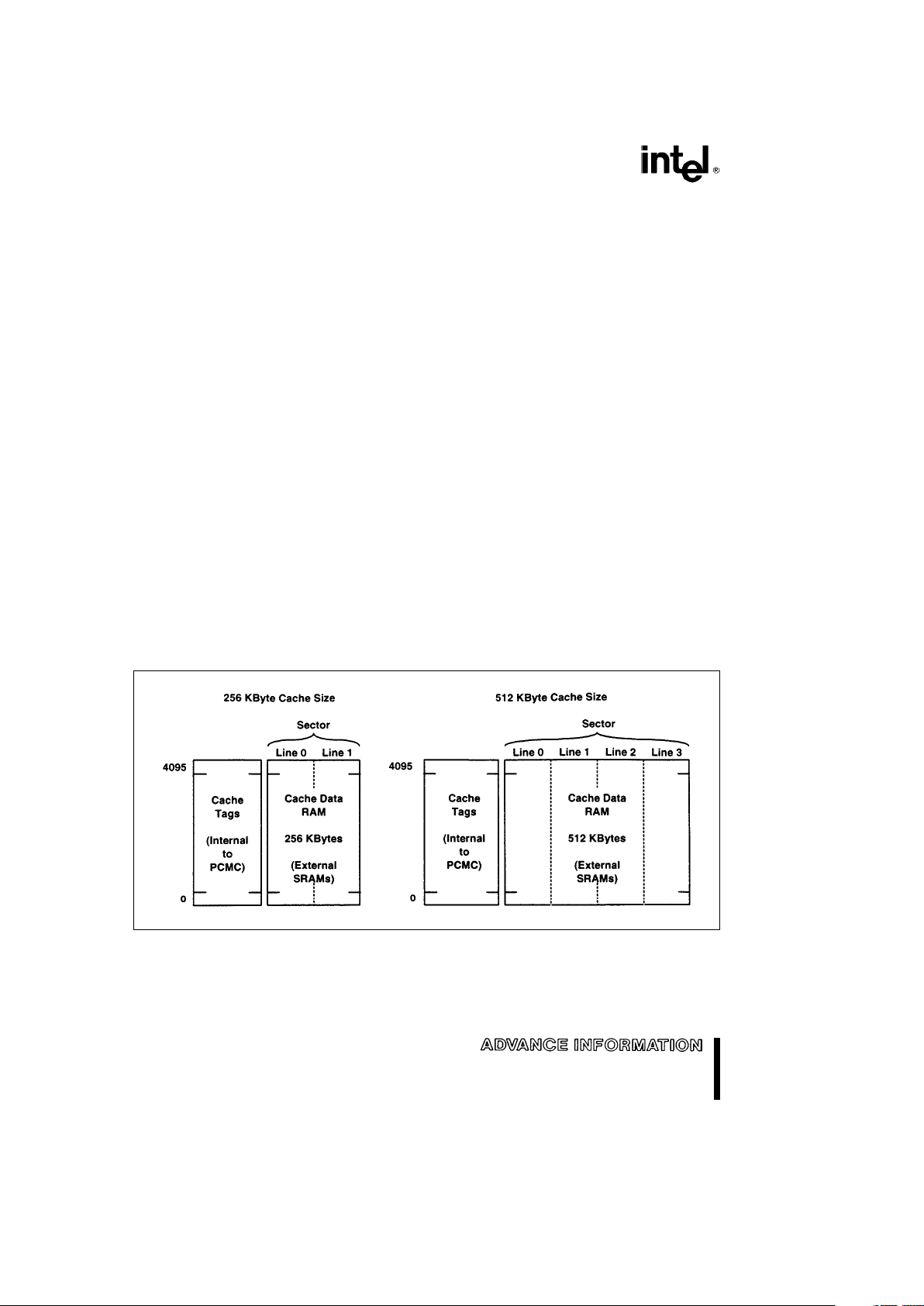
be either 256-KBytes or 512-KBytes in size. The
cache is direct-mapped and is organized as either
8K or 16K cache lines of 32 bytes per line.
In addition to the cache data RAM, the second level
cache contains a 4K set of cache tags that are internal to the PCMC. Each tag contains an address that
is associated with the corresponding data sector
(2 lines for a 256 KByte cache and 4 lines for a
512 KByte cache) and two status bits for each line in
the sector.
During a main memory read or write operation, the
PCMC first searches the cache. If the addressed
code or data is in the cache, the cycle is serviced by
the cache. If the addressed code or data is not in the
cache, the cycle is forwarded to main memory.
For the write-through (82434LX only) and write-back
(both 82434LX and 82434NX) policies, the cache
operation is determined by the CPU read or write
cycle as follows:
Write Cycle
If the caching policy is write-through and the write
cycle hits in the cache, both the cache and main
memory are updated. Upon a cache miss, only
main memory is updated. The cache is not updated (no write-allocate).
If the caching policy is write-back and the write
cycle hits in the cache, only the cache is updated;
main memory is not affected. Upon a cache miss,
only main memory is updated. The cache is not
updated (no write-allocate).
Read Cycle
Upon a cache hit, the cache operation is the same
for both write-through and write-back. In this case,
data is transferred from the cache to the CPU.
Main memory is not accessed.
290479– 4
Figure 3. Second Level Cache Organization
14
Page 15

82434LX/82434NX
If the read cycle causes a cache miss, the line
containing the requested data is transferred from
main memory to the cache and to the CPU. In the
case of a write-back cache, if the cache line fill is
to a sector containing one or more modified lines,
the modified lines are written back to main memory
and the new line is brought into the cache. For a
modified line write-back operation, the PCMC
transfers the modified cache lines to main memory
via a write buffer in the LBX. Before writing the last
modified line from the write buffer to main memory,
the PCMC updates the first and second level
caches with the new line, allowing the CPU access
to the requested data with minimum latency.
1.2.1.1 Cache Consistency
The Snoop mechanism in the PCMC ensures data
consistency between cache (both first level and second level) and main memory. The PCMC monitors
PCI master accesses to main memory and when
needed, initiates an inquire (snoop) cycle to the first
and second level caches. The snoop mechanism
guarantees that consistent data is always delivered
to both the host CPU and PCI masters.
1.2.2 ADDRESS/DATA PATHS
Address paths between the CPU/cache and PCI
and data paths between the CPU/cache, PCI, and
main memory are supplied by two LBX components.
The LBX is a companion component to the PCMC.
Together, they form a Host/PCI bridge. The PCMC
(via the PCMC/LBX interface signals), controls the
address and data flow through the LBXs. Refer to
the LBX data sheet for more details on the address
and data paths.
Data is transferred to and from the PCMC internal
registers via the PCMC address lines. When the
Host CPU performs a write operation, the data is
sent to the LBXs. When the PCMC decodes the cycle as an access to one of its internal registers, it
asserts AHOLD to the CPU and instructs the LBXs
to copy the data onto the Host address lines. When
the PCMC decodes a Host read as an access to a
PCMC internal register, it asserts AHOLD to the
CPU. The PCMC then places the register data on its
address lines and instructs the LBX to copy the data
on the Host address bus to the Host data bus. When
the register data is on the Host data bus, the PCMC
negates AHOLD and completes the cycle.
1.2.2.1 Read/Write Buffers
The LBX provides an interface for the CPU address
and data buses, PCI Address/Data bus, and the
main memory DRAM data bus. There are three posted write buffers and one read-prefetch buffers implemented in the LBXs to increase performance and to
maximize concurrency. The buffers are:
#
CPU-to-Main Memory Posted Write Buffer
(4 Qwords)
#
CPU-to-PCI Posted Write Buffer (4 Dwords)
#
PCI-to-Main Memory Posted Write Buffer (2 x 4
Dwords)
#
PCI-to-Main Memory Read Prefetch Buffer (line
buffer, 4 Qwords).
Refer to the LBX data sheet for details on the operation of these buffers.
1.2.3 HOST/PCI BRIDGE OPERATIONS
The PCMC permits the Host CPU to access devices
on the PCI Bus. These accesses can be to PCI I/O
space, PCI memory space, or PCI configuration
space.
As a PCI device, the PCMC can be either a master
initiating a PCI Bus operation or a target responding
to a PCI Bus operation. The PCMC is a PCI Bus
master for Host-to-PCI cycles and a target for PCIto-main memory transfers. Note that the PCMC does
not permit peripherals to be located on the Host
Bus. CPU I/O cycles, other than to PCMC internal
registers, are forwarded to the PCI Bus and PCI Bus
accesses to the Host Bus are not supported.
When the CPU initiates a bus cycle to a PCI device,
the PCMC becomes a PCI Bus master and translates the CPU cycle into the appropriate PCI Bus
cycle. The Host/PCI Posted write buffer in the LBXs
permits the CPU to complete CPU-to-PCI Dword
memory writes in three CPU clocks (1 wait-state),
even if the PCI Bus is currently busy. The posted
data is written to the PCI device when the PCI Bus is
available.
When a PCI Bus master initiates a main memory access, the PCMC (and LBXs) become the target of
the PCI Bus cycle and responds to the read/write
access. During PCI-to-main memory accesses, the
PCMC automatically performs cache snoop operations on the Host Bus, when needed, to maintain
data consistency.
15
Page 16

82434LX/82434NX
As a PCI device, the PCMC contains all of the required PCI configuration registers. The Host CPU
reads and writes these registers as described in
Section 3.0, Register Description.
1.2.4 DRAM MEMORY OPERATIONS
The PCMC contains a DRAM controller that supports CPU and PCI master accesses to main memory. The PCMC DRAM interface supplies the control
signals and address lines and the LBXs supply the
data path. DRAM parity is generated for main memory writes and checked for memory reads.
For the 82434LX, the memory array is 64-bits wide
and ranges in size from 2 MBytes– 192 MBytes. The
array can be implemented with either single-sided or
double-sided SIMMs. DRAM SIMM sizes of 256K x
36, 1M x 36, and 4M x 36 are supported.
For the 82434NX, the memory array is 64-bits wide
and ranges in size from 2 MBytes– 512 MBytes. The
array can be implemented with either single-sided or
double-sided SIMMs. DRAM SIMM sizes of 256K x
36, 1M x 36, 4M x 36, and 16M x 36 are supported.
To provide optimum support for the various cache
configurations, and the resultant mix of bus cycles,
the system designer can select between 0-active
RAS
Ý
and 1-active RASÝmodes. These modes af-
fect the behavior of the RAS
Ý
signal following either
CPU-to-main memory cycles or PCI-to-main memory
cycles.
The PCMC also provides programmable memory
and cacheability attributes on 14 memory segments
of various sizes in the ISA compatibility range
(512 KByte – 1 MByte address range). Access rights
to these memory segments from the PCI Bus are
controlled by the expansion bus bridge.
The PCMC permits a gap to be created in main
memory within the 1 MByte – 16 MBytes address
range, accommodating ISA devices which are
mapped into this range (e.g., ISA LAN card or an ISA
frame buffer).
1.2.5 3.3V SIGNALS
The 82434NX PCMC drives 3.3V signal levels on the
CPU and second level cache interfaces. Thus, no
extra logic (i.e. 5V/3.3V translation) is required when
interfacing to 3.3V processors and SRAMs. Six of
the power pins on the 82434NX are VDD3 pins.
These pins are connected to a 3.3V power supply.
The VDD3 pins power the output buffers on the CPU
and second level cache interfaces. The VDD3 pins
also power the output buffers for the HCLK[A-F
]
outputs.
2.0 SIGNAL DESCRIPTIONS
This section provides a detailed description of each
signal. The signals are arranged in functional groups
according to their associated interface. The states of
all of the signals during hard reset are provided in
Section 8.0, System Clocking and Reset.
The ‘‘
Ý
’’ symbol at the end of a signal name indicates that the active, or asserted state occurs when
the signal is at a low voltage level. When ‘‘
Ý
’’ is not
present after the signal name, the signal is asserted
when at the high voltage level.
The terms assertion and negation are used extensively. This is done to avoid confusion when working
with a mixture of ‘‘active-low’’ and ‘‘active-high’’ signals. The term assert,orassertion indicates that a
signal is active, independent of whether that level is
represented by a high or low voltage. The term ne-
gate,ornegation indicates that a signal is inactive.
The following notations are used to describe the signal type.
in Input is a standard input-only signal
out Totem pole output is a standard active driver
o/d Open drain
t/s Tri-State is a bi-directional, tri-state input/out-
put pin
s/t/s Sustained tri-state is an active low tri-state sig-
nal owned and driven by one and only one
agent at a time. The agent that drives a s/t/s
pin low must drive it high for at least one clock
before letting it float. A new agent can not
start driving a s/t/s signal any sooner than
one clock after the previous owner tri-states it.
An external pull-up is required to sustain the
inactive state until another agent drives it and
must be provided by the central resource.
16
Page 17
82434LX/82434NX
2.1 Host Interface
Signal Type Description
A[31:0]t/s ADDRESS BUS: A[31:0]are the address lines of the Host Bus. A[31:3]are connected to
the CPU A[31:3]lines and to the LBXs. A[2:0]are only connected to the LBXs. Along with
the byte enable signals, the A[31:3]lines define the physical area of memory or I/O being
accessed. During CPU cycles, the A[31:3]lines are inputs to the PCMC. They are used for
address decoding and second level cache tag lookup sequences. Also during CPU cycles,
A[2:0]are outputs and are generated from BE[7:0
]
Ý
.A[27:24]provide hardware
strapping options for test features. For more details on theses options, refer to Section
11.0 Testability.
During inquire cycles, A[31:5]are inputs from the LBXs to the CPU and the PCMC to
snoop the first and the second level cache tags, respectively. In response to a Flush or
Flush Acknowledge Special Cycle, the PCMC asserts AHOLD and drives the addresses of
the second level cache lines to be written back to main memory on A[18:7].
During CPU to PCI configuration cycles, the PCMC drives A[31:0]with the PCI
configuration space address that is internally derived from the CPU physical I/O address.
All PCMC internal configuration registers are accessed via A[31:0]. During CPU reads
from PCMC internal configuration registers, the PCMC asserts AHOLD and drives the
contents of the addressed register on A[31:0]. The PCMC then signals the LBXs to copy
this value from the address lines onto the host data lines. During writes to PCMC internal
configuration registers, the PCMC asserts AHOLD and signals the LBXs to copy the write
data onto the A[31:0]lines.
Finally, when in deturbo mode, the PCMC periodically asserts AHOLD and then drives
A[31:0]to valid logic levels to keep these lines from floating for an extended period of
time.
A[31:28]provide hardware strapping options at powerup. For more details on strapping
options, refer to Section 8.0, System Clocking and Reset. A[27:24]provide hardware
strapping options for test features. For more details on these options, refer to Section
11.0 Testability.
17
Page 18
82434LX/82434NX
Signal Type Description
BE[7:0
]
Ý
in BYTE ENABLES: The byte enables indicate which byte lanes on the CPU data bus
carry valid data during the current bus cycle. In the case of cacheable reads, all 8 bytes
of data are driven to the Pentium processor, regardless of the state of the byte enables.
The byte enable signals indicate the type of special cycle when M/IO
Ý
e
D/C
Ý
e
0 and
W/R
Ý
e
1. During special cycles, only one byte enable is asserted by the CPU. The
following table depicts the special cycle types and their byte enable encodings:
Special Cycle Type Asserted Byte Enable
Shutdown BE0
Ý
Flush BE1
Ý
Halt/Stop Grant BE2
Ý
Write Back BE3
Ý
Flush Acknowledge BE4
Ý
Branch Trace Message BE5
Ý
When the PCMC decodes a Shutdown Special Cycle, it asserts AHOLD, drives
000...000 (the PCI Shutdown Special Cycle Encoding) on the A[31:0]lines and signals
the LBXs to latch the host address bus. The PCMC then drives a Special Cycle on PCI,
signaling the LBXs to drive the latched address (00...00) on the AD[31:0]lines during
the data phase. The PCMC then asserts INIT for 16 HCLKs.
In response to Flush and Flush Acknowledge Special Cycles, the PCMC internally
inspects the Valid and Modified bits for each of the Second Level Cache Sectors. If a
line is both valid and modified, the PCMC drives the cache address of the line on the
A[18:7]and CAA/CAB[6:3]lines and writes the line back to main memory. The valid
and modified bits are both reset to 0. All valid and unmodified lines are simply marked
invalid.
In response to a write back special cycle, the PCMC simply returns BRDY
Ý
to the CPU.
The second level cache will be written back to main memory in response to the
following flush special cycle.
If BE2Ýis asserted during a special cycle, the 82434NX uses A4 to determine if the
cycle is a Halt or Stop Grant Special Cycle. If A4
e
0, the cycle is a Halt Special Cycle
and if A4
e
1, the cycle is a Stop Grant Special cycle.
In response to a halt special cycle, the PCMC asserts AHOLD, drives 000...001 (the PCI
halt special cycle encoding) on the A[31:0]lines, and signals the LBXs to latch the host
address bus. The PCMC then drives a special cycle on PCI, signaling the LBXs to drive
the latched address (00...01) on the AD[31:0]lines during the data phase.
When the 82434NX PCMC detects a CPU Stop Grant Special Cycle (M/IO
Ý
e
0,
D/C
Ý
e
0, W/R
Ý
e
1, A4e1, BE[7:0
]
Ý
e
FBh), it generates a PCI Stop Grant Special
cycle, with 0002h in the message field (AD[15:0]) and 0012h in the message dependent
data field (AD[31:16]) during the first data phase (IRDY
Ý
asserted).
ADS
Ý
in ADDRESS STROBE: The Pentium processor asserts ADSÝto indicate that a new bus
cycle is beginning. ADS
Ý
is driven active in the same clock as the address, byte enable,
and cycle definition signals. The PCMC ignores a floating low ADSÝthat may occur
when BOFF
Ý
is asserted as the CPU is asserting ADSÝ.
18
Page 19
82434LX/82434NX
Signal Type Description
BRDYÝout BURST READY: BRDYÝindicates that the system has responded in one of three ways:
1. valid data has been placed on the Pentium processor data pins in response to a read,
2. CPU write data has been accepted by the system, or
3. the system has responded to a special cycle.
NA
Ý
out NEXT ADDRESS: The PCMC asserts NAÝfor one clock when the memory system is
ready to accept a new address from the CPU, even if all data transfers for the current
cycle have not completed. The CPU may drive out a pending cycle two clocks after NA
Ý
is asserted and has the ability to support up to two outstanding bus cycles.
AHOLD out ADDRESS HOLD: The PCMC asserts AHOLD to force the Pentium processor to stop
driving the address bus so that either the PCMC or LBXs can drive the bus. During PCI
master cycles, AHOLD is asserted to allow the LBXs to drive a snoop address onto the
address bus. If the PCI master locks main memory, AHOLD remains asserted until the
PCI master locked sequence is complete and the PCI master negates PLOCKÝ.
AHOLD is asserted during all accesses to PCMC internal configuration registers to allow
configuration register accesses to occur over the A[31:0]lines.
When in deturbo mode, the PCMC periodically asserts AHOLD to prevent the processor
from initiating bus cycles in order to emulate a slower system. The duration of AHOLD
assertion in deturbo mode is controlled by the Deturbo Frequency Control Register
(offset 51h). When PWROK is negated, the PCMC asserts AHOLD to allow the strapping
options on A[31:28]to be read. For more details on strapping options, see the System
Clocking and Reset section.
EADSÝout EXTERNAL ADDRESS STROBE: The PCMC asserts EADSÝto indicate to the Pentium
processor that a valid snoop address has been driven onto the CPU address lines to
perform an inquire cycle. During PCI master cycles, the PCMC signals the LBXs to drive a
snoop address onto the host address lines and then asserts EADS
Ý
to cause the CPU to
sample the snoop address.
INV out INVALIDATE: The INV signal specifies the final state (invalid or shared) that a first level
cache line transitions to in the event of a cache line hit during a snoop cycle. When
snooping the caches during a PCI master write, the PCMC asserts INV with EADS
Ý
.
When INV is asserted with EADS
Ý
, an inquire hit results in the line being invalidated.
When snooping the caches during a PCI master read, the PCMC does not assert INV with
EADS
Ý
. In this case, an inquire cycle hit results in a line transitioning to the shared state.
BOFF
Ý
out BACKOFF: The PCMC asserts BOFFÝto force the Pentium processor to abort all
outstanding bus cycles that have not been completed and float its bus in the next clock.
The PCMC uses this signal to force the CPU to re-order a write-back due to a snoop cycle
around a currently outstanding bus cycle. The PCMC also asserts BOFF
Ý
to obtain the
CPU data bus for write-back cycles from the secondary cache due to a snoop hit. The
CPU remains in bus hold until BOFF
Ý
is negated.
HITM
Ý
in HIT MODIFIED: The Pentium processor asserts HITMÝto inform the PCMC that the
current inquire cycle hit a modified line. HITM
Ý
is asserted by the Pentium processor two
clocks after the assertion of EADS
Ý
if the inquire cycle hits a modified line in the primary
cache.
19
Page 20
82434LX/82434NX
Signal Type Description
M/IO
Ý
in BUS CYCLE DEFINITION (MEMORY/INPUT-OUTPUT, DATA/CONTROL, WRITE/
READ): M/IO, D/C
Ý
and W/RÝdefine Host Bus cycles as shown in the table below.
D/C
Ý
W/R
Ý
M/IOÝD/CÝW/RÝBus Cycle Type
Low Low Low Interrupt Acknowledge
Low Low High Special Cycle
Low High Low I/O Read
Low High High I/O Write
High Low Low Code Read
High Low High Reserved
High High Low Memory Read
High High High Memory Write
Interrupt acknowledge cycles are forwarded to the PCI Bus as PCI interrupt
acknowledge cycles (i.e. C/BE[3:0
]
Ý
e
0000 during the address phase). All I/O cycles
and any memory cycles that are not directed to memory controlled by the PCMC DRAM
controller are forwarded to PCI. The Pentium processor generates six different types of
special cycles. The special cycle type is encoded on the BE[7:0
]
Ý
lines.
HLOCK
Ý
in HOST BUS LOCK: The Pentium processor asserts HLOCKÝto indicate the current bus
cycle is locked. HLOCK
Ý
is asserted in the first clock of the first locked bus cycle and is
negated after the BRDYÝis returned for the last locked bus cycle. The Pentium
processor guarantees HLOCK
Ý
to be negated for at least one clock between back-toback locked operations. When a CPU locked cycle is directed to main memory, the
PCMC guarantees that once the locked operation begins in main memory, the CPU has
exclusive access to main memory (i.e., PCI master accesses to main memory will not be
initiated until the CPU locked operation completes). When a CPU locked cycle is
directed to PCI, the PCMC arbitrates for PLOCK
Ý
(PCI LOCKÝ) before initiating the
cycle on PCI, except when the cycle is to the memory range defined by the Frame
Buffer Range Register and the No Lock Requests bit in that register is set to 1.
CACHE
Ý
in CACHEABILITY: The Pentium processor asserts CACHEÝto indicate the internal
cacheability of a read cycle or that a write cycle is a burst write-back cycle. If the CPU
drives CACHE
Ý
inactive during a read cycle, the returned data is not cached,
regardless of the state of KEN
Ý
. The CPU asserts CACHEÝfor cacheable data reads,
cacheable code fetches, and cache line write-backs. CACHE
Ý
is driven along with the
cycle definition pins.
KEN
Ý
out CACHE ENABLE: The PCMC asserts KENÝto indicate to the CPU that the current
cycle is cacheable. KEN
Ý
is asserted for all accesses to memory ranges 0–512-KBytes
and 1024-KBytes to the top of main memory controlled by the PCMC when the Primary
Cache Enable bit is set to 1, except in the following case: KEN
Ý
is not asserted for
accesses to the top 64-KByte of main memory controlled by the PCMC when the
SMRAM Enable bit in the DRAM Control Register (Offset 57h) is set to 1 and the area is
not write protected. If the area is write protected and cacheable, KEN
Ý
is asserted for
code read cycles, but is not asserted during data read cycle. KENÝis asserted for any
CPU access within the range of 512-KBytes–1024-KBytes if the corresponding Cache
Enable bit in the PAM[6:0]Registers (offsets 59h–5Fh) is set to 1. When the Pentium
processor indicates that the current read cycle can be cached by asserting CACHE
Ý
and the PCMC responds with KENÝ, the cycle is converted into a burst cache line fill.
The CPU samples KEN
Ý
with the first of either BRDYÝor NAÝ.
20
Page 21
82434LX/82434NX
Signal Type Description
SMIACT
Ý
in SYSTEM MANAGEMENT INTERRUPT ACTIVE: The Pentium processor asserts
SMIACT
Ý
to indicate that the processor is operating in System Management Mode
(SMM). When the SMRAM Enable bit in the DRAM Control Register (offset 57h) is set
to 1, the PCMC allows CPU accesses SMRAM as permitted by the SMRAM Space
Register at configuration space offset 72h.
PEN
Ý
out PARITY ENABLE: The PENÝsignal, along with the MCE bit in CR4 of the Pentium
processor, determines whether a machine check exception will be taken by the CPU as
a result of a parity error on a read cycle. The PCMC asserts PEN
Ý
during DRAM read
cycles if the MCHK on DRAM/L2 Cache Data Parity Error Enable bit in the Error
Command Register (offset 70h) is set to 1. The PCMC asserts PEN
Ý
during CPU
second level cache read cycles if the MCHK on DRAM/L2 Cache Data Parity Error
Enable and the L2 Cache Parity Enable bits in the Error Command Register (offset 70h)
are both set to 1.
PCHK
Ý
in DATA PARITY CHECK: PCHKÝis sampled by the PCMC to detect parity errors on
CPU read cycles from main memory if the Parity Error Mask Enable bit in the DRAM
Control Register (offset 57h) is reset to 0. PCHK
Ý
is sampled by the PCMC to detect
parity errors on CPU read cycles from the second level cache if the L2 Cache Parity
Enable bit in the Error Command Register (offset 70h) is set to 1. If incorrect parity was
detected on a data read, the PCHK
Ý
signal is asserted by the Pentium processor two
clocks after BRDY
Ý
is returned. PCHKÝis asserted for one clock for each clock in
which a parity error was detected.
21
Page 22
82434LX/82434NX
2.2 DRAM Interface
Signal Type Description
RAS[5:0
]
Ý
out ROW ADDRESS STROBES: The RAS[5:0
]
Ý
signals are used to latch the row
address on the MA[10:0]lines into the DRAMs. Each RAS[5:0
]
Ý
signal corresponds
to one DRAM row. The 82434LX PCMC supports up to 6 rows in the DRAM array.
Each row is eight bytes wide. These signals drive the RAS
Ý
lines of the DRAM array
directly, without external buffers.
RAS[7:6
]
Ý
out ROW ADDRESS STROBES: The 82434NX supports up to eight rows of DRAM.
RAS[7:6
]
Ý
are used with RAS[5:0]to latch the row address on the MA[11:0]lines
into the DRAMs. Each row is eight bytes wide. These signals drive the RAS
Ý
lines of
the DRAM array directly, without external buffers.
CAS[7:0
]
Ý
out COLUMN ADDRESS STROBES: The CAS[7:0
]
Ý
signals are used to latch the
column address on the MA[10:0]lines into the DRAMs. Each CAS[7:0
]
Ý
signal
corresponds to one byte of the eight byte-wide array. These signals drive the CAS
Ý
lines of the DRAM array directly, without external buffers. In a minimum configuration,
each CAS[7:0
]
Ý
line only has one SIMM load, while the maximum configuration has 6
SIMM loads.
WE
Ý
out DRAM WRITE ENABLE: WEÝis asserted during both CPU and PCI master writes to
main memory. During burst writes to main memory, WE
Ý
is asserted before the first
assertion of CAS[7:0
]
Ý
and is negated with the last CAS[7:0
]
Ý
. The WEÝsignal is
externally buffered to drive the WE
Ý
inputs on the DRAMs.
MA[10:0
]
out DRAM MULTIPLEXED ADDRESS: MA[10:0]provide the row and column address to
the DRAM array. The 82434LX uses MA[10:0]for the complete DRAM address bus.
The MA[10:0]lines are externally buffered to drive the multiplexed address lines of
the DRAM array.
MA11 out DRAM MULTIPLEXED ADDRESS: MA11 provides the extra addressability for the
16M x 36 SiMMs that are supported by the 82434NX. MA[11:0]provide the row and
column address to the DRAM array. Like MA[10:0], MA11 is externally buffered to
drive the multiplexed address lines of the DRAM array.
22
Page 23
82434LX/82434NX
2.3 Cache Interface
Signal Type Description
CALE out CACHE ADDRESS LATCH ENABLE: CALE controls the external latch between the
host address lines and the cache address lines. CALE is asserted to open the
external latch, allowing the host address lines to propagate to the cache address
lines. CALE is negated to latch the cache address lines.
CADS[1:0
]
Ý
, out This signal pin has two functions, depending on the type of SRAMs used for the
second level cache.
CR/W[1:0
]
Ý
CACHE ADDRESS STROBE: CADS[1:0
]
Ý
are used with burst SRAMs. When
asserted, CADS[1:0
]
Ý
cause the burst SRAMs to latch the cache address on the
rising edge of HCLK. CADS[1:0
]
Ý
are glitch-free synchronous signals. CADS[1:0
]
Ý
functionality is selected by the SRAM type bit in the Secondary Cache Control
Register. Two copies of this signal are provided for timing reasons only.
CACHE READ/WRITE: CR/W
Ý
provide read/write control to the second level
cache when using asynchronous dual-byte select SRAMs. This functionality is
selected by the SRAM Type and Cache Byte Control Bits in the Secondary Cache
Control Register. The two copies of this signal are always driven to the same logic
level.
CADV[1:0
]
Ý
, out This signal pin has two functions. The Cache Chip Select function is only enabled
when the SRAM connectivity bit (bit 2) in the SCC Register is set to 1.
CCS[1:0
]
Ý
CACHE ADVANCE: CADV[1:0
]
Ý
are used with burst SRAMs to advance the
internal two bit address counter inside the SRAMs to the next address of the burst
sequence. Two copies of this signal are provided for timing reasons only. The two
copies are always driven to the same logic level.
CACHE CHIP SELECT: CCS[1:0
]
Ý
are used with asynchronous SRAMs to deselect the SRAMs, placing them in a low power standby mode. When the CPU runs
a halt or stop grant special cycle, the 82434NX negates CCS[1:0
]
Ý
, placing the
second level cache in a power saving mode. The PCMC then asserts CCS[1:0
]
Ý
(activating the SRAMs) when the CPU asserts ADSÝ.
When using burst SRAMs, only CCS1Ýimplements the CCSÝfunction. CADV0
Ý
retains the address advance function. CCS1Ýserve two purposes with burst
SRAMs: 1) It is used (along with CADS[1:0
]
Ý
) to place the SRAMs in a low power
standby mode. When the CPU runs a halt or stop grant special cycle, the 82434NX
negates CCS1
Ý
and asserts CADS[1:0
]
Ý
for one clock, placing the SRAMs in a
power saving mode. The PCMC then asserts CCS1
Ý
so that the next ADSÝfrom
the CPU places the SRAMs in an active mode. 2) CCS1
Ý
is used to block pipelined
cycles from the SRAMs when the SRAMs are servicing a cycle. After NA
Ý
is
asserted, the PCMC negates CCS1Ýpreventing the SRAMs from sampling a new
address. CCS1
Ý
is asserted again when the SRAMs have completed the current
cycle.
CAA[6:3
]
out CACHE ADDRESS[6:3]: CAA[6:3]and CAB[6:3]are connected to address lines
A[3:0]on the second level cache SRAMs. CAA[4:3]and CAB[4:3]are used with
CAB[6:3
]
standard SRAMs to advance through the burst sequence. CAA[6:5]and CAB[6:5
]
are used during second level cache write-back cycles to address the modified lines
within the addressed sector. Two copies of these signals are provided for timing
reasons only. The two copies are always driven to the same logic level.
23
Page 24
82434LX/82434NX
Signal Type Description
COE[1:0
]
Ý
out CACHE OUTPUT ENABLE: COE[1:0
]
Ý
are asserted when data is to be read from
the second level cache and are negated at all other times. Two copies of this signal
are provided for timing reasons only. The two copies are always driven to the same
logic level.
CWE[7:0
]
Ý
, out This signal pin has two functions, depending on the type of SRAMs used for the
second level cache.
CBS[7:0
]
Ý
CACHE WRITE ENABLES: CWE[7:0
]
Ý
are asserted to write data to the second
level cache SRAMs on a byte-by-byte basis. CWE7
Ý
controls the most significant
byte while CWE0
Ý
controls the least significant byte. These signals are cache write
enables when using burst SRAMs (SRAM Type bit in SCC Register is 1) or when
using asynchronous SRAMs (SRAM Type bit in SCC Register is 0) and the Cache
Byte Control Bit is 1.
CACHE BYTE SELECTS: The CBS[7:0
]
Ý
lines provide byte control to the
secondary cache when using dual-byte select asynchronous SRAMs. These signals
are Cache Byte select lines when the SRAM Type and Cache Byte Control Bits in the
SCC Register are both 0.
2.4 PCI Interface
Signal Type Description
C/BE[3:0
]
Ý
t/s PCI BUS COMMAND AND BYTE ENABLES: C/BE[3:0
]
Ý
are driven by the current
bus master during the address phase of a PCI cycle to define the PCI command, and
during the data phase as the PCI byte enables. The PCI commands indicate the
current cycle type, and the PCI byte enables indicate which byte lanes carry
meaningful data. C/BE[3:0
]
Ý
are outputs of the PCMC during CPU cycles that are
directed to PCI. C/BE[3:0
]
Ý
are inputs when the PCMC acts as a slave. The
command encodings and types are listed below.
C/BE[3:0
]
Ý
Command
0000 Interrupt Acknowledge
0001 Special Cycle
0010 I/O Read
0011 I/O Write
0100 Reserved
0101 Reserved
0110 Memory Read
0111 Memory Write
1000 Reserved
1001 Reserved
1010 Configuration Read
1011 Configuration Write
1100 Memory Read Multiple
1101 Reserved
1110 Memory Read Line
1111 Memory Write and Invalidate
24
Page 25
82434LX/82434NX
Signal Type Description
FRAMEÝs/t/s CYCLE FRAME: FRAMEÝis driven by the current bus master to indicate the
beginning and duration of an access. FRAME
Ý
is asserted to indicate that a bus
transaction is beginning. While FRAME
Ý
is asserted, data transfers continue. When
FRAME
Ý
is negated, the transaction is in the final data phase. FRAMEÝis an output
of the PCMC during CPU cycles which are directed to PCI. FRAME
Ý
is an input to the
PCMC when the PCMC acts as a slave.
IRDY
Ý
s/t/s INITIATOR READY: The assertion of IRDYÝindicates the current bus master’s ability
to complete the current data phase. IRDY
Ý
works in conjunction with TRDYÝto
indicate when data has been transferred. On PCI, data is transferred on each clock
that both IRDY
Ý
and TRDYÝare asserted. During read cycles, IRDYÝis used to
indicate that the master is prepared to accept data. During write cycles, IRDY
Ý
is used
to indicate that the master has driven valid data on the AD[31:0]lines. Wait states are
inserted until both IRDY
Ý
and TRDYÝare asserted together. IRDYÝis an output of
the PCMC when the PCMC is the PCI master. IRDYÝis an input to the PCMC when
the PCMC acts as a slave.
TRDY
Ý
s/t/s TARGET READY: TRDYÝindicates the target device’s ability to complete the current
data phase of the transaction. It is used in conjunction with IRDY
Ý
. A data phase is
completed on each clock that TRDY
Ý
and IRDYÝare both sampled asserted. During
read cycles, TRDY
Ý
indicates that valid data is present on AD[31:0]lines. During write
cycles, TRDY
Ý
indicates the target is prepared to accept data. Wait states are
inserted on the bus until both IRDY
Ý
and TRDYÝare asserted together. TRDYÝis an
output of the PCMC when the PCMC is the PCI slave. TRDYÝis an input to the PCMC
when the PCMC is a master.
DEVSELÝs/t/s DEVICE SELECT: When asserted, DEVSELÝindicates that the driving device has
decoded its address as the target of the current access. DEVSEL
Ý
is an output of the
PCMC when PCMC is a PCI slave and is derived from the MEMCS
Ý
input. MEMCS
Ý
is generated by the expansion bus bridge as a decode to the main memory address
space. During CPU-to-PCI cycles, DEVSEL
Ý
is an input. It is used to determine if any
device has responded to the current bus cycle, and to detect a target abort cycle.
Master-Abort termination results if no subtractive decode agent exists in the system,
and no one asserts DEVSEL
Ý
within a programmed number of clocks.
STOP
Ý
s/t/s STOP: STOPÝindicates that the current target is requesting the master to stop the
current transaction. This signal is used in conjunction with DEVSEL
Ý
to indicate
disconnect, target-abort, and retry cycles. When PCMC is acting as a master on PCI, if
STOP
Ý
is sampled active on a rising edge of PCLKIN, FRAMEÝis negated within a
maximum of 3 clock cycles. STOPÝmay be asserted by the PCMC in three cases. If a
PCI master attempts to access main memory when another PCI master has locked
main memory, the PCMC asserts STOP
Ý
to signal retry. The PCMC detects this
condition when sampling FRAME
Ý
and LOCKÝboth active during an address phase.
When a PCI master is reading from main memory, the PCMC asserts STOP
Ý
when the
burst cycle is about to cross a cache line boundary. When a PCI master is writing to
main memory, the PCMC asserts STOP
Ý
upon filling either of the two PCI-to-main
memory posted write buffers. Once asserted, STOP
Ý
remains asserted until FRAME
Ý
is negated.
25
Page 26
82434LX/82434NX
Signal Type Description
PLOCK
Ý
s/t/s PCI LOCK: PLOCKÝis used to indicate an atomic operation that may require
multiple transactions to complete. PCI provides a mechanism referred to as
‘‘resource lock’’ in which only the target of the PCI transaction is locked. The
assertion of GNT
Ý
on PCI does not guarantee control of the PLOCKÝsignal.
Control of PLOCK
Ý
is obtained under its own protocol. When the PCMC is the PCI
slave, PLOCK
Ý
is sampled as an input on the rising edge of PCLKIN when FRAME
Ý
is sampled active. If PLOCKÝis sampled asserted, the PCMC enters into a locked
state and remains in the locked state until PLOCK
Ý
is sampled negated on a
following rising edge of PCLKIN, when FRAME
Ý
is sampled asserted.
REQ
Ý
out REQUEST: The PCMC asserts REQÝto indicate to the PCI bus arbiter that the
PCMC is requesting use of the PCI Bus in response to a CPU cycle directed to PCI.
GNT
Ý
in GRANT: When asserted, GNTÝindicates that access to the PCI Bus has been
granted to the PCMC by the PCI Bus arbiter.
MEMCS
Ý
in MAIN MEMORY CHIP SELECT: When asserted, MEMCSÝindicates to the PCMC
that a PCI master cycle is targeting main memory. MEMCS
Ý
is generated by the
expansion bus bridge. MEMCS
Ý
is sampled by the PCMC on the rising edge of
PCLKIN on the first and second cycle after FRAME
Ý
has been asserted.
FLSHREQ
Ý
in FLUSH REQUEST: When asserted, FLSHREQÝinstructs the PCMC to flush the
CPU-to-PCI posted write buffer in the LBXs and to disable further posting to this
buffer as long as FLSHREQÝremains active. The PCMC acknowledges completion
of the CPU-to-PCI write buffer flush operation by asserting MEMACK
Ý
. MEMACK
Ý
remains asserted until FLSHREQÝis negated. FLSHREQÝis driven by the
expansion bus bridge and is used to avoid deadlock conditions on the PCI Bus.
MEMREQ
Ý
in MEMORY REQUEST: When asserted, MEMREQÝinstructs the PCMC to flush the
CPU-to-PCI and CPU-to-main memory posted write buffers and to disable posting in
these buffers as long as MEMREQ
Ý
is active. The PCMC acknowledges completion
of the flush operations by asserting MEMACK
Ý
. MEMACKÝremains asserted until
MEMREQÝis negated. MEMREQÝis driven by the expansion bus bridge.
MEMACK
Ý
out MEMORY ACKNOWLEDGE: When asserted, MEMACKÝindicates the completion
of the operations requested by an active FLSHREQ
Ý
and/or MEMREQÝ.
PAR t/s PARITY: PAR is an even parity bit across the AD[31:0]and C/BE[3:0
]
Ý
lines. Parity
is generated on all PCI transactions. As a master, the PCMC generates even parity
on CPU writes to PCI, based on the PPOUT[1:0]inputs from the LBXs. During CPU
read cycles from PCI, the PCMC checks parity by checking the value sampled on the
PAR input with the PPOUT[1:0]inputs from the LBXs. As a slave, the PCMC
generates even parity on PAR, based on the PPOUT[1:0]inputs during PCI master
reads from main memory. During PCI master writes to main memory, the PCMC
checks parity by checking the value sampled on PAR with the PPOUT[1:0]inputs.
26
Page 27
82434LX/82434NX
Signal Type Description
PERRÝs/t/s PARITY ERROR: PERRÝmay be pulsed by any agent that detects a parity error during
an address phase, or by the master or the selected target during any data phase in which
the AD lines are inputs. The PERR
Ý
signal is enabled when the PERRÝon Receiving
Data Parity Error bit in the Error Command Register (offset 70h) and the Parity Error
Enable bit in the PCI Command Register (offset 04h) are both set to 1.
When enabled, CPU-to-PCI write data is checked for parity errors by sampling the
PERR
Ý
signal two PCI clocks after data is driven. Also, when enabled, PERRÝis
asserted by the PCMC when it detects a data parity error on CPU read data from PCI and
PCI master write data to main memory. PERR
Ý
is neither sampled nor driven by the
PCMC when either the PERR
Ý
on Receiving Data Parity Error bit in the Error Command
Register or the Parity Error Enable bit in the PCI Command Register is reset to 0.
SERRÝo/d SYSTEM ERROR: SERRÝmay be pulsed by any agent for reporting errors other than
parity. SERR
Ý
is asserted by the PCMC whenever a serious system error (not
necessarily a PCI error) occurs. The intent is to have the PCI central agent (for example,
the expansion bus bridge) assert NMI to the processor. Control over the SERR
Ý
signal is
provided via the Error Command Register (offset 70h) when the Parity Error Enable bit in
the PCI Command Register (offset 04h) is set to 1. When the SERR
Ý
DRAM/L2 Cache
Data Parity Error bit is set to 1, SERR
Ý
is asserted upon detecting a parity error on CPU
read cycles from DRAM. If the L2 Cache Parity bit is also set to 1, SERR
Ý
will be
asserted upon detecting a parity error on CPU read cycles from the second level cache.
The Pentium processor indicates these parity errors to the PCMC via the PCHK
Ý
signal.
When the SERRÝon PCI Address Parity Error bit is set to 1, the PCMC asserts SERRÝif
a parity error is detected during the address phase of a PCI master cycle.
When the SERR
Ý
on Received PCI Data Parity bit is set to 1, the PCMC asserts SERR
Ý
if a parity error is detected on PCI during a CPU read from PCI. During CPU to PCI write
cycles, when the SERR
Ý
on Transmitted PCI Data Parity Error bit is set to 1, the PCMC
asserts SERR
Ý
in response to sampling PERRÝactive. When the SERRÝon Received
Target Abort bit is set to 1, the PCMC asserts SERR
Ý
when the PCMC receives a target
abort on a PCMC initiated PCI cycle. If the Parity Error Enable bit in the PCI Command
Register is reset to 0, SERR
Ý
is disabled and is never asserted by the PCMC.
27
Page 28
82434LX/82434NX
2.5 LBX Interface
Signal Type Description
HIG[4:0
]
out HOST INTERFACE GROUP: HIG[4:0]are outputs of the PCMC used to control the
LBX HA (Host Address) and HD (Host Data) buses. Commands driven on HIG[4:0
]
cause the host data and/or address lines to be either driven or latched by the LBXs.
See the 82433LX (LBX) Local Bus Accelerator Data Sheet for a listing of the
HIG[4:0]commands.
MIG[2:0
]
out MEMORY INTERFACE GROUP: MIG[2:0]are outputs of the PCMC and control the
LBX MD (Memory Data) bus. Commands driven on the MIG[2:0]lines cause the
memory data lines to be either driven or latched by the LBXs. See the 82433LX (LBX)
Local Bus Accelerator Data Sheet for a listing of the MIG[2:0]commands.
MDLE out MEMORY DATA LATCH ENABLE: During CPU reads from main memory, MDLE is
used to control the latching of memory read data on the CPU data bus. MDLE is
negated as CAS[7:0
]
Ý
are negated to close the latch between the memory data bus
and the host data bus. During CPU reads from main memory, the PCMC closes the
memory data to host data latch in the LBXs as BRDYÝis asserted and opens the
latch after the CPU has sampled the data.
PIG[3:0
]
out PCI INTERFACE GROUP: PIG[3:0]are outputs of the PCMC used to control the LBX
AD (PCI Address/Data) bus. Commands driven on the PIG[3:0]lines cause the AD
lines to be either driven or latched. See the 82433LX (LBX) Local Bus Accelerator
Data Sheet for a listing of the PIG[3:0]commands.
DRVPCI out DRIVE PCI: DRVPCI acts as an output enable for the LBX AD lines. When sampled
asserted, the LBXs begin driving the PCI AD lines. When negated, the AD lines on
the LBXs are tri-stated. The LBX AD lines are tri-stated asynchronously from the
falling edge of DRVPCI.
EOL in END OF LINE: EOL is asserted by the low order LBX when a PCI master read or
write transaction is about to overrun a cache line boundary. EOL has an internal pullup resistor inside the PCMC. The low order LBX EOL signal connects to this PCMC
input. The high order LBX EOL signal is connected to ground through an external
pull-down resistor.
PPOUT[1:0]in PCI PARITY OUT: These signals reflect the parity of the 32 AD lines driven from or
latched in the LBXs, depending on the command driven on PIG[3:0]. The PPOUT0
pin has a weak internal pull-down resistor. The PPOUT1 pin has a weak internal pullup resistor.
2.6 Reset And Clock
Signal Type Description
HCLKOSC in HOST CLOCK OSCILLATOR: The HCLKOSC input is driven externally by a
crystal oscillator. The PCMC generates six copies of HCLK from HCLKOSC
(HCLKA–HCLKF). During power-up, HCLKOSC must stabilize for 1 ms before
PWROK is asserted. If an external clock driver is used to clock the CPU, PCMC,
LBXs and second level cache SRAMs instead of the HCLKA – HCLKF outputs,
HCLKOSC must be tied either high or low.
HCLKA–HCLKF out HOST CLOCK OUTPUTS: HCLKA– HCLKF are six low skew copies of the host
clock. These outputs eliminate the need for an external low skew clock driver.
28
Page 29
82434LX/82434NX
Signal Type Description
HCLKIN in HOST CLOCK INPUT: All timing on the host, DRAM and second level cache interfaces
is based on HCLKIN. If an external clock driver is used to clock the CPU, PCMC, LBXs
and second level cache SRAMs, the externally generated clock must be connected to
HCLKIN. During power-up HCLKIN must stabilize for 1 ms before PWROK is asserted.
CPURST out CPU HARD RESET: The CPURST pin is asserted in response to one of two conditions.
Powerup
82434LX: During powerup the 82434LX asserts CPURST when PWROK is negated.
When PWROK is asserted, the 82434LX first ensures that it has been initialized before
negating CPURST.
82434NX: During powerup, the 82434NX PCMC negates CPURST while PWROK is
negated. When PWROK is asserted, the 82434NX asserts CPURST for 2 ms.
Software
CPURST is also asserted when the System Hard Reset Enable bit in the Turbo-Reset
Control Register (I/O address 0CF9h) is set to 1 and the Reset CPU bit toggles from 0
to 1 (82434LX and 82434NX). CPURST is driven synchronously to the rising edge of
HCLKIN.
INIT out INITIALIZATION: INIT is asserted in response to any one of two conditions. When the
System Hard Reset Enable bit in the Turbo-Reset Control Register is reset to 0 and the
Reset CPU bit toggles from 0 to 1, the PCMC initiates a soft reset by asserting INIT.
The PCMC also initiates a soft reset by asserting INIT in response to a shutdown
special cycle. In both cases, INIT is asserted for a minimum of 2 Host clocks.
PWROK in POWER OK: When asserted, PWROK is an indication to the PCMC that power and
HCLKIN have stabilized for at least 1 ms. PWROK can be driven asynchronously.
82434LX: When PWROK is negated, the 82434LX asserts both CPURST and
PCIRST
Ý
. When PWROK is driven high, the 82434LX ensures that it is initialized
before negating CPURST and PCIRSTÝ.
82434NX: When PWROK is negated, the 82434NX negates CPURST and asserts
PCIRST
Ý
. When PWROK is asserted, the 82434NX asserts CPURST for 2 ms.
PCIRST
Ý
is negated 1 ms after PWROK is asserted.
PCLKOUT out PCI CLOCK OUTPUT: PCLKOUT is internally generated by a Phase Locked Loop
(PLL) that divides the frequency of HCLKIN by 2. This output must be buffered
externally to generate multiple copies of the PCI Clock. One of the copies must be
connected to the PCLKIN pin.
29
Page 30
82434LX/82434NX
Signal Type Description
PCLKIN in PCI CLOCK INPUT: An internal PLL locks PCLKIN in phase with HCLKIN. All timing on
the PCMC PCI interface is referenced to the PCLKIN input. All output signals on the PCI
interface are driven from PCLKIN rising edges and all input signals on the PCI interface
are sampled on PCLKIN rising edges.
PCIRSTÝout PCI RESET: PCIRSTÝis asserted to initiate hard reset on PCI. PCIRSTÝis asserted in
response to one of two conditions.
Power-up
During power-up the PCMC asserts PCIRST
Ý
when PWROK is negated.
82434LX: When PWROK is asserted the PCMC will first ensure that it has been
initialized before negating PCIRST
Ý
.
82434NX: When PWROK is negated, the 82434NX asserts PCIRSTÝ. The 82434NX
then negates PCIRST
Ý
1 ms after PWROK is asserted.
Software
PCIRST
Ý
is also asserted when the System Hard Reset Enable bit in the Turbo/Reset
Control Register is set to 1 and the Reset CPU bit toggles from 0 to 1 (82434LX and
82434NX). PCIRST
Ý
is driven asynchronously.
TESTEN in TEST ENABLE: TESTEN must be tied low for normal system operation.
3.0 REGISTER DESCRIPTION
The 82434LX/82434NX PCMC contains two sets of software accessible registers. These registers are accessed via the Host CPU I/O address space. The PCMC also contains a set of configuration registers that
reside in PCI configuration space and are used to specify PCI configuration, DRAM configuration, cache
configuration, operating parameters and optional system features (see Section 3.2, PCI Configuration Space
Mapped Registers). The PCMC internal registers (both I/O Mapped and Configuration registers) are only
accessible by the Host CPU and cannot be accessed by PCI masters. The registers can be accessed as Byte,
Word (16-bit), or Dword (32-bit) quantities. All multi-byte numeric fields use ‘‘little-endian’’ ordering (i.e., lower
addresses contain the least significant parts of the field).
Some of the PCMC registers described in this section contain reserved bits. These bits are labeled ‘‘R’’.
Software must deal correctly with fields that are reserved. On reads, software must use appropriate masks to
extract the defined bits and not rely on reserved bits being any particular value. On writes, software must
ensure that the values of reserved bit positions are preserved. That is, the values of reserved bit positions
must first be read, merged with the new values for other bit positions and then written back.
In addition to reserved bits within a register, the PCMC contains address locations in the PCI configuration
space that are marked ‘‘Reserved’’ (Table 1). The PCMC responds to accesses to these address locations by
completing the Host cycle. When a reserved register location is read, 0000h is returned. Writes to reserved
registers have no affect on the PCMC.
Upon receiving a hard reset via the PWROK signal, the PCMC sets its internal configuration registers to
predetermined default states. The default state represents the minimum functionality feature set required to
successfully bring up the system. Hence, it does not represent the optimal system configuration. It is the
responsibility of the system initialization software (usually BIOS) to properly determine the DRAM configurations, cache configuration, operating parameters and optional system features that are applicable, and to
program the PCMC registers accordingly.
30
Page 31

82434LX/82434NX
The following nomenclature is used for access attributes.
RO Read Only. If a register is read only, writes to this register have no effect.
R/W Read/Write. A register with this attribute can be read and written.
R/WC Read/Write Clear. A register bit with this attribute can be read and written. However, a write of a 1
clears (sets to 0) the corresponding bit and a write of a 0 has no effect.
3.1 I/O Mapped Registers
The 82434LX PCMC contains three registers that reside in the CPU I/O address spaceÐthe Configuration
Space Enable (CSE) Register, the Turbo-Reset Control (TRC) Register and the Forward (FORW) Register.
These registers can not reside in PCI configuration space because of the special functions they perform. The
CSE Register enables/disables the configuration space and, hence, can not reside in that space. The TRC
Register enables/disables deturbo mode which effectively slows the processor to accommodate software
programs that rely on the slow speed of PC/XT systems to time certain events. The FORW Register determines which of the possible hierarchical PCI Buses a cycle is directed. The 82434LX uses mechanism
Ý
2 for
accessing PCI configuration space.
The 82434NX PCMC contains five registers that reside in the CPU I/O address spacethe Configuration Address (CONFADD) Register, the Configuration Space Enable (CSE) Register, the Turbo-Reset Control (TRC)
Register, the Forward (FORW) Register, and the PCI Mechanism Control (PMC) Register. The CSE, TRC, and
FORW Registers are the same for both the 82434LX and 82434NX PCMCs. The 82434NX can use either
Configuration Access Mechanism
Ý
1orÝ2 for accessing PCI configuration space. When Configuration Ac-
cess Mechanism
Ý
1 is used (See Section 3.2, PCI Configuration Space Mapped Registers), The CONFADD
Register enables/disables the configuration space and determines what portion of configuration space is
visible through the Configuration Data (CONFDATA) window. The CSE and FORW Registers are used for
Configuration Access Mechanism
Ý
2. The PCI Mechanism Control (PMC) Register selects whether Configura-
tion Access Mechanism 1 or 2 is used (see the Rev 2.0 PCI Local Bus Specification).
3.1.1 CONFADDÐCONFIGURATION ADDRESS REGISTER
I/O Address: 0CF8h Accessed as a Dword
Default Value: 00000000h
Access: Read/Write
Size: 32 bits
CONFADD is a 32-bit register used in Configuration Access Mechanism
Ý
1. It is accessed only when referenced as a Dword and PCAMS in the PMC Register is set to 1. Byte or Word references ‘‘pass through’’ the
CONFADD Register to the I/O locations ‘‘behind’’ it. For example a byte access to 0CF8h will access the CSE
Register, while a word access to CF8h will access both the CSE and TRC Registers. The CONFADD Register
contains the Bus Number, Device Number, Function Number, and Register Number where the CONFDATA
window is located.
31
Page 32

82434LX/82434NX
Bit Description
31 CONFIGURATION ENABLE (CONE)ÐR/W: When CONEe1, accesses to PCI configuration
space are enabled, if the PCAMS bit of the PMC register is also 1. When CONE
e
0, accesses to PCI
configuration space are disabled, if the PCAMS bit is 1. If the PCAMS bit is 0, this bit has no effect.
30:24 RESERVED
23:16 BUS NUMBER (BUSNUM)ÐR/W: When the BUSNUM is programmed to 00h, the target of the
Configuration Cycle is either the PCMC or the PCI Local Bus that is directly connected to the PCMC.
PCI Access Mechanism
Ý
1 can generate either type 0 or type 1 configuration cycles on PCI. A type
0 Configuration Cycle is generated on PCI if the Bus Number is programmed to 00h and the PCMC
is not the target. If the Bus Number is non-zero a type 1 configuration cycle is generated on PCI with
the Bus Number mapped to AD[23:16]during the address phase.
15:11 DEVICE NUMBER (DEVNUM)ÐR/W: This field selects one agent on the PCI Bus selected by the
Bus Number. During a Type 1 Configuration cycle this field is mapped to AD[15:11]. During a Type 0
Configuration Cycle this field is decoded and one of AD[31:17]is driven to a 1. The PCMC is always
Device Number 0.
10:8 FUNCTION NUMBER (FUNCNUM)ÐR/W: This field is mapped to AD[10:8]during PCI
configuration cycles. This allows the configuration registers of a particular function in a multifunction device to be accessed.
7:2 REGISTER NUMBER (REGNUM)ÐR/W: This field selects one register within a particular Bus,
Device, and Function as specified by the other fields in the Configuration Address Register.
REGNUM is mapped to AD[7:2]during PCI configuration cycles.
1:0 RESERVED
3.1.2 CSEÐCONFIGURATION SPACE ENABLE REGISTER
I/O Address: 0CF8h
Default Value: 00h
Attribute: Read/Write
Size: 8 bits
The CSE Register enables/disables configuration space access and provides access to specific functions
within a PCI agent. The register is located in the CPU I/O address space. The PCMC, as a Host/PCI Bridge,
supports multi-function devices on the PCI Bus. The function number permits individual configuration spaces
for up to eight functions within an agent. The register is located in the CPU I/O address space.
Bit Description
7:4 KEY FIELD (KEY)ÐR/W: This field is used only when the PCI Mechanism Control Register (PMC)
indicates Configuration Access Mechanism 2 is to be used. When the key field is programmed to 0h,
the PCI configuration space is disabled. When the key field is programmed to a non-zero value, all
CPU accesses to CnXXh (where n is a non zero value) are forwarded to PCI as configuration space
accesses. Additionally, when the key field is programmed to a non-zero value, all CPU accesses to
C0XXh are intercepted by the PCMC and directed to a PCMC internal register.
3:1 FUNCTION NUMBER (FN)ÐR/W: For multi-function devices, this field selects a particular function
within a PCI device. During a configuration cycle, bits[3:1]become part of the PCI Bus address and
correspond to AD[10:8].
0 RESERVED
32
Page 33

82434LX/82434NX
3.1.3 TRCÐTURBO-RESET CONTROL REGISTER
I/O Address: 0CF9h
Default Value: 00h
Attribute: Read/Write
Size: 8 bits
The TRC Register is an 8-bit read/write register that selects turbo/deturbo mode of the CPU, initiates PCI Bus
and CPU reset cycles, and initiates the CPU Built In Self Test (BIST). TRC is located in CPU I/O address
space.
Bit Description
7:3 RESERVED
2 RESET CPU (RCPU)ÐR/W: RCPU is used to initiate a hard reset or soft reset to the CPU. During a
hard reset, the PCMC asserts CPURST and PCIRST
Ý
. The PCMC initiates a hard reset when this
register is programmed for a hard reset or when the PWROK signal is asserted. During a soft reset, the
PCMC asserts INIT. The PCMC initiates a soft reset when this register is programmed for a soft reset
and in response to a shutdown special cycle.
Note that a hard reset initializes the entire system and invalidates the CPU cache. A soft reset
initializes only the CPU. The contents of the CPU cache are unaffected.
This bit is used in conjunction with bit 1 of this register. Bit 1 must be set up prior to writinga1tothis
register. Thus, two write operations are required to initiate a reset using this bit. The first write
operation programs bit 1 to the appropriate state while setting this bit to 0. The second write operation
keeps bit 1 at the programmed state (1 or 0) while setting this bit to a 1. When RCPU transitions from a
0 to a 1, a hard reset is initiated if bit 1e1 and a soft reset is initiated if bit 1e0.
1 SYSTEM HARD RESET ENABLE (SHRE)ÐR/W: This bit is used in conjunction with bit 2 of this
register to initiate either a hard or soft reset. When SHRE
e
1, the PCMC initiates a hard reset to the
CPU when bit 2 transitions from 0 to 1. When SHRE
e
0, the PCMC initiates a soft reset when bit 2
transitions from 0 to 1.
0 DETURBO MODE (DM)ÐR/W: This bit enables and disables deturbo mode. When DMe1, the PCMC
is in the deturbo mode. In this mode, the PCMC periodically asserts the AHOLD signal to slow down
the effective speed of the CPU. The AHOLD duty cycle is programmable through the Deturbo
Frequency Control (DFC) Register. When DM
e
0, the deturbo mode is disabled.
Deturbo mode can be used to maintain backward compatibility with older software packages that rely
on the operating speed of older processors. For accurate speed emulation, caching should be
disabled. If caching is disabled during runtime, the following steps should be performed to make sure
that modified lines have been flushed from the cache to main memory before entering deturbo mode.
Disable the primary cache via the PCE bit in the HCS Register. This prevents the KENÝsignal from
being asserted, which prevents any further first and second level cache line fills. At this point, software
executes the WBINVD instruction to flush the caches, and then sets DM to 1. When exiting the deturbo
mode, the system software must first set DM to 0, then enable first and second level caching by writing
to the HCS Register.
33
Page 34

82434LX/82434NX
3.1.4 FORWÐFORWARD REGISTER
I/O Address: 0CFAh
Default Value: 00h
Attribute: Read/Write
Size: 8 Bits
This 8-bit register specifies which PCI Bus configuration space is enabled in a multiple PCI Bus configuration.
The default value for the FORW Register enables the configuration space of the PCI Bus connected to the
PCMC.
Bit Description
7:0 FORWARD BUS NUMBERÐR/W: When this register value is 00h, the configuration space of the PCI
Bus connected to the PCMC is enabled and the PCMC initiates a type 0 configuration cycle. If the
value of this register is not 00h, the PCMC initiates a type 1 configuration cycle to forward the cycle
(via one or more PCI/PCI Bridges) to the PCI Bus specified by the contents of this register. For nonzero values, bits[7:0]are mapped to AD[23:16], respectively.
3.1.5 PMCÐPCI MECHANISM CONTROL REGISTER
I/O Address: 0CFBh
Default Value: 00h
Access: Read/Write
Size: 8 bits
The PMC Register selects whether PCI Configuration Access Mechanism 1 or 2 is to be used. The register is
located in the CPU I/O address space.
Bit Description
7:1 RESERVED
0 PCI CONFIGURATION ACCESS MECHANISM SELECT (PCAMS)ÐR/W: When PCAMSe0, the
PCMC uses to PCI Configuration Access Mechanism
Ý
2. When PCAMSe1, the PCMC uses to PCI
Configuration Access Mechanism
Ý
1. The CONFADD and CONFDATA Registers are only accessible
when PCAMS
e
1.
3.1.6 CONFDATAÐCONFIGURATION DATA REGISTER
I/O Address: 0CFCh
Default Value: 00h
Access: Read/Write
Size: 32 bits
CONFDATA is a 32 bit read/write window into configuration space. The portion of configuration space that is
referenced by CONFDATA is determined by the contents of CONFADD.
Bit Description
31:0 CONFIGURATION DATA WINDOW (CDW)ÐR/W: When using Configuration Access Mechanism
Ý
1 if bit 31 of CONFADD is 1 any I/O reference that falls in the CONFDATA I/O space will be
mapped to configuration space using the contents of CONFADD.
34
Page 35

82434LX/82434NX
3.2 PCI Configuration Space Mapped Registers
The PCI Bus defines a slot based ‘‘configuration space’’ that allows each device to contain up to 256 8-bit
configuration registers. The PCI specification defines two bus cycles to access the PCI configuration spaceÐ
Configuration Read and Configuration Write. While memory and I/O spaces are supported by the Pentium
processor, configuration space is not supported. For PCI configuration space access, the PCMC translates the
Pentium processor I/O cycles into PCI configuration cycles. Table 1 shows the PCMC configuration space.
Table 1. PCMC Configuration Space
Address Register
Register Name Access
Offset Symbol
00–01h VID Vendor Identification RO
02–03h DID Device Identification RO
04–05h PCICMD Command Register R/W
06–07h PCISTS Status Register RO, R/WC
08h RID Revision Identification RO
09h RLPI Register-Level Programming Interface RO
0Ah SCCD Sub-Class Code RO
0Bh BCCD Base Class Code RO
0Ch Ð Reserved Ð
0Dh MLT Master Latency Timer R/W
0Eh Ð Reserved Ð
0Fh BIST BIST Register RO
10–4Fh Ð Reserved Ð
50h HCS Host CPU Selection R/W
51h DFC Deturbo Frequency Control R/W
52h SCC Secondary Cache Control R/W
53h HBC Host Read/Write Buffer Control R/W
54h PBC PCI Read/Write Buffer Control R/W
55h Ð Reserved Ð
56h Ð Reserved Ð
57h DRAMC DRAM Control R/W
58h DRAMT DRAM Timing R/W
59–5Fh PAM[6:0
]
Programmable Attribute Map (7 Registers) R/W
60–65h DRB[5:0
]
DRAM Row Boundary (6 Registers) R/W
66–67h DRB[7:6
]
DRAM Row Boundary (2 Registers) R/W
68–6Bh DRBE DRAM Row Boundary Extension R/W
6C–6Fh Ð Reserved Ð
70h ERRCMD Error Command R/W
35
Page 36

82434LX/82434NX
Table 1. PCMC Configuration Space (Continued)
Address Register
Register Name Access
Offset Symbol
71h ERRSTS Error Status R/WC
72h SMRS SMRAM Space Control R/W
73–77h Ð Reserved Ð
78–79h MSG Memory Space Gap R/W
7A–7B Ð Reserved Ð
7C–7Fh FBR Frame Buffer Range R/W
80–FFh Ð Reserved Ð
NOTE:
Shaded rows indicate register differences between the 82434LX and 82434NX devices. For non-shaded rows, the registers
are the same for the two devices.
3.2.1 CONFIGURATION SPACE ACCESS MECHANISM
The 82434LX supports Configuration Space Access Mechanism
Ý
2 and the 82434NX supports both configu-
ration space access mechanisms
Ý
1 andÝ2. The mechanism is selected via the PCAMS bit in the PMC
Register. The bus cycles used to access PCMC internal configuration registers are described in Section 7.0,
PCI Interface.
3.2.1.1 Access Mechanism
Ý
1:
For configuration access mechanismÝ1, the 82434NX PCMC uses the CONFADD and CONFDATA Registers. Note that while the CONFADD and PMC Register address spaces overlap, the CONFADD Register is
referenced only by a Dword read or write to CF8h. This allows the PMC Register to be accessed by a byte
write to CFBh, even when using configuration access mechanism
Ý
1.
To reference a configuration register with access mechanism
Ý
1, a Dword I/O write loads the CONFADD
Register with a 32-bit value that specifies the PCI Bus, the device on that bus, the function within the device,
and a specific configuration register of the device function being accessed (Figure 4). Bit 31 of the CONFADD
Register must be 1 to enable a configuration cycle. CONFDATA then becomes a four byte window of configuration space specified by the contents of the CONFADD Register. A read or write to CONFDATA results in the
PCMC translating CONFADD into a PCI configuration cycle.
Type 0 Access
If the BUSNUM field is 0, a Type 0 configuration cycle is performed on the PCI. Bus CONFADD[10:2]are
mapped directly to AD[10:2]. The DEVNUM field is decoded onto AD[31:17]and AD[15:11](for accesses to
device 1, AD17 is asserted; for accesses to device
Ý
2, AD18 is asserted; etc.). The PCMC is DeviceÝ0 and
does not pass its configuration cycles to the PCI Bus. Thus, AD16 is never asserted. For accesses to device
15, AD31 is asserted, etc. This mapping allows the same Device Number to activate the same AD line in either
configuration access mechanism. All other AD lines are 0.
36
Page 37

82434LX/82434NX
290479– 5
Figure 4. MechanismÝ1 Type 0 Configuration Address to PCI Address Mapping
Type 1 Access
If the BUSNUM field of the CONFADD Register is non-zero, a Type 1 configuration cycle is performed on the
PCI Bus. CONFADD[23:2]are mapped directly to AD[23:2](Figure 5). AD[1:0]are driven to 01 to indicate a
Type 1 Configuration cycle. All other lines are driven to 0.
290479– 6
Figure 5. MechanismÝ1 Type 1 Configuration Address to PCI Address Mapping
3.2.1.2 Access Mechanism
Ý
2
The 82434LX/82434NX PCMC uses the CSE and Forward Registers for configuration access mechanismÝ2.
When PCI configuration space is enabled via the CSE Register, the PCMC maps PCI configuration space into
4-KBytes of CPU I/O space. Each PCI device has its own 256-Byte configuration space. When configuration
space is enabled, CPU accesses to I/O locations CXXXh are translated into configuration space accesses. In
this mode, the PCMC translates all I/O cycles in the C100h – CFFFh range into configuration cycles on the PCI
Bus. I/O accesses within the C000h– C0FFh range are intercepted by the PCMC and are directed to the
PCMC internal configuration registers. These cycles are not forwarded to the PCI Bus.
When configuration space access is disabled, CPU accesses to I/O locations CXXXh are forwarded to the PCI
Bus I/O space. CPU cycles to I/O locations other than CXXXh are unaffected by whether the configuration
mode is enabled or disabled. These cycles are always treated as ordinary I/O cycles by the PCMC.
37
Page 38

82434LX/82434NX
Type 0 Access
If the Forward Register contains 00h a Type 0 configuration access is generated on the PCI Bus (Figure 6). For
type 0 configuration cycles, AD[1:0
]
e
00. Host CPU address bits A[7:2]are not translated and become
AD[7:2]on the PCI Bus. AD[7:2]select one of the 256 8-bit I/O locations in the PCI configuration space. The
FUNCTION NUMBER field from the CSE Register (CSE[3:1]) is driven on AD[10:8]. Host CPU address bits
A[11:8]are mapped to an IDSEL input for each of the 16 possible PCI devices. The IDSEL input for each PCI
device must be hard-wired to one of the AD[31:16]signals on the PCI Bus. AD16 is reserved for the PCMC.
When CPU address A[11:8
]
e
Fh, PCI address bits A31e1 and A[30:16
]
e
00h. Other devices on the PCI Bus
should not use AD16. Note that when A[11:8
]
e
0h, an access to the PCMC internal registers occurs and the
cycle is not forwarded to the PCI Bus.
290479– 7
Figure 6. MechanismÝ2 Type 0 Host-to-PCI Address Mapping
38
Page 39

82434LX/82434NX
Type 1 Access
If the Forward Register is non-zero a Type 1 configuration access is generated on PCI. For type 1 configuration
cycles, AD[1:0
]
e
01. AD[10:2]are generated the same as for the type 0 configuration cycle. Host CPU
address bits A[11:8]contain the specific device number and are mapped to AD[14:11].AD[23:16]contain the
Bus Number of the PCI Bus that is to be accessed and corresponds to the Forward Address Register bits
[
7:0].
During a Type 1 configuration access AD[1:0
]
e
01 (Figure 7). The Register Index and Function Number are
mapped to the AD lines the same way in Type 1 configuration access as in a Type 0 configuration access.
CPU address bits A[11:8]are mapped directly to PCI lines AD[14:11]as the Device Number. The contents of
the Forward Register are mapped to AD[23:16]to form the Bus Number.
290479– 8
Figure 7. MechanismÝ2 Type 1 Host-to-PCI Address Mapping
39
Page 40

82434LX/82434NX
3.2.2 VIDÐVENDOR IDENTIFICATION REGISTER
Address Offset: 00 –01h
Default Value: 8086h
Attribute: Read Only
Size: 16 bits
The VID Register contains the vendor identification number. This 16-bit register combined with the Device
Identification Register uniquely identify any PCI device. Writes to this register have no effect.
Bits Description
15:0 VENDOR IDENTIFICATION NUMBER: This is a 16-bit value assigned to Intel.
3.2.3 DIDÐDEVICE IDENTIFICATION REGISTER
Address Offset: 02 –03h
Default Value: 04A3h
Attribute: Read Only
Size: 16 bits
This 16-bit register combined with the Vendor Identification Register uniquely identifies any PCI device. Writes
to this register have no effect.
Bits Description
15:0 DEVICE IDENTIFICATION NUMBER: This is a 16 bit value assigned to the PCMC.
40
Page 41

82434LX/82434NX
3.2.4 PCICMDÐPCI COMMAND REGISTER
Address Offset: 04 –05h
Default: 06h
Attribute: Read/Write
Size: 16 bits
This 16-bit register provides basic control over the PCMC’s ability to respond to PCI cycles. The PCICMD
Register enables and disables the SERR
Ý
signal, the parity error signal (PERRÝ), PCMC response to PCI
special cycles, and enables and disables PCI master accesses to main memory.
Bits Description
15:9 RESERVED
8 SERRÝENABLE (SERRE): SERRE enables/disables the SERRÝsignal. When SERREe1 and
PERRE
e
1, SERRÝis asserted if the PCMC detects a PCI Bus address/data parity error, or main
memory (DRAM) or cache parity error, and the corresponding errors are enabled in the ErrorCommand Register. When SERRE
e
1 and bit 7 in the Error Command Register is set to 1, the PCMC
asserts SERRÝwhen it detects a target abort on a PCMC-initiated PCI cycle. When SERREe0,
SERR
Ý
is never asserted.
7 RESERVED
6 PARITY ERROR ENABLE (PERRE): PERRE controls the PCMC’s response to PCI parity errors. This
bit is a master enable for bit 3 of the ERRCMD Register. PERRE works in conjunction with the
SERRE bit to enable SERR
Ý
assertion when the PCMC detects a PCI bus parity error, or a main
memory or cache parity error.
5:3 RESERVED
2 BUS MASTER ENABLE (BME): The PCMC does not support disabling of its bus master capability on
the PCI Bus. This bit is always set to 1, permitting the PCMC to function as a PCI Bus master. Writes
to this bit position have no affect.
1 MEMORY ACCESS ENABLE (MAE): This bit enables/disables PCI master access to main memory
(DRAM). When MAE
e
1, the PCMC permits PCI masters to access main memory if the MEMCS
Ý
signal is asserted. When MAEe0, the PCMC does not respond to PCI master main memory
accesses (MEMCS
Ý
asserted).
0 I/O ACCESS ENABLE (IOAE): The PCMC does not respond to PCI I/O cycles, hence this command
is not supported. PCI master access to I/O space on the Host Bus is always disabled.
41
Page 42

82434LX/82434NX
3.2.5 PCISTSÐPCI STATUS REGISTER
Address Offset: 06 –07h
Default Value: 40h
Attribute: Read Only, Read/Write Clear
Size: 16 bits
PCISTS is a 16-bit status register that reports the occurrence of a PCI master abort, PCI target abort, and
DRAM or cache parity error. PCISTS also indicates the DEVSEL
Ý
timing that has been set by the PCMC
hardware. Bits[15:12]are read/write clear and bits[10:9]are read only.
Bits Attribute Description
15 RESERVED
14 R/WC SIGNALED SYSTEM ERROR (SSE): When the PCMC asserts the SERRÝsignal, this bit
is also set to 1. Software sets SSE to 0 by writinga1tothis bit.
13 R/WC RECEIVED MASTER ABORT STATUS (RMAS): When the PCMC terminates a Host-to-
PCI transaction (PCMC is a PCI master), which is not a special cycle, with a master abort,
this bit is set to 1. Software resets this bit to 0 by writinga1toit.
12 R/WC RECEIVED TARGET ABORT STATUS (RTAS): When a PCMC-initiated PCI transaction
is terminated with a target abort, RTAS is set to 1. The PCMC also asserts SERR
Ý
if the
SERR
Ý
Target Abort bit in the ERRCMD Register is 1. Software resets RTAS to 0 by
writinga1toit.
11 RESERVED
10:9 RO DEVSELÝTIMING (DEVT): This 2-bit field indicates the timing of the DEVSELÝsignal
when the PCMC responds as a target. The PCI specification defines three allowable
timings for assertion of DEVSEL
Ý
:00efast, 01emedium, and 10eslow (DEVTe11 is
reserved). DEVT indicates the slowest time that a device asserts DEVSEL
Ý
for any bus
command, except configuration read and write cycles. Note that these two bits determine
the slowest time that the PCMC asserts DEVSEL
Ý
. However, the PCMC can also assert
DEVSEL
Ý
in medium time.
The PCMC asserts DEVSELÝin response to sampling MEMCSÝasserted. The PCMC
samples MEMCSÝone and two clocks after FRAMEÝis asserted. If MEMCSÝis
asserted one PCI clock after FRAME
Ý
is asserted, then the PCMC responds with
DEVSEL
Ý
in slow time.
8 R/WC DATA PARITY DETECTED (DPD): This bit is set to 1 when all of the following conditions
are met: 1). The PCMC asserted PERR
Ý
or sampled PERRÝasserted. 2). The PCMC
was the bus master for the operation in which the error occurred. 3). The PERRE bit in
the Command Register is set to 1. Software resets DPD to 0 by writinga1toit.
7:0 RESERVED
42
Page 43

82434LX/82434NX
3.2.6 RIDÐREVISION IDENTIFICATION REGISTER
Address Offset: 08h
Default Value: 03h for A – 3 Stepping (82434LX)
01h for A – 1 Stepping (82434LX)
10h for A – 0 Stepping (82434NX)
11h for A – 1 Stepping (82434NX)
Attribute: Read Only
Size: 8 bits
This register contains the revision number of the PCMC. These bits are read only and writes to this register
have no effect. For the A– 2 Stepping of the 82434LX, this value is 03h.
For the A – 1 Stepping of the 82434NX, this value is 11h.
Bits Description
7:0 REVISION IDENTIFICATION NUMBER: This is an 8-bit value that indicates the revision identification
number for the PCMC.
3.2.7 RLPIÐREGISTER-LEVEL PROGRAMMING INTERFACE REGISTER
Address Offset: 09h
Default Value: 00h
Attribute: Read Only
Size: 8 bits
This register defines the PCMC as having no defined register-level programming interface.
Bits Description
7:0 REGISTER-LEVEL PROGRAMMING INTERFACE (RLPI): The value of 00h defines the PCMC as
having no defined register-level programming interface.
3.2.8 SUBCÐSUB-CLASS CODE REGISTER
Address Offset: 0Ah
Default Value: 00h
Attribute: Read Only
Size: 8 bits
This register defines the PCMC as a host bridge.
Bits Description
7:0 SUB-CLASS CODE (SCCD): The value of this register is 00h defining the PCMC as host bridge.
43
Page 44

82434LX/82434NX
3.2.9 BASECÐBASE CLASS CODE REGISTER
Address Offset: 0Bh
Default Value: 06h
Attribute: Read Only
Size: 8 bits
This register defines the PCMC as a bridge device.
Bits Description
7:0 BASE CLASS CODE (BCCD): The value in this register is 06h defining the PCMC as bridge device.
3.2.10 MLTÐMASTER LATENCY TIMER REGISTER
Address Offset: 0Dh
Default Value: 20h
Attribute: Read/Write
Size: 8 bits
MLT is an 8-bit register that controls the amount of time the PCMC, as a bus master, can burst data on the PCI
Bus. MLT is used when the PCMC becomes the PCI Bus master and is cleared and suspended when the
PCMC is not asserting FRAME
Ý
. When the PCMC asserts FRAMEÝ, the counter is enabled and begins
counting. If the PCMC finishes its transaction before the count expires, the MLT count is ignored. If the count
expires before the transaction completes, the PCMC initiates a transaction termination as soon as its GNT
Ý
is
removed. The number of clocks programmed in the MLT represents the guaranteed time slice (measured in
PCI clocks) allotted to the PCMC, after which it must surrender the bus as soon as its GNT
Ý
is taken away.
The number of clocks in the Master Latency Timer is the count value field multiplied by 16.
Bits Description
7:4 MASTER LATENCY TIMER COUNT VALUE: If GNTÝis negated after the burst cycle is initiated, the
PCMC limits the duration of the burst cycle to the number of PCI Bus clocks specified by this field
multiplied by 16.
3:0 RESERVED
3.2.11 BISTÐBIST REGISTER
Address Offset: 0Fh
Default Value: 0h
Attribute: Read Only
Size: 8 bits
The BIST function is not supported by the PCMC. Writes to this register have no affect.
Bits Attribute Description
7ROBIST SUPPORTED: This read only bit is always set to 0, disabling the BIST function.
Writes to this bit position have no affect.
6RWSTART BIST: This function is not supported and writes have no affect.
5:4 RESERVED
3:0 RO COMPLETION CODE: This read only field always returns 0 when read and writes have
no affect.
44
Page 45

82434LX/82434NX
3.2.12 HCSÐHOST CPU SELECTION REGISTER
Address Offset: 50h
Default Value: 82h (82434LX)
A2h (83434NX)
Access: Read/Write, Read Only
Size: 8 bits
The HCS Register is used to specify the Host CPU type and speed. This 8-bit register is also used to enable
and disable the first level cache.
Bits Access Description
7:5 RO HOST CPU TYPE (HCT): This field defines the Host CPU type.
82434LX
These bits are hardwired to 100 which selects the Pentium processor. All other
combinations are reserved.
82434NX
In the 82434NX, these bits are reserved. Reads and writes to these bits have no effect.
4:3 RESERVED
2 R/W FIRST LEVEL CACHE ENABLE (FLCE): FLCE enables and disables the first level cache.
When FLCE
e
1, the PCMC responds to CPU cycles with KENÝasserted for cacheable
memory cycles. When FLCE
e
0, KENÝis always negated. This prevents new cache line
fills to either the first level or second level caches.
1:0 R/W HOST OPERATING FREQUENCY (HOF): The DRAM refresh rate is adjusted according to
the frequency selected by this field. For the 82434LX, only bit 0 is used and bit 1 is
reserved.
82434LX
Bit 1 is reserved. If bit 0 is 1, the 82434LX supports a 66 MHz CPU. If bit 0 is 0, the
82434LX supports a 60 MHz CPU.
82434NX
These bits select the Host CPU frequency supported as follows:
Bits[1:0]Host CPU Frequency
00 Reserved
01 50 MHz
10 60 MHz
11 66 MHz
45
Page 46

82434LX/82434NX
3.2.13 DFCÐDETURBO FREQUENCY CONTROL REGISTER
Address Offset: 51h
Default Value: 80h
Attribute: Read/Write
Size: 8 bits
Some software packages rely on the operating speed of the processor to time certain system events. To
maintain backward compatibility with these software packages, the PCMC provides a mechanism to emulate a
slower operating speed. This emulation is achieved with the PCMC’s deturbo mode. The deturbo mode is
enabled and disabled via the DM bit in the Turbo-Reset Control Register. When the deturbo mode is enabled,
the PCMC periodically asserts AHOLD to slow down the effective speed of the CPU. The duty cycle of the
AHOLD active period is controlled by the DFC Register.
Bits Description
7:6 DETURBO MODE FREQUENCY ADJUSTMENT VALUE: This 8-bit value effectively defines the duty
cycle of the AHOLD signal. DFC[7:6]are programmable and DFC[5:0]are 0. The value programmed
into this register is compared against a free running 8-bit counter running at (/8 the CPU clock. When
the counter is greater than the value specified in this register, AHOLD is asserted. AHOLD is negated
when the counter value is equal to or smaller than the contents of this register. AHOLD is negated
when the counter rolls over to 00h. The deturbo emulation speed is directly proportional to the value
in this register. Smaller values in this register yield slower deturbo emulation speed. The value of 00h
is reserved.
5:0 RESERVED
3.2.14 SCCÐSECONDARY CACHE CONTROL REGISTER
Address Offset: 52h
Default Value: SSS01R10 (82434LX)
SSS01010 (82434NX)
(S
e
Strapping option)
Attribute: Read/Write
Size: 8 bits
This 8-bit register defines the secondary cache operations. The SCC Register enables and disables the
second level cache, adjusts cache size, selects the cache write policy, and defines the cache SRAM type.
After hard reset, SCC[7:5]contain the opposite of the signal levels sampled on the Host address lines
A[31:29].
Bits Description
7:6 SECONDARY CACHE SIZE (SCS): This field defines the size of the second level cache. The values
sampled on the A[31:30]lines at the rising edge of the PWROK signal are inverted and stored in this
field.
Bits[7:6]Secondary Cache Size
00 Cache not populated
01 Reserved
10 256-KBytes
11 512-KBytes
46
Page 47

82434LX/82434NX
Bits Description
5 SRAM TYPE (SRAMT): This bit selects between standard SRAMs or burst SRAMS to implement the
second level cache. When SRAMT
e
0, standard SRAMs are selected. When SRAMTe1, burst
SRAMs are selected. This bit reflects the signal level on the A29 pin at the rising edge of the PWROK
signal. This value can be overwritten with subsequent writes to the SCC Register.
4 82434LX: SECONDARY CACHE ALLOCATION (SCA): SCA controls when the PCMC performs line
fills in the second level cache. When SCA is set to 0, only CPU reads of cacheable main memory with
CACHE
Ý
asserted are cached in the second level cache. When SCA is set to 1, all CPU reads of
cacheable main memory are cached in the second level cache.
3 CACHE BYTE CONTROL (CBC): When programmed for asynchronous SRAMs, this bit defines
whether the cache uses individual write enables per byte or has a single write enable and byte select
lines per byte. When CBC is set to 1, write enable control is used. When CBC is set to 0, byte select
control is used.
2 82434LX: RESERVED
82434NX: SRAM CONNECTIVITY (SRAMC): This bit enables different connectivities for the second
level cache. When SRAMC is set to 0, the second level cache is in 82434LX compatible mode and all
connections between the PCMC and second level cache SRAMs are the same as the 82434LX.
When asynchronous SRAMs are used, setting this bit to 1 enables the CCS[1:0
]
Ý
functionality.
CCS[1:0
]
Ý
are used with asynchronous SRAMs to de-select the SRAMs, placing them in a low
power standby mode. When the CPU runs a halt or stop grant special cycle, the 82434NX negates
CCS[1:0
]
Ý
, placing the second level cache in a power saving mode. The PCMC then asserts
CCS[1:0
]
Ý
(activating the SRAMs) when the CPU asserts ADSÝ. When using burst SRAMs, setting
this bit to 1 enables the CCS1
Ý
functionality and indicates to the PCMC that no external address
latch is present.
1 82434LX: SECONDARY CACHE WRITE POLICY (SCWP): SCWP selects between write-back and
write-through cache policies for the second level cache. When SCWP
e
0 and the second level cache
is enabled (bit 0
e
1), the second level cache is configured for write-through mode. When SCWPe1
and the second level cache is enabled (bit 0e1), the second level cache is configured for write-back
mode.
82434NX: RESERVED: Secondary cache write-through mode is not supported. The secondary cache
is always in write-back mode and this bit has no affect. SCWP can be set to 0, however, the 82434NX
will still operate the secondary cache in write-back mode.
0 SECONDARY CACHE ENABLE (SCE): SCE enables and disables the secondary cache. When
SCEe1, the secondary cache is enabled. When SCEe0, the secondary cache is disabled. When the
secondary cache is disabled, the PCMC forwards all main memory cycles to the DRAM interface.
Note that setting this bit to 0 does not affect existing valid cache lines. If a cache line contains
modified data, the data is not written back to memory. Valid lines in the cache remain valid. When the
secondary cache is disabled, the CWE[7:0
]
Ý
lines remain negated. COE[1:0
]
Ý
may still toggle.
When system software disables secondary caching through this register during run-time, the software
should first flush the second level cache. This process is accomplished by first disabling first level
caching via the PCE bit in the HCS Register. This prevents the KEN
Ý
signal from being asserted,
which disables any further line fills. At this point, software executes the WBINVD instruction to flush
the caches. When the instruction completes, bit 0 of this register can be reset to 0, disabling the
secondary cache. The first level cache can then be enabled by writing the PCE bit in the HCS
Register.
47
Page 48

82434LX/82434NX
3.2.15 HBCÐHOST READ/WRITE BUFFER CONTROL
Address Offset: 53h
Default Value: 00h
Attribute: Read/Write
Size: 8 bits
The HBC Register enables and disables Host-to-main memory and Host-to-PCI posting of write cycles. When
posting is enabled, the write buffers in the LBX devices post the data that is destined for either main memory
or PCI. This register also permits a CPU-to-main memory read cycle to be performed before any pending
posted write data is written to memory.
Bits Description
7:4 RESERVED
3 READ-AROUND-WRITE ENABLE (RAWCM): If enabled, the PCMC, during a CPU read cycle to
memory where posted write cycles are pending, internally snoops the write buffers. If the address of
the read differs from the posted write addresses, the PCMC initiates the memory read cycle ahead of
the pending posted memory write. When RAWCM
e
0, the pending posted write is written to memory
before the memory read is performed. When RAWCMe1, the PCMC initiates the memory read ahead
of the pending posted memory writes.
2 RESERVED
1 HOST-TO-PCI POSTING ENABLE (HPPE): This bit enables/disables the posting of Host-to-PCI
write data in the LBX posting buffers. When HPPE
e
1, up to 4 Dwords of data can be posted to PCI.
HPPE
e
0 is reserved. Buffering is disabled and each CPU write does not complete until the PCI
transaction completes (TRDY
Ý
is asserted).
0 82434LX: HOST-TO-MEMORY POSTING ENABLE (HMPE): This bit enables/disables the posting of
Host-to-main memory write data in the LBX buffers. When HMPE
e
1, the CPU can post a single write
or a burst write (4 Qwords). The CPU burst write completes at 4-1-1-1 when the second level cache is
in write-back mode and at 3-1-1-1 when the second level cache is either disabled or in write-through
mode. When HMPE
e
0, Host-to-main memory posting is disabled and the CPU write cycles do not
complete until the data is written to memory.
82434NX: RESERVED: For the 82434NX, posting is always enabled and this bit has no affect. The
CPU can post a single write or burst write (4 Qwords). HMPE can be set to 0, however, the 82434NX
will still allow posting of CPU-to-main memory writes.
48
Page 49

82434LX/82434NX
3.2.16 PBCÐPCI READ/WRITE BUFFER CONTROL REGISTER
Address Offset: 54h
Default Value: 00h
Attribute: Read/Write
Size: 8 bits
The PBC Register enables and disables PCI-to-main memory write posting and permits single CPU-to-PCI
writes to be assembled into PCI burst cycles.
Bits Description
7:3 RESERVED
2 LBXs CONNECTED TO TRDYÝ: The TRDYÝpin on the LBXs can be connected either to the PCI
TRDY
Ý
signal or to ground. The cycle time for CPU-to-PCI writes is improved if TRDYÝis connected
to the LBXs. Since there are two LBXs used in a system, connecting this signal to the LBXs increases
the electrical loading of TRDY
Ý
by two loads. When the LBXs are externally hard-wired to TRDYÝ,
this bit should be set to 1. Note that this should be done prior to the first Host-to-PCI write or data
corruption will occur. Setting this bit to 1 enables the capability of CPU-to-PCI writes at 2-1-1-1...
(PCI clocks). When this bit is 0, the LBXs are not connected to TRDY
Ý
and CPU-to-PCI writes are
completed at 2-2-2-2...timing.
1 PCI BURST WRITE ENABLE (PBWE): This bit enables and disables PCI Burst memory write cycles
for back-to-back sequential CPU memory write cycles to PCI. When PBWE is set to 1, PCI burst
writes are enabled. When PBWE is reset to 0, PCI burst writes are disabled and each single CPU write
to PCI invokes a single PCI write cycle (each cycle has an associated FRAME
Ý
sequence).
0 PCI-TO-MEMORY POSTING ENABLE (PMPE): This bit enables and disables posting of PCI-to-
memory write cycles. The posting occurs in a pair of four Dword-deep buffers in the LBXs. When
PMPE is set to 1, these buffers are used to post PCI-to-main memory write data. When PMPE is reset
to 0, PCI write transactions to main memory are limited to single transfers. The PCMC asserts
STOP
Ý
with the first TRDYÝto disconnect the PCI Master.
49
Page 50

82434LX/82434NX
3.2.17 DRAMCÐDRAM CONTROL REGISTER
Address Offset: 57h
Default Value: 31h
Attribute: Read/Write
Size: 8 bits
This 8-bit register controls main memory DRAM operating modes and features.
Bits Description
7:6 82434LX: RESERVED
82434NX: DRAM BURST TIMING (DBT): The DRAM interface can be configured for 3 different burst
timings. The CAS
Ý
pulse width for X-3-3-3 timing is one clock shorter than the CASÝpulse width for
X-4-4-4 timing.
Bits[7:6]Burst Timing
0 0 X-4-4-4 Read/Write timing (default)
0 1 X-4-4-4 Read, X-3-3-3 Write timing
1 0 Reserved
1 1 X-3-3-3 Read/Write timing
5 PARITY ERROR MASK (PERRM): When PERRMe1, parity errors generated during DRAM read
cycles initiated by either the CPU request or a PCI Master are masked. This bit affects bits 0 and 1 of
the Error Command Register and the ability of the PCMC to respond to PCHK
Ý
and assert SERR
Ý
when a DRAM parity error occurs. When PERRM is reset to 0, parity errors are not masked.
4 0-ACTIVE RASÝMODE: This bit determines if the DRAM page for a particular row remains open (i.e.
RAS
Ý
remains asserted after a DRAM cycle) enabling the possibility that the next DRAM access may
be either a page hit, a page miss, or a row miss. The DRAM interface is then in 1-active RAS
Ý
mode.
If this bit is reset to 0, RAS
Ý
remains asserted after a DRAM cycle. If this bit is set to 1, RASÝis
negated after every DRAM cycle, resulting in a row miss for every DRAM cycle. The DRAM interface
is then in 0-active RAS
Ý
mode.
3 SMRAM ENABLE (SMRE): When SMREe1, CPU accesses to SMM space are qualified with the
SMIACT
Ý
pin of the CPU. The location of this space is determined by the SBS field of the SMRAM
Register. Read and write cycles to SMM space function normally if SMIACT
Ý
is asserted. If
SMIACT
Ý
is negated when accessing this space, the cycle is forwarded to PCI. When SMREe0,
accesses to SMM space are treated normally and SMIACT
Ý
has no effect. SMRE must be set to 1 to
enable the use of the SMRAM Register at configuration space offset 72h.
2 BURST OF FOUR REFRESH (BFR): When BFR is set to 1, refreshes are performed in sets of four, at
a frequency (/4 of the normal refresh rate. The PCMC defers refreshes to idle times, if possible. When
BFR is reset to 0, single refreshes occur at 15.6 ms refresh rate.
1 82434LX: REFRESH TYPE (RT): When RTe1, the PCMC uses CASÝ-before-RASÝtiming to
refresh the DRAM array. For this refresh type, the PCMC does not supply refresh addresses. When
RT
e
0, RASÝOnly refresh is used and the PCMC drives refresh addresses on the MA[10:0]lines.
RAS
Ý
only refresh can be used with any type of second level cache configuration (i.e., no second
level cache is present, or either a burst SRAM or standard SRAM second level cache is
implemented). CASÝ-before-RASÝrefresh should not be used when a standard SRAM second level
cache is implemented.
82434NX: REFRESH TYPE (RT): In addition to above, when RT
e
0, RASÝonly refresh is used and
the PCMC drives refresh addresses on the MA[11:0]lines. Also, CAS
Ý
-before-RASÝrefresh can be
used with a standrad SRAM second level cache.
0 REFRESH ENABLE (RE): When RE is set to 1, the main memory array is refreshed as configured via
bits 1 and 2 of this register. When RE is reset to 0, DRAM refresh is disabled. Note that disabling
refresh results in the loss of DRAM data.
50
Page 51

82434LX/82434NX
3.2.18 DRAMTÐDRAM TIMING REGISTER
Address Offset: 58h
Default Value: 00h
Attribute: Read/Write
Size: 8 bits
For the 82434LX, this register controls the leadoff latency for CPU DRAM accesses.
For the 82434NX, this register provides additional control over DRAM timings. One additional wait-state can
be independently added before the assertion of RAS
Ý
, the assertion of the first CASÝ, or both. This is to
allow more flexibility in the layout of the motherboard and in the selection of DRAM speed grades.
Bits Description
7:2 RESERVED
1 82434LX: RESERVED
82434NX: RASÝWAIT-STATE (RWS): When RWSe1, one additional wait state will be inserted
before RAS
Ý
is asserted for row misses or page misses in 1-Active RAS mode and all cycles in
0-Active RAS mode. This provides additional MA[11:0]setup time to RAS
Ý
assertion.
0 CASÝWAIT-STATE (CWS): When CWSe1, one additional wait state will be inserted before the first
assertion of CAS
Ý
within a burst cycle. There is no additional delay between CASÝassertions. This
provides additional MA[11:0]setup time to CAS
Ý
assertion. The CWS bit is typically reset to 0 for
60 MHz operation and set to 1 for 66 MHz operation.
3.2.19 PAMÐPROGRAMMABLE ATTRIBUTE MAP REGISTERS (PAM[6:0])
Address Offset: 59 –5Fh
Default Value: PAM0
e
0Fh, PAM[1:6
]
e
00h
Attribute: Read/Write
The PCMC allows programmable memory and cacheability attributes on 14 memory segments of various sizes
in the 512 KByte– 1 MByte address range. Seven Programmable Attribute Map (PAM) Registers are used to
support these features. Three bits are used to specify cacheability and memory attributes for each memory
segment. These attributes are:
RE: Read Enable. When RE
e
1, the CPU read accesses to the corresponding memory segment are direct-
ed to main memory. Conversely, when RE
e
0, the CPU read accesses are directed to PCI.
WE: Write Enable. When WEe1, the CPU write accesses to the corresponding memory segment are
directed to main memory. Conversely, when WE
e
0, the CPU write accesses are directed to PCI.
CE: Cache Enable. When CEe1, the corresponding memory segment is cacheable. CE must not be set to
1 when RE is reset to 0 for any particular memory segment. When CE
e
1 and WEe0, the correspond-
ing memory segment is cached in the first and second level caches only on CPU coded read cycles.
The RE and WE attributes permit a memory segment to be Read Only, Write Only, Read/Write, or disabled.
For example, if a memory segment has RE
e
1 and WEe0, the segment is Read Only. The characteristics for
memory segments with these read/write attributes are described in Table 2.
51
Page 52

82434LX/82434NX
Table 2. Attribute Definition
Read/Write Definition
Attribute
Read Only Read cycles: CPU cycles are serviced by the DRAM in a normal manner.
Write cycles: CPU initiated write cycles are ignored by the DRAM interface as well as the
cache. Instead, the cycles are passed to PCI for termination.
Areas marked as Read Only are cacheable for Code accesses only. These regions may be
cached in the second level cache, however as noted above, writes are forwarded to PCI,
effectively write protecting the data.
Write Only Read cycles: All read cycles are ignored by the DRAM interface as well as the second level
cache. CPU-initiated read cycles are passed onto PCI for termination. The write only state
can be used while copying the contents of a ROM, accessible on PCI, to main memory for
shadowing, as in the case of BIOS shadowing.
Write cycles: CPU write cycles are serviced by the DRAM and cache in a normal manner.
Read/Write This is the normal operating mode of main memory. Both read and write cycles from the CPU
and PCI are serviced by the DRAM and cache interface.
Disabled All read and write cycles to this area are ignored by the DRAM and cache interface. These
cycles are forwarded to PCI for termination.
Each PAM Register controls two regions, typically 16-KByte in size. Each of these regions have a 4-bit field.
The four bits that control each region have the same encoding and are defined in Table 3.
Table 3. Attribute Bit Assignment
Bits[7,3
]
Bits[6,2
]
Bits[5,1
]
Bits[4,0
]
Description
Reserved Cache Enable Write Enable Read Enable
x x 0 0 DRAM Disabled, Accesses Directed to PCI
x 0 0 1 Read Only, DRAM Write Protected, Non-
Cacheable
x 1 0 1 Read Only, DRAM Write Protected,
Cacheable for Code Accesses Only
x 0 1 0 Write Only
x 0 1 1 Read/Write, Non-Cacheable
x 1 1 1 Read/Write, Cacheable
NOTE:
To enable PCI master access to the DRAM address space from C0000h to FFFFFh the MEMCS
Ý
configuration registers of
the ISA or EISA bridge must be properly configured. These registers must correspond to the PAM Registers in the PCMC.
As an example, consider a BIOS that is implemented on the expansion bus. During the initialization process
the BIOS can be shadowed in main memory to increase the system performance. When a BIOS is shadowed
in main memory, it should be copied to the same address location. To shadow the BIOS, the attributes for that
address range should be set to write only. The BIOS is shadowed by first doing a read of that address. This
read is forwarded to the expansion bus. The CPU then does a write of the same address, which is directed to
main memory. After the BIOS is shadowed, the attributes for that memory area are set to read only so that all
writes are forwarded to the expansion bus.
52
Page 53

82434LX/82434NX
Table 4. PAM Registers and Associated Memory Segments
PAM Reg Attribute Bits Memory Segment Comments Offset
PAM0[3:0
]
R CE WE RE 080000h–09FFFFh 512K – 640K 59h
PAM0[7:4
]
R CE WE RE 0F0000h –0FFFFFh BIOS Area 59h
PAM1[3:0
]
R CE WE RE 0C0000h – 0C3FFFh ISA Add-on BIOS 5Ah
PAM1[7:4
]
R CE WE RE 0C4000h – 0C7FFFh ISA Add-on BIOS 5Ah
PAM2[3:0
]
R CE WE RE 0C8000h –0CBFFFh ISA Add-on BIOS 5Bh
PAM2[7:4
]
R CE WE RE 0CC000h – 0CFFFFh ISA Add-on BIOS 5Bh
PAM3[3:0
]
R CE WE RE 0D0000h– 0D3FFFh ISA Add-on BIOS 5Ch
PAM3[7:4
]
R CE WE RE 0D4000h– 0D7FFFh ISA Add-on BIOS 5Ch
PAM4[3:0
]
R CE WE RE 0D8000h – 0DBFFFh ISA Add-on BIOS 5Dh
PAM4[7:4
]
R CE WE RE 0DC000h– 0DFFFFh ISA Add-on BIOS 5Dh
PAM5[3:0
]
R CE WE RE 0E0000h – 0E3FFFh BIOS Extension 5Eh
PAM5[7:4
]
R CE WE RE 0E4000h – 0E7FFFh BIOS Extension 5Eh
PAM6[3:0
]
R CE WE RE 0E8000h– 0EBFFFh BIOS Extension 5Fh
PAM6[7:4
]
R CE WE RE 0EC000h –0EFFFFh BIOS Extension 5Fh
DOS Application Area (00000h-9FFFh)
The 640-KByte DOS application area is split into two regions. The first region is 0 – 512-KByte and the second
region is 512 – 640 KByte. Read, write, and cacheability attributes are always enabled and are not programmable for the 0 – 512 KByte region.
Video Buffer Area (A0000h-BFFFFh)
This 128-KByte area is not controlled by attribute bits. CPU-initiated cycles in this region are always forwarded
to PCI for termination. This area is not cacheable.
Expansion Area (C0000h-DFFFFh)
This 128-KByte area is divided into eight 16-KByte segments. Each segment can be assigned one of four
Read/Write states: read-only, write-only, read/write, or disabled Memory that is disabled is not remapped.
Cacheability status can also be specified for each segment.
Extended System BIOS Area (E0000h-EFFFFh)
This 64-KByte area is divided into four 16-KByte segments. Each segment can be assigned independent
cacheability, read, and write attributes. Memory segments that are disabled are not remapped elsewhere.
53
Page 54

82434LX/82434NX
System BIOS Area (F0000h-FFFFFh)
This area is a single 64-KByte segment. This segment can be assigned cacheability, read, and write attributes.
When disabled, this segment is not remapped.
Extended Memory Area (100000h-FFFFFFFFh)
The extended memory area can be split into several parts:
#
Flash BIOS area from 4 GByte to 4 GByte – 512-KByte (aliased on ISA at 16 MBytes – 15.5 MBytes)
#
DRAM Memory from 1 MByte to a maximum of 192 MBytes
#
PCI Memory space from the top of DRAM to 4 GByte – 512-KByte
#
Memory Space Gap between the range of 1 MByte up to 15.5 MBytes
#
Frame Buffer Range mapped into PCI Memory Space or the Memory Space Gap.
On power-up or reset the CPU vectors to the Flash BIOS area, mapped in the range of 4 GByte to 4 GByte –
512-KByte. This area is physically mapped on the expansion bus. Since these addresses are in the upper
4 GByte range, the request is directed to PCI.
The DRAM memory space can occupy extended memory from a minimum of 2 MBytes up to 192 MBytes. This
memory is cacheable.
The address space on PCI between the Flash BIOS (4 GByte to 4 GByte – 512 KByte) and the top of DRAM
(including any remapped memory) may be occupied by PCI memory. This memory space is not cacheable.
3.2.20 DRBÐDRAM ROW BOUNDARY REGISTERS
Address Offset: 60 –65h (82434LX)
60–67h (82434NX)
Default Value: 02h
Attribute: Read/Write
Size: 8 bits
Note the address offset for each DRB Register is DRB0
e
60h, DRB1e61h, DRB2e62h, DRB3e63h,
DRB4
e
64h, DRB5e65h, DRB6e66h, and DRB7e67h.
3.2.20.1 82434LX Description
The PCMC supports 6 rows of DRAM. Each row is 64 bits wide. The DRAM Row Boundary Registers define
upper and lower addresses for each DRAM row. Contents of these 8-bit registers represent the boundary
addresses in MBytes.
DRB0
e
Total amount of memory in row 0 (in MBytes)
DRB1
e
Total amount of memory in row 0arow 1 (in MBytes)
DRB2
e
Total amount of memory in row 0arow 1arow 2 (in MBytes)
DRB3
e
Total amount of memory in row 0arow 1arow 2arow 3 (in MBytes)
DRB4
e
Total amount of memory in row 0arow 1arow 2arow 3arow 4 (in MBytes)
DRB5
e
Total amount of memory in row 0arow 1arow 2arow 3arow 4arow 5 (in MBytes)
The DRAM array can be configured with 256K x 36, 1M x 36 and 4M x 36 SIMMs. Each register defines an
address range that will cause a particular RAS
Ý
line to be asserted (e.g. if the first DRAM row is 2 MBytes in
size then accesses within the 0 MByte– 2 MBytes range will cause RAS0
Ý
to be asserted). The DRAM Row
54
Page 55

82434LX/82434NX
Boundary (DRB) Registers are programmed with an 8-bit upper address limit value. This upper address limit is
compared to A[27:20]of the Host address bus, for each row, to determine if DRAM is being targeted. Since
this value is 8 bits and the resolution is 1 MByte, the total bits compared span a 256 MByte space. However,
only 192 MBytes of main memory is supported.
Bits Description
7:0 ROW BOUNDARY ADDRESS IN MBYTES: This 8-bit value is compared against address lines
A[27:20]to determine the upper address limit of a particular row, i.e. DRB
b
previous DRBerow
size.
Row Boundary Address in MBytes
These 8-bit values represent the upper address limits of the six rows (i.e., this row - previous row
e
row size).
Unpopulated rows have a value equal to the previous row (row size
e
0). The value programmed into DRB5
reflects the maximum amount of DRAM in the system. Memory remapped at the top of DRAM, as a result of
setting the Memory Space Gap Register, is not reflected in the DRB Registers. The top of memory is always
determined by the value written into DRB5 added to the memory space gap size (if enabled).
As an example of a general purpose configuration where 3 physical rows are configured for either single-sided
or double-sided SIMMs, the memory array would be configured like the one shown in Figure 8. In this configuration, the PCMC drives two RAS
Ý
signals directly to the SIMM rows. If single-sided SIMMs are populated, the
even RAS
Ý
signal is used and the odd RASÝis not connected. If double-sided SIMMs are used, both RAS
Ý
signals are used.
290479– 9
Figure 8. SIMMs and Corresponding DRB Registers
The following 2 examples describe how the DRB Registers are programmed for cases of single-sided and
double-sided SIMMs on a motherboard having a total of 6 SIMM sockets.
55
Page 56

82434LX/82434NX
ExampleÝ1
The memory array is populated with six single-sided 256-KByte x 36 SIMMs. Two SIMMs are required for each
populated row making each populated row 2 MBytes in size. Filling the array yields 6 MBytes total DRAM. The
DRB Registers are programmed as follows:
DRB0
e
02h populated
DRB1
e
02h empty row, not double-sided SIMMs
DRB2
e
04h populated
DRB3
e
04h empty row, not double-sided SIMMs
DRB4
e
06h populated
DRB5
e
06h empty row, not double-sided SIMMs, maximum memorye6 MBytes.
Example
Ý
2
As an another example, if the first four SIMM sockets are populated with 2 MBytes x 36 double-sided SIMMs
and the last two SIMM sockets are populated with 4 MBytes x 36 single-sided SIMMs then filling the array
yields 64 MBytes total DRAM. The DRB Registers are programmed as follows:
DRB0e08h populated with 8 MBytes, (/2 of the double-sided SIMMs
DRB1
e
10h the other 8 MBytes of the double-sided SIMMs
DRB2
e
18h populated with 8 MBytes, (/2 of the double-sided SIMMs
DRB3
e
20h the other 8 MBytes of the double-sided SIMMs
DRB4
e
40h populated with 32 MBytes
DRB5
e
40h empty row, not double-sided SIMMs, maximum memorye64 MBytes.
3.2.20.2 82434NX Description
The PCMC supports 8 rows of DRAM. Each row is 64 bits wide. The DRAM Row Boundary Registers define
upper and lower addresses for each DRAM row. Contents of these 8-bit registers are concatenated with the
associated nibble of the DRBE Register to form 12 bit quantities that represent the row boundary addresses in
MBytes.
DRBE[3:0
]
ll
DRB0
e
Total amount of memory in row 0 (in MBytes)
DRBE[7:4
]
ll
DRB1
e
Total amount of memory in row 0arow 1 (in MBytes)
DRBE[11:8
]
ll
DRB2
e
Total amount of memory in row 0arow 1arow 2 (in MBytes)
DRBE[15:12
]
ll
DRB3
e
Total amount of memory in row 0arow 1arow 2arow 3 (in MBytes)
DRBE[19:16
]
ll
DRB4
e
Total amount of memory in row 0arow 1arow 2arow 3arow 4 (in MBytes)
DRBE[23:20
]
ll
DRB5
e
Total amount of memory in row 0arow 1arow 2arow 3arow 4arow 5 (in
Bytes)
DRBE[27:24
]
ll
DRB6
e
Total amount of memory in row 0arow 1arow 2arow 3arow 4arow 5
a
row 6 (in MBytes)
DRBE[31:28
]
ll
DRB7
e
Total amount of memory in row 0arow 1arow 2arow 3arow 4arow 5
a
row 6arow 7 (in MBytes)
The DRAM array can be configured with 256K x 36, 1M x 36, 4M x 36, and 16M x 36 SIMMs. Each register
defines an address range that will cause a particular RAS
Ý
line to be asserted (e.g. if the first DRAM row is
2 MBytes in size then accesses within the 0 to 2 MBytes range will cause RAS0
Ý
to be asserted). The DRAM
Row Boundary (DRB) Registers are programmed with an 8-bit upper address limit value. The DRBE Register
extends the programming model of this mechanism to 12 bits, however only 10 bits are implemented at this
time. This upper address limit is compared to A[29:20]of the Host address bus, for each row, to determine if
DRAM is being targeted. Since this value is 10 bits and the resolution is 1 MByte, the total bits compared span
a 1 GByte space. However, other resource limits in the PCMC cap the total usable DRAM space at
512 MBytes.
56
Page 57

82434LX/82434NX
Bits Description
7:0 ROW BOUNDARY ADDRESS IN MBYTES: This 8-bit value is concatenated with a nibble from the
DRBE Register and then compared against address lines A[29:20]to determine the upper address
limit of a particular row (i.e. DRB
b
previous DRBerow size).
Row Boundary Address in MBytes
These 10-bit values represent the upper address limits of the 8 rows (i.e., this row - previous row
e
row size).
Unpopulated rows have a value equal to the previous row (row size
e
0). The value programmed into
DRBE[31:28
]
ll
DRB7 reflects the maximum amount of DRAM in the system. Memory remapped at the top of
DRAM, as a result of setting the Memory Space Gap Register, is not reflected in the DRB Registers. The top of
memory is determined by the value written into DRBE[31:28
]
ll
DRB7 added to the memory space gap size (if
enabled). If DRBE[31:28
]
ll
DRB7 plus the memory space gap is greater than 512 MBytes then 512 MBytes of
DRAM are available.
The following 2 examples describe how the DRB Registers are programmed for cases of single-sided and
double-sided SIMMs on a motherboard having a total of 8 SIMM sockets.
Example
Ý
1
The memory array is populated with eight single-sided 256-KByte x 36 SIMMs. Two SIMMs are required for
each populated row making each populated row 2 MBytes in size. Filling the array yields 8 MBytes total DRAM.
The DRB Registers are programmed as follows:
DRBE[3:0
]
e
0h DRB0e02h populated
DRBE[7:4
]
e
0h DRB1e02h empty row, not double-sided SIMMs
DRBE[11:8
]
e
0h DRB2e04h populated
DRBE[15:12
]
e
0h DRB3e04h empty row, not double-sided SIMMs
DRBE[19:16
]
e
0h DRB4e06h populated
DRBE[23:20
]
e
0h DRB5e06h empty row, not double-sided SIMMs
DRBE[27:24
]
e
0h DRB6e08h populated
DRBE[31:28
]
e
0h DRB7e08h empty row, not double-sided SIMMs, max memorye8 MBytes.
Example
Ý
2
As an another example, if the first four SIMM sockets are populated with 2 MByte x 36 double-sided SIMMs
and the last four SIMM sockets are populated with 16 MByte x 36 single-sided SIMMs then filling the array
yields 288 MBytes total DRAM. The DRB Registers are programmed as follows:
DRBE[3:0
]
e
0h DRB0e08h populated with 8 MBytes, (/2 of double-sided SIMMs
DRBE[7:4
]
e
0h DRB1e10h the other 8 MBytes of the double-sided SIMMs
DRBE[11:8
]
e
0h DRB2e18h populated with 8 MBytes, (/2 of double-sided SIMMs
DRBE[15:12
]
e
0h DRB3e20h the other 8 MBytes of the double-sided SIMMs
DRBE[19:16
]
e
0h DRB4eA0h populated with 128 MBytes
DRBE[23:20
]
e
0h DRB5eA0h empty row, not double-sided SIMMs
DRBE[27:24
]
e
1h DRB6e20h populated with 128 MBytes
DRBE[31:28
]
e
1h DRB7e20h empty row, not double-sided SIMMs, max memorye288 MBytes.
57
Page 58

82434LX/82434NX
3.2.21 DRBEÐDRAM ROW BOUNDARY EXTENSION REGISTER
Address Offset: 68-6Bh
Default Value: 0000h
Attribute: Read/Write
Size: 32 bits
The DRBE Register is not implemented in the 82434LX. This register contains an extension for each of the
DRAM Row Boundary (DRB) Registers. Each nibble of the DRBE Register is concatenated with a DRB
Register (see DRB Register section for details on the use of the DRB and DRBE Registers).
290479– 10
Bits Description
31:0 EXTENSIONS FOR DRB0 THROUGH DRB7: Each nibble corresponds to a DRB. The nibble of the
DRBE and its corresponding DRB are concatenated and used to indicate the boundaries between
rows of DRAM.
3.2.22 ERRCMDÐERROR COMMAND REGISTER
Address Offset: 70h
Default Value: 00h
Attribute: Read/Write
Size: 8 bits
The Error Command Register controls the PCMC responses to various system errors. Bit 6 of the PCICMD
Register is the master enable for bit 3 of this register. Bit 6 of the PCICMD Register must be set to 1 to enable
the error reporting function defined by bit 3 of this register. Bits 6 and 8 of the PCICMD Register are the master
enables for bits 7, 6, 5, 4, and 1 of this register. Both bits 6 and 8 of the PCICMD Register must be set to 1 to
enable the error reporting functions defined by bits 7, 6, 5, 4, and 1 of this register.
58
Page 59

82434LX/82434NX
Bits Description
7 SERRÝON RECEIVED TARGET ABORT: When this bit is set to 1 (and bit 8 of the PCICMD
Register is 1), the PCMC asserts SERR
Ý
upon receiving a target abort. When this bit is set to 0, the
PCMC is disabled from asserting SERR
Ý
upon receiving a target abort.
6 SERRÝON TRANSMITTED PCI DATA PARITY ERROR: When this bit is set to 1 (and bits 6 and 8
of the PCICMD Register are both 1), the PCMC asserts SERR
Ý
when it detects a data parity error as
a result of a CPU-to-PCI write (PERRÝdetected asserted). When this bit is set to 0, the PCMC is
disabled from asserting SERR
Ý
when data parity errors are detected via PERRÝ.
5 82434LX: RESERVED
82434NX: SERRÝON RECEIVED PCI DATA PARITY ERROR: When this bit is set to 1 (and bits 6
and 8 of the PCICMD Register are both 1), the PCMC asserts SERR
Ý
when it detects a data parity
error as a result of a CPU-to-PCI read (PAR incorrect with received data). In this case, the SERR
Ý
signal is asserted when parity errors are detected on PCI return data. When this bit is set to 0, the
PCMC is disabled from asserting SERR
Ý
when data parity errors are detected during a CPU-to-PCI
read.
4 82434LX: RESERVED
82434NX: SERR
Ý
ON PCI ADDRESS PARITY ERROR: When this bit is set to 1 (and bits 6 and 8 of
the PCICMD Register are both 1), the PCMC asserts SERR
Ý
when it detects an address parity error
on PCI transactions. When this bit is set to 0, the PCMC is disabled from asserting SERR
Ý
when
address parity errors are detected on PCI transactions.
3 82434LX: RESERVED
82434NX: PERRÝON RECEIVING A DATA PARITY ERROR: This bit indicates whether the
PERR
Ý
signal is implemented in the system. When this bit is set to 1 (and bit 6 of the PCICMD
Register is 1), the PCMC asserts PERR
Ý
when it detects a data parity error (PAR incorrect with
received data), either from a CPU-to-PCI read or a PCI master write to memory. When this bit is set to
0 (or bit 6 of the PCICMD Register is set to 0), the PERRÝsignal is not asserted by the PCMC.
2 L2 CACHE PARITY ENABLE: This bit indicates that the second level cache implements parity. When
this bit is set to 1, bits 0 and 1 of this register control the checking of parity errors during CPU reads
from the second level cache. If this bit is 0, parity is not checked when the CPU reads from the
second level cache (PCHK
Ý
ignored) and neither bit 1 nor bit 0 apply.
1 SERRÝON DRAM/L2 CACHE DATA PARITY ERROR ENABLE: This bit enables/disables the
SERR
Ý
signal for parity errors on reads from main memory or the second level cache. When this bit
is set to 1 and bit 0 of this register is set to 1 (and bits 6 and 8 of the PCICMD Register are set to 1),
SERR
Ý
is enabled upon a PCHKÝassertion from the CPU when reading from main memory or the
second level cache. The processor indicates that a parity error was received by asserting PCHK
Ý
.
The PCMC then latches status information in the Error Status Register and asserts SERR
Ý
. When
this bit is 0, SERR
Ý
is not asserted upon detecting a parity error. Bits[1:0
]
e
10 is a reserved
combination.
0
e
Disable assertion of SERRÝupon detecting a DRAM/second level cache read parity error.
1eEnable assertion of SERRÝupon detecting a DRAM/second level cache read parity error.
0 MCHK ON DRAM/L2 CACHE DATA PARITY ERROR ENABLE: When this bit is set to 1, PENÝis
asserted for data returned from main memory or the second level cache. The processor indicates
that a parity error was received by asserting the PCHK
Ý
signal. In addition, the processor invokes a
machine check exception, if enabled via the MCE bit in CR4 in the Pentium processor. The PCMC
then latches status information in the Error Status register. When this bit is 0, PEN
Ý
is not asserted.
Bits[1:0
]
e
10 is a reserved combination.
59
Page 60

82434LX/82434NX
3.2.23 ERRSTSÐERROR STATUS REGISTER
Address Offset: 71h
Default Value: 00h
Attribute: Read/Write Clear
Size: 8 bits
The Error Status Register is an 8-bit register that reports the occurrence of PCI, second level cache, and
DRAM parity errors. This register also reports the occurrence of a CPU shutdown cycle.
Bits Description
7 RESERVED
6 PCI TRANSMITTED DATA PARITY ERROR: The PCMC sets this bit to a 1 when it detects a data
parity error (PERR
Ý
asserted) as a result of a CPU-to-PCI write. Software resets this bit to 0 by
writinga1toit.
5 82434LX: RESERVED
82434NX: PCI RECEIVED DATA PARITY ERROR: The PCMC sets this bit to a 1 when it detects a
data parity error (PAR incorrect with received data) as a result of a CPU-to-PCI read. Software resets
this bit to 0 by writinga1toit.
4 82434LX: RESERVED
82434NX: PCI ADDRESS PARITY ERROR: The PCMC sets this bit to a 1 when it detects an address
parity error (PAR incorrect with received address and C/BEÝlines) on a PCI master transaction.
Software resets this bit to 0 by writinga1toit.
3 MAIN MEMORY DATA PARITY ERROR: The PCMC sets this bit to a 1 when it detects a parity error
from the CPU PCHK
Ý
signal resulting from a CPU-to-main memory read. Software resets this bit to 0
by writinga1toit.
2 L2 CACHE DATA PARITY ERROR: The PCMC sets this bit to a 1 when it detects a parity error from
the CPU PCHKÝsignal resulting from a CPU read access that hit in the second level cache. Software
resets this bit to 0 by writinga1toit.
1 RESERVED
0 SHUTDOWN CYCLE DETECTED: The PCMC sets this bit to a 1 when it detects a shutdown special
cycle on the Host Bus. Under this condition the PCMC drives a shutdown special cycle on PCI and
asserts INIT. Software resets this bit to 0 by writinga1toit.
60
Page 61

82434LX/82434NX
3.2.24 SMRSÐSMRAM SPACE REGISTER
Address Offset: 72h
Default Value: 00h
Attribute: Read/Write
Size: 8 bits
The PCMC supports a 64-KByte SMRAM space that can be selected to reside at the top of main memory,
segment A0000– AFFFFh or segment B0000 – BFFFFh. The SMM space defined by this register is not cacheable. This register defines a mechanism that allows the CPU to execute code out of the SMM space at either
A0000h or B0000h while accessing the frame buffer on PCI. The SMRAM Enable bit in the DRAM Control
Register must be 1 to enable the features defined by this register. Register bits[5:3]apply only when segment
A0000-AFFFFh or B0000-BFFFFh are selected.
Bits Description
7:6 RESERVED
5 OPEN SMRAM SPACE (OSS): When OSSe1, the CPU can access SMM space without being in
SMM mode. That is, accesses to SMM space are permitted even with SMIACT
Ý
negated. This bit is
intended to be used during POST to allow the CPU to initialize SMRAM space before the first SMI
Ý
interrupt is issued.
4 CLOSE SMRAM SPACE (CSS): When CSSe1 and SMRAM is enabled, CPU code accesses to the
SMM memory range are directed to SMM space in main memory and data accesses are forwarded to
PCI. This bit allows the CPU to read and write the frame buffer on PCI while executing SMM code.
When CSS
e
0 and SMRAM is enabled, all accesses to the SMRAM memory range, both code and
data, are directed to SMRAM (main memory).
3 LOCK SMRAM SPACE (LSS): When LSSe1, this bit prevents the SMM space from being manually
opened, effectively disabling bit 5 of this register. Only a power-on reset can set this bit to 0.
2:0 SMM BASE SEGMENT (SBS): This field defines the 64 KByte base segment where SMM space is
located. The memory that is defined by this field is non-cacheable.
Bits[2:0]SMRAM Location Bits[2:0]SMRAM Location
000 Top of main memory 100 Reserved
001 Reserved 101 Reserved
010 A0000–AFFFFh 110 Reserved
011 B0000–BFFFFh 111 Reserved
3.2.25 MSGÐMEMORY SPACE GAP REGISTER
Address Offset: 78-79h
Default Value: 00h
Attribute: Read/Write
Size: 16 bits
The Memory Space Gap Register defines the starting address and size of a gap in main memory. This register
accommodates ISA devices that have their memory mapped into the 1 MByte– 15.5 MByte range (e.g., an ISA
LAN card or an ISA frame buffer). The Memory Space Gap Register defines a hole in main memory that
transfers the cycles in this address space to the PCI Bus instead of main memory. This area is not cacheable.
The memory space gap starting address must be a multiple of the memory space gap size. For example, a
2 MByte gap must start at 2, 4, 6, 8, 10, 12, or 14 MBytes.
61
Page 62

82434LX/82434NX
NOTE:
Memory that is disabled by the gap created by this register is remapped to the top of memory. This
remapped memory is accessible, except in the case where this would cause the top of main memory
to exceed 192 MBytes (or 512 MBytes for the 82434NX).
Bits Description
15 MEMORY SPACE GAP ENABLE (MSGE): MSGE enables and disables the memory space gap.
When MSGE is set to 1, the CPU accesses to the address range defined by this register are
forwarded to PCI bus. The size of the gap created in main memory causes a corresponding amount
of DRAM to be remapped at the top of main memory (top specified by DRB Registers). If the Frame
Buffer Range is programmed below 16 MBytes and within main memory space, the MSG register
must include the Frame Buffer Range. When MSGE is reset to 0, the memory space gap is disabled.
14:12 MEMORY SPACE GAP SIZE (MSGS): This 3 bit field defines the size of the memory space gap. If
the Frame Buffer Range is programmed below 16 MBytes and within main memory space, this
register must include the frame buffer range. The amount of main memory specified by these bits is
remapped to the top of main memory.
Bit[14:12]Memory Gap Size
000 1 MByte
001 2 MBytes
011 4 MBytes
111 8 MBytes
NOTE:
All other combinations are reserved.
11:8 RESERVED
7:4 MEMORY SPACE GAP STARTING ADDRESS (MSGSA): These 4 bits define the starting address
of the memory space gap in the space from 1 MByte–16 MBytes. These bits are compared against
A[23:20]. The memory space gap starting address must be a multiple of the memory space gap
size. For example, a 2 MBytes gap must start at 2, 4, 6, 8, 10, 12, or 14 MBytes.
3:0 RESERVED
3.2.26 FBRÐFRAME BUFFER RANGE REGISTER
Address Offset: 7C-7Fh
Default Value: 0000h
Attribute: Read/Write
Size: 32 bits
This 32-bit register enables and disables a frame buffer area and provides attribute settings for the frame
buffer area. The attributes defined in this register are intended to increase the performance of the frame buffer.
The FBR Register can be used to accommodate PCI devices that have their memory mapped onto PCI from
the top of main memory to 4 GByte – 512-KByte range (e.g., a linear frame buffer). If the Frame Buffer Range is
located within the 1 MByte –16 MBytes main memory region where DRAM is populated, the Memory Space
Gap Register must be programmed to include the Frame Buffer Range.
62
Page 63

82434LX/82434NX
Bits Description
31:20 BUFFER OFFSET (BO): BO defines the starting address of the frame buffer address space in
increments of 1 MByte. This 12-bit field is compared directly against A[31:20]. The frame buffer
range can either be located at the top of memory, including remapped memory or within the memory
space gap (i.e., frame buffer range programmed below 16 MBytes and within main memory space.
When bits[31:20
]
e
0000h and bit 12e0, all features defined by this register are disabled.
19:14 RESERVED
13 BYTE MERGING (BM): Byte merging permits CPU-to-PCI byte writes to the LBX posted write buffer
to be combined into a single transfer on the PCI Bus, when appropriate. When BM is set to 1, byte
merging on CPU-to-PCI posted write cycles is enabled. When BM is reset to 0, byte merging is
disabled.
12 128K VGA RANGE ATTRIBUTE ENABLE (VRAE): When VRAEe1, the attributes defined in this
register (bits[13, 10:7]) also apply to the VGA memory range of A0000h – BFFFFh regardless of the
value programmed in the Buffer Offset field. When VRAEe0, the attributes do not apply to the VGA
memory range. Note that this bit only affects the mentioned attributes of the VGA memory range
and does not enable or disable accesses to the VGA memory range.
11:10 RESERVED
9 NO LOCK REQUESTS (NLR): When NLR is set to 1, the PCMC never requests exclusive access to
a PCI resource via the PCI LOCK
Ý
signal in the range defined by this register. When NLR is reset to
0, exclusive access via the PCI LOCK
Ý
signal in the range defined by this register is enabled.
8 RESERVED
7 TRANSPARENT BUFFER WRITES (TBW): When set to a 1, this bit indicates that writes to the
Frame Buffer Range need not be flushed for deadlock or coherence reasons on synchronization
events (i.e., PCI master reads, and the FLSHBUF
Ý
/MEMREQÝprotocol).
When reset to 0, this bit indicates that upon synchronization events, flushing is required for Frame
Buffer writes posted in the CPU-to-PCI Write Buffer in the LBX
6:4 RESERVED
3:0 BUFFER RANGE (BR): These bits define the size of the frame buffer address space, allowing up to
16 MBytes of frame buffer. If the Frame Buffer Range is within the memory space gap, the buffer
range is limited to 8 MBytes and must be included within the memory space gap. The bits listed
below in the Reserved Buffer Offset (BO) Bits column are ignored by the PCMC for the
corresponding buffer sizes.
Bits[3:0]Buffer Size Reserved Buffer Offset (BO) Bits
0000 1 MByte None
0001 2 MBytes
[20]
0011 4 MBytes
[
21:20
]
0111 8 MBytes
[
22:20
]
1111 16 MBytes[23:20
]
NOTE:
(all other combinations are reserved)
63
Page 64

82434LX/82434NX
4.0 PCMC ADDRESS MAP
The Pentium processor has two distinct physical address spaces: Memory and I/O. The memory address space is 4 GBytes and the I/O address space
is 64 KBytes. The PCMC maps accesses to these
address spaces as described in this section.
4.1 CPU Memory Address Map
Figure 9 shows the address map for the 4 GByte
Host CPU memory address space. Depending on
the address range and whether a memory gap is
enabled via the MSG Register, the PCMC forwards
CPU memory accesses to either main memory or
PCI memory. Accesses forwarded to main memory
invoke operations on the DRAM interface and accesses forwarded to PCI memory invoke operations
on PCI. Mapping to the PCI Bus permits PCI or
EISA/ISA Bus-based memory.
The main memory size ranges from 2 MBytes–
192 MBytes for the 82434LX and 2 MBytes–
512 MBytes for the 82434NX. Memory accesses
above 192 MBytes (512 MBytes for the 82434NX)
are always forwarded to PCI. In addition, a memory
gap can be created in the 1 MByte – 16 MBytes
region that provides a window to PCI-based memory. The location and size of the gap is programmable. Accesses to addresses in the gap are ignored
by the DRAM controller and forwarded to PCI. Note
that CPU memory accesses that are forwarded to
PCI (including the Memory Space Gap) are not
cacheable. Only main memory controlled by the
PCMC DRAM interface is cacheable.
4.2 System Management RAMÐ
SMRAM
The PCMC supports the use of main memory as
System Management RAM (SMRAM) enabling the
use of System Management Mode. This function is
enabled and disabled via the DRAM Control Register. When this function is disabled, the PCMC memory map is defined by the DRB and PAM Registers.
When SMRAM is enabled, the PCMC reserves the
top 64-KBytes of main memory for use as SMRAM.
SMRAM can also be placed at A0000–AFFFFh or
B0000–BFFFFh via the SMRAM Space Register.
Enhanced SMRAM features can also be enabled via
this register. PCI masters can not access SMRAM
when it is programmed to the A or B segments.
290479– 11
Figure 9. CPU Memory Address MapÐFull Range
64
Page 65

82434LX/82434NX
However, PCI masters can access SMRAM when
the top of memory is selected.
When the 82434NX PCMC detects a CPU stop grant
special cycle (M/IO
Ý
e
0, D/C
Ý
e
0, W/R
Ý
e
1,
A4
e
1, BE[7:0
]
Ý
e
FBh), it generates a PCI Stop
Grant Special cycle, with 0002h in the message field
(AD[15:0]) and 0012h in the message dependent
data field (AD[31:16]) during the first data phase
(IRDY
Ý
asserted).
4.3 PC Compatibility Range
The PC Compatibility Range is the first MByte of the
Memory Map. The 512 KByte – 1 MByte range is subdivided into several regions as shown in Figure 10.
Each region is provided with programmable attri-
butes in the PAM Registers. The attributes are Read
Enable (RE), Write Enable (WE) and Cache Enable
(CE). The attributes determine readability, writeability and cacheability of the corresponding memory region. When the associated bit in the PAM Register is
set to a 1, the attribute is enabled and when set to a
0 the attribute is disabled. The following rules apply
for cacheability in the first level and second level
caches:
1. If RE
e
1, WEe1, and CEe1, the region is
cacheable in the first level and second level
caches.
2. If RE
e
1, WEe0, and CEe1, the region is
cacheable only on code reads (i.e., D/C
Ý
e
0).
Data reads do not result in a line fill. Writes to the
region are not serviced by the secondary cache,
but are forwarded to PCI.
290479– 12
Figure 10. CPU Memory Address MapÐPC Compatibility Range
65
Page 66

82434LX/82434NX
The RE and WE bits for each region are used to
shadow BIOS ROM in main memory for improved
system performance. To shadow a BIOS area, RE is
reset to 0 and WE is set to 1. RE is set to 1 and WE
is reset to 0. Any writes to the BIOS area are forwarded to PCI.
4.4 I/O Address Map
I/O devices (other than the PCMC) are not supported on the Host Bus. The PCMC generates PCI Bus
cycles for all CPU I/O accesses, except to the
PCMC internal registers. Figure 11 shows the mapping for the CPU I/O address space. For the
82434LX, three PCMC registers are located in the
CPU I/O address spaceÐthe Configuration Space
Enable (CSE) Register, the Turbo-Reset Control
(TRC) Register, and the Forward (FORW) Register.
290479– 13
NOTES:
1. This 82434NX register is only visible when configuration access mechanism
Ý
1 is enabled (via bit 31 of the CON-
FADD Register). Otherwise, this I/O range is in PCI I/O space.
2. This 82434NX register is accessed during Dword read/writes to 0CF8h. Byte or word cycles access the corresponding 8-bit registers, even if configuration access mechanism
Ý
1 is enabled.
Figure 11. CPU I/O Address Map
66
Page 67

82434LX/82434NX
For the 82434NX, six PCMC registers are located in
the CPU I/O address spaceÐthe Configuration
Space Enable (CSE) Register, the Configuration Address Register (CONFADD), the Turbo-Reset Control (TRC) Register, the Forward (FORW) Register,
the PCI Mechanism Control (PMC) Register, and the
Configuration Data (CONFDATA) Register.
Except for the I/O locations of the above mentioned
registers, all other CPU I/O accesses are mapped to
either PCI I/O space or PCI configuration space. If
the access is to PCI I/O space, the PCI address is
the same as the CPU address. If the access is to PCI
configuration space, the CPU address is mapped to
a configuration space address as described in Section 3.0, Register Description.
If configuration space is enabled via the CSE Register (access mechanism
Ý
2), the PCMC maps accesses in the address range of C100h to CFFFh to
PCI configuration space. Accesses to the PCMC
configuration register range (C000h to C0FFh) are
intercepted by the PCMC and not forwarded to PCI.
If the configuration space is disabled in the CSE
Register, CPU accesses to the configuration address range (C000h to CFFFh) are forwarded to PCI
I/O space.
5.0 SECOND LEVEL CACHE
INTERFACE
This section describes the second level cache interface for the 82434LX Cache (Section 5.1) and the
82434NX Cache (Section 5.2). The differences are
in the following areas:
1. The 82434LX supports both write-through and
write-back cache policies. The 82434NX only
supports the write-back policy.
2. The 82434LX timings are for 60 and 66 MHz and
the 82434NX timings are for 50, 60, and 66 MHz.
Note that the cycle latencies for 60 and 66 MHz
are the same for both devices.
3. When burst SRAMs are used to implement the
secondary cache, address latches are not needed for the 82434NX type SRAM connectivity.
However, a control bit has been added to the
82434NX that permits address latches for
82434LX type SRAM connectivity.
4. A low-power second level cache standby mode
has been added to the 82434NX.
5. There are new or changed cache control bits as
indicated by the shading in Section 3.0, Register
Description. For example, the 82434NX supports
zero wait-state cache at 50 MHz via the zero
wait-state control bit.
NOTE:
#
Second level cache sizes and organization
are the same for the 82434LX and
82434NX.
#
The general operation of the second level
cache write-back policy is the same for the
82434LX and 82434NX. For example, the
Valid and Modified bits operate the same
for both devices. In addition, snoop operations are the same for both devices, as
well as the handling of flush, flush acknowledge, and write-back special cycles.
5.1 82434LX Cache
The 82434LX PCMC integrates a high performance
write-back/write-through second level cache controller providing integrated tags and a full first level
and second level cache coherency mechanism. The
second level cache controller can be configured to
support either a 256-KByte cache or a 512 KByte
cache using either synchronous burst SRAMs or
standard asynchronous SRAMs. The cache is direct
mapped and can be configured to support either a
write-back or write-through write policy. Parity on the
second level cache data SRAMs is optional.
The 82434LX contains 4096 address tags. Each tag
represents a
sector
in the second level cache. If the
second level cache is 256-KByte, each tag represents two cache lines. If the second level cache is
512-KByte, each tag represents four cache lines.
Thus, in the 256-KByte configuration each sector
contains two lines. In the 512-KByte configuration,
each sector contains four lines.
Valid
and
modified
status bits are kept on a per line basis. Thus, in the
case of a 256-KByte cache each tag has two valid
bits and two modified bits associated with it. In the
case of a 512-KByte cache each tag has four valid
and four modified bits associated with it. Upon a
CPU read cache miss, the PCMC inspects the valid
and modified bits within the addressed sector and
writes back to main memory only the lines marked
both valid and modified. All of the lines in the sector
are then invalidated. The line fill will then occur and
the valid bit associated with the allocated line will be
set. Only the requested line will be fetched from
main memory and written into the cache. If no writeback is required, all of the lines in the sector are
marked invalid. The line fill then occurs and the valid
bit associated with the allocated line will be set.
Lines are not allocated on write misses. When a
CPU write hits a line in the second level cache, the
modified bit for the line is set.
67
Page 68

82434LX/82434NX
The second level cache is optional to allow the
82434LX PCMC to be used in a low cost configuration. A 256-KByte cache is implemented with a single bank of eight 32K x 9 SRAMs if parity is supported or 32K x 8 SRAMs if parity is not supported on
the cache. A 512-KByte cache is implemented with
four 64K x 18 SRAMs if parity is supported or 64K x
16 SRAMs if parity is not supported on the cache.
Two 74AS373 latches complete the cache. Only
main memory controlled by the PCMC DRAM interface is cached. Memory on PCI is not cached.
Figure 12 and Figure 13 depict the organization of
the internal tags in the PCMC configured for a
256 KByte cache and a 512-KByte cache.
290479– 14
Figure 12. PCMC Internal Tags with 256-KByte Cache
68
Page 69

82434LX/82434NX
290479– 15
Figure 13. PCMC Internal Tags with 512-KByte Cache
In the 256-KByte cache configuration A[17:6]form
the tag RAM index. The ten tag bits read from the
tag RAM are compared against A[27:18]from the
host address bus. Two valid bits and two modified
bits are kept per tag in this configuration. Host address bit 5 is used to select between lines 0 and 1
within a sector. In the 512-KByte cache configuration A[18:7]form the tag RAM index. The nine bits
read from the tag RAM are compared against
A[27:19]from the host bus. Four valid bits and four
modified bits are kept per tag. Host address bits 5
and 6 are used to select between lines 0, 1, 2 and 3
within a sector.
The Secondary Cache Controller Register at offset
52h in configuration space controls the secondary
cache size, write and allocation policies, and SRAM
type. The cache can also be enabled and disabled
via this register.
Figure 14 through Figure 18 show the connections
between the PCMC and the external cache data
SRAMs and latches.
69
Page 70

82434LX/82434NX
290479– 16
Figure 14. 82434LX Connections to 256-KByte Cache with Standard SRAM
70
Page 71

82434LX/82434NX
290479– 17
Figure 15. 82434LX Connections to 512-KByte Cache with Standard SRAM
71
Page 72

82434LX/82434NX
290479– 18
Figure 16. 82434LX Connections to 512-KByte Cache with Dual-Byte Select Standard SRAMs
72
Page 73

82434LX/82434NX
290479– 19
Figure 17. 82434LX Connections to 256-KByte Cache with Burst SRAM
73
Page 74

82434LX/82434NX
290479– 20
Figure 18. 82434LX Connections for 512-KByte Cache with Burst SRAM
74
Page 75

82434LX/82434NX
When CALE is asserted, HA[18:7]flow through the
address latch. When CALE is negated the address is
captured in the latch allowing the processor to pipeline the next bus cycle onto the address bus. Two
copies of CA[6:3], COE
Ý
, CADSÝand CADVÝare
provided to reduce capacitive loading. Both copies
should be used when the second level cache is implemented with eight 32K x 8 or 32K x 9 SRAMs.
Either both copies or only one copy can be used
with 64K x 18 or 64K x 16 SRAMs as determined by
the system board layout and timing analysis. The
two copies are always driven to the same logic level.
CAA[4:3]and CAB[4:3]are used to count through
the Pentium processor burst order when standard
SRAMs are used to implement the cache.
With burst SRAMs, the address counting is provided
inside the SRAMs. In this case, CAA[4:3]and
CAB[4:3]are only used at the beginning of a cycle
to load the initial low order address bits into the
burst SRAMs. During CPU accesses, host address
lines 6 and 5 are propagated to the CAA[6:5]and
CAB[6:5]lines and are internally latched. When a
CPU read cycle forces a line replacement in the second level cache, all modified lines within the addressed sector are written back to main memory.
The PCMC uses CAA[6:5]and CAB[6:5]to select
among the lines within the sector. The Cache Output
Enables (COE[1:0
]
Ý
) are asserted to enable the
SRAMs to drive data onto the host data bus. The
Cache Write Enables (CWE[7:0
]
Ý
) allow byte con-
trol during CPU writes to the second level cache.
An asynchronous SRAM 512-KByte cache can be
implemented with two different types of SRAM byte
control. Figure 15 depicts the PCMC connections to
a 512 KByte cache using 64K x 18 SRAMs or 64K x
16 SRAMs with two write enables per SRAM. Each
SRAM has a high and low write enable. Figure 16
depicts the PCMC connections to a 512-KByte
cache using 64K x 18 SRAMs or 64K x 16 SRAMs
with two byte select lines per SRAM. Each SRAM
has a high and low byte select.
The type of cache byte control (write enable or byte
select) is programmed in the Cache Byte Control bit
in the Secondary Cache Control Register at configuration space offset 52h. When this bit is set to 0,
byte select control is used. In this mode, the
CBS[7:0
]
Ý
lines are multiplexed onto pins 90, 91,
and 95-100 and CR/W[1:0
]
Ý
pins are multiplexed
onto pins 93 and 94. When this bit is set to 1, byte
write enable control is used. In this mode, the
CWE[7:0
]
Ý
lines are multiplexed onto pins 90, 91,
and 95-100. CADS[1:0
]
Ý
and CADV[1:0
]
Ý
are only
used with burst SRAMs. The Cache Address
Strobes (CADS[1:0
]
Ý
) are asserted to cause the
burst SRAMs to latch the cache address at the beginning of a second level cache access.
CADS[1:0
]
Ý
can be connected to either ADSPÝor
ADSC
Ý
on the SRAMs. The Cache Advance signals
(CADV[1:0
]
Ý
) are asserted to cause the burst
SRAMs to advance to the next address of the burst
sequence.
5.1.1 CLOCK LATENCIES (82434LX)
Table 5 and Table 6 list the latencies for various
CPU transfers to or from the second level cache for
standard SRAMs and burst SRAMs. Standard
SRAM access times of 12 ns and 15 ns are recommended for 66 MHz and 60 MHz operation, respectively. Burst SRAM clock access times of 8 ns and
9 ns are recommended for 66 MHz and 60 MHz operation, respectively. Precise SRAM timing requirements should be determined by system board electrical simulation with SRAM I/O buffer models.
Table 5. Second Level Cache Latencies with Standard SRAM (82434LX)
Cycle Type HCLK Count
Burst Read 3-2-2-2
Burst Write 4-2-2-2
Single Read 3
Single Write 4
Pipelined Back to Back Burst Reads 3-2-2-2/3-2-2-2
Burst Read followed by Pipelined Write 3-2-2-2/4
75
Page 76

82434LX/82434NX
Table 6. Second Level Cache Latencies with Burst SRAM (82434LX)
Cycle Type HCLK Count
Burst Read 3-1-1-1
Burst Write 3-1-1-1
Single Read 3
Single Write 3
Pipelined Back to Back Burst Reads 3-1-1-1/1-1-1-1
Read Followed by Pipelined Write 3-1-1-1/2
5.1.2 STANDARD SRAM CACHE CYCLES
(82434LX)
The following sections describe the activity of the
second level cache interface when standard asynchronous SRAMs are used to implement the cache.
5.1.2.1 Burst Read (82434LX)
Figure 19 depicts a burst read from the second level
cache with standard SRAMs. The CPU initiates the
read cycle by driving address and status onto the
bus and asserting ADS
Ý
. Initially, the CA[6:3]are a
propagation delay from the host address lines
A[6:3]. Upon sampling W/R
Ý
active and M/IOÝin-
active, while ADS
Ý
is asserted, the PCMC asserts
COE
Ý
to begin a read cycle from the SRAMs. CALE
is negated, latching the address lines on the SRAM
address inputs, allowing the CPU to pipeline a new
address onto the bus. CA[4:3]cycle through the
Pentium processor burst order, completing the cycle. PEN
Ý
is asserted with the first BRDYÝand
negated with the last BRDY
Ý
if parity is implemented on the second level cache data SRAMs and the
MCHK DRAM/Second Level Cache Data Parity bit
in the Error Command Register (offset 70h) is set.
Figure 20 depicts a burst read from the second level
cache with standard 16- or 18-bit wide dual-byte select SRAMs. A single read cycle from the second
level cache is very similar to the first transfer of a
burst read cycle. CALE is not negated throughout
the cycle. COE
Ý
is asserted as shown above, but is
negated with BRDY
Ý
.
When the Secondary Cache Allocation (SCA) bit in
the Secondary Cache Control Register is set to 1,
the PCMC performs a line fill in the secondary
cache, even if the CACHE
Ý
signal from the CPU is
inactive. In this case, AHOLD is asserted to prevent
the CPU from beginning a new cycle while the second level cache line fill is completing.
Back-to-back pipelined burst reads from the second
level cache are shown in the Figure 21.
76
Page 77

82434LX/82434NX
290479– 21
Figure 19. CPU Burst Read from Second Level Cache with Standard SRAM (82434LX)
290479– 22
Figure 20. Burst Read from Second Level Cache with Dual-Byte Select SRAMs (82434LX)
77
Page 78

82434LX/82434NX
290479– 23
Figure 21. Pipelined Back-to-Back Burst Reads from
Second Level Cache with Standard SRAM (82434LX)
Due to assertion of NA
Ý
, the CPU drives a new address onto the bus before the first cycle is complete.
In this case, the second cycle is a hit in the second
level cache. Immediately upon completion of the first
read cycle, the PCMC begins the second cycle.
When the first cycle completes, the PCMC drives the
new address to the SRAMs on CA[6:3]and asserts
CALE. The second cycle is very similar to the first,
completing at a rate of 3-2-2-2. The cache address
lines must be held at the SRAM address inputs until
the first cycle completes. Only after the last BRDY
Ý
is returned, can CALE be asserted and CA[6:3]be
changed. Thus, the pipelined cycle completes at the
same rate as a non-pipelined cycle.
5.1.2.2 Burst Write (82434LX)
A burst write cycle is used to write back a cache line
from the first level cache to either the second level
cache or DRAM. Figure 22 depicts a burst write cycle to the second level cache with standard SRAMs.
The CPU initiates the write cycle by driving address
and status onto the bus and asserting ADS
Ý
. Initially, the CA[6:3]propagate from the host address
lines A[6:3]. CALE is negated, latching the address
lines on the SRAM address inputs, allowing the CPU
to pipeline a new address onto the bus. Burst write
cycles from the Pentium processor always begin
with the low order Qword and advances to the high
order Qword. CWE[7:0
]
Ý
are generated from an internally delayed version of HCLK, providing address
setup time to CWE[7:0
]
Ý
falling and data setup time
to CWE[7:0
]
Ý
rising edges. HIG[4:0]are driven to
PCMWQ (Post CPU to Memory Write Buffer Qword)
only when the PCMC is programmed for a writethrough write policy. When programmed for writeback mode, the modified bit associated with the line
is set within the PCMC. The single write cycle is very
similar to the first write of a burst write cycle. A burst
read cycle followed by a pipelined write cycle with
standard SRAMs is depicted in Figure 24.
78
Page 79

82434LX/82434NX
290479– 24
Figure 22. Burst Write to Second Level Cache with Standard SRAM (82434LX)
290479– 25
Figure 23. Burst Write to Second Level Cache with Dual-Byte Select Standard SRAMs (82434LX)
79
Page 80

82434LX/82434NX
290479– 26
Figure 24. Burst Read Followed by Pipelined Write with Standard SRAM (82434LX)
5.1.2.3 Cache Line Fill (82434LX)
If the CPU issues a memory read cycle to cacheable
memory that is not in the second level cache, a first
and second level cache line fill occurs. Figure 25
depicts a CPU read cycle that results in a line fill into
the first and second level caches.
Figure 27 depicts the host bus activity during a CPU
read cycle that forces a write-back from the second
level cache to the CPU-to-memory posted write buffer as the DRAM read cycle begins.
80
Page 81

82434LX/82434NX
290479– 27
Figure 25. Cache Line Fill with Standard SRAM, DRAM Page Hit (82434LX)
81
Page 82

82434LX/82434NX
290479– 28
Figure 26. Cache Line Fill with Dual-Byte Select Standard SRAM, DRAM Page Hit (82434LX)
82
Page 83

82434LX/82434NX
290479– 29
Figure 27. CPU Cache Read Miss, Write-Back, Line Fill with Standard SRAM (82434LX)
The CPU issues a memory read cycle that misses in
the second level cache. In this instance, a modified
line in the second level cache must be written back
to main memory before the new line can be filled
into the cache. The PCMC inspects the valid and
modified bits for each of the lines within the addressed sector and writes back only the valid lines
within the sector that are in the modified state. During the write-back cycle, CA[4:3]begin with the initial value driven by the Pentium processor and proceed in the Pentium processor burst order. CA[6:5
]
are used to count through the lines within the addressed sector. When two or more lines must be
written back to main memory, CA[6:5]count in the
direction from line 0 to line 3. CA[6:5]advance to
the next line to be written back to main memory,
skipping lines that are not modified. Figure 23 depicts the case of just one of the lines in a sector
being written back to main memory. In this case, the
entire line can be posted in the CPU-to-Main memory posted write buffer by driving the HIG[4:0]lines to
the PCMWQ command as each Qword is read from
the cache. At the same time, the required DRAM
read cycle is beginning. As soon as the de-allocated
line is written into the posted write buffer, the
HIG[4:0]lines are driven to CMR (CPU Memory
Read) to allow data to propagate from the DRAM
data lines to the CPU data lines. The CWE[7:0
]
Ý
lines are not generated from a delayed version of
HCLK (as they are in the case of CPU to second
level cache burst write), but from ordinary HCLK rising edges. CMR is driven on the HIG[4:0]lines
83
Page 84

82434LX/82434NX
throughout the DRAM read portion of the cycle. With
the fourth assertion of BRDY
Ý
the HIG[4:0]lines
change to NOPC. The LBXs however, do not tristate the host data lines until MDLE rises.
CWE[7:0
]
Ý
and MDLE track such that MDLE will
not rise before CWE[7:0
]
Ý
. Thus, the LBXs contin-
ue to drive the host data lines until CWE[7:0
]
Ý
are
negated. CA[6:3]remain at the valid values until the
clock after the last BRDY
Ý
, providing address hold
time to CWE[7:0
]
Ý
rising.
PEN
Ý
is asserted as shown if the MCHK DRAM/L2
Cache Data Parity Error bit in the Error Command
Register (offset 70h) is set. If the second level cache
supports parity, PEN
Ý
is always asserted during
CPU read cycles in the third clock in case the cycle
hits in the cache.
If more than one line must be written back to main
memory, the PCMC fills the CPU-to-Main Memory
Posted Write Buffer and loads another Qword into
the buffer as each Qword write completes into main
memory. The writes into DRAM proceed as page hit
write cycles from one line to the next, completing at
a rate of X-4-4-4-5-4-4-4-5-4-4-4 for a three line
write-back. All modified lines except for the last one
to be written back are posted and written to memory
before the DRAM read cycle begins. The last line to
be written back is posted as the DRAM read cycle
begins. Thus, the read data is returned to the CPU
before the last line is retired to memory.
The line which was written into the second level
cache is marked valid and unmodified by the PCMC.
All the other lines in the sector are marked invalid. A
subsequent CPU read cycle which hits in the same
sector (but a different line) in the second level cache
would then simply result in a line fill without any
write-back.
5.1.3 BURST SRAM CACHE CYCLES (82434LX)
The following sections show the activity of the second level cache interface when burst SRAMs are
used for the second level cache.
5.1.3.1 Burst Read (82434LX)
Figure 28 depicts a burst read from the second level
cache with burst SRAMs.
290479– 30
Figure 28. CPU Burst Read from Second Level Cache with Burst SRAM (82434LX)
84
Page 85

82434LX/82434NX
The cycle begins with the CPU driving address and
status onto Host Bus and asserting ADS
Ý
. The
PCMC asserts CADS
Ý
and COEÝin the second
clock. After the address is latched by the burst
SRAMs and the PCMC determines that no writeback cycles are required from the second level
cache, CALE is negated. Back-to-back burst reads
from the second level cache are shown in Figure 29.
When the Secondary Cache Allocation (SCA) bit in
the Secondary Cache Control Register is set to 1,
the PCMC performs a line fill in the secondary
cache, even if the CACHE
Ý
signal from the CPU is
negated. In this case, AHOLD is asserted to prevent
the CPU from beginning a new cycle while the second level cache line fill is completing.
Back-to-back burst reads which hit in the second
level cache complete at a rate of 3-1-1-1/1-1-1-1
with burst SRAMs. As the last BRDY
Ý
is being re-
turned to the CPU, the PCMC asserts CADS
Ý
causing the SRAMs to latch the new address. This allows
the data for the second cycle to be transferred to the
CPU on the clock after the first cycle completes.
290479– 31
Figure 29. Pipelined Back-to-Back Burst Reads from Second Level Cache (82434LX)
85
Page 86

82434LX/82434NX
5.1.3.2 Burst Write (82434LX)
A burst write cycle is used to write back a line from
the first level cache to either the second level cache
or DRAM. A burst write cycle from the first level
cache to the second level cache is shown in Figure 30.
The Pentium processor always writes back lines
starting with the low order Qword advancing to the
high order Qword. CADS
Ý
is asserted in the second
clock. CWE[7:0
]
Ý
and BRDYÝare asserted in the
third clock. CADV
Ý
assertion is delayed by one
clock relative to the burst read cycle. HIG[4:0]are
driven to PCMWQ (Post CPU-to-Memory Write Buffer Qword) only when the PCMC is programmed for a
write-through write policy. When programmed for
write-back mode, the modified bit associated with
the line is set within the PCMC. The single write is
very similar to the first write in a burst write. CADS
Ý
is asserted in the second clock. BRDYÝand
CWE[7:0
]
Ý
are asserted in the third clock. A burst
read cycle followed by a pipelined single write cycle
is depicted in Figure 31.
290479– 32
Figure 30. Burst Write to Second Level Cache with Burst SRAM (82434LX)
86
Page 87

82434LX/82434NX
290479– 33
Figure 31. Burst Read Followed by Pipelined Single Write Cycle with Burst SRAM (82434LX)
87
Page 88

82434LX/82434NX
5.1.3.3 Cache Line Fill (82434LX)
If the CPU issues a memory read cycle to cacheable
memory which does not hit in the second level
cache, a cache line fill occurs. Figure 32 depicts a
first and second level cache line fill with burst
SRAMs.
Figure 33 depicts a CPU read cycle which forces a
write-back in the second level cache.
290479– 34
Figure 32. Cache Line Fill with Burst SRAM, DRAM Page Hit, 7-4-4-4 Timing (82434LX)
88
Page 89

82434LX/82434NX
290479– 35
Figure 33. CPU Cache Read Miss, Write-Back, Line Fill with Burst SRAM (82434LX)
The CPU issues a memory read cycle which misses
in the second level cache. In this instance, a modified line in the second level cache must be written
back to main memory before the new line can be
filled into the cache. The PCMC inspects the valid
and modified bits for each of the lines within the
addressed sector and writes back only the valid
lines within the sector that are marked modified.
CA[6:5]are used to count through the lines within
the addressed sector. When two or more lines must
be written back to main memory, CA[6:5]count in
the direction from line 0 to line 3 after each line is
written back. Figure 29 depicts the case of just one
89
Page 90

82434LX/82434NX
of the lines in a sector being written back to main
memory. In this case, the entire line can be posted in
the CPU-to-Memory Posted Write Buffer by driving
the HIG[4:0]lines to PCMWQ as each Qword is
read from the cache. At the same time, the required
DRAM read cycle is beginning. After the de-allocated line is written into the posted write buffer, the
HIG[4:0]lines are driven to CMR (CPU Memory
Read) to allow data to propagate from the DRAM
data lines to the CPU data lines. Figure 29 assumes
that the read from DRAM is a page hit and thus the
first Qword is already read from the DRAMs when
the transfer from cache to the CPU to Memory posting buffer is complete. The rest of the DRAM cycle
completes at a -4-4-4 rate. CADV
Ý
is asserted with
the last three BRDY
Ý
assertions. CMR is driven on
the HIG[4:0]lines throughout the DRAM read portion of the cycle. Upon the fourth assertion of
BRDY
Ý
the HIG[4:0]lines change to NOPC.
PEN
Ý
is asserted as shown if the MCHK DRAM/L2
Cache Data Parity Error bit in the Error Command
Register (offset 70h) is set. If the second level cache
supports parity, PEN
Ý
is always asserted during
CPU read cycles in clock 3 in case the cycle hits in
the cache.
If more than one line must be written back to main
memory, the PCMC fills the CPU-to-Main Memory
Posted Write Buffer and loads another Qword into
the buffer as each Qword write completes into main
memory. The writes into DRAM proceed as page hit
write cycles from one line to the next, completing at
a rate of X-4-4-4-5-4-4-4-5-4-4-4 for a three line
write-back when programmed for X-4-4-4 DRAM
write timing or X-3-3-3-4-3-3-3-4-3-3-3 when programmed for X-3-3-3 DRAM write timing. All modified lines except for the last one to be written back
to memory are posted and retired to memory before
the DRAM read cycle begins. The last line to be written back is posted as the DRAM read cycle begins.
Thus, the read data is returned to the CPU before
the last line is retired to memory.
The line which was written into the second level
cache is marked valid and unmodified by the PCMC.
All the other lines in the block are marked invalid. A
subsequent CPU read cycle which hits the same
sector (but a different line) in the second level cache
results in a line fill without any write-back.
5.1.4 SNOOP CYCLES
Snoop cycles are the same for the 82434LX and
82434NX. The inquire cycle is used to probe the first
level and second level caches when a PCI master
attempts to access main memory. This is done to
maintain coherency between the first and second
level caches and main memory. When a PCI master
first attempts to access main memory a snoop request is generated inside the PCMC. The PCMC
supports up to two outstanding cycles on the CPU
address bus at a time. Outstanding cycles include
both CPU initiated cycles and snoop cycles. Thus, if
the Pentium processor pipelines a second cycle
onto the host address bus, the PCMC will not issue a
snoop cycle until the first CPU cycle terminates. If
the PCMC were to initiate a snoop cycle before the
first CPU cycle were complete then for a brief period
of time, three cycles would be outstanding. Thus, a
snoop request is serviced with a snoop cycle only
when either no cycle is outstanding on the CPU bus
or one cycle is outstanding.
Snoop cycles are performed by driving the PCI master address onto the CPU address bus and asserting
EADS
Ý
. The Pentium processor then performs a
tag lookup to determine if the addressed memory is
in the first level cache. At the same time the PCMC
performs an internal tag lookup to determine if the
addressed memory is in the second level cache. Table 7 describes how a PCI master read from main
memory is serviced by the PCMC.
90
Page 91

82434LX/82434NX
Table 7. Data Transfers for PCI Master Reads from Main Memory
Snoop Result Action
First Level Second Level
Cache Cache
Miss Miss Data is transferred from DRAM to PCI.
Miss Hit Unmodified Line Data is transferred directly from second level cache to PCI. The
line remains valid and unmodified in the second level cache.
Miss Hit Modified Line Data is transferred directly from second level cache to PCI. Line
remains valid and modified in the second level cache. The line
is not written to DRAM.
Hit Unmodified Line Miss Data is transferred from DRAM to PCI.
Hit Unmodified Line Hit Unmodified Line Data is transferred directly from second level cache to PCI. The
line remains valid and unmodified in the second level cache.
Hit Unmodified Line Hit Modified Line Data is transferred directly from second level cache to PCI. Line
remains valid and modified in the second level cache. The line
is not written to DRAM.
Hit Modified Line Miss A write-back from first level cache occurs. The data is sent to
both PCI and the CPU-to-Memory Posted Write Buffer. The
CPU-to-Memory Posted Write Buffer is then written to memory.
Hit Modified Line Hit Unmodified Line A write-back from first level cache occurs. The data is posted to
PCI and written into the second level cache. When the second
level cache is in write-back mode, the line is marked modified
and is not written to DRAM. When the second level cache is in
write-through mode, the line is posted and then written to
DRAM.
Hit Modified Line Hit Modified Line A write-back from first level cache occurs. The data is posted to
PCI and written into the second level cache. The line is not
written to DRAM. This scenario can only occur when the
second level cache is in write-back mode.
PCI master write cycles never result in a write directly into the second level cache. A snoop hit to a modified line in either the first level or second level cache
results in a write-back of the line to main memory.
The line is invalidated and the PCI write to main
memory occurs after the write-back completes. The
other lines in the sector are not written back to main
memory or invalidated. A PCI master write snoop hit
to an unmodified line in either the first level or second level cache results in the line being invalidated.
Table 8 describes the actions taken by the PCMC
when a PCI master writes to main memory.
91
Page 92

82434LX/82434NX
Table 8. Data Transfers for PCI Master Writes to Main Memory
Snoop Result Action
First Level Second Level
Cache Cache
Miss Miss The PCI master write data is transferred from PCI to DRAM.
Miss Hit Unmodified Line The PCI master write data is transferred from PCI to DRAM.
The line is invalidated in the second level cache.
Miss Hit Modified Line A write-back from second level cache to DRAM occurs. The
PCI master write data is then written to DRAM. The line is
invalidated in the second level cache.
Hit Unmodified Line Miss The first level cache line is invalidated. The PCI master write
data is written to DRAM.
Hit Unmodified Line Hit Unmodified Line The line is invalidated in both the first level and second level
caches. The PCI master write data is written to DRAM.
Hit Unmodified Line Hit Modified Line The first level cache line is invalidated. The second level cache
line is written back to main memory and invalidated. The PCI
master write data is then written to DRAM.
Hit Modified Line Miss The first level cache line is written back to DRAM and
invalidated. The PCI master write data is then written to DRAM.
Hit Modified Line Hit Unmodified Line The first level cache line is written back to DRAM and
invalidated. The second level cache line is invalidated. The PCI
master write data is then written to DRAM.
Hit Modified Line Hit Modified Line The first level cache line is written back to DRAM and
invalidated. The second level cache line is invalidated. The PCI
master write data is then written to DRAM.
A snoop hit results in one of three transfers; a writeback from the first level cache posted to the LBXs, a
write-back from the second level cache posted to
the LBXs or a write-back from the first level cache
posted to the LBXs and written to the second level
cache. A snoop cycle that does not result in a writeback is depicted in Figure 34.
92
Page 93

82434LX/82434NX
290479– 36
Figure 34. Snoop Hit to Unmodified Line in First Level Cache or Snoop Miss
The PCMC begins to service the snoop request by
asserting AHOLD, causing the Pentium processor to
tri-state the address bus in the clock after assertion.
In the case of a PCI master read cycle, the PCMC
drives the DPRA (Drive PCI Read Address) command onto the HIG[4:0]lines causing the LBXs to
drive the PCI address onto the host address bus.
For a write cycle, the PCMC drives the DPWA (Drive
PCI Write Address to CPU Address Bus) command
on the HIG[4:0]lines, also causing the LBXs to begin driving the host address bus. The PCMC then
asserts EADS
Ý
, initiating the snoop cycle to the
CPU. The INV signal is asserted by the PCMC only
during snoops due to PCI master writes. INV remains negated during snoops due to PCI master
reads. If the snoop results in a hit to a modified line
in the first level cache, the Pentium processor asserts HITM
Ý
. The PCMC samples the HITMÝsignal
two clocks after the CPU samples EADS
Ý
asserted
to determine if the snoop hit in the first level cache.
By this time the PCMC has completed an internal tag
lookup to determine if the line is in the second level
cache. Since this snoop does not result in a writeback, the NOPC command is driven on the HIG[4:0
]
lines, causing the LBXs to tri-state the address bus.
The sequence ends with AHOLD negation.
If the Pentium processor asserts ADS
Ý
in the same
clock as the PCMC asserts AHOLD, the PCMC will
assert BOFF
Ý
in two cases. First, if the snoop cycle
hits a modified line in the first level cache, the PCMC
will assert BOFF
Ý
for 1 HCLK to re-order the writeback around the currently sending cycle. Second, if
the snoop requires a write-back from the second level cache, the PCMC will assert BOFF
Ý
to enable
the write-back from the secondary cache SRAMs.
Figure 35 depicts a snoop hit to a modified line in the
first level cache due to a PCI master memory read
cycle.
The snoop cycle begins when the PCMC asserts
AHOLD causing the CPU to tri-state the address
bus. The PCMC drives the DPRA (Drive PCI Read
Address) command on to the HIG[4:0]lines causing
the LBXs to drive the PCI address onto the host address bus. The PCMC then asserts EADS
Ý
, initiating the snoop to the first level cache. INV is not
asserted since this is a PCI master read cycle. INV is
only asserted with EADS
Ý
when the snoop cycle is
in response to a PCI master write cycle. As the CPU
is sampling EADS
Ý
asserted, the PCMC latches the
address. Two clocks later, the PCMC completes the
93
Page 94

82434LX/82434NX
290479– 37
Figure 35. Snoop Hit to Modified Line in First Level Cache, Post Memory and PCI
internal tag lookup to determine if the line is in the
second level cache. In this instance, the snoop hits
a modified line in the first level cache and misses in
the second level cache. Thus, the second level
cache is not involved in the write-back cycle. The
PCMC allows the LBXs to stop driving the address
lines by driving NOPC command on the HIG[4:0
]
lines. The CPU then drives the write-back cycle onto
the bus by asserting ADS
Ý
and driving the writeback data on the data lines even though AHOLD is
still asserted. The write-back into the LBX buffers
occurs at a rate of 3-1-1-1. The PCMC drives
PCMWFQ on the HIG[4:0]lines for one clock causing the write data to be posted to both PCI and main
memory. For the next three clocks, the HIG[4:0
]
lines are driven to PCMWNQ, posting the final three
Qwords to both PCI and main memory.
A similar transfer from first level cache to the LBXs
occurs when a snoop due to a PCI master write hits
a modified line in the first level cache. In this case,
the write-back is transferred to the CPU-to-Memory
Posted Write Buffer. If the line is in the second level
cache, it is invalidated. The cycle is similar to the
snoop cycle shown above with two exceptions. The
PCMC drives the DPWA command on the HIG[4:0
]
lines instead of the DPRA command. During the four
clocks where the PCMC drives BRDY
Ý
active to the
CPU, it also drives PCMWQ on the HIG[4:0]lines,
causing the write to be posted to main memory.
In both of the above cases where a write-back from
the first level cache is required, AHOLD is asserted
until the write-back is complete. If the CPU has begun a read cycle directed to PCI and the snoop results in a hit to a modified line in the first level cache,
BOFF
Ý
is asserted for one clock to abort the CPU
read cycle and re-order the write-back cycle before
the read cycle.
When a PCI master read or write cycle hits a modified line in the second level cache and either misses
in the first level cache or hits an unmodified line in
the first level cache, a write-back from the second
level cache to the LBXs occurs. When a PCI master
write snoop hits an unmodified line in the second
level cache and either misses in the first level cache
or hits an unmodified line in the first level cache, no
data transfer from the second level cache occurs.
The line is simply invalidated. In the case of a PCI
master write cycle, the line is invalidated in both the
first level and second level caches. In the case of a
PCI master memory read cycle, neither cache is invalidated. A PCI master read from main memory
which hits either a modified or unmodified line in the
second level cache is shown in Figure 36.
94
Page 95

82434LX/82434NX
290479– 38
Figure 36. Snoop Hit to Modified Line in Second Level Cache, Store in PCI Read Prefetch Buffer
The snoop cycle begins with the PCMC asserting
AHOLD, causing the CPU to tri-state the host address bus. The PCMC drives the DPRA command
enabling the LBXs to drive the snoop address onto
the host address bus. The PCMC asserts EADS
Ý
.
INV is not asserted in this case since the snoop cycle is in response to a PCI master read cycle. If the
snoop were in response to a PCI master write cycle
then INV would be asserted with EADS
Ý
. Two
clocks after the CPU samples EADS
Ý
active, the
PCMC completes the internal tag lookup. In this
case the snoop hit either an unmodified line or a
modified line in the second level cache. Since
HITM
Ý
is inactive, the snoop did not hit in the first
level cache. The PCMC then schedules a read from
the second level cache to be written to the LBXs.
When the CPU burst cycle completes the PCMC negates the control signals to the second level cache
and asserts CALE opening the cache address latch
and allowing the snoop address to flow through to
the SRAMs. The second level cache executes a
read sequence which completes at 3-2-2-2 in the
case of standard SRAMs and 3-1-1-1 in the case of
burst SRAMs. During all snoop cycles where a writeback from the second level cache is required,
BOFF
Ý
is asserted throughout the write-back cycle.
This prevents the deadlock that would occur if the
CPU is in the middle of a non-postable write and the
data bus is required for the second level cache
write-back.
When using burst SRAMs, the read from the SRAMs
follows the Pentium processor burst order. However,
the memory to PCI read prefetch buffer in the LBXs
is organized as a FIFO and cannot accept data out
of order. The SWB0, SWB1, SWB2 and SWB3 commands are used to write data into the buffer in ascending order. In the above example, the PCI master
requests a data item which hits Qword 0 in the
cache, thus CA[4:3]count through the following sequence: 0, 1, 2, 3 (00, 01, 10, 11). If the PCI mas-
95
Page 96

82434LX/82434NX
ter requests a data item that hits Qword 1, the SWB0
command is sent via the HIG[4:0]lines to store
Qword 1in the first buffer location. The next read
from the cache is not in ascending order, thus a
NOPC is sent on the HIG[4:0]lines. This Qword is
not posted in the buffer. The next read from the
cache is to Qword 3. SWB2 is sent on the HIG[4:0
]
lines. The final read from the cache is Qword 2.
SWB1 is sent on the HIG[4:0]lines. Thus, Qword 1
is placed in entry 0 in the buffer, Qword 2 is placed
in entry 1 in the buffer and Qword 3 is placed in entry
2 in the buffer. The ordering between the Qwords
read from the cache and the HIG[4:0]commands
when using burst SRAMs is summarized in Table 9.
Table 9. HIG[4:0]Command Sequence for
Second Level Cache to PCI Master Read
Prefetch Buffer Transfer
Burst Order HIG[4:0]Command
from Cache Sequence
0, 1, 2, 3 SWB0, SWB1,
SWB2, SWB3
1, 0, 3, 2 SWB0, NOPC,
SWB2, SWB1
2, 3, 0, 1 SWB0, SWB1,
NOPC, NOPC
3, 2, 1, 0 SWB0, NOPC,
NOPC, NOPC
When using standard asynchronous SRAMs, the
read from the SRAMs occurs in a linear burst order.
Thus, CAA[4:3]and CAB[4:3]count in a linear burst
order and the Store Write Buffer commands are sent
in linear order. The burst ends at the cache line
boundary and does not wrap around and continue
with the beginning of the cache line.
A PCI master write cycle which hits a modified line in
the second level cache and either hits an unmodified
line in the first level cache or misses in the first level
cache will also cause a transfer from the second
level cache to the LBXs. In this case, the read from
the SRAMs is posted to main memory and the line is
invalidated in the second level cache. The cycle
would differ only slightly from the above cycle. INV
would be asserted with EADS
Ý
. Instead of the
DPRA command, the PCMC would use the DPWA
command to drive the snoop address onto the host
address bus. The write would be posted to the
DRAM, thus the PCMC would drive the PCMWQ
command on the HIG[4:0]lines to post the write to
DRAM.
A snoop cycle can result in a write-back from the
first level cache to both the second level and LBXs
in the case of a PCI master read cycle which hits a
modified line in the first level cache and hits either a
modified or unmodified line in the second level
cache. The line is written to both the second level
cache and the memory to PCI read prefetch buffer.
The cycle is shown in Figure 37.
96
Page 97

82434LX/82434NX
290479– 39
Figure 37. Snoop Hit to Modified Line in First Level Cache, Write-Back from First Level Cache to
Second Level Cache and Send to PCI
This cycle is shown for the case of a second level
cache with burst SRAMs. In this case, as it completes the second level cache tag lookup, the PCMC
samples HITMÝactive. The write-back is written to
the second level cache and simultaneously stored in
the memory to PCI prefetch buffer. In the case
shown in Figure 33, the PCI master requests a data
item which is contained in Qword 0 of the cache line.
Note that a write-back from the first level cache always starts with Qword 0 and finishes with Qword 3.
Thus the HIG[4:0]lines are sequenced through the
following order: SWB0, SWB1, SWB2, SWB3. If the
PCI master requests a data item which is contained
in Qword 1, the HIG[4:0]lines sequence through the
following order: NOPC, SWB0, SWB1, SWB2. If the
PCI master requests a data item which is contained
in Qword 2, the HIG[4:0]lines sequence through the
following order: NOPC, NOPC, SWB0, SWB1. If the
PCI master requests a data item which is contained
in Qword 3, the HIG[4:0]lines sequence through the
following order: NOPC, NOPC, NOPC, SWB0.
AHOLD is negated after the write-back cycle is complete.
If the CPU has begun a read cycle directed to PCI
and the snoop results in a hit to a modified line in the
first level cache, BOFF
Ý
is asserted for one clock to
abort the CPU read cycle and re-order the writeback cycle before the pending read cycle.
97
Page 98

82434LX/82434NX
5.1.5 FLUSH, FLUSH ACKNOWLEDGE AND
WRITE-BACK SPECIAL CYCLES
There are three special cycles that affect the second
level cache, flush, flush acknowledge, and writeback. If the processor executes an INVD instruction,
it will invalidate all unmodified first level cache lines
and issue a flush special cycle. If the processor executes a WBINVD instruction, it will write back all
modified first level cache lines, invalidate the first
level cache, and issue a write-back special cycle followed by a flush special cycle. If the Pentium processor FLUSH
Ý
pin is asserted, the CPU will writeback all modified first level cache lines, invalidate
the first level cache, and issue a flush acknowledge
special cycle.
The second level cache behaves the same way in
response to the flush special cycle and flush acknowledge special cycle. Each tag is read and the
valid and modified bits are examined. If the line is
both valid and modified it is written back to main
memory and the valid bit for that line is reset. All
valid and unmodified lines are simply marked invalid.
The PCMC advances to the next tag when all lines
within the current sector have been examined.
BRDY
Ý
is returned to the Pentium processor after
all modified lines in the second level cache have
been written back to main memory and all of the
valid bits for the second level cache are reset. The
sequence of write-back cycles will only be interrupted to service a PCI master cycle.
The write-back special cycle is ignored by the PCMC
because all modified lines will be written back to
main memory by the following flush special cycle.
Upon decoding a write-back special cycle, the
PCMC simply returns BRDY
Ý
to the Pentium proc-
essor.
5.2 82434NX Cache
The 82434NX PCMC integrates a high performance
write-back second level cache controller, tag RAM
and a full first and second level cache coherency
mechanism. The cache is either 256 KBytes or
512 KBytes using either synchronous burst SRAMs
or standard asynchronous SRAMs. Parity on the
data SRAMs is optional. The cache uses a writeback write policy. Write-through mode is not supported.
The 82434NX PCMC supports a direct mapped secondary cache. The PCMC contains 4096 tags. Each
tag represents a sector in the cache. If the cache is
512 KB, each sector contains four cache lines. If the
cache is 256 KB, each sector contains two cache
lines.
Valid
and
Modified
bits are kept on a per line
basis. The 82434NX Tag RAM is 1 bit wider than the
82434LX Tag RAM.
The PCMC can be configured to cache main memory on read cycles even when CACHE
Ý
is not asserted. When bit 4 in the Secondary Cache Control Register (offset 52h) is set to 1, all accesses to main
memory, except those to SMM memory or any range
marked non-cacheable via the PAM registers, are
cached in the secondary cache. Accesses with
CACHE
Ý
asserted result in a line fill in both the first
and second level cache while accesses with
CACHE
Ý
negated result in a line fill only in the second level cache. When bit 4 in the SCC Register is
set to 0, only access with CACHE
Ý
asserted can
generate a first and second level cache line fill.
When a Halt or Stop Grant Special Cycle is detected
from the CPU, the 82434NX PCMC places the second level cache into the low power stand-by mode
by deselecting the SRAMs and then generates the
corresponding special cycle on PCI. (i.e., if the CPU
cycle was a halt special cycle then the PCMC generates a halt special cycle on PCI and if the CPU cycle
is a stop grant special cycle the PCMC generates a
stop grant special cycle on PCI).
When a burst SRAM secondary cache is implemented, bit 2 of the Secondary Cache Control Register
(offset 52h) is used to select between 82434LX
SRAM connectivity and the new 82434NX SRAM
connectivity. When set to 0, the secondary cache
interface is in 82430-compatible mode. (i.e., the four
low order address lines on the SRAMs are connected to CAA/B[6:3]on the PCMC. When set to 1, second level cache stand-by is enabled and no latch is
used between the host CPU address lines and the
SRAM address lines. All of the SRAM address lines
are then connected directly to the CPU address
lines. Write-back addresses are driven by the PCMC
over the host address lines. When a standard SRAM
secondary cache is implemented, bit 2 of the Secondary Cache Control Register (offset 52h) is used
to enable second level cache stand-by. The default
value of this bit is 0.
Figure 38 and Figure 41 show the connections between the PCMC and the external cache data
SRAMs and latch for the case of an asynchronous
SRAM cache.
98
Page 99

82434LX/82434NX
290479– 40
NOTE:
In this mode, SRAMs which internally gate ADSP
Ý
with CSÝmust be used.
Figure 38. 512 KByte Secondary Cache, Synchronous Burst SRAM (82434NX)
99
Page 100

82434LX/82434NX
290479– 41
Figure 39. 512 KByte Secondary Cache, Standard Dual-Byte-Select (Asynch) SRAM, 50, 60 & 66 MHz
Figure 38 depicts the PCMC connections to a
512 KByte burst SRAM secondary cache when the
PCMC is configured for 50, 60, or 66 MHz operation.
Host address lines HA[18:3]are connected directly
to the SRAM address lines, A[15:0]. ADS
Ý
from the
CPU is connected to ADSP
Ý
on the SRAMs.
CADV0
Ý
implements the address advance (ADVÝ)
functionality. A new signal, CCS
Ý
, is multiplexed
onto the CADV1
Ý
pin. When bit 2 in the SCC register is set to 1, SRAMs containing logic which gates
ADSP
Ý
with CSÝmust be used. When negated,
CCS
Ý
prevents the SRAMs from latching a new ad-
dress due to a pipelined ADS
Ý
from the CPU during
cache line fills. Note that, unlike the burst SRAM
configuration with the 82430 PCIset, no external
latch is used between the CPU address bus and the
SRAM address lines. The SRAM Connectivity bit (bit
2) in the Secondary Cache Control register (offset
52h) must be set to 1 when using this cache configuration.
If the tag lookup results in a miss in the cache and
the sector to be replaced contains one or more modified lines, the PCMC drives the write-back address
from the A[18:3]lines on the host bus. Although not
used in the write-back, A[31:19](or A[31:18]in the
case of a 256 KB cache) are driven to valid logic
levels by the PCMC.
Figure 39 depicts the 82434NX PCMC connections
to a 512 KByte standard asynchronous SRAM secondary cache. Figure 40 depicts the 82434NX connections to a 256 KByte asynchronous SRAM secondary cache. Host address lines HA[18:7]are
driven through an external latch to form the upper
SRAM address lines, CA[18:7].CA[6:3]are
driven from the PCMC. Figure 41 depicts the
82434NX PCMC connections to a 512 KByte standard SRAM secondary cache with dual-write-enable
SRAMs.
100
 Loading...