

Page 1

INTEGRATED CIRCUITS
DATA SH EET
SAB9075H
Picture-in-Picture (PIP) controller
for NTSC
Preliminary specification
File under Integrated Circuits, IC02
Philips Semiconductors
February 1995
Page 2

Philips Semiconductors Preliminary specification
Picture-in-Picture (PIP) controller for NTSC SAB9075H
FEATURES
Display
• One or two live pictures can be displayed
simultaneously
• Wide range of multi-Picture-In-Picture (PIP) modes
available
• Six 6-bit Analog-to-Digital Converters (ADC) with
clamping circuit
• Enhanced vertical resolution at most modes for live
pictures
• Two Phase-Locked-Loops (PLL) with Voltage
Controlled Oscillator (VCO) to generate the line-locked
clocks
• Three 7-bit Digital-to-Analog Converters (DAC)
• 4:1:1 data format
• Data reduction factors 1 to 4, 1 to 9 and 1 to 16.
2
I
C-bus programmable
• Different single, double and multi-PIP modes can be set
• Several aspect ratios can be handled
• Reduction factors can be set automatically and
manually
• Selection of vertical filtering type
• Freeze of live pictures
• Single-PIP display position, four corners on-screen
• Multi-PIP display position, left or right on-screen
• Fine tuned display position, H (6-bit), V (6-bit)
• Fine tuned acquisition area, H (4-bit), V (4-bit)
• Channel-border and live PIP selectable
• Eight main-border, sub-border, channel-border and
background colours selectable
• Border and background brightness adjustable, 30%,
50%, 70% and 100% IRE
• Several types of decoder input signals can be set
• 6-bit HUE and SAT signals (0 to 5 V) adjustable by
I2C-bus
• Main and sub-audio mute controllable by I2C-bus.
GENERAL DESCRIPTION
The SAB9075H is a picture-in-picture controller for the
NTSC environment in combination with the Integrated
NTSC decoder and sync processor TDA8315.
The device inserts one or two live video channels with
reduced sizes into a live video signal. All video signals are
expected to be analog baseband signals. The conversion
into the digital environment and back to the analog
environment is carried out on-chip. Internal clocks are
generated by two PLLs.
Due to the two PIP channels and a large external memory,
a wide range of PIP modes are offered. The emphasis is
put on double-PIP and multi-PIP modes. In combination
with the different border colours and some external
software the IC concept can be used as an excellent
channel selection tool.
2
Some of the I
C-bus registers are for controlling the
saturation and HUE of the colours. There are also outputs
for the mute function of main and sub-channel.
February 1995 2
Page 3
Philips Semiconductors Preliminary specification
Picture-in-Picture (PIP) controller for NTSC SAB9075H
ORDERING INFORMATION
TYPE
NUMBER
NAME DESCRIPTION VERSION
SAB9075H QFP100
(1)
plastic quad flat package; 100 leads (lead length 1.95 mm);
PACKAGE
SOT317-2
body 14 × 20 × 2.8 mm
Note
1. When using IR reflow soldering it is recommended that the Drypack instructions in the
“Quality Reference Handbook”
(order number 9398 510 63011) are followed.
QUICK REFERENCE DATA
SYMBOL PARAMETER CONDITIONS MIN. TYP. MAX. UNIT
V
I
tot
f
sys
f
loop
t
jitter
DD
supply voltage all positive supply pins 4.5 5.0 5.5 V
total supply current note 1 tbf 220 tbf mA
system frequency note 2 − 27 30 MHz
loop bandwidth frequency 4 −−kHz
short term stability time jitter during 1 line (64 µs) −−4ns
ς damping factor − 0.7 −−
Notes
1. Digital clocks are silent and analog bias current is zero.
2. The internal system frequencies are 1728 times the input frequency. For more detailed information about the clock
generation see Section “PLLs and clock generation”.
February 1995 3
Page 4
Philips Semiconductors Preliminary specification
Picture-in-Picture (PIP) controller for NTSC SAB9075H
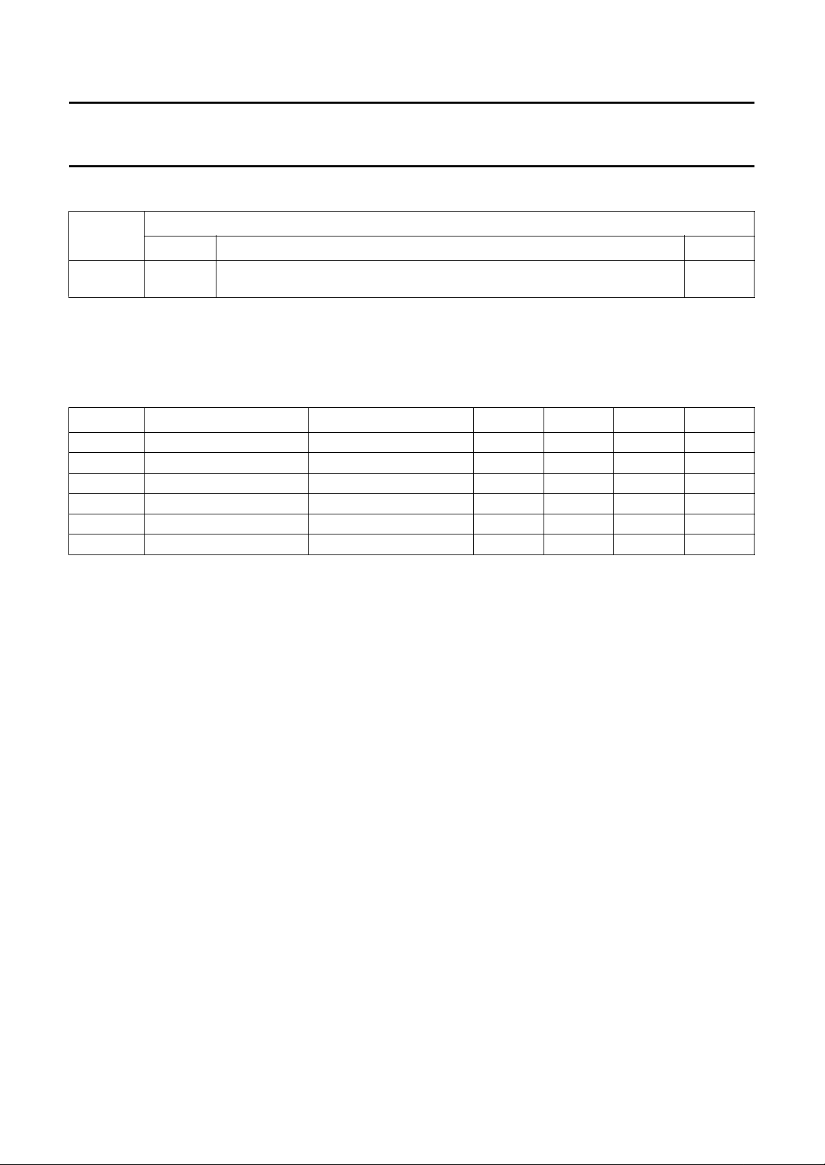
BLOCK DIAGRAM
refTU
refTV
refTY
bias
DAI
DAV
DAV
DAV
DBF
SCL66SDA63POR64A0
book, full pagewidth
SSA
SSD
DAV DAV
SC
WE
RAS
SSD
MV
SSD
SV
SSA
SAV
SSD
SAV
SSA
MAV
SSD
MAV
DDA
DDD
DAV DAV
AD0 to 8
DAI0 to 7
DAO0 to 7
DT
CAS
DDD
MV
DDD
SV
DDA
SAV
DDD
SAV
DDA
MAV
DDD
MAV
18DY14DU16DV19
11 10 20 21
48 to 56
26,25,30,28
41,46,37,34
27 29,31,35,33
47 45 44 32 36,39,40,38
72 73 9 8
82 81 89 90
99 100 92 91
98
MAIN
ACQUISITION
CLAMP AND
A/D CONVERTER
94MY96MV93
13
15
17
AND BUFFER
D/A CONVERTER
MEMORY
CONTROL
SAB9075H
97
95
87
83SY85SV88
24
DISPLAY
SUB
ACQUISITION
CLAMP AND
A/D CONVERTER
86
84
65
7565861
2
I C-BUS
6059
21
3457
79
AND PLL BLOCK
DISPLAY TIMING CONTROL
HUE AND SAT
70
69
67
78
77
76 80
71 23 74
22 42 43
D/A CONVERTERS
68
MBE084
MTCLK
TM2
TM0
SSA
MPV
SSD
MPV
sync
MH
SSA
SPV
bias
SPI
DDD
SPV
sync
SV
SSS
V
DDD
V
VDD
2
I C
STCLK
TC
TM1
DDA
MPV
DDD
MPV
bias
MPI
DDA
SPV
sync
SH
SSD
SPV
sync
MV
Fig.1 Block diagram.
MU
bias
refB
refT
MAI
MAV
MAV
February 1995 4
SU
bias
SAI
refT
SAV
refB
SAV
HUE
SAT
SMUTE
MMUTE
Page 5

Philips Semiconductors Preliminary specification
Picture-in-Picture (PIP) controller for NTSC SAB9075H
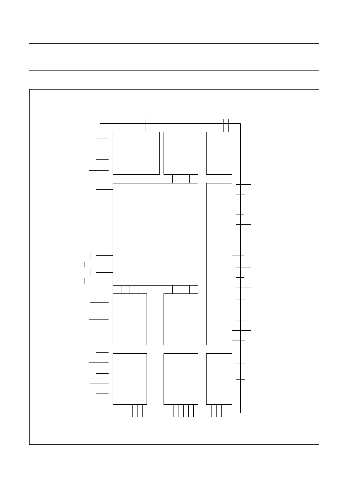
PINNING
SYMBOL PIN I/O TYPE DESCRIPTION
MPV
DDA
MPV
SSA
MH
sync
MPI
bias
MPV
SSD
MTCLK 6 I HPP01 test clock for main-channel
MPV
DDD
MV
DDD
MV
SSD
DAV
DDD
DAV
SSD
n.c. 12 −−not connected
DAV
refTU
DU 14 O E027 analog U output
DAV
refTV
DV 16 O E027 analog V output
DAV
refTY
DY 18 O E027 analog Y output
DAI
bias
DAV
SSA
DAV
DDA
2
CV
I
DD
MV
sync
DBF 24 O SPF20 fast blanking control output signal
DAI5 25 I HPP01 data bus input from memory; bit 5
DAI4 26 I HPP01 data bus input from memory; bit 4
SC 27 O OPF20 memory shift clock
DAI7 28 I HPP01 data bus input from memory; bit 7
DAI0 29 I HPP01 data bus input from memory; bit 0
DAI6 30 I HPP01 data bus input from memory; bit 6
DAI1 31 I HPP01 data bus input from memory; bit 1
DT 32 O OPF20 memory data transfer; active LOW
DAI3 33 I HPP01 data bus input from memory; bit 3
DAO7 34 O OPF20 data bus output to memory; bit 7
DAI2 35 I HPP01 data bus input from memory; bit 2
DAO0 36 O OPF20 data bus output to memory; bit 0
DAO6 37 O OPF20 data bus output to memory; bit 6
DAO3 38 O OPF20 data bus output to memory; bit 3
DAO1 39 O OPF20 data bus output to memory; bit 1
DAO2 40 O OPF20 data bus output to memory; bit 2
1 I/O E030 analog positive power supply for PLL main-channel
2 I/O E009 analog negative power supply for PLL main-channel
3 I E027 horizontal synchronization for main-channel
4 I E027 analog bias reference current for PLL main-channel
5 I/O E009 digital negative power supply for PLL main-channel
7 I/O E030 digital positive power supply for PLL main-channel
8 I/O E030 digital positive power supply for main-channel core
9 I/O E009 digital negative power supply for main-channel core
10 I/O E030 digital positive power supply for DACs
11 I/O E009 digital negative power supply for DACs
13 I/O E027 analog reference voltage for top U DAC
15 I/O E027 analog reference voltage for top V DAC
17 I/O E027 analog reference voltage for top Y DAC
19 I E027 analog bias reference current for DACs
20 I/O E009 analog negative power supply for DACs
21 I/O E030 analog positive power supply for DACs
22 I/O E030 positive supply for HUE and SAT decoders
23 I HPP01 vertical synchronization for main-channel
February 1995 5
Page 6

Philips Semiconductors Preliminary specification
Picture-in-Picture (PIP) controller for NTSC SAB9075H
SYMBOL PIN I/O TYPE DESCRIPTION
DAO4 41 O OPF20 data bus output to memory; bit 4
V
DDD
V
SSS
WE 44 O OPF20 memory write enable; active LOW
CAS 45 O OPF20 memory column address strobe; active LOW
DAO5 46 O OPF20 data bus output to memory; bit 5
RAS 47 O OPF20 memory row address strobe; active LOW
AD0 48 O OPF20 memory address bus; bit 0
AD8 49 O OPF20 memory address bus; bit 8
AD1 50 O OPF20 memory address bus; bit 1
AD6 51 O OPF20 memory address bus; bit 6
AD2 52 O OPF20 memory address bus; bit 2
AD5 53 O OPF20 memory address bus; bit 5
AD3 54 O OPF20 memory address bus; bit 3
AD4 55 O OPF20 memory address bus; bit 4
AD7 56 O OPF20 memory address bus; bit 7
n.c. 57 −−not connected
TC 58 I HPP01 test control
TM0 59 I HPP01 test mode 0
TM1 60 I HPP01 test mode 1
TM2 61 I HPP01 test mode 2
n.c. 62 −−not connected
POR 63 I HUP07 power-on reset
A0 64 I HPF01 I
SCL 65 I HPF01 shift clock for I
SDA 66 I/O IOI41 shift I
MMUTE 67 O SPF20 mute output for main-channel
SMUTE 68 O SPF20 mute output for sub-channel
SAT 69 O E027 analog output for SAT decoder
HUE 70 O E027 analog output for HUE decoder
SV
sync
SV
SSD
SV
DDD
SPV
DDD
STCLK 75 I HPP01 test clock for sub-channel
SPV
SSD
SPI
bias
SH
sync
SPV
SSA
SPV
DDA
SAV
DDD
42 I/O E030 digital positive power supply for peripherals
43 I/O E009 digital negative power supply for peripherals
2
C-bus address 0 selection pin
2
C-bus
2
C-bus input data; acknowledge I2C-bus output data
71 I HPP01 vertical synchronization for sub-channel
72 I/O E009 digital negative power supply for sub-channel core
73 I/O E030 digital positive power supply for sub-channel core
74 I/O E030 digital positive power supply for PLL sub-channel
76 I/O E009 digital negative power supply for PLL sub-channel
77 I E027 analog bias reference current for PLL sub-channel
78 I E027 horizontal synchronization for sub-channel
79 I/O E009 analog negative power supply for PLL sub-channel
80 I/O E030 analog positive power supply for PLL sub-channel
81 I/O E030 digital positive power supply for ADC sub-channel
February 1995 6
Page 7

Philips Semiconductors Preliminary specification
Picture-in-Picture (PIP) controller for NTSC SAB9075H
SYMBOL PIN I/O TYPE DESCRIPTION
SAV
SSD
SU 83 I E027 analog U input for sub-channel
SAV
refB
SV 85 I E027 analog V input for sub-channel
SAV
refT
SY 87 I E027 analog Y input for sub-channel
SAI
bias
SAV
SSA
SAV
DDA
MAV
DDA
MAV
SSA
MAI
bias
MU 94 I E027 analog U input for main-channel
MAV
refB
MV 96 I E027 analog V input for main-channel
MAV
refT
MY 98 I E027 analog Y input for main-channel
MAV
SSD
MAV
DDD
82 I/O E009 digital negative power supply for ADC sub-channel
84 I/O E027 analog reference voltage for bottom ADC sub-channel
86 I/O E027 analog reference voltage for top ADC sub-channel
88 I E027 analog bias reference current for ADC sub-channel
89 I/O E009 analog negative power supply for ADC sub-channel
90 I/O E030 analog positive power supply for ADC sub-channel
91 I/O E030 analog positive power supply for ADC main-channel
92 I/O E009 analog negative power supply for ADC main-channel
93 I E027 analog bias reference current for ADC main-channel
95 I/O E027 analog reference voltage for bottom ADC main-channel
97 I/O E027 analog reference voltage for top ADC main-channel
99 I/O E009 digital negative power supply for ADC main-channel
100 I/O E030 digital positive power supply for ADC main-channel
Table 1 Pin type explanation
PIN TYPE DESCRIPTION
E030 V
E009 VSSpin; diode to V
E027 analog input pin; diode to VDD and V
HPF01 digital input pin; CMOS levels, diode to V
HPP01 digital input pin; CMOS levels, diode to VDD and V
pin; diode to V
DD
SS
DD
SS
SS
SS
HUP07 digital input pin; CMOS levels with hysteresis, pull up resistor to VDD, diode to VDD and V
IOI41 I2C-bus pull-down output stage; CMOS input levels
OPF20 digital output pin
SPF20 digital output pin; slew rate controlled
SS
February 1995 7
Page 8
Philips Semiconductors Preliminary specification
Picture-in-Picture (PIP) controller for NTSC SAB9075H
SSS
DDD
V
DAO4
DAO2
DAO1
DAO3
DAO6
DAO0
DAI2
DAO7
DAI3DTDAI1
32
33
34
35
36
37
38
39
40
41
42
43
44
SAB9075H
MBE083
31
DAI6
30
DAI0
29
DAI7
28
SC
27
DAI4
26
DAI5
25
DBF
24
sync
23
22
21
20
19
18
17
16
15
14
13
12
11
10
9
8
7
6
5
4
3
2
1
DD
DY
DV
DU
n.c.
DDA
SSA
bias
refTY
refTV
refTU
SSD
DDD
SSD
DDD
DDD
SSD
bias
sync
SSA
DDA
MV
I C V
2
DAV
DAV
DAI
DAV
DAV
DAV
DAV
DAV
MV
MV
MPV
MTCLK
MPV
MPI
MH
MPV
MPV
Fig.2 Pin configuration.
sync
SSD
DDD
DDD
SSD
bias
sync
SSA
DDA
AD6
51
AD2
52
53
AD5
54
AD3
AD4
55
AD7
56
57
n.c.
58
TC
TM0
59
TM1
60
61
TM2
62
n.c.
63 POR
64 A0
65
SCL
66 SDA
67 MMUTE
SMUTE
68
69
SAT
70
HUE
71
SV
72
SV
73
SV
74
SPV
75 STCLK
76
SPV
77
SPI
78
SH
79
SPV
80
SPV
50 AD1
AD8
49
AD0
48
RAS
47
DAO5
46
CASWEV
45
90
89
88
87
86
85
84
83
82
81
SY
SV
DDD
SAV
SSD
SAV
SU
refB
SAV
refT
SAV
bias
SAI
SSA
SAV
DDA
SAV
February 1995 8
91
DDA
MAV
92
SSA
MAV
93
bias
MAI
94
MU
95
refB
MAV
96
MV
97
refT
MAV
98
MY
99
SSD
MAV
100
DDD
MAV
Page 9
Philips Semiconductors Preliminary specification
Picture-in-Picture (PIP) controller for NTSC SAB9075H
FUNCTIONAL DESCRIPTION
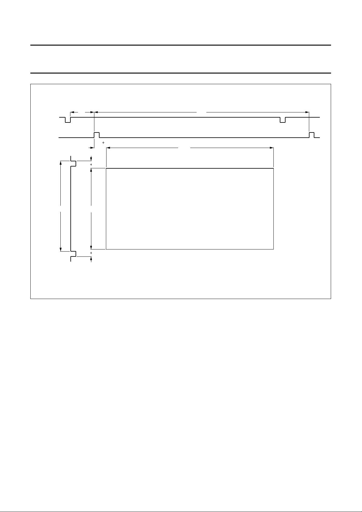
Acquisition area
The acquisition area is in the centre of the visible screen
area. Vertically 228 lines are sampled. Horizontally
672 Y-pixels are processed. The exact active processing
area can be fine tuned in horizontal (2 pixels/steps,
16 steps) and vertical (1 line/step, 16 steps) direction for
both main and sub-channel by the I
2
C-bus (see Fig.3). The
given numbers are pixel numbers at a 13.5 MHz data rate.
The signals, which are dependent on the I2C-bus registers,
can also be related to the H
, in which event they are
sync
delayed by 68 pixels.
Chrominance format
The chrominance format is 4:1:1.
The YUV signals are sampled at a rate of 27 MHz and then
filtered and subsampled to a data rate of 13.5 MHz.
handbook, full pagewidth
clamp
H
sync
32
68
It is expected that the input signals do not contain
frequencies outside the video bandwidth (Y
= 4.5 MHz;
BW
UBWand VBW= 1.125 MHz).
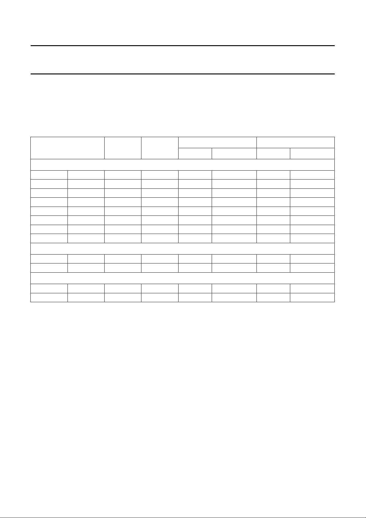
Display area
The display area is shown in Fig.4. The given numbers are
pixels at a data rate of 13.5 MHz. The signals are related
to the burstkey and the V
registers the signals can also be related to the H
. Dependent on the I2C-bus
sync
sync
.
The internal 13.5 MHz data rate is upsampled to the
double frequency (27 MHz) and then fed to the DACs.
2
The display output can be fine positioned by the I
C-bus in
64 steps of 4 pixels in horizontal direction and 64 steps of
1 line/field in vertical direction.
864
burstkey
sync
80 FT
104 FTV
18 FT
228262.5
18 FT
672
624
1/1, 1/3 and 1/4 reduction
1/2 reduction
MBE085
Fig.3 Acquisition area.
February 1995 9
Page 10
Philips Semiconductors Preliminary specification
Picture-in-Picture (PIP) controller for NTSC SAB9075H
handbook, full pagewidth
H
sync
burstkey
V
sync
68 864
36 FT
672
11 FT
228262.5
11 FT
MBE086
Fig.4 Display area.
February 1995 10
Page 11
Philips Semiconductors Preliminary specification
Picture-in-Picture (PIP) controller for NTSC SAB9075H
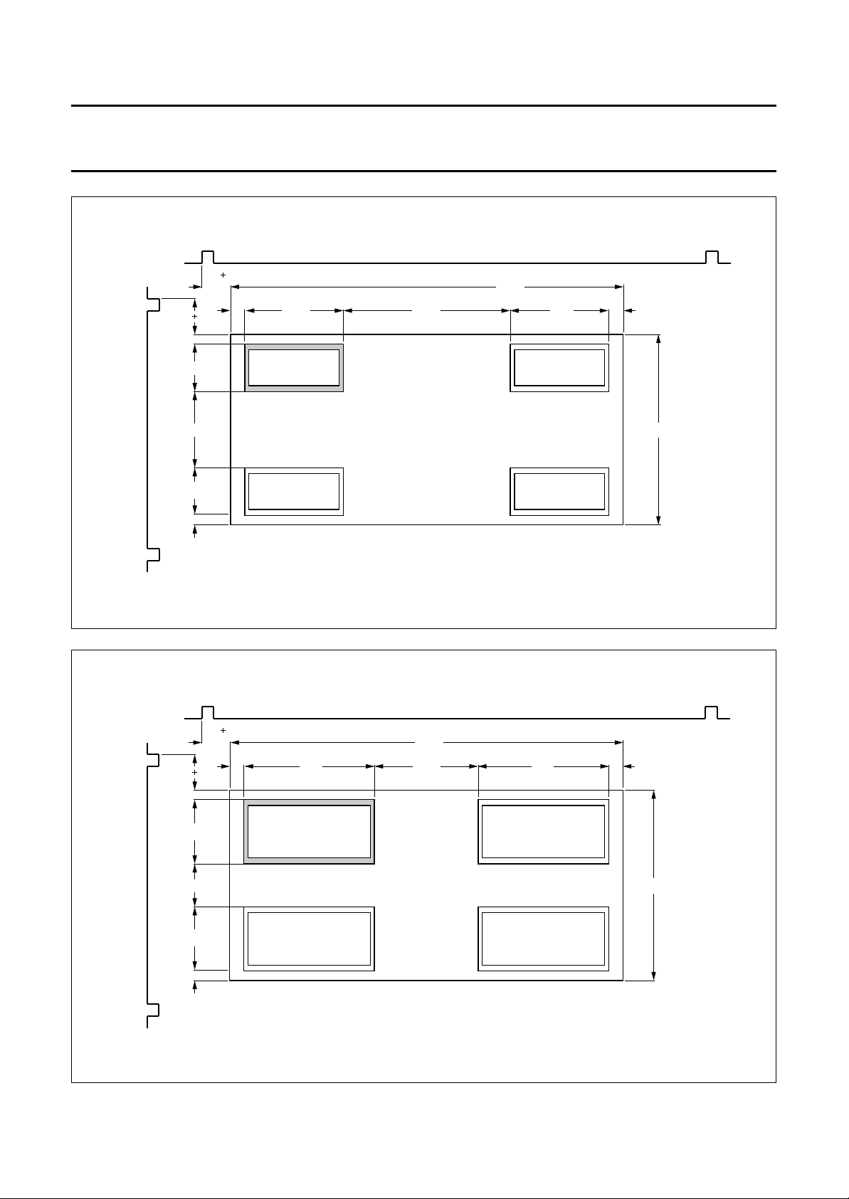
PIP modes
The controller contains two independent acquisition-channels which provide the scaling factors to support the range of
different modes. With the external memory of 2 Mbit it is possible to select between single, double and multi-PIP modes.
Table 2 gives an overview of the different PIP modes.
Table 2 PIP modes
SUB SIZE
(1)
MODE SUB MAIN
PIXELS REDUCTION
4 : 3 main +4:3 subto 4:3screen or 16 : 9 main + 16 : 9 sub to 16 : 9 screen
1
1.1 SPS
1.2 SPL
1.3 DP
⁄
1
⁄
1
⁄
1.4 MP3 3 ×
1.5 MP4 3 ×
1.6 MP7 7 ×
1.7 MP8 7 ×
1.8 MP9 8 ×
16
9
4
1
⁄
16
1
⁄
16
1
⁄
16
1
⁄
16
1
⁄
9
− 160P, 53L1⁄4H,1⁄4V −−
− 216P, 72L1⁄3H,1⁄3V −−
1
⁄
4
304P, 108L1⁄2H,1⁄2V 304P, 108L1⁄2H,1⁄2V
− 160P, 53L1⁄4H,1⁄4V −−
1
⁄
4
160P, 53L1⁄4H,1⁄4V 304P, 108L1⁄2H,1⁄2V
− 160P, 53L1⁄4H,1⁄4V −−
1
⁄
4
1
⁄
9
160P, 53L1⁄4H,1⁄4V 304P, 108L1⁄2H,1⁄2V
216P, 72L1⁄3H,1⁄3V 216P, 72L1⁄3H,1⁄3V
16:9sub+4:3main to 4 : 3 screen
2.1 SPS
2.2 SPL
1
⁄
16
1
⁄
9
− 216P, 53L1⁄3H,1⁄4V −−
− 304P, 72L1⁄2H,1⁄3V −−
4 : 3 sub + 16 : 9 main to 16 : 9 screen
3.1 SPS
3.2 DP
1
⁄
16
1
⁄
4
− 160P, 72L1⁄4H,1⁄3V
1
⁄
4
216P, 108L1⁄3H,1⁄2V 304P, 108L1⁄2H,1⁄2V
MAIN SIZE
(2)
PIXELS REDUCTION
(1)
(2)
Notes
1. The given sub/main sizes are visible PIP sizes, a border is drawn around these PIPs and does not influence these
sizes. The size of the border is 4 pixels wide and 2 lines/fields high.
2. The SAB9075H can be set in automatic mode in which the reduction factors are automatically set by the mode select
and aspect ratio select bits of the I
2
C-bus. If the automatic mode is switched OFF the reduction factors can be set
manually. This will give more flexibility to adjust the aspect ratios of incoming signals.
PIP positions
The positions are graphically depicted in Figs 5 to 17.
February 1995 11
Page 12
Philips Semiconductors Preliminary specification
Picture-in-Picture (PIP) controller for NTSC SAB9075H
handbook, full pagewidth
burstkey
V
sync
11 FT
11
57
92
57
11
36 FT
288
S
Fig.5 Single-PIP, size1⁄16(mode SPS).
672
2416824 168
228
MBE087
handbook, full pagewidth
burstkey
V
sync
11 FT
11
76
54
76
11
36 FT
24
224
176
S
Fig.6 Single-PIP, size1⁄9(mode SPL).
February 1995 12
672
224
24
228
MBE088
Page 13

Philips Semiconductors Preliminary specification
Picture-in-Picture (PIP) controller for NTSC SAB9075H
handbook, full pagewidth
burstkey
V
sync
11 FT
58
112
58
36 FT
672
24
312
312
S M
24
228
MBE089
Fig.7 Double-PIP, size1⁄16(mode DP).
handbook, full pagewidth
burstkey
V
sync
11 FT
24
57
5
57
5
57
23
36 FT
C0
C1
C2
Fig.8 Multi PIP, 3 × sub1⁄16(mode MP3).
February 1995 13
672
264
3616836 168
228
MBE090
Page 14

Philips Semiconductors Preliminary specification
Picture-in-Picture (PIP) controller for NTSC SAB9075H
handbook, full pagewidth
burstkey
V
sync
11 FT
24
57
5
57
5
57
23
36 FT
34
112
35
672
120
C0
C1
M
C2
Fig.9 Multi-PIP, 3 × sub1⁄16, 1 × main1⁄4 (mode MP4).
3631236 168
228
MBE091
handbook, full pagewidth
burstkey
V
sync
11 FT
24
57
5
57
5
57
23
36 FT
34
112
35
672
312 168120
M
Fig.10 Multi-PIP, 3 × sub1⁄16, 1 × main1⁄4 (mode MP4, Right).
February 1995 14
C0
C1
C2
3636
228
MBE092
Page 15

Philips Semiconductors Preliminary specification
Picture-in-Picture (PIP) controller for NTSC SAB9075H
handbook, full pagewidth
burstkey
V
sync
11 FT
57
57
57
57
36 FT
672
168
168 168 168
C0
C1
C2
C3 C4 C5 C6
Fig.11 Multi-PIP, 7 × sub1⁄16, main life (mode MP7).
228
MBE093
handbook, full pagewidth
burstkey
V
sync
11 FT
57
57
57
57
36 FT
168
168 168 168
C0
C1
C2
C3 C4 C5 C6
Fig.12 Multi-PIP, 7 × sub1⁄16, 1 × main1⁄4 (mode MP8).
February 1995 15
672
9696 312
30
M
MBE094
112
228
29
Page 16

Philips Semiconductors Preliminary specification
Picture-in-Picture (PIP) controller for NTSC SAB9075H
handbook, full pagewidth
burstkey
V
sync
36 FT
11 FT
76
76 C3
76
Fig.13 Multi-PIP, 8 × sub1⁄9, 1 × main1⁄9(mode MP9).
224
C0
C5
224
C1
M
C6
672
224
C2
C4
C7
228
MBE095
handbook, full pagewidth
burstkey
V
sync
11 FT
11
76
54
76
11
36 FT
24
168
S
Fig.14 Single-PIP, 4 : 3 sub to 16 : 9 screen (mode SPS).
February 1995 16
288
672
168
24
228
MBE097
Page 17

Philips Semiconductors Preliminary specification
Picture-in-Picture (PIP) controller for NTSC SAB9075H
handbook, full pagewidth
burstkey
V
sync
11 FT
11
57
92
57
11
36 FT
672
176
S
Fig.15 Single-PIP, 16 : 9 sub to 4 : 3 screen (mode SPS).
2422424 224
228
MBE096
handbook, full pagewidth
burstkey
V
sync
11 FT
11
76
54
76
11
36 FT
24
312
S
Fig.16 Single-PIP, 16 : 9 sub to 4 : 3 screen (mode SPL).
February 1995 17
672
312
24
228
MBE098
Page 18

Philips Semiconductors Preliminary specification
Picture-in-Picture (PIP) controller for NTSC SAB9075H
handbook, full pagewidth
burstkey
V
sync
36 FT
696
11 FT
238
MBE099
Fig.17 Factory mode.
February 1995 18
Page 19

Philips Semiconductors Preliminary specification
Picture-in-Picture (PIP) controller for NTSC SAB9075H
2
I
I2C-bus
The I2C-bus provides bi-directional 2-line communication
between different ICs. The SDA line is the Serial Data line
and the SCL serves as Serial Clock Line. Both lines must
be connected to a positive supply via a pull-up resistor
when connected to the output stages of a device. Data
transfer may be initiated only when the bus is not busy.
The SAB9075H has the I2C-bus addresses 2C and 2E,
switchable by the pin A0. Valid subaddresses are
00H to 0FH.
2
Table 3 Overview ofI
SA BIT 7 BIT 6 BIT 5 BIT 4 BIT 3 BIT 2 BIT 1 BIT 0
00 PIPON MANRED MASPECT SASPECT MODE3 MODE2 MODE1 MODE0
01 HPOS VPOS MFREEZE SFREEZE note 2 BCOLPOL MVFILT SVFILT
02 note 2 note 2 DHFP5 DHFP4 DHFP3 DHFP2 DHFP1 DHFP0
03 note 2 note 2 DVFP5 DVFP4 DVFP3 DVFP2 DVFP1 DVFP0
04 MREDH1 MREDH0 MREDV1 MREDV0 SREDH1 SREDH0 SREDV1 SREDV0
05 note 2 CBSEL2 CBSEL1 CBSEL0 note 2 SLSEL2 SLSEL1 SLSEL0
06 note 2 MBON MBBRT1 MBBRT0 note 2 MBCOL2 MBCOL1 MBCOL0
07 note 2 SBON SBBRT1 SBBRT0 note2 SBCOL2 SBCOL1 SBCOL0
08 note 2 CBON CBBRT1 CBBRT0 note 2 CBCOL2 CBCOL1 CBCOL0
09 FACMODE BGON BGBRT1 BGBRT0 note 2 BGCOL2 BGCOL1 BGCOL0
0A MCOLPOL MVSPOL MHSYNC MFPOL SCOLPOL SVSPOL SHSYNC SFPOL
0B MAAHFP3 MAAHFP3 MAAHFP3 MAAHFP3 MAAVFP3 MAAVFP3 MAAVFP3 MAAVFP3
0C SAAHFP3 SAAHFP3 SAAHFP3 SAAHFP3 SAAVFP3 SAAVFP3 SAAVFP3 SAAVFP3
0D note 2 note 2 HUE5 HUE4 HUE3 HUE2 HUE1 HUE0
0E note 2 note 2 SAT5 SAT4 SAT3 SAT2 SAT1 SAT0
0F MMUTE SMUTE note 2 note 2 note 2 note 2 note 2 note 2
C-bus addresses (note 1)
Data Bytes
C-bus control is in accordance with the I2C-bus protocol.
First a start sequence must be put on the I2C-bus, then the
I2C-bus address 2C or 2E, followed by a subaddress
00 to 0F. After this sequence, the data of the subaddress
must be sent. An auto-increment function then gives the
option ‘send data’ of the incremented subaddresses until a
stop sequence has been given.
Notes
1. Table 3 gives an overview of the I2C-bus addresses. They will be explained in more detail in the following pages.
2. Some address spaces are unused but already implemented for future functionality.
February 1995 19
Page 20

Philips Semiconductors Preliminary specification
Picture-in-Picture (PIP) controller for NTSC SAB9075H
Table 4 PIP mode control (note 1)
PIP MODE ASPECT RATIO MAIN-REDUCTION
NAME MODE
(3)
MAIN
(4)
SUB
(4)
HOR VER HOR VER
(2)
SPS 0000 0 0 −−
SPS 0000 0 1 −−
SPS 0000 1 0 −−
SPS 0000 1 1 −−
SPL 0001 0 0 −−
SPL 0001 0 1 −−
SPL 0001 1 X −−
DP 1010 0 X
DP 1010 1 0
DP 1010 1 1
1
⁄
2
1
⁄
2
1
⁄
2
1
⁄
2
1
⁄
2
1
⁄
2
MP3 0110 X X −−
MP4 1110 X X
1
⁄
2
1
⁄
2
MP7 0100 X X −−
MP8 1100 X X
MP9 1001 X X
1
⁄
2
1
⁄
3
1
⁄
2
1
⁄
3
SUB-REDUCTION
1
⁄
4
1
⁄
3
1
⁄
4
1
⁄
4
1
⁄
3
1
⁄
2
1
⁄
3
1
⁄
2
1
⁄
3
1
⁄
2
1
⁄
4
1
⁄
4
1
⁄
4
1
⁄
4
1
⁄
3
(2)
1
⁄
4
1
⁄
4
1
⁄
3
1
⁄
4
1
⁄
3
1
⁄
3
1
⁄
3
1
⁄
2
1
⁄
2
1
⁄
2
1
⁄
4
1
⁄
4
1
⁄
4
1
⁄
4
1
⁄
3
Notes
1. Table 4 gives an overview of the possible PIP modes and how to set them via the I
2
C-bus.
2. The columns main and sub-reduction indicate how the PIP pictures appear on the screen.
3. The column mode corresponds to the lower 4 bits of I2C-bus Register 0.
4. The main and sub-aspect ratios correspond to the bits 5 and 6 of I2C-bus Register 0.
February 1995 20
Page 21

Philips Semiconductors Preliminary specification
Picture-in-Picture (PIP) controller for NTSC SAB9075H
Table 5 Register0; PIP mode control register
BIT MODE RESULT
(1)
7 PIPON logic 0 = PIP function is OFF
6 MANRED logic 0 = automatic reduction factors
(5)
(5)
(5)
(5)
(4)
main-aspect ratio; 0 = 4 : 3; 1 = 16 : 9
(4)
sub-aspect ratio; 0 = 4 : 3; 1 = 16 : 9
PIP mode
PIP mode
PIP mode
PIP mode
5 MASPECT
4 SASPECT
3 MODE(3)
2 MODE(2)
1 MODE(1)
0 MODE(0)
Notes
1. With PIPON in OFF mode the fast blanking signal is made inactive. All other functions will operate as if the circuit
were in operational mode.
2. With MANRED set to logic 0 the reduction factors will be set automatically, dependent on the PIP mode and the
aspect ratio bits of main and sub (bits 5 and 4). Table 4 indicates which bits should be set to obtain a certain PIP
mode.
3. With MANRED set to logic 1 the calculation of the reduction factors is not carried out and should be set by Register 4
(see Table 9). Only combinations with MANRED set to logic 0 are guaranteed.
4. MASPECT and SASPECT are used in automatic mode (MANRED) to indicate the type of input signals, together with
MODE the PIP mode can be set (see Table 4). In manual mode these bits are ignored.
5. The MODE bits set the PIP mode. For the multi-PIP modes the frozen PIPs are set to the 30% grey colour. Once a
PIP has been made live it will always display the last video data.
; logic 1 = PIP function is ON
(2)
; logic 1 = manual reduction factors
(3)
Table 6 Register1; general control register
BIT MODE RESULT
(1)
(1)
logic 0 = left; logic 1 = right
logic 0 = top; logic 1 = bottom
(2)
logic 0 = main-freeze is OFF; logic 1 = main-freeze is ON
(2)
logic 0 = sub-freeze is OFF; logic 1 = sub-freeze is ON
7 HPOS
6 VPOS
5 MFREEZE
4 SFREEZE
3 − not used
(3)
2 BCOLPOL
1 MVFILT
0 SVFILT
(4)
(4)
border UV polarity; logic 0 = +(B−Y), +(R−Y); logic 1 = −(B−Y), −(R−Y)
main-vertical filter mode; logic 0 = Mode 0; logic 1 = Mode 1
sub-vertical filter mode; logic 0 = Mode 0; logic 1 = Mode 1
Notes
1. HPOS and VPOS determine the general location of the sub-PIP on the screen. HPOS only operates in modes SPS,
SPL, DP, MP3 and MP4. VPOS only operates in modes SPS and SPL. The default location of the sub-pictures will
be left top.
2. MFREEZE will freeze the main-picture, and SFREEZE will freeze the sub-picture selected by the live select bits as
in Register 8 (see Table 13).
3. BCOLPOL can invert the border polarity of U and V.
4. MVFILT and SVFILT set the type of vertical filtering for the main and sub-channel. Mode 1 means that diagonal lines
are linearized, in Mode 0 this option is switched OFF. This filtering mode only operates with vertical reduction
1
factors
⁄3 and1⁄4.
February 1995 21
Page 22

Philips Semiconductors Preliminary specification
Picture-in-Picture (PIP) controller for NTSC SAB9075H
Table 7 Register2; display horizontal fine position register
BIT MODE DESCRIPTION
7 − not used
6 − not used
5 DHFP(5) horizontal fine position (64 steps)
4 DHFP(4) horizontal fine position
3 DHFP(3) horizontal fine position
2 DHFP(2) horizontal fine position
1 DHFP(1) horizontal fine position
0 DHFP(0) horizontal fine position
Note
1. The display position can be set in steps of 4 pixels/lines and 1 line/field. The offsets on the display position are
depicted in Fig.4.
Table 8 Register3; display vertical fine position register
BIT MODE DESCRIPTION
7 − not used
6 − not used
5 DVFP(5) vertical fine position (64 steps)
4 DVFP(4) vertical fine position
3 DVFP(3) vertical fine position
2 DVFP(2) vertical fine position
1 DVFP(1) vertical fine position
0 DVFP(0) vertical fine position
(1)
(1)
Note
1. The display position can be set in steps of 4 pixels/lines and 1 line/field. The offsets on the display position are
depicted in Fig.4.
Table 9 Register4; reduction factor register
BIT MODE DESCRIPTION
(1)
7 MREDH(1) main-horizontal reduction factor
6 MREDH(0) main-horizontal reduction factor
5 MREDV(1) main-vertical reduction factor
4 MREDV(0) main-vertical reduction factor
3 SREDH(1) sub-horizontal reduction factor
2 SREDH(2) sub-horizontal reduction factor
1 SREDV(1) sub-vertical reduction factor
0 SREDV(0) sub-vertical reduction factor
Note
1
1. 01 =
⁄1; 10 =1⁄2; 11 =1⁄3; 00 =1⁄4.
February 1995 22
Page 23

Philips Semiconductors Preliminary specification
Picture-in-Picture (PIP) controller for NTSC SAB9075H
Table 10 Register 5; channel select register
BIT MODE DESCRIPTION
7 − not used
(1)
6 CBSEL(2)
5 CBSEL(1)
4 CBSEL(0)
3 − not used
2 SLSEL(2)
1 SLSEL(1)
0 SLSEL(0)
Notes
1. With CBSEL one border of the displayed sub-borders can be selected independently of the SLSEL. This only
operates when the channel select-border is ON as in Register 8 (see Table 13) and when the selected channel
number is displayed.
2. With SLSEL the active sub-live picture can be selected. This only operates when the SFREEZE is OFF as in
Register 1 (see Table 6) and when the selected channel is displayed.
channel-border select (maximum 8 channels)
(1)
channel-border select
(1)
channel-border select
(2)
sub-live select (maximum 8 channels)
(2)
sub-live select
(2)
sub-live select
Background and main, sub and channel-border
colour and brightness handling
Registers 6 to 9 (see Tables 11 to 14) handle background
and main, sub and channel-border colour and brightness.
The borders and background can be set ON and OFF.
Background, main and sub-borders are black when they
are OFF. The channel-border gets the current sub-border
colour when it is switched OFF. The brightness can be set
in 4 steps (30%, 50%, 70% and 100%). Eight different
colours can be set in accordance with Table 15.
Table 11 Register 6; main-border control register
BIT MODE DESCRIPTION
7 − not used
6 MB0N logic 0 = MB is OFF; logic 1 =MB is ON
5 MBBRT(1) main-border brightness (4 steps)
4 MBBRT(0) main-border brightness
3 − not used
2 MBCOL(2) main-border colour (8 colours)
1 MBCOL(1) main-border colour
0 MBCOL(0) main-border colour
February 1995 23
Page 24

Philips Semiconductors Preliminary specification
Picture-in-Picture (PIP) controller for NTSC SAB9075H
Table 12 Register 7; sub-border control register
BIT MODE DESCRIPTION
7 − not used
6 SBON logic 0 = SB is OFF; logic 1 = SB is ON
5 SBBRT(1) sub-border brightness (4 steps)
4 SBBRT(0) sub-border brightness
3 − not used
2 SBCOL(2) sub-border colour (8 colours)
1 SBCOL(1) sub-border colour
0 SBCOL(0) sub-border colour
Table 13 Register 8; channel-border control register
BIT MODE DESCRIPTION
7 − not used
6 CBON logic 0 = CB is OFF; logic 1 = CB is ON
5 CBBRT(1) channel-border brightness (4 steps)
4 CBBRT(0) channel-border brightness
3 − not used
2 CBCOL(2) channel-border colour (8 colours)
1 CBCOL(1) channel-border colour
0 CBCOL(0) channel-border colour
Table 14 Register 9; background control register
BIT MODE DESCRIPTION
(1)
7 FACMODE
6 BGON logic 0 = BG is OFF; logic 1 = BG is ON
5 BGBRT(1) background brightness (4 steps)
4 BGBRT(0) background brightness
3 − not used
2 BGCOL(2) background colour (8 colours)
1 BGCOL(1) background colour
0 BGCOL(0) background colour
Note
1. The FACMODE bit controls the factory mode which shows an enlarged background colour as depicted in Fig.17
(BGON must be set).
logic 0 = FM is OFF; logic 1 = FM is ON
February 1995 24
Page 25

Philips Semiconductors Preliminary specification
Picture-in-Picture (PIP) controller for NTSC SAB9075H
Table 15 Colour table
COLOUR TYPE
BRIGHTNESS (%)
0 103050607080100
Black/white 40H 50H 60H 70H 47H 57H 67H 77H
Blue −−41H 51H − 61H − 71H
Red −−42H 52H − 62H − 72H
Magenta −−43H 53H − 63H − 73H
Green −−44H 54H − 64H − 74H
Cyan −−45H 55H − 65H − 75H
Yellow −−46H 56H − 66H − 76H
Note
1. The values in are the I
2
C-bus register values for the Colour Control Registers 6 to 9 (see Tables 11 to 14). The
values are hexadecimal values of which the left part indicates the brightness and the right part the colour value.
(1)
Table 16 Border display
PIP
MODES
MP4
MP8
MP9
FFS
SPS
SPL
DP
MBON BGON
(1)
SBON CBON
OFF OFF −−live BG
OFF ON −−BGCOL BGCOL −−
ON OFF −−MBCOL live BG
ON ON −−MBCOL BGCOL −−
−−OFF −− −live BG
−−ON −− −SBCOL −
OFF OFF OFF − live BG
OFF ON OFF − BGCOL BGCOL BGCOL −
ON OFF ON − MBCOL live BG
MAIN-
BORDER
DISPLAY
(2)
(3)
(3)
ON ON ON − MBCOL BGCOL SBCOL −
MP3
MP4
MP7
MP8
MP9
− OFF OFF ON − live BG
− ON OFF ON − BGCOL BGCOL CBCOL
− OFF ON ON − live BG
− ON ON ON − BGCOL SBCOL CBCOL
Notes
2
1. The BGON I
C-bus bit controls the display area outside the PIP and border area, set to ON means that the
background gets the BGCOL colour value.
2. The main and sub-border displays are dependent on the I2C-bus switches.
3. ‘Live BG’ means that the original picture is shown.
BACK-
GROUND
DISPLAY
live BG
live BG
(3)
(3)
(3)
(3)
(3)
(3)
SUB-
BORDER
DISPLAY
CHANNEL
BORDER
(2)
DISPLAY
−−
−−
live BG
(3)
(3)
−
−
SBCOL −
live BG
(3)
CBCOL
SBCOL CBCOL
February 1995 25
Page 26

Philips Semiconductors Preliminary specification
Picture-in-Picture (PIP) controller for NTSC SAB9075H
Table 17 Register A; decoder format register
BIT MODE RESULT
(1)
7 MCOLPOL
6 MVSPOL
(2)
5 MHSYNC
4 MFPOL main-field polarity; inverts field identification window
3 SCOLPOL
2 SVSPOL
1 SHSYNC
(2)
(3)
0 SFPOL sub-field polarity, inverts field identification window
Notes
1. MCOLPOL and SCOPOL invert the UV video data.
2. MVSPOL and SVSPOL determine the active edge of the V
be taken; if VSPOL is logic 1, the negative edge of the V
3. MHSYNC and SHSYNC determine whether the H
synchronization.
main-UV polarity; logic 0 = original; logic 1 = inverted
main-vertical sync polarity; logic 0 = positive pulse; logic 1 = negative pulse
(3)
main-horizontal sync selection; logic 0 = burst edge; logic 1 = H − sync
(1)
sub-UV polarity; logic 0 = original; logic 1 = inverted
sub-vertical sync polarity; logic 0 = positive pulse; logic 1 = negative pulse
sub-horizontal sync selection; logic 0 = burst edge; logic 1 = H − sync
. If VSPOL is logic 0, the positive edge of the V
sync
will be taken.
sync
signal or the burstkey is used as internal horizontal
sync
sync
will
The exact timing of the V
in relation to the H
sync
sync
reference pulse is depicted in Fig.18. A field identification
window determines whether a V
is being handled as a
sync
1st field or a 2nd field. This field identification window can
be inverted by the FPOL bit. If FPOL is logic 0 and an
handbook, full pagewidth
H (external)
sync
field ID (internal)
(number of pixels)
V (external)
sync
V (external)
sync
2nd field
Fig.18 V
timing and field identification.
sync
active edge of the V
occurs when the F-ID signal is
sync
logic 0, it will be regarded as the 1st field. If FPOL is logic 0
and an active edge of the V
occurs when the F-ID
sync
signal is logic 1, it will be regarded as the 2nd field. If FPOL
is logic 1 the 1st and 2nd field IDs are changed over.
43238943
1st field
MBE100
February 1995 26
Page 27

Philips Semiconductors Preliminary specification
Picture-in-Picture (PIP) controller for NTSC SAB9075H
Table 18 Register B; main-acquisition area fine position
BIT MODE DESCRIPTION
7 MAAHFP(3) main-acquisition area horizontal fine position
6 MAAHFP(2) main-acquisition area horizontal fine position
5 MAAHFP(1) main-acquisition area horizontal fine position
4 MAAHFP(0) main-acquisition area horizontal fine position
(2)
3 MAAVFP(3)
2 MAAVFP(2)
1 MAAVFP(1)
0 MAAVFP(0)
main-acquisition area vertical fine position
(2)
main-acquisition area vertical fine position
(2)
main-acquisition area vertical fine position
(2)
main-acquisition area vertical fine position
Notes
1. The acquisition area can be adjusted in 16 steps of 2 pixels horizontally and 1 line/field vertically.
2. With MAAVFP a complete field must have been processed before the next V
non-standard signals.
(1)
occurs. This is relevant for
sync
Table 19 Register C; sub-acquisition area fine position
BIT MODE DESCRIPTION
(1)
7 SAAHFP(3) sub-acquisition area horizontal fine position
6 SAAHFP(2) sub-acquisition area horizontal fine position
5 SAAHFP(1) sub-acquisition area horizontal fine position
4 SAAHFP(0) sub-acquisition area horizontal fine position
(2)
3 SAAVFP(3)
2 SAAVFP(2)
1 SAAVFP(1)
0 SAAVFP(0)
sub-acquisition area vertical fine position
(2)
sub-acquisition area vertical fine position
(2)
sub-acquisition area vertical fine position
(2)
sub-acquisition area vertical fine position
Notes
1. The acquisition area can be adjusted in 16 steps of 2 pixels horizontally and 1 line/field vertically.
2. With SAAVFP a complete field must have been processed before the next V
occurs. This is relevant for
sync
non-standard signals.
February 1995 27
Page 28

Philips Semiconductors Preliminary specification
Picture-in-Picture (PIP) controller for NTSC SAB9075H
Auxiliary registers
The Auxiliary Registers D to F (see Tables 20 to 22) are implemented to generate I2C-bus controlled signals for circuits
which do not have an on-board I2C-bus.
Table 20 Register D; Auxiliary Control Register 1
BIT MODE DESCRIPTION
7 − not used
6 − not used
5 HUE(5) hue control (output pin HUE)
4 HUE(4) hue control
3 HUE(3) hue control
2 HUE(2) hue control
1 HUE(1) hue control
0 HUE(0) hue control
Table 21 Register E; Auxiliary Control Register 2
BIT MODE DESCRIPTION
7 − not used
6 − not used
5 SAT(5) saturation control (output pin SAT)
4 SAT(4) saturation control
3 SAT(3) saturation control
2 SAT(2) saturation control
1 SAT(1) saturation control
0 SAT(0) saturation control
Table 22 Register F; Auxiliary Control Register 3
BIT MODE DESCRIPTION
7 MMUTE data bit directly to output pin MMUTE
6 SMUTE data bit directly to output pin SMUTE
5 − not used
4 − not used
3 − not used
2 − not used
1 − not used
0 − not used
February 1995 28
Page 29

Philips Semiconductors Preliminary specification
Picture-in-Picture (PIP) controller for NTSC SAB9075H
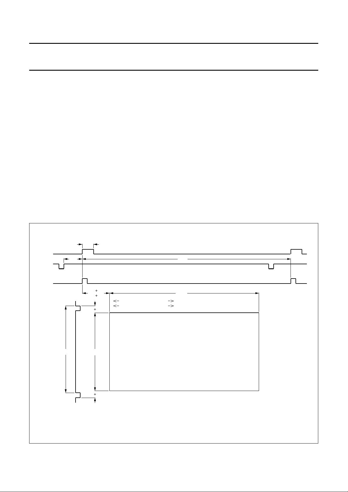
External memory
For the external memory two VDRAMS of type Mitsubishi
M5442256 are used. They have a storage capacity of
262144 words of 4-bit each and will be used in parallel.
An overview of the timing to the VDRAM is depicted in
Fig.19. Three different timing modes are shown. If the
SAB9075 is not in one of these three modes, it is in idle
mode in which all the control signals are HIGH. An idle
mode takes at least 4 clock periods. Switching from one
mode to another is always carried out via this idle mode.
The clock signal shown is an internal clock derived from
the PLLs and is approximately 27 MHz.
Main and sub-ADCs
Both main and sub-channels convert the analog input
signals to digital signals by three ADCs for each channel.
The input levels of the ADCs are equal and can set by the
MAV
refT
, SAV
refT
, MAV
, and SAV
refB
refB
pins.The
reference levels are made internally by a resistor network
which divides the analog VDD to a default set of preferred
signal levels of 1.5 V. If the application requires a different
set of levels the internal resistors can be shunted. External
capacitors are required to filter AC components on the
reference levels.
The resolution of the ADCs is 6-bit and the sampling is
carried out at the system frequency of 27 MHz. The
bias current I
is made internally but can be increased or
bias
decreased.
Output DACs
The digital processed signals are converted to analog
signals by means of three DACs. The output voltages of
these DACs are default set by the DAV
DAV
pins for the TOP-levels. Default signal levels are
refTY
refTU
, DAV
refTV
and
1.5 V. The output buffer after each DAC is a PMOS source
follower.
For more information see chapter “Test and application
information”.
HUE and SAT DACs
The HUE and SAT DACs are resistor DACs based on a
R2R network. They have a direct control from their I
2
C-bus
register and therefore their sample frequency is limited by
the I2C-bus frequency. The output voltage is linear with the
I2CVDD. Therefore the VDD of this block is a separate pin.
PLLs and clock generation
The SAB9075H has two PLLs on-board, one for the subchannel and one for the main-channel and the display part.
The PLLs lock to the input signals MH
sync
and SH
sync
. The
internal clock frequency is 1728 times higher which is
approximately 27 MHz in a standard NTSC system.
The positive edges of the H
signals are the driving
sync
timing points. For good short term stability they have to be
noise/jitter free.
The inputs should be AC-coupled and an internal clamping
circuit will clamp the input to MAV
and SAV
refB
refB
for the
luminance channels and to
MAV
---------------------------------------------------- -
SAV
-------------------------------------------------- -
refT
refT
+
2
+
2
MAV
SAV
refB
refB
+
+
LSB
----------- 2
LSB
----------- 2
for the chrominance channels. The clamping starts at the
active edge of the burstkey.
For more information see chapter “Test and application
information”.
February 1995 29
Page 30

Philips Semiconductors Preliminary specification
Picture-in-Picture (PIP) controller for NTSC SAB9075H
handbook, full pagewidth
CLOCK
RAS
CAS
CLOCK
RAS
CAS
AD0 to AD8
WE
DAI0 to DAI7
refresh cycle
ROW COLUMN COLUMN COLUMN COLUMN COLUMN
write cycle (SUB or MAIN)
CLOCK
RAS
CAS
AD0 to AD8
WE
DT
SC
DAO0 to DAO7
ROW COLUMN
read cycle
Fig.19 VDRAM timing.
SC cycles
MBE101
February 1995 30
Page 31

Philips Semiconductors Preliminary specification
Picture-in-Picture (PIP) controller for NTSC SAB9075H
LIMITING VALUES
In accordance with the Absolute Maximum Rating System (IEC 134)
SYMBOL PARAMETER MIN. MAX. UNIT
V
DD
∆V
DD
T
stg
T
amb
V
esd
P
tot
THERMAL CHARACTERISTICS
SYMBOL PARAMETER VALUE UNIT
R
thj-a
supply voltage −0.5 +6.5 V
supply voltage variation − 0.2 V
storage temperature −25 +150 °C
operating ambient temperature 0 70 °C
electrostatic discharge handling −−V
total power dissipation − 1.5 W
thermal resistance from junction to ambient in free air 38 K/W
QUALITY SPECIFICATION
In accordance with SNW-FQ-611, Part E, dated 14 December 1992.
February 1995 31
Page 32

Philips Semiconductors Preliminary specification
Picture-in-Picture (PIP) controller for NTSC SAB9075H
CHARACTERISTICS
V
= 5.0 V; T
DD
SYMBOL PARAMETER CONDITIONS MIN. TYP. MAX. UNIT
Supplies
V
DD
V
SS
∆V
DD
∆V
SS
I
DDQ
MPIV
DDA
SPIV
DDA
MAIV
DDA
SAIV
DDA
DIV
DDA
2
CV
I
DD
I
tot
Converter and clamping
AV
refT
AV
refB
Rin
ref
V
I
V
i
R
i
R
iY
R
iV
R
iU
C
i
Res resolution − 6 − bit
f
s
DNL differential non-linearity −1.0 − +1.0 LSB
INL integral non-linearity −1.0 − +1.0 LSB
V
os
α
cs
PSRR power supply rejection ratio tbf 40 − dB
=25°C; unless otherwise specified.
amb
positive supply voltage 4.5 5.0 5.5 V
negative supply voltage − 0 − V
maximum voltage difference between
− 0 100 mV
all positive supply pins
maximum voltage difference between
− 0 100 mV
all negative supply pins
quiescent current digital positive
note 1 − 2 tbf µA
supply pins
supply current PLL main − 2.5 tbf mA
supply current PLL sub − 2.5 tbf mA
supply current 3 main-ADCs − 36 tbf mA
supply current 3 sub-ADCs − 36 tbf mA
supply current 3 display DACs − 18 tbf mA
supply current HUE and SAT DACs note 2 − 2.5 5 mA
total supply current tbf 220 tbf mA
top reference voltage note 3 1.0 1.9 2.0 V
bottom reference voltage note 3 0 0.4 1.0 V
input resistance V
DC input voltage V
refT
to V
refB
note 3; 1 ADC tbf 860 tbf Ω
refB
− V
refT
V
AC input voltage (peak-to-peak value) 1.0 1.5 − V
input resistance clamping OFF 1 −−MΩ
input resistance for Y channel clamping ON − 200 −Ω
input resistance for V channel clamping ON − 800 −Ω
input resistance for U channel clamping ON − 800 −Ω
input capacitance − 15 − pF
sample frequency rate note4 − 27 − MHz
input offset voltage −1.0 − +1.0 LSB
channel separation within channel tbf 40 − dB
to other channel tbf 40 − dB
February 1995 32
Page 33

Philips Semiconductors Preliminary specification
Picture-in-Picture (PIP) controller for NTSC SAB9075H
SYMBOL PARAMETER CONDITIONS MIN. TYP. MAX. UNIT
TD
clamp
T
clamp
V
clampY
V
clampU
V
clampV
Digital-to-analog converter
V
refT
Rin
ref
V
o(max)
R
L(min)
C
L(max)
Res resolution − 7 − bit
f
s
DNL differential non-linearity −0.5 − +0.5 LSB
INL integral non-linearity −1.0 − +1.0 LSB
α
cs
PSRR power supply rejection ratio tbf 40 − dB
delay burstkey edge to clamping start − 0 −µs
duration of clamping − 2.33 −µs
clamping voltage level Y AD
clamping voltage level U AD
clamping voltage level V AD
=0H − V
out
= 20H −
out
= 20H − 0.5 V
out
s
0.5 V
− V
− V
T+B
− V
T+B
top reference voltage (Y, U and V) note 3 1.0 1.5 2.0 V
input resistance V
maximum output voltage V
refT
to V
refB
note 3; 1 DAC tbf 1.0 tbf kΩ
refB
− V
refT
V
minimum load resistance 10 −−kΩ
maximum load capacitance − 50 − pF
sample frequency rate note4 − 27 − MHz
channel separation tbf 40 − dB
Digital-to-analog converter HUE/SAT
V
o
R
L(min)
C
L(max)
output voltage V
SS
− V
DD
V
minimum load resistance note 2 100 −−kΩ
maximum load capacitance − 50 − pF
Res resolution − 6 − bit
DNL differential non-linearity −1.0 − +1.0 LSB
INL integral non-linearity −1.0 − +1.0 LSB
PSRR power supply rejection ratio note 2 − 0 − dB
PLL and clock generation; note 4
V
V
V
f
PLL
TOP
LOW
slice
TOP-level input voltage 2.5 − PV
LOW-level input voltage −−0.5 V
slicing voltage level below TOP 0.45 1.0 2.0 V
input frequency 14750 15734 17250 Hz
DD
V
Notes
1. Digital clocks are silent and analog bias current is zero.
2. The HUE and SAT DACs are based on a R2R ladder network as describe in the section “HUE and SAT DACs”. The
maximum output sample frequency is determined by the I2C-bus.
3. The input configuration of the ADCs is depicted in Fig.20. The minimum difference AV
refT
− AV
should be larger
refB
than 1.0 V. The reference voltages can be calculated as follows:
1.9
V
refT
× V= V
AV
DD
------- -
5.0
;
refB
AV
DD
0.4
× V=
------- -
5.0
4. The internal system frequencies are 1728 times the input frequency. For more detailed information about the clock
generation see section “PLLs and clock generation”.
February 1995 33
Page 34

Philips Semiconductors Preliminary specification
Picture-in-Picture (PIP) controller for NTSC SAB9075H
DC CHARACTERISTICS FOR DIGITAL PART
All V
SYMBOL PARAMETER CONDITIONS MIN. TYP. MAX. UNIT
V
V
V
V
V
I
I
R
pins = 4.5 to 5.5 V; T
DD
IH
IL
hys
OH
OL
LI
LOZ
HIGH level input voltage HPF01 70 −−%V
LOW level input voltage IOI41 70 −−%V
hysteresis voltage HUP07 − 33 − %V
HIGH level output voltage OPF20; IOL= −2 mA; VDD= 4.5 V 4.4 −−V
LOW level output voltage IOI41; IOL= +2 mA; VDD= 4.5 V −−0.15 V
input leakage current HPF01 − 0.1 1 µA
three-state output leakage
current
pu
internal pull up resistor HUP07 17 − 134 kΩ
= −20 to +75 °C; unless otherwise specified.
amb
HPP01 70 −−%V
HUP07 80 −−%V
HPF01 −−30 %V
HPP01 −−30 %V
HUP07 −−20 %V
IOI41 −−30 %V
SPF20; I
OPF20; I
SPF20; I
= −2 mA; VDD= 4.5 V 4.4 −−V
OL
= +2 mA; VDD= 4.5 V −−0.15 V
OL
= +2 mA; VDD= 4.5 V −−0.15 V
OL
HPP01 − 0.1 1 µA
IOI41; VDD= 5.5 V − 0.2 5.0 µA
DD
DD
DD
DD
DD
DD
DD
DD
DD
AC CHARACTERISTICS FOR DIGITAL PART
V
= 4.5 5.5 V; T
DD
= −20 to +75 °C; unless otherwise specified.
amb
SYMBOL PARAMETER CONDITIONS MIN. TYP. MAX. UNIT
f
sys
t
r
t
f
system frequency note 1 − 27 30 MHz
rise time VDD= 4.5 V − 625ns
fall time VDD= 4.5 V − 625ns
Note
1. The internal system frequencies are 1728 times the input frequency. For more detailed information about the clock
generation see section “PLLs and clock generation”.
February 1995 34
Page 35

Philips Semiconductors Preliminary specification
Picture-in-Picture (PIP) controller for NTSC SAB9075H
TEST AND APPLICATION INFORMATION
Fig.20 shows how the ADCs and the DACs can be
connected in the application.
The generation of the reference voltages is carried out
internally and they have to be externally decoupled for AC
signals.
For all ADCs and DACs the internal resistor division is
such that a maximum signal voltage level of 1.5 V is
obtained. For the ADCs there is a DC offset voltage of
0.4 V.
handbook, full pagewidth
MAV
MAV
DDA
refT
MY
MU
R
top
ADC
ADC
A modification of these reference voltages can be
achieved by external shunting.
The ADC reference voltages are the same for all Y/U/V
channels which means that their input levels need to be
the same. The DAC voltage references can be set
separately for Y/U/V channels. These reference voltages
can be modified by shunting.
The output buffers of the DACS are PMOS source
followers with a minimum output load of 10 kΩ.
DAV
DAV
DAV
DAV
DDA
refTY
refTU
refTV
3R
top
MAV
MAV
SAV
SAV
SAV
SAV
MV
refB
SSA
DDA
refT
SY
SU
SV
refB
SSA
ADC
R
R
top
ADC
ADC
ADC
R
bottom
bottom
VIDEO
SIGNAL
PROCESSING
DAC
DAC
DAC
MGC001
Fig.20 Analog application diagram ADCs and DACs.
DY
DU
DV
DAV
SSA
February 1995 35
Page 36

Philips Semiconductors Preliminary specification
Picture-in-Picture (PIP) controller for NTSC SAB9075H
handbook, full pagewidth
TMS44C250 TMS44C250
5 V
5 V
5 V
5 V
5 V
MPI
MPV
MPV
MPV
MPV
SPI
SPV
SPV
SPV
SPV
SAV
SAV
bias
DDA
SSA
DDD
SSD
bias
DDA
SSA
DDD
SSD
DDD
SSD
94444
5 V
SSS
DDD
V
V
AD0 to AD8
SSA
DDA
bias
SAI
SAV
SAV
5 V
DAI4 to DAI7
DAO4 to DAO7
SAV
DAI0 to DAI3
DAO0 to DAO3
refT
refB
sync
SAV
SV
SH
sync
SC
SY
CAS
SU
WE
RAS
SAB9075H
SV
HUE
DT
SAT
2
STCLK
MTCLK
DD
SMUTE
I CV
5 V
mute output
main-channel
TC
TM0
MY
MMUTE
mute output
sub-channel
TM1
TM2
MU
5 V
DDD
SV
MV
SSD
SV
sync
MH
5 V
DDD
MV
sync
MV
0 V or 5 V
SSD
POR
MV
refB
refT
MAV
MAV
A0
SSA
MAV
SCL
DAV
DAV
DAV
DDA
MAV
5 V
SDA
DAI
DAV
DAV
DAV
DAV
MAV
MAV
bias
MAI
bias
DDA
SSA
refTY
refTU
refTV
DBF
DY
DU
DV
DDD
SSD
DDD
SSD
MGC053
SCL
SDA
5 V
fast blanking
control output
analog Y output
analog U output
analog V output
5 V
5 V
Y
U
V
SAT
VOUT
HOUT
HUE
TDA8315T
CVBS/Y sub-channel input CVBS/Y main-channel input
Fig.21 Application diagram.
February 1995 36
SAT
HUE
Y U V
TDA8315T
CVBS/Y CVBS/Y
VOUT
HOUT
Page 37

Philips Semiconductors Preliminary specification
Picture-in-Picture (PIP) controller for NTSC SAB9075H
PACKAGE OUTLINE
QFP100: plastic quad flat package; 100 leads (lead length 1.95 mm); body 14 x 20 x 2.8 mm
c
y
X
E
e
w M
p
A
A
H
E
E
2
A
A
1
80 51
81
pin 1 index
100
1
50
Z
b
31
30
detail X
Q
L
p
L
SOT317-2
(A )
3
θ
w M
b
e
p
Z
D
D
H
D
0 5 10 mm
scale
DIMENSIONS (mm are the original dimensions)
mm
A
max.
3.20
0.25
0.05
2.90
2.65
0.25
UNIT A1A2A3b
cE
p
0.40
0.25
0.25
0.14
(1)
(1) (1)(1)
D
20.1
19.9
eH
14.1
13.9
0.65
24.2
23.6
Note
1. Plastic or metal protrusions of 0.25 mm maximum per side are not included.
OUTLINE
VERSION
IEC JEDEC EIAJ
REFERENCES
SOT317-2
February 1995 37
H
D
v M
A
B
v M
B
LLpQZywv θ
E
18.2
17.6
1.0
0.6
1.4
1.2
0.15 0.10.21.95
EUROPEAN
PROJECTION
Z
D
0.8
1.0
0.4
0.6
ISSUE DATE
E
o
7
o
0
92-11-17
95-02-04
Page 38

Philips Semiconductors Preliminary specification
Picture-in-Picture (PIP) controller for NTSC SAB9075H
SOLDERING
Plastic quad flat-packs
YWAVE
B
During placement and before soldering, the component
must be fixed with a droplet of adhesive. After curing the
adhesive, the component can be soldered. The adhesive
can be applied by screen printing, pin transfer or syringe
dispensing.
Maximum permissible solder temperature is 260 °C, and
maximum duration of package immersion in solder bath is
10 s, if allowed to cool to less than 150 °C within 6 s.
Typical dwell time is 4 s at 250 °C.
A modified wave soldering technique is recommended
using two solder waves (dual-wave), in which a turbulent
wave with high upward pressure is followed by a smooth
laminar wave. Using a mildly-activated flux eliminates the
need for removal of corrosive residues in most
applications.
Y SOLDER PASTE REFLOW
B
Reflow soldering requires the solder paste (a suspension
of fine solder particles, flux and binding agent) to be
applied to the substrate by screen printing, stencilling or
pressure-syringe dispensing before device placement.
Several techniques exist for reflowing; for example,
thermal conduction by heated belt, infrared, and
vapour-phase reflow. Dwell times vary between 50 and
300 s according to method. Typical reflow temperatures
range from 215 to 250 °C.
Preheating is necessary to dry the paste and evaporate
the binding agent. Preheating duration: 45 min at 45 °C.
EPAIRING SOLDERED JOINTS (BY HAND-HELD SOLDERING
R
IRON OR PULSE
-HEATED SOLDER TOOL)
Fix the component by first soldering two, diagonally
opposite, end pins. Apply the heating tool to the flat part of
the pin only. Contact time must be limited to 10 s at up to
300 °C. When using proper tools, all other pins can be
soldered in one operation within 2 to 5 s at between 270
and 320 °C. (Pulse-heated soldering is not recommended
for SO packages.)
For pulse-heated solder tool (resistance) soldering of VSO
packages, solder is applied to the substrate by dipping or
by an extra thick tin/lead plating before package
placement.
DEFINITIONS
Data sheet status
Objective specification This data sheet contains target or goal specifications for product development.
Preliminary specification This data sheet contains preliminary data; supplementary data may be published later.
Product specification This data sheet contains final product specifications.
Limiting values
Limiting values given are in accordance with the Absolute Maximum Rating System (IEC 134). Stress above one or
more of the limiting values may cause permanent damage to the device. These are stress ratings only and operation
of the device at these or at any other conditions above those given in the Characteristics sections of the specification
is not implied. Exposure to limiting values for extended periods may affect device reliability.
Application information
Where application information is given, it is advisory and does not form part of the specification.
LIFE SUPPORT APPLICATIONS
These products are not designed for use in life support appliances, devices, or systems where malfunction of these
products can reasonably be expected to result in personal injury. Philips customers using or selling these products for
use in such applications do so at their own risk and agree to fully indemnify Philips for any damages resulting from such
improper use or sale.
February 1995 38
Page 39

Philips Semiconductors Preliminary specification
Picture-in-Picture (PIP) controller for NTSC SAB9075H
NOTES
February 1995 39
Page 40

Philips Semiconductors – a worldwide company
Argentina: IEROD, Av. Juramento 1992 - 14.b, (1428)
BUENOS AIRES, Tel. (541)786 7633, Fax. (541)786 9367
Australia: 34 Waterloo Road, NORTH RYDE, NSW 2113,
Tel. (02)805 4455, Fax. (02)805 4466
Austria: Triester Str. 64, A-1101 WIEN, P.O. Box 213,
Tel. (01)60 101-1236, Fax. (01)60 101-1211
Belgium: Postbus 90050, 5600 PB EINDHOVEN, The Netherlands,
Tel. (31)40 783 749, Fax. (31)40 788 399
Brazil: Rua do Rocio 220 - 5
CEP: 04552-903-SÃO PAULO-SP, Brazil.
P.O. Box 7383 (01064-970).
Tel. (011)821-2333, Fax. (011)829-1849
Canada: PHILIPS SEMICONDUCTORS/COMPONENTS:
Tel. (800) 234-7381, Fax. (708) 296-8556
Chile: Av. Santa Maria 0760, SANTIAGO,
Tel. (02)773 816, Fax. (02)777 6730
Colombia: IPRELENSO LTDA, Carrera 21 No. 56-17,
77621 BOGOTA, Tel. (571)249 7624/(571)217 4609,
Fax. (571)217 4549
Denmark: Prags Boulevard 80, PB 1919, DK-2300 COPENHAGEN S,
Tel. (032)88 2636, Fax. (031)57 1949
Finland: Sinikalliontie 3, FIN-02630 ESPOO,
Tel. (9)0-50261, Fax. (9)0-520971
France: 4 Rue du Port-aux-Vins, BP317,
92156 SURESNES Cedex,
Tel. (01)4099 6161, Fax. (01)4099 6427
Germany: P.O. Box 10 63 23, 20043 HAMBURG,
Tel. (040)3296-0, Fax. (040)3296 213.
Greece: No. 15, 25th March Street, GR 17778 TAVROS,
Tel. (01)4894 339/4894 911, Fax. (01)4814 240
Hong Kong: PHILIPS HONG KONG Ltd., 6/F Philips Ind. Bldg.,
24-28 Kung Yip St., KWAI CHUNG, N.T.,
Tel. (852)424 5121, Fax. (852)428 6729
India: Philips INDIA Ltd, Shivsagar Estate, A Block ,
Dr. Annie Besant Rd. Worli, Bombay 400 018
Tel. (022)4938 541, Fax. (022)4938 722
Indonesia: Philips House, Jalan H.R. Rasuna Said Kav. 3-4,
P.O. Box 4252, JAKARTA 12950,
Tel. (021)5201 122, Fax. (021)5205 189
Ireland: Newstead, Clonskeagh, DUBLIN 14,
Tel. (01)640 000, Fax. (01)640 200
Italy: PHILIPS SEMICONDUCTORS S.r.l.,
Piazza IV Novembre 3, 20124 MILANO,
Tel. (0039)2 6752 2531, Fax. (0039)2 6752 2557
Japan: Philips Bldg 13-37 , Kohnan 2-chome, Minato-ku, TOKYO 108,
Tel. (03)3740 5028, Fax. (03)3740 0580
Korea: (Republic of) Philips House, 260-199 Itaewon-dong,
Yongsan-ku, SEOUL, Tel. (02)794-5011, Fax. (02)798-8022
Malaysia: No. 76 Jalan Universiti, 46200 PETALING JAYA,
SELANGOR, Tel. (03)750 5214, Fax. (03)757 4880
Mexico: 5900 Gateway East, Suite 200, EL PASO, TX 79905,
Tel. 9-5(800)234-7381, Fax. (708)296-8556
Netherlands: Postbus 90050, 5600 PB EINDHOVEN, Bldg. VB
Tel. (040)783749, Fax. (040)788399
New Zealand: 2 Wagener Place, C.P.O. Box 1041, AUCKLAND,
Tel. (09)849-4160, Fax. (09)849-7811
Norway: Box 1, Manglerud 0612, OSLO,
Tel. (022)74 8000, Fax. (022)74 8341
th
floor, Suite 51,
Pakistan: Philips Electrical Industries of Pakistan Ltd.,
Exchange Bldg. ST-2/A, Block 9, KDA Scheme 5, Clifton,
KARACHI 75600, Tel. (021)587 4641-49,
Fax. (021)577035/5874546.
Philippines: PHILIPS SEMICONDUCTORS PHILIPPINES Inc,
106 Valero St. Salcedo Village, P.O. Box 2108 MCC, MAKATI,
Metro MANILA, Tel. (02)810 0161, Fax. (02)817 3474
Portugal: PHILIPS PORTUGUESA, S.A.,
Rua dr. António Loureiro Borges 5, Arquiparque - Miraflores,
Apartado 300, 2795 LINDA-A-VELHA,
Tel. (01)4163160/4163333, Fax. (01)4163174/4163366.
Singapore: Lorong 1, Toa Payoh, SINGAPORE 1231,
Tel. (65)350 2000, Fax. (65)251 6500
South Africa: S.A. PHILIPS Pty Ltd.,
195-215 Main Road Martindale, 2092 JOHANNESBURG,
P.O. Box 7430 Johannesburg 2000,
Tel. (011)470-5911, Fax. (011)470-5494.
Spain: Balmes 22, 08007 BARCELONA,
Tel. (03)301 6312, Fax. (03)301 42 43
Sweden: Kottbygatan 7, Akalla. S-164 85 STOCKHOLM,
Tel. (0)8-632 2000, Fax. (0)8-632 2745
Switzerland: Allmendstrasse 140, CH-8027 ZÜRICH,
Tel. (01)488 2211, Fax. (01)481 77 30
Taiwan: PHILIPS TAIWAN Ltd., 23-30F, 66, Chung Hsiao West
Road, Sec. 1. Taipeh, Taiwan ROC, P.O. Box 22978,
TAIPEI 100, Tel. (02)388 7666, Fax. (02)382 4382.
Thailand: PHILIPS ELECTRONICS (THAILAND) Ltd.,
209/2 Sanpavuth-Bangna Road Prakanong,
Bangkok 10260, THAILAND,
Tel. (662)398-0141, Fax. (662)398-3319.
Turkey:Talatpasa Cad. No. 5, 80640 GÜLTEPE/ISTANBUL,
Tel. (0212)279 2770, Fax. (0212)269 3094
United Kingdom: Philips Semiconductors LTD.,
276 Bath Road, Hayes, MIDDLESEX UB3 5BX,
Tel. (081)730-5000, Fax. (081)754-8421
United States:811 East Arques Avenue, SUNNYVALE,
CA 94088-3409, Tel. (800)234-7381, Fax. (708)296-8556
Uruguay: Coronel Mora 433, MONTEVIDEO,
Tel. (02)70-4044, Fax. (02)92 0601
For all other countries apply to: Philips Semiconductors,
International Marketing and Sales, Building BE-p,
P.O. Box 218, 5600 MD, EINDHOVEN, The Netherlands,
Telex 35000 phtcnl, Fax. +31-40-724825
SCD36 © Philips Electronics N.V. 1994
All rights are reserved. Reproduction in whole or in part is prohibited without the
prior written consent of the copyright owner.
The information presented in this document does not form part of any quotation
or contract, is believed to be accurate and reliable and may be changed without
notice. No liability will be accepted by the publisher for any consequence of its
use. Publication thereof does not convey nor imply any license under patent- or
other industrial or intellectual property rights.
Printed in The Netherlands
533061/1500/01/pp40 Date of release: February 1995
Document order number: 9397 745 30011
Philips Semiconductors
 Loading...