

Page 1

Data Sheet 05.94
Microcomputer Components
SAB 88C1 66/88C166W
16-Bit CMOS Single-Chip Microcontrollers
with/without oscillator prescaler
with 32 KByte Flash EPROM
Page 2

C16x-Family of
SAB 88C166(W)
High-Performance CMOS 16-Bit Microcontrollers
Preliminary
SAB 88C166(W) 16-Bit Microcontrollers with 32 KByte Flash EPROM
High Performance 16-bit CPU with 4-Stage Pipeline
●
●
100 ns Instruction Cycle Time at 20 MHz CPU Clock
500 ns Multiplication (16 × 16 bit), 1 µs Division (32 / 16 bit)
●
●
Enhanced Boolean Bit Manipulation Facilities
● Register-Based Design with Multiple Variable Register Banks
●
Single-Cycle Context Switching Support
●
Up to 256 KBytes Linear Address Space for Code and Data
1 KByte On-Chip RAM
●
●
32 KBytes On-Chip Flash EPROM with Bank Erase Feature
Read-Protectable Flash Memory
●
●
Dedicated Flash Control Register with Operation Lock Mechanism
● 12 V External Flash Programming Voltage
●
Flash Program Verify and Erase Verify Modes
●
100 Flash Program/Erase Cycles guaranteed
●
Programmable External Bus Characteristics for Different Address Ranges
●
8-Bit or 16-Bit External Data Bus
Multiplexed or Demultiplexed External Address/Data Buses
●
●
Hold and Hold-Acknowledge Bus Arbitration Support
● 512 Bytes On-Chip Special Function Register Area
●
Idle and Power Down Modes
●
8-Channel Interrupt-Driven Single-Cycle Data Transfer Facilities via Peripheral Event
Controller (PEC)
●
16-Priority-Level Interrupt System
10-Channel 10-bit A/D Converter with 9.7 µs Conversion Time
●
●
16-Channel Capture/Compare Unit
● Two Multi-Functional General Purpose Timer Units with 5 Timers
●
Two Serial Channels (USARTs)
●
Programmable Watchdog Timer
●
Up to 76 General Purpose I/O Lines
●
Direct clock input without prescaler in the SAB 88C166W (SAB 88C166 with prescaler)
Supported by a Wealth of Development Tools like C-Compilers, Macro-Assembler Packages,
●
Emulators, Evaluation Boards, HLL-Debuggers, Simulators, Logic Analyzer Disassemblers,
Programming Boards
●
On-Chip Bootstrap Loader
●
100-Pin Plastic MQFP Package (EIAJ)
Semiconductor Group 1 05.94
Page 3
SAB 88C166(W)
Introduction
The SAB 88C166 and the SAB 88C166W are members of the Siemens SAB 80C166 family of full
featured single-chip CMOS microcontrollers. They combine high CPU performance (up to 10 million
instructions per second) with high peripheral functionality, enhanced IO-capabilities and an on-chip
reprogrammable 32 KByte Flash EPROM.
The SAB 88C166W derives its CPU clock signal (operating clock) directly from the on-chip oscillator
without using a prescaler, as known from the SAB 80C166W/83C166W. This reduces the device’s
EME.
The SAB 88C166 operates at half the oscillator clock frequency (using a 2:1 oscillator prescaler), as
known from the SAB 80C166/83C166.
SAB
88C166
SAB
88C166W
V
/
PP
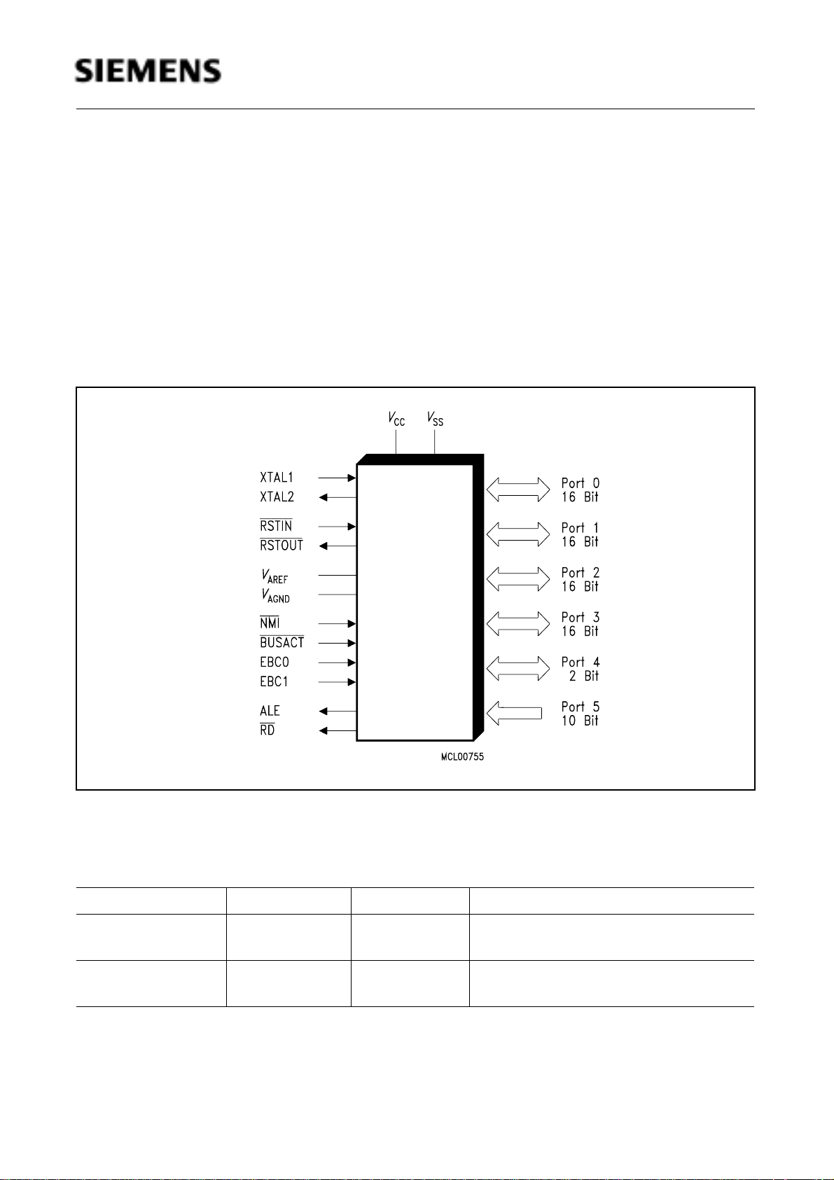
Figure 1
Logic Symbol
Ordering Information
Type Ordering Code Package Function
SAB 88C166-5M Q67120-C850 P-MQFP-100 16-bit microcontroller, 0 ˚C to + 70 ˚C,
1 KByte RAM, 32 KByte Flash EPROM
SAB 88C166W-5M Q67120-C934 P-MQFP-100 16-bit microcontroller, 0 ˚C to + 70 ˚C,
1 KByte RAM, 32 KByte Flash EPROM
Semiconductor Group 2
Page 4
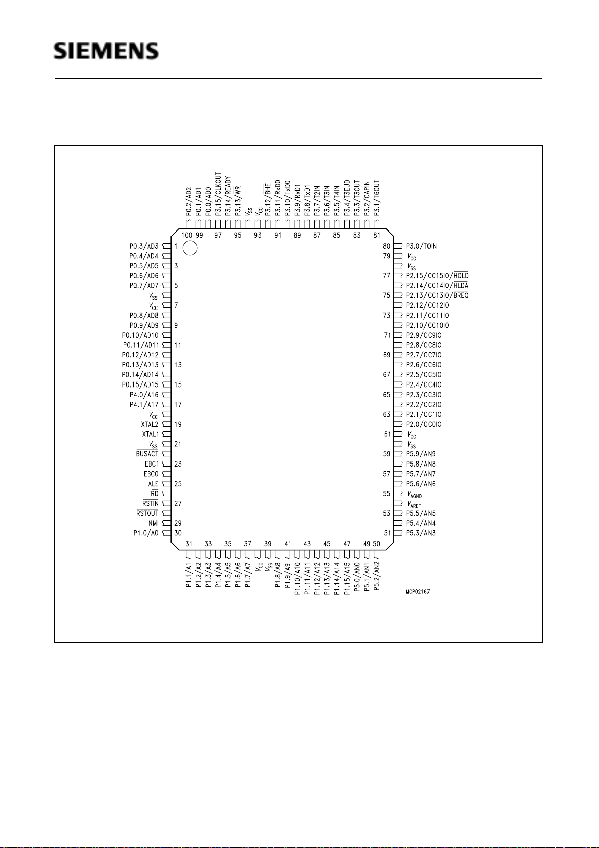
Pin Configuration Rectangular P-MQFP-100 (top view)
SAB 88C166(W)
Figure 2
SAB 88C166(W)
VPP /
Semiconductor Group 3
Page 5

Pin Definitions and Functions
SAB 88C166(W)
Symbol Pin
Number
P4.0 –
16 - 17
P4.1
16
17
XTAL1
XTAL2
BUSACT
EBC1,
EBC0
V
PP
RSTIN
RSTOUT
20
19
22
,
23
24
23
27 I Reset Input with Schmitt-Trigger characteristics. A low level at
28 O Internal Reset Indication Output. This pin is set to a low level
Input (I)
Output (O)
I/O
O
O
I
O
I
I
I
Function
Port 4 is a 2-bit bidirectional I/O port. It is bit-wise
programmable for input or output via direction bits. For a pin
configured as input, the output driver is put into highimpedance state.
In case of an external bus configuration, Port 4 can be used to
output the segment address lines:
P4.0 A16 Least Significant Segment Addr. Line
P4.1 A17 Most Significant Segment Addr. Line
XTAL1: Input to the oscillator amplifier and input to the
internal clock generator
XTAL2: Output of the oscillator amplifier circuit.
To clock the device from an external source, drive XTAL1,
while leaving XTAL2 unconnected. Minimum and maximum
high/low and rise/fall times specified in the AC Characteristics
must be observed.
External Bus Configuration selection inputs. These pins are
sampled during reset and select either the single chip mode
or one of the four external bus configurations:
BUSACT
EBC1 EBC0 Mode/Bus Configuration
0 0 0 8-bit demultiplexed bus
0 0 1 8-bit multiplexed bus
0 1 0 16-bit muliplexed bus
0 1 1 16-bit demultiplexed bus
1 0 0 Single chip mode
1 0 1 Reserved.
1 1 0 Reserved.
1 1 1 Reserved.
After reset pin EBC1 accepts the programming voltage for the
Flash EPROM as an “alternate function”:
Flash EPROM Programming Voltage V
= 12 V.
PP
this pin for a specified duration while the oscillator is running
resets the SAB 88C166(W). An internal pullup resistor permits
power-on reset using only a capacitor connected to V
SS
.
when the part is executing either a hardware-, a software- or a
watchdog timer reset. RSTOUT remains low until the EINIT
(end of initialization) instruction is executed.
Semiconductor Group 4
Page 6
Pin Definitions and Functions (cont’d)
SAB 88C166(W)
Symbol Pin
Number
NMI 29 I Non-Maskable Interrupt Input. A high to low transition at this
ALE 25 O Address Latch Enable Output. Can be used for latching the
RD
P1.0 –
P1.15
26 O External Memory Read Strobe. RD is activated for every
30 - 37
40 - 47
Input (I)
Output (O)
I/O Port 1 is a 16-bit bidirectional I/O port. It is bit-wise
Function
pin causes the CPU to vector to the NMI trap routine. When
the PWRDN (power down) instruction is executed, the NMI
pin must be low in order to force the SAB 88C166(W) to go
into power down mode. If NMI is high, when PWRDN is
executed, the part will continue to run in normal mode.
If not used, pull NMI high externally.
address into external memory or an address latch in the
multiplexed bus modes.
external instruction or data read access.
programmable for input or output via direction bits. For a pin
configured as input, the output driver is put into highimpedance state. Port 1 is used as the 16-bit address bus (A)
in demultiplexed bus modes and also after switching from a
demultiplexed bus mode to a multiplexed bus mode..
P5.0 –
P5.9
P2.0 –
P2.15
48 – 53
56 – 59II
62 – 77
62
...
75
76
77
I/O
I/O
I/O
O
I/O
O
I/O
I
Port 5 is a 10-bit input-only port with Schmitt-Trigger
characteristics. The pins of Port 5 also serve as the (up to 10)
analog input channels for the A/D converter, where P5.x
equals ANx (Analog input channel x).
Port 2 is a 16-bit bidirectional I/O port. It is bit-wise
programmable for input or output via direction bits. For a pin
configured as input, the output driver is put into highimpedance state.
The following Port 2 pins also serve for alternate functions:
P2.0 CC0IO CAPCOM: CC0 Cap.-In/Comp.Out
... ... ...
P2.13 CC13IO CAPCOM: CC13 Cap.-In/Comp.Out,
BREQ
P2.14 CC14IO CAPCOM: CC14 Cap.-In/Comp.Out,
HLDA External Bus Hold Acknowl. Output
P2.15 CC15IO CAPCOM: CC15 Cap.-In/Comp.Out,
HOLD External Bus Hold Request Input
External Bus Request Output
Semiconductor Group 5
Page 7
Pin Definitions and Functions (cont’d)
SAB 88C166(W)
Symbol Pin
Number
P3.0 –
P3.15
80 – 92,
95 – 97
80
81
82
83
84
85
86
87
88
89
90
91
92
95
96
97
Input (I)
Output (O)
I/O
I/O
I
O
I
O
I
I
I
I
O
I/O
O
I/O
O
O
I
O
Function
Port 3 is a 16-bit bidirectional I/O port. It is bit-wise
programmable for input or output via direction bits. For a pin
configured as input, the output driver is put into highimpedance state.
The following Port 3 pins also serve for alternate functions:
P3.0 T0IN CAPCOM Timer T0 Count Input
P3.1 T6OUT GPT2 Timer T6 Toggle Latch Output
P3.2 CAPIN GPT2 Register CAPREL Capture Input
P3.3 T3OUT GPT1 Timer T3 Toggle Latch Output
P3.4 T3EUD GPT1 Timer T3 Ext.Up/Down Ctrl.Input
P3.5 T4IN GPT1 Timer T4 Input for
Count/Gate/Reload/Capture
P3.6 T3IN GPT1 Timer T3 Count/Gate Input
P3.7 T2IN GPT1 Timer T2 Input for
Count/Gate/Reload/Capture
P3.8 TxD1 ASC1 Clock/Data Output (Asyn./Syn.)
P3.9 RxD1 ASC1 Data Input (Asyn.) or I/O (Syn.)
P3.10 T×D0 ASC0 Clock/Data Output (Asyn./Syn.)
P3.11 R×D0 ASC0 Data Input (Asyn.) or I/O (Syn.)
P3.12 BHE
Ext. Memory High Byte Enable Signal,
P3.13 WR External Memory Write Strobe
P3.14 READY Ready Signal Input
P3.15 CLKOUT System Clock Output (=CPU Clock)
P0.0 –
P0.15
V
AREF
V
AGND
98 – 5
8 – 15
I/O Port 0 is a 16-bit bidirectional IO port. It is bit-wise
programmable for input or output via direction bits. For a pin
configured as input, the output driver is put into highimpedance state.
In case of an external bus configuration, Port 0 serves as the
address (A) and address/data (AD) bus in multiplexed bus
modes and as the data (D) bus in demultiplexed bus modes.
Demultiplexed bus modes:
Data Path Width: 8-bit 16-bit
P0.0 – P0.7: D0 – D7 D0 - D7
P0.8 – P0.15: output! D8 - D15
Multiplexed bus modes:
Data Path Width: 8-bit 16-bit
P0.0 – P0.7: AD0 – AD7 AD0 - AD7
P0.8 – P0.15: A8 - A15 AD8 - AD15
54 - Reference voltage for the A/D converter.
55 - Reference ground for the A/D converter.
Semiconductor Group 6
Page 8

Pin Definitions and Functions (cont’d)
SAB 88C166(W)
Symbol Pin
Number
V
CC
7, 18,
38, 61,
79, 93
V
SS
6, 21,
39, 60,
78, 94
Input (I)
Function
Output (O)
- Digital Supply Voltage:
+ 5 V during normal operation and idle mode.
≥ 2.5 V during power down mode
- Digital Ground.
Functional Description
This document only describes specific properties of the SAB 88C166(W), e.g. Flash memory
functionality or specific DC and AC Characteristics, while for all other descriptions common for the
SAB 88C166(W) and the SAB 80C166(W)/83C166(W), e.g. functional description, it refers to the
respective Data Sheet for the Non-Flash device.
A detailled description of the SAB 88C166(W)’s instruction set can be found in the “C16x Family
Instruction Set Manual”.
Semiconductor Group 7
Page 9

SAB 88C166(W)
Memory Organization
The memory space of the SAB 88C166(W) is configured in a Von Neumann architecture which
means that code memory, data memory, registers and I/O ports are organized within the same
linear address space which includes 256 KBytes. Address space expansion to 16 MBytes is
provided for future versions. The entire memory space can be accessed bytewise or wordwise.
Particular portions of the on-chip memory have additionally been made directly bit addressable.
1 KByte of on-chip RAM is provided as a storage for user defined variables, for the system stack,
general purpose register banks and even for code. A register bank can consist of up to 16 wordwide
(R0 to R15) and/or bytewide (RL0, RH0, …, RL7, RH7) so-called General Purpose Registers
(GPRs).
512 bytes of the address space are reserved for the Special Function Register area. SFRs are
wordwide registers which are used for controlling and monitoring functions of the different on-chip
units. 98 SFRs are currently implemented. Unused SFR addresses are reserved for future
members of the SAB 80C166 family.
In order to meet the needs of designs where more memory is required than is provided on chip, up
to 256 KBytes of external RAM and/or ROM can be connected to the microcontroller.
Flash Memory Overview
The SAB 88C166(W) provides 32 KBytes of electrically erasable and reprogrammable non-volatile
Flash EPROM on-chip for code or constant data, which can be mapped to either segment 0
(0’0000H to 0’7FFFH) or segment 1 (1’0000H to 1’7FFFH) during the initialization phase.
A separate Flash Control Register (FCR) has been implemented to control Flash operations like
programming or erasure. For programming or erasing an external 12 V programming voltage must
be applied to the VPP/EBC1 pin.
The Flash memory is organized in 8 K x 32 bits, which allows even double-word instructions to be
fetched in just one machine cycle. The entire Flash memory is divided into four blocks with different
sizes (12/12/6/2 KByte). This allows to erase each block separately, when only parts of the Flash
memory need to be reprogrammed. Word or double word programming typically takes 100 µs, block
erasing typically takes 1 s (@ 20 MHz CPU clock). The Flash memory features a typical endurance
of 100 erasing/programming cycles. Erased Flash memory cells contain all ‘1’s, as known from
standard EPROMs.
The Flash memory can be programmed both in an appropriate programming board and in the target
system, which provides a lot of flexibility. The SAB 88C166(W)’s on-chip bootstrap loader may be
used to load and start the programming code.
To save the customer’s know-how, a Flash memory protection option is provided in the SAB
88C166(W). If this was activated once, Flash memory contents cannot be read from any location
outside the Flash memory itself.
Semiconductor Group 8
Page 10
SAB 88C166(W)
3’FFFF
3’0000
2’0000
1’0000
0’0000
H
3
H
Bank 3
Bank 2
2
Bank 1
H
1
H
Bank 0
0
H
Memory Segments Flash Banks
x’7800
x’6000
x’3000
x’0000
H
H
H
H
Figure 3
Flash Memory Overview
The Flash Control Register (FCR)
In standard operation mode the Flash memory can be accessed like the normal maskprogrammable on-chip ROM of the SAB 83C166. So all appropriate direct and indirect addressing
modes can be used for reading the Flash memory.
All programming or erase operations of the Flash memory are controlled via the 16-bit Flash control
register FCR. To prevent unintentional writing to the Flash memory the FCR is locked and inactive
during standard operation mode. Before a valid access to the FCR is enabled, the Flash memory
writing mode must be entered. This is done via a special key code instruction sequence.
Semiconductor Group 9
Page 11

SAB 88C166(W)
FCR (FFA0H / D0H) SFR Reset Value: 00X0
5 4 3 2 1 011 10 9 8 7 615 14 13 12
FWM
SET
rw
rw-rw-rw-rw-rw
- FWE
BE
WDW
W
CKCTL
VPP
REVFCVPP
FBUSY
RPROT
FEE
rw
*)
H
rwrw rrw rw r/wrw
Bit Function
FWE Flash Write Enable Bit (see description below)
0 : Flash write operations (program / erase) disabled
1 : Flash write operations (program / erase) enabled
FEE Flash Erase Enable Bit (Significant only, when FWE = ’1’, see description below)
0 : Flash programming mode selected
1 : Flash erase mode selected
FBUSY
Flash Busy Bit (On read accesses)
0 : No Flash write operation in progress
1 : Flash write operation in progress
RPROT
Flash Read Protection Activation Bit (On write accesses)
0 : Deactivates Flash read protection
1 : Activates Flash read protection, if this is enabled
FCVPP Flash Control V
PP
Bit
0 : No VPP failure occurred during a Flash write operation
1 : VPP failure occurred during a Flash write operation
VPPREV Flash V
0 : No valid VPP applied to pin V
Revelation Bit
PP
PP
1 : VPP applied to pin VPP is valid
CKCTL Internal Flash Timer Clock Control
Determines the width of an internal Flash write or erase pulse
WDWW Word / Double Word Writing Bit (significant only in programming mode)
0 : 16-bit programming operation
1 : 32-bit programming operation
BE Bank Erase Select (significant only in erasing mode)
Selects the Flash Bank to be erased
FWMSET Flash Writing Mode Set Bit (see description below)
0 : Exit Flash writing mode, return to standard mode
1 : Stay in Flash writing mode
*)
The reset value of bit VPPREV depends on the voltage on pin VPP.
Note: The FCR is no real register but is rather virtually mapped into the active address space of the
Flash memory while the Flash writing mode is active. In writing mode all direct (mem)
accesses refer to the FCR, while all indirect ([Rwn]) accesses refer to the Flash memory
array itself.
Semiconductor Group 10
Page 12

SAB 88C166(W)
The selection of Flash Operation and Read Mode is done via the three bits FWE, FEE and
FWMSET. The table below shows the combinations for these bits to select a specific function:
FWMSET FEE FWE Flash Operation Mode Flash Read Mode
1 1 1 Erasing mode Erase-Verify-Read via [Rn]
1 0 1 Programming mode Program-Verify-Read via [Rn]
1 X 0 Non-Verify mode Normal Read via [Rn]
0 X X Standard mode Normal Read via [Rn] or mem
FWE enables/disables write operations, FEE selects erasing or programming, FWMSET controls
the writing mode. Bits FWE and FEE select an operation, but do not execute it directly.
Note: Watch the FWMSET bit, when writing to register FCR (word access only), in order not to exit
Flash writing mode unintentionally by clearing bit FWMSET.
FBUSY: This read-only flag is set to ‘1’ while a Flash programming or erasing operation is in
progress. FBUSY is set via hardware, when the respective command is issued.
RPROT: This write-only Flash Read Protection bit determines whether Flash protection is active
or inactive. RPROT is the only FCR bit which can be modified even in the Flash standard mode but
only by an instruction executed from the on-chip Flash memory itself. Per reset, RPROT is set to ‘1’.
Note: RPROT is only significant, if the general Flash memory protection is enabled.
V
FCVPP and VPPREV: These read-only bits allow to monitor the
Revelation bit VPPREV reflects the state of the
‘0’ indicates that
V
is below the threshold value necessary for reliable programming or erasure,
PP
otherwise VPPREV = ‘1’). The Flash Control
V
voltage in the Flash writing mode (VPPREV =
PP
V
bit FCVPP indicates, if
PP
voltage. The Flash Vpp
PP
V
fell below the valid
PP
threshold value during a Flash programming or erase operation (FCVPP = ‘1’). FCVPP = ‘0’ after
such an operation indicates that no critical discontinuity on
V
has occurred.
PP
CKCTL: This Flash Timer Clock Control bitfield controls the width of the programming or erase
pulses (TPRG) applied to Flash memory cells during the corresponding operation. The width of a
single programming or erase pulse and the cumulated programming or erase time must not exceed
certain values to avoid putting the Flash memory under critical stress (see table below).
Time Specification Limit Value
Maximum Programming Pulse Width
Maximum Cumulated Programming Time
Maximum Erase Pulse Width
Maximum Cumulated Erase Time
128 µs
2.5 ms
10 ms
30 s
Semiconductor Group 11
Page 13
SAB 88C166(W)
In order not to exceed the limit values listed above, a specific CKCTL setting requires a minimum
CPU clock frequency, as listed below.
Setting of
CKCTL
0 0 2
0 1 2
1 0 2
1 1 2
Length of
TPRG
7
* 1/f
CPU
11
* 1/f
CPU
15
* 1/f
CPU
18
* 1/f
CPU
TPRG
@ f
CPU
= 20 MHz
f
CPUmin
for programming
f
CPUmin
for erasing
6.4 µs 1 MHz ---
102.4 µs 16 MHz 1 MHz
1.64 ms --- 3.28 MHz
13.11 ms --- 13.11 MHz
The maximum number of allowed programming or erase attempts depends on the CPU clock
frequency and on the CKCTL setting chosen in turn. This number results from the actual pulse width
compared to the maximum pulse width (see above tables).
The table below lists some sample frequencies, the respective recommended CKCTL setting and
the resulting maximum number of program / erase pulses:
f
CPU
CKCTL TPROG N
Programming Erasing
PROGmax
CKCTL TPROG N
ERASEmax
1 MHz 0 0 128 µs 19 0 1 2.05 ms 14648
10 MHz 0 0 12.8 µs 195 1 0 3.28 ms 9155
16 MHz 0 0 8 µs 312 1 0 2.05 ms 14648
20 MHz 0 0 6.4 µs 390 1 0 1.64 ms 18310
BE: The Flash Bank Erasing bit field determines the Flash memory bank to be erased (see table
below). The physical addresses of the selected bank depend on the Flash memory mapping
chosen.
BE setting Bank Addresses Selected for Erasure (x = 0 or 1)
0 0
0 1
1 0
1 1
0
1
2
3
x’0000
to x’2FFF
H
x’3000H to x’5FFF
x’6000H to x’77FF
x’7800H to x’7FFF
H
H
H
H
Semiconductor Group 12
Page 14
SAB 88C166(W)
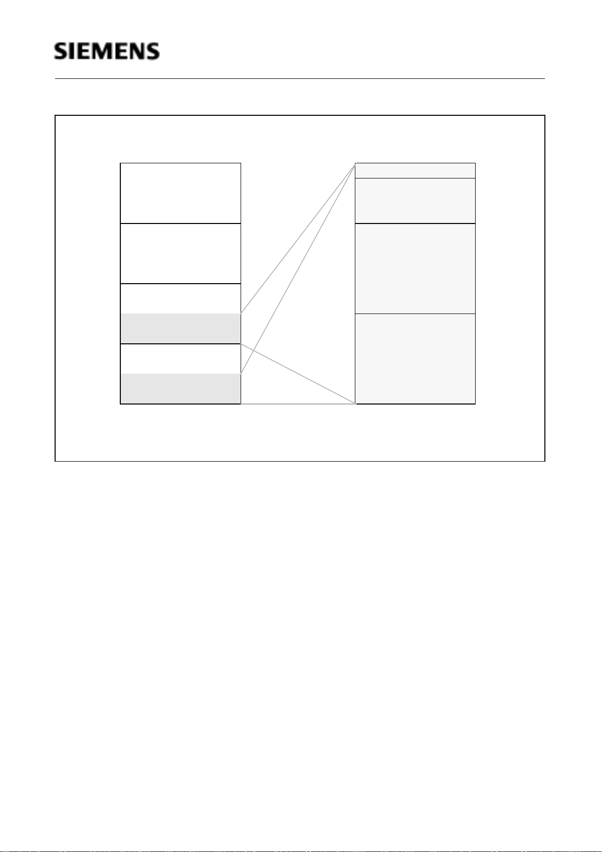
Operation Modes of the Flash Memory
There are two basic operation modes for Flash accesses: The standard and the writing mode. Submodes of the writing mode are the programming, the erase and the non-verify mode.
Figure 4
Flash Operating Mode Transitions
In Standard Mode the Flash memory can be accessed from any memory location (external
memory, on-chip RAM or Flash memory) for instruction fetches and data operand reads. Data
operand reads may use both direct 16-bit (mnemonic: mem) and indirect (mnemonic: [Rw])
addressing modes. Standard mode does not allow accesses to the FCR or Flash write operations.
Note: When Flash protection is active, data operands can be accessed only by instructions that are
executed out of the internal Flash memory.
The Flash Writing Modes must be entered for programming or erasing the Flash memory. The
SAB 88C166 enters these modes by a specific key code sequence, called UNLOCK sequence.
In writing mode the used addressing mode decides whether the FCR or a Flash memory location is
accessed. The FCR can be accessed with any direct access to an even address in the active
address space of the Flash memory. Only word operand instructions are allowed for FCR accesses.
Accesses to Flash memory locations must use indirect addressing to even addresses.
direct 16-bit addressing mode: mem --> Access to FCR
indirect addressing mode: [Rw
] --> Access to Flash location
n
Semiconductor Group 13
Page 15

SAB 88C166(W)
After entering writing mode the first erase or programming operation must not be started for at least
10 µs. This absolute (!) delay time is required to set up the internal high voltage. In general, Flash
write operations need a 12 V external
It is not possible to erase or to program the Flash memory via code executed from the Flash memory
itself. The respective code must reside within the on-chip RAM or within external memory.
When programming or erasing ‘on-line’ in the target system, some considerations have to be taken:
While these operations are in progress, the Flash memory cannot be accessed as usual. Therefore
care must be taken that no branch is taken into the Flash memory and that no data reads are
attempted from the Flash memory during programming or erasure. If the Flash memory is mapped
to segment 0, it must especially be ensured that no interrupt or hardware trap can occur, because
this would implicitly mean such a ‘forbidden’ branch to the Flash memory in this case.
The UNLOCK sequence is a specific key code sequence, which is required to enable the writing
modes of the SAB 88C166(W). The UNLOCK sequence must use identical values (see example
below) and must not be interrupted:
V
voltage to be applied to the
PP
V
PP
/EBC1 pin.
MOV FCR, Rw
MOV [Rw
], Rw
n
n
n
; Dummy write to the FCR
; Both operands use the same GPR
CALL cc_UC, WAIT_10 ; Delay for 10 µs (may be realized also by
; instructions other than a delay loop
where Rw
can be any word GPR (R0…R15). [Rwn] and FCR must point to even addresses within
n
the active address space of the Flash memory.
Note: Data paging and Flash segment mapping, if active, must be considered in this context.
In Flash Erase Mode (FEE=’1’, FWE=’1’) the SAB 88C166(W) is prepared to erase the bank
selected by the Bank Erase (BE) bit field in the FCR. The width of the erase pulses generated
internally is defined by the Internal Flash Timer Clock Control (CKCTL) bit field of the FCR. The
maximum number of erase pulses (EN
in the Flash erase algorithm. The chosen values for CKCTL and EN
) applied to the Flash memory is determined by software
max
must guarantee a maximum
max
cumulated erase time of 30 s per bank and a maximum erase pulse width of 20 ms.
The Flash bank erase operation will not start before the erase command is given. This provides
additional security for the erase operation. The erase command can be any write operation to a
Flash location, where the data and the even address written to must be identical:
MOV [Rwn], Rw
n
; Both operands use the same GPR
Upon the execution of this instruction, the Flash Busy (FBUSY) flag is automatically set to ‘1’
indicating the start of the operation. End of erasure can be detected by polling the FBUSY flag.
V
PP
must stay within the valid margins during the entire erase process.
At the end of erasure the Erase-Verify-Mode (EVM) is entered automatically. This mode allows to
check the effect of the erase operation (see description below).
Note: Before the erase algorithm can be properly executed, the respective bank of the Flash
memory must be programmed to all zeros (‘0000H’).
Semiconductor Group 14
Page 16

SAB 88C166(W)
In Flash Programming Mode (FEE=’0’, FWE=’1’) the SAB 88C166(W) is prepared to program
Flash locations in the way specified by the Word or Double Word Write (WDWW) bit in the FCR. The
width of the programming pulses generated internally is defined by the Internal Flash Timer Clock
Control (CKCTL) bit field of the FCR. The maximum number of programming pulses (PN
applied to the Flash memory is determined by software in the Flash programming algorithm. The
chosen values for CKCTL and PN
must guarantee a maximum cumulated programming time of
max
2.5 ms per cell and a maximum programming pulse width of 200 µs.
If 16-bit programming was selected, the operation will start automatically when an instruction is
executed, where the first operand specifies the address and the second operand the value to be
programmed:
max
)
MOV [Rwn], Rw
m
; Program one word
If 32-bit programming was selected, the operation will start automatically when the second of two
subsequent instructions is executed, which define the doubleword to be programmed. Note that the
destination pointers of both instructions refer to the same even double word address. The two
instructions must be executed without any interruption.
MOV [Rw
MOV [Rw
], Rw
n
], Rw
n
x
y
; Prepare programming of first word
; Start programming of both words
Upon the execution of the second instruction (the one and only in 16-bit programming mode), the
Flash Busy (FBUSY) bit is automatically set to ‘1’. End of programming can be detected by polling
the FBUSY bit.
V
must stay within the valid margins during the entire programming process.
PP
At the end of programming the Program-Verify-Mode (PVM) is entered automatically. This mode
allows to check the effect of the erase operation (see description below).
The Flash Verify-Modes Erase-Verify-Mode (EVM) and Program-Verify-Mode (PVM) allow to
verify the effect of an erase or programming operation. In these modes an internally generated
margin voltage is applied to a Flash cell, which makes reading more critical than for standard read
accesses. This ensures safe standard accesses after correct verification.
To get the contents of a Flash word in this mode, it has to be read in a particular way:
MOV Rw
, [Rwn] ; First (invalid) read of dedicated cell
m
… ; 4 µs delay to stabilize internal margin voltage
MOV Rw
, [Rwn] ; Second (valid) read of dedicated cell
m
Such a Flash verify read operation is different from the reading in the standard or in the non-verify
mode. Correct verify reading needs a read operation performed twice on the same cell with an
absolute time delay of 4 µs which is needed to stabilize the internal margin voltage applied to the
cell. To verify that a Flash cell was erased or programmed properly, the value of the second verify
read operation has to be compared against FFFFH or the target value, respectively. Clearing bit
FWE to ‘0’ exits the Flash programming mode and returns to the Flash non-verify mode.
In Flash non-verify mode all Flash locations can be read as usual (via indirect addressing modes),
which is not possible in Flash programming or Flash erase mode (see EVM and PVM).
Semiconductor Group 15
Page 17

SAB 88C166(W)
Flash Protection
If active, Flash protection prevents data operand accesses and program branches into the on-chip
Flash area from any location outside the Flash memory itself. Data operand accesses and branches
to Flash locations are exclusively allowed for instructions executed from the Flash memory itself.
Erasing and programming of the Flash memory is not possible while Flash protection is active.
Note: A program running within the Flash memory may of course access any location outside the
Flash memory and even branch to a location outside.
However, there is no way back, if Flash protection is active.
Flash protection is controlled by two different bits:
• The user-accessible write-only Protection Activation bit (RPROT) in register FCR and
• The one-time-programmable Protection Enable bit (UPROG).
Bit UPROG is a ‘hidden’ one-time-programmable bit only accessible in a special mode, which can
be entered eg. via a Flash EPROM programming board. Once programmed to ‘1’, this bit is
unerasable, ie. it is not affected by the Flash Erase mechanism.
To activate Flash Protection bit UPROG must have been programmed to ‘1’, and bit RPROT in
register FCR must be set to ‘1’. Both bits must be ‘1’ to activate Flash protection.
To deactivate Flash Protection bit RPROT in register FCR must be cleared to ‘0’. If any of the two
bits (UPROG or RPROT) is ‘0’, Flash protection is deactivated.
Generally Flash protection will remain active all the time. If it has to be deactivated intermittently, eg.
to call an external routine or to reprogram the Flash memory, bit RPROT must be cleared to ‘0’.
To access bit RPROT in register FCR, an instruction with a ‘mem, reg’ addressing mode must be
used, where the first operand has to represent the FCR address (any even address within the active
address space of the Flash memory) and the second operand must refer to a value which sets the
RPROT bit to ‘0’, eg.:
MOV FCR, ZEROS ; Deactivate Flash Protection
RPROT is the only bit in the FCR which can be accessed in Flash standard mode without having to
enter the Flash writing mode. Other bits in the FCR are not affected by such a write operation.
However, this access requires an instruction executed out of the internal Flash memory itself.
After reset bit RPROT is set to ’1’. For devices with protection disabled (UPROG=’0’) this has no
effect. For devices with protection enabled this ensures that program execution starts with Flash
protection active from the beginning.
Note: In order to maintain uninterrupted Flash protection, be sure not to clear bit RPROT
unintentionally by FCR write operations. Otherwise the Flash protection is deactivated.
Semiconductor Group 16
Page 18
SAB 88C166(W)
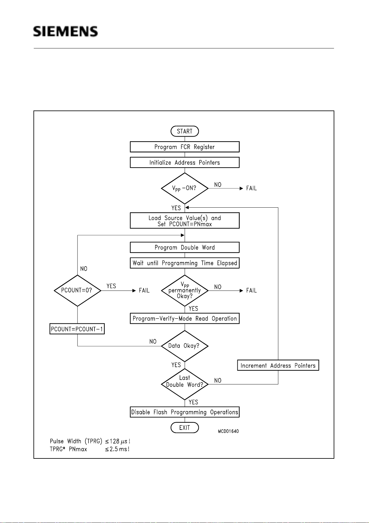
Flash Programming Algorithm
The figure below shows the recommended Flash programming algorithm. The following example
describes this algorithm in detail.
Figure 5
Flash Programming Algorithm
Semiconductor Group 17
Page 19

SAB 88C166(W)
Flash Programming Example
This example describes the Flash programming algorithm. A source block of code and/or data
within the first 32 Kbytes of segment 0 is copied (programmed) to a target block within the Flash
memory, which is mapped to segment 1 in this case. The start and the end address of the source
block to be copied are specified by the parameters SRC_START or SRC_END respectively. The
target Flash memory block begins at location FLASH_START. This example uses 32-bit Flash
programming.
Figure 6
Memory Allocation for Flash Programming Example
Note: This example represents one possibility how to program the Flash memory. Other solutions
may differ in the way they provide the source data (eg. without external memory), but use the
same Flash programming algorithm.
The FCR has been defined with an EQU assembler directive. Accesses to bits of the FCR are made
via an auxiliary GPR, as the FCR itself is not bit-addressable.
The shown example uses the following assumptions:
● Pin
● The SAB 88C166(W) runs at 20 MHz CPU clock (absolute time delays refer to it).
● The Flash memory is mapped to segment 1. All DPPs are set correctly.
V
/EBC1 receives a proper
PP
V
supply voltage.
PP
Semiconductor Group 18
Page 20

SAB 88C166(W)
● Enter writing mode via unlock sequence (prerequisite for any programming or erase
operation).
MOV FCR, Rw
MOV [Rw
], Rw
n
n
n
; Dummy write to the FCR
; Both operands use the same GPR
CALL cc_UC, WAIT_10 ; Delay for 10 µs
● Program the FCR register with a value that selects the desired operating mode. Note that this
does not yet start the programming operation itself.
MOV R15, #1000 0000 1010 0001B
; #xxxx xxxx xxxx xxx1: FWE=’1’: Enable Flash write operations
; #xxxx xxxx xxxx xx0x: FEE=’0’: Select programming mode
; #xxxx xxxx x01x xxxx: CKCTL=’01’: 100 µs programming pulse (fCPU = 20 MHz)
; #xxxx xxxx 1xxx xxxx: WDWW=’1’: Select 32-bit programming mode
; #1xxx xxxx xxxx xxxx: FWMSET=’1’: Stay in writing mode
MOV DPP1:pof FCR, R15 ; Write Value to the FCR using 16-bit access
● Initialize pointers and counter for the first transfer of the programming algorithm.
The source data block is accessed via the pointer SRC_PTR, initialized with SRC_START. All
read operations via SRC_PTR use DPP2, which selects data page 1 in this example.
The Flash memory must be accessed indirectly and uses the pointer FLASH_PTR, initialized
with FLASH_START.
The counter DWCOUNT defines the number of doublewords to be programmed.
● Test for correct
V
margin at pin
PP
V
/EBC1 before a programming operation is started. If bit
PP
VPPREV reads ‘1’, the programming voltage is correct and the algorithm can be continued.
V
Otherwise, the programming routine could wait in Flash writing mode until
reaches its correct
PP
value and resume programming then, or it could exit writing mode.
MOV R15, DPP1:pof FCR ; Read FCR contents using 16-bit access
JB R15.4, Vpp_OK1 ; Test
V
via bit VPPREV (= FCR.4)
PP
… ; VPPREV=’0’: Exit programming procedure
Vpp_OK1: ; VPPREV=’1’: Test Okay! Continue
Semiconductor Group 19
Page 21

SAB 88C166(W)
● Load source values and initialize loop counter (PCOUNT) with the maximum number of
programming trials (PNmax) to be performed before exiting the routine with a failure. Each trial
means applying a pulse of 100 µs to the selected words in the Flash memory. According to the
maximum cumulated programming time of 2.5 ms allowed per cell, PNmax must be ‘25’ here.
The doubleword at memory location [SRC_PTR] is loaded into two auxiliary registers DATAWR1
and DATAWR2.
● Program one doubleword stored in the auxiliary data registers to the Flash memory location
[FLASH_PTR]. FLASH_PTR is not incremented here, since in 32-bit programming mode the
hardware automatically arranges the two data words correctly. The execution of the second write
instruction automatically starts the programming of the entire double word.
This instruction sequence must not be interrupted.
MOV [FLASH_PTR], DATAWR1 ; Write low word to Flash
MOV [FLASH_PTR], DATAWR2 ; Write high word to Flash, starts programming
● Wait until programming time elapsed (100 µs in this example), which depends on bit field
CKCTL in the FCR register and on the CPU clock frequency. End of programming is detected by
polling the FBUSY flag in the FCR register. The Flash memory switches to PVM mode
automatically.
WAIT_PROG: ; Polling Loop to check bit FBUSY
MOV R15, DPP1: pof FCR ; Read FCR contents using 16-bit access
JB R15.2, WAIT_PROG ; Loop while bit FBUSY (FCR.2) is ‘1’
… ; Continue in PVM mode, when FBUSY is ‘0’
● Verify
V
validity during programming to make sure
PP
V
did not exceed its valid margins
PP
during the programming operation. Otherwise programming may have not been performed
properly. The FCVPP flag is set to ‘1’ in case of this error condition. If FCVPP reads ‘1’, the
programming routine can abort, when
V
proves to be stable now.
PP
V
still fails, or repeat the programming operation, when
PP
Semiconductor Group 20
Page 22

SAB 88C166(W)
● Perform Program-Verify operation and compare with source data in order to check whether
a programming operation was performed correctly. PVM reading consists of two identical Flash
read instructions with 4 µs delay in between. This example uses CMP instructions to access the
Flash memory. In case of a mismatch the programming routine repeats the programming cycle
provided that the maximum number of attempts was not yet reached. PVM reading and data
comparison must be performed on both words of the double word to be tested.
CMP DATAWR1, [FLASH_PTR] ; 1st step of PVM read (low word)
CALL cc_UC, WAIT_4 ; Delay for 4 µs
CMP DATAWR1, [FLASH_PTR] ; 2nd step of PVM read (low word)
JMP cc_NZ, PROG_FAILED ; Reprogram on mismatch, if (PCOUNT) > 0
MOV R15, FLASH_PTR
ADD R15, #0002H ; Auxiliary pointer to upper word of doubleword
CMP DATAWR2, [R15] ; 1st step of PVM read (high word)
CALL cc_UC, WAIT_4 ; Delay for 4 µs
CMP DATAWR2, [R15] ; 2nd step of PVM read (high word)
JMP cc_NZ, PROG_FAILED ; Reprogram on mismatch, if (PCOUNT) > 0
. . . ; Programming was OK. Go on with next step.
● Check number of programming attempts to decide, if another programming attempt is
allowed. PCOUNT is decremented by ‘1’ upon each unsuccessful programming attempt. If it
expires, the failing Flash cells are classified as unprogrammable and should be left out. This
failure is very unlikely to occur. However, it should be checked for safe programming.
Note: This step is taken only in case of a program verify mismatch.
● Check for last doubleword and increment pointers to decide, if another programming cycle is
required. The auxiliary counter DWCOUNT is decremented by ‘1’ after each successful double
word programming. If it expires, the complete data block is programmed and the programming
routine is exited successfully. Otherwise source and target pointers (SRC_PTR and
FLASH_PTR) are incremented to the next doubleword to be programmed.
● Disable Flash programming operations and exit routine, when the Flash memory block was
programmed successfully or when a failure occurred. In either case bit FWE of the FCR is reset
to ‘0’ and the programming routine is exited. This means that the Flash non-verify mode is
entered again, where the FCR stays accessible but Flash memory locations can be read
normally again using indirect addressing. For returning to the Flash standard mode, bit FWMSET
of the FCR must be reset to ‘0’ by the calling routine. The programming routine may return an exit
code that indicates correct programming or identifies the type of error.
Semiconductor Group 21
Page 23

SAB 88C166(W)
Flash Erase Algorithm
The figure below shows the recommended Flash erase algorithm. The following example describes
this algorithm in detail.
Figure 7
Flash Erase Algorithm
Semiconductor Group 22
Page 24

SAB 88C166(W)
Flash Erase Example
This example describes the Flash erase algorithm. The four banks of the Flash memory can be
erased separately. The algorithm erases the Flash memory bank, which is selected by bitfield BE in
the FCR. Start address and size of the selected Flash bank have to be considered.
Note: Before a bank can be erased, all its contents must be programmed to ‘0000H’. This is
required by the physics of the Flash memory cells and is done with the Flash programming
algorithm already described.
Figure 8
Memory Banking for Flash Erasure
The FCR has been defined with an EQU assembler directive. Accesses to bits of the FCR are made
via an auxiliary GPR, as the FCR itself is not bit-addressable.
The shown example uses the following assumptions:
● Pin
● The SAB 88C166(W) runs at 20 MHz CPU clock (absolute time delays refer to it).
● The Flash memory is mapped to segment 1. All DPPs are set correctly.
V
/EBC1 receives a proper
PP
V
supply voltage.
PP
Semiconductor Group 23
Page 25

SAB 88C166(W)
● Enter writing mode via unlock sequence (prerequisite for any programming or erase
operation).
MOV FCR, Rw
MOV [Rw
], Rw
n
n
n
; Dummy write to the FCR
; Both operands use the same GPR
CALL cc_UC, WAIT_10 ; Delay for 10 µs
● Program the FCR register with a value that selects erase mode. Note that this does not yet start
the erase operation itself.
MOV R15, #1000 00XX 0110 0011B
; #xxxx xxxx xxxx xxx1: FWE=’1’: Enable Flash write operations
; #xxxx xxxx xxxx xx1x: FEE=’1’: Select erase mode
; #xxxx xxxx x11x xxxx: CKCTL=’11’: 10 ms erase pulse (fCPU = 20 MHz)
; #xxxx xxXX xxxx xxxx: BE=’xx’: Select the desired bank (3...0)
; #1xxx xxxx xxxx xxxx: FWMSET=’1’: Stay in writing mode
MOV DPP1:pof FCR, R15 ; Write Value to the FCR using 16-bit access
● Initialize target pointer with the start address of the selected Flash memory bank. The Flash
memory must be accessed indirectly and uses the pointer FLASH_PTR. This pointer will apply
to DPP0 or DPP1, which are expected to select data pages 4 or 5, respectively.
● Test for correct
V
margin at pin
PP
V
/EBC1 before an erase operation is started. If bit
PP
VPPREV reads ‘1’, the erase voltage is correct and the algorithm can be continued. Otherwise,
the erase routine could wait in Flash writing mode until
V
reaches its correct value and resume
PP
erasing then, or it could exit writing mode.
MOV R15, DPP1:pof FCR ; Read FCR contents using 16-bit access
JB R15.4, Vpp_OK2 ; Test
V
via bit VPPREV (= FCR.4)
PP
… ; VPPREV=’0’: Exit erase procedure
Vpp_OK2: ; VPPREV=’1’: Test Okay! Continue
● Initialize loop counter (PCOUNT) with the maximum number of erase trials (ENmax) to be
performed before exiting the routine with a failure. Each trial means applying a pulse of 10 ms to
the selected Flash memory bank. According to the maximum cumulated erase time of 30 s
allowed per cell, ENmax must be ‘3000’ here.
● Erase selected Flash memory bank by writing to a Flash memory location using the target
address as write data.
MOV [FLASH_PTR], FLASH_PTR ; Write address to Flash, starts erasing
● Wait until erase time elapsed, which depends on bit field CKCTL in the FCR register and on the
CPU clock frequency (10 ms in this example). End of erasing is detected by polling the FBUSY
flag in the FCR register. The Flash memory switches to EVM mode automatically.
Semiconductor Group 24
Page 26

SAB 88C166(W)
WAIT_ERASE: ; Polling Loop to check bit FBUSY
MOV R15, DPP1: pof FCR ; Read FCR contents using 16-bit access
JB R15.2, WAIT_ERASE ; Loop while bit FBUSY (FCR.2) is ‘1’
… ; Continue in EVM mode, when FBUSY is ‘0’
● Verify
V
validity during erasing to make sure
PP
V
did not exceed its valid margins during the
PP
erase operation. Otherwise erasing may have not been performed properly. The FCVPP flag is
set to ‘1’ in case of this error condition. If FCVPP reads ‘1’, the erase routine can abort, when
still fails, or repeat the erase operation, when
● Perform Erase-Verify operation and compare with ‘FFFF
V
proves to be stable now.
PP
’ in order to check whether an
H
V
PP
erase operation was performed correctly. EVM reading consists of two identical Flash read
instructions with 4 µs delay in between. This example uses CMP instructions to access the Flash
memory. In case of a mismatch the erase routine repeats the erase cycle provided that the
maximum number of attempts was not yet reached.
MOV R15, ONES ; Load auxiliary GPR with anticipated value
CMP R15, [FLASH_PTR] ; 1st step of EVM read
CALL cc_UC, WAIT_4 ; Delay for 4 µs
CMP R15, [FLASH_PTR] ; 2nd step of EVM read
JMP cc_NZ, ERASE_FAILED ; Re-erase on mismatch, if (PCOUNT) > 0
. . . ; Erasing was OK. Go on with next step.
● Check number of erase attempts to decide, if another erase attempt is allowed. PCOUNT is
decremented by ‘1’ upon each unsuccessful erase attempt. If it expires, the failing Flash memory
bank is classified as unerasable. This failure is very unlikely to occur. However, it should be
checked for safe erasing.
Note: This step is taken only in case of a erase verify mismatch.
● Check for last word and increment pointers to decide, if another cell must be verified. The
target pointer (FLASH_PTR) is incremented to the next word to be verified and checked against
the upper limit of the respective bank. If the target pointer exceeds the bank limit, the erase
routine is exited successfully.
● Disable erase operations and exit routine, when the Flash memory bank was erased
successfully or when a failure occurred. In either case bit FWE of the FCR is reset to ‘0’ and the
erase routine is exited. This means that the Flash non-verify mode is entered again, where the
FCR stays accessible but Flash memory locations can be read normally again using indirect
addressing. For returning to the Flash standard mode, bit FWMSET of the FCR must be reset to
‘0’ by the calling routine. The erase routine may return an exit code that indicates correct erasing
or identifies the type of error.
Semiconductor Group 25
Page 27

SAB 88C166(W)
Fundamentals of Flash Technology
The Flash memory included in the SAB 88C166(W) combines the EPROM programming
mechanism with electrical erasability (like an EEPROM) to create a highly reliable and cost effective
memory. A Flash memory cell consists of a single transistor with a floating gate for charge storage
like an EPROM, uses a thinner gate oxide, however.
The programming mechanism of a Flash cell is based on ‘hot’ electron injection which works as
follows: The high voltage between drain and source forces ‘hot’ electrons supplied from the source
to enter the channel. Attracted by the high voltage on the cell’s control gate there, free electrons are
trapped into the floating gate. The amount of negative charge on the floating gate is basically
determined by the length and the number of programming pulses applied to the cell. A special read
operation, Program-Verify, is provided for verifying that the charge put onto the floating gate
represents a proper ‘0’.
Figure 9
Flash Memory Cell Programming Mechanism
The cell erase mechanism is based on ‘Fowler-Nordheim’ tunnelling which works as follows:
A high voltage is applied to the cell’s source whilst the control gate grounded. The cell’s drain is
disconnected in this case. Attracted by the high voltage on the cell’s source, electrons migrate from
the floating gate to the source. The amount of negative charge removed from the floating gate is
basically determined by the length and the number of erasing pulse applied to the cell. A special
read operation, Erase-Verify, is provided for verifying that the charge remaining on the floating gate
represents a proper ‘1’.
Unlike a standard EEPROM, where individual bytes can be erased, the Flash memory of the SAB
88C166(W) is erased block-wise which means that the high voltage is applied to all cells belonging
to one block simultaneously.
One requirement for performing proper Flash programming and erase operations is to have all cells
of a block set to a minimum threshold level before the operation is started. A cell erasing faster than
others could have a threshold voltage too low or negative. In this case the corresponding transistor
could become conductive and affect other cells placed in the same column of the transistor array.
Thus, all cells of that column could erroneously be read as ‘1’ instead of ‘0’.
Semiconductor Group 26
Page 28

SAB 88C166(W)
To avoid this possible malfunction, the user must equalize the amount of charge on each cell by
programming all cells of one block to ‘0’ before performing a block erasure.
Figure 10
Flash Memory Cell Erase Mechanism
The introduced erase algorithm meets this requirement. In combination with the Flash technology
used, it provides a tight threshold voltage distribution, generating a sufficient margin even to cells
erasing faster than others.
Figure 11
Flash Erasure
Note that the following terminology is used in this document: Flash WRITING means changing the
state of the floating gate. Flash PROGRAMMING means loading electrons onto the floating gate.
Flash ERASING means removing electrons from the floating gate.
Semiconductor Group 27
Page 29

SAB 88C166(W)
Absolute Maximum Ratings
Ambient temperature under bias (TA):
SAB 88C166(W)-5M.......................................................................................................0 to + 70 ˚C
Storage temperature (TST) ....................................................................................... – 65 to + 125 ˚C
Voltage on VCC pins with respect to ground (VSS) ..................................................... – 0.5 to + 6.5 V
Voltage on any pin with respect to ground (VSS).................................................– 0.5 to VCC + 0.5 V
Input current on any pin during overload condition.................................................. – 10 to + 10 mA
Absolute sum of all input currents during overload condition ..............................................|100 mA|
Power dissipation........................................................................................................................ 1 W
Flash programming voltage (VPP)............................................................................ – 0.3 to + 13.5 V
Note: Stresses above those listed under “Absolute Maximum Ratings” may cause permanent
damage to the device. This is a stress rating only and functional operation of the device at
these or any other conditions above those indicated in the operational sections of this
specification is not implied. Exposure to absolute maximum rating conditions for extended
periods may affect device reliability. During overload conditions (VIN > VCC or VIN < VSS) the
voltage on pins with respect to ground (VSS) must not exceed the values defined by the
Absolute Maximum Ratings.
Parameter Interpretation
The parameters listed in the following partly represent the characteristics of the SAB 88C166(W)
and partly its demands on the system. To aid in interpreting the parameters right, when evaluating
them for a design, they are marked in column “Symbol”:
CC (Controller Characteristics):
The logic of the SAB 88C166(W) will provide signals with the respective timing characteristics.
SR (System Requirement):
The external system must provide signals with the respective timing characteristics to the SAB
88C166(W).
Semiconductor Group 28
Page 30

SAB 88C166(W)
DC Characteristics
V
= 5 V ± 10 %; VSS = 0 V; f
CC
T
= 0 to + 70 ˚C for SAB 88C166(W)-5M
A
Parameter Symbol Limit Values Unit Test Condition
= 20 MHz
CPU
min. max.
Input low voltage EBC1/V
PP
V
SR – 0.3 0.2 V
IL1
CC
V–
– 0.1
Input low voltage
(all except EBC1/V
PP
)
Input high voltage
(all except RSTIN
and XTAL1)
Input high voltage RSTIN
Input high voltage XTAL1
Output low voltage
(Port 0, Port 1, Port 4, ALE, RD
SR – 0.5 0.2 V
IL2
CC
– 0.1
V
SR 0.2 V
IH
CC
V
+ 0.5 V –
CC
+ 0.9
V
SR 0.6 V
IH1
V
SR 0.7 V
IH2
V
CC – 0.45 V IOL = 2.4 mA
OL
CC
CC
V
+ 0.5 V –
CC
V
+ 0.5 V –
CC
,
V–
V
WR, BHE, CLKOUT, RSTOUT)
Output low voltage
V
CC – 0.45 V I
OL1
= 1.6 mA
OL1
(all other outputs)
Output high voltage
(Port 0, Port 1, Port 4, ALE, RD
CC 0.9 V
OH
,
CC
2.4
–VI
= – 500 µA
OH
I
= – 2.4 mA
OH
V
WR, BHE, CLKOUT, RSTOUT)
Output high voltage
(all other outputs)
Input leakage current (Port 5)
1)
Input leakage current (all other) I
VPP leakage current EBC1/V
PP
RSTIN pullup resistor R
Read inactive current
Read active current
ALE inactive current
ALE active current
4)
4)
4)
4)
CC 0.9 V
OH1
CC
2.4
I
CC – ± 200 nA 0 V < VIN < V
OZ1
CC – ± 500 nA 0 V < VIN < V
OZ2
I
CC – ± 100 µA VPP ≤ V
PPS
CC 50 150 kΩ –
RST
2)
I
RH
I
RL
I
ALEL
I
ALEH
3)
– – 40 µA V
-500 – µA V
2)
– 150 µA V
3)
2100 – µA V
–V
V
I
= – 250 µA
OH
I
= – 1.6 mA
OH
OUT
OUT
OUT
OUT
= V
= V
= V
= V
CC
OHmin
OLmax
OLmax
OHmin
V
XTAL1 input current IILCC – ± 20 µA 0 V < VIN < V
Pin capacitance
(digital inputs/outputs)
Power supply current
Idle mode supply current I
5)
C
CC – 10 pF f = 1 MHz
IO
T
A
I
CC
ID
– 50 +
5 x f
– 30 +
1.5 x f
CPU
CPU
mA RSTIN = V
f
CPU
mA RSTIN = V
f
CPU
= 25 ˚C
IL2
in [MHz]
IH1
in [MHz]
CC
CC
CC
6)
6)
Semiconductor Group 29
Page 31

SAB 88C166(W)
Parameter Symbol Limit Values Unit Test Condition
min. max.
Power-down mode supply current I
V
read current I
PP
V
writing current I
PP
PD
PPR
PPW
–50µAV
= 5.5 V
CC
– 200 µA VPP > V
– 50 mA 1/TCL = 40 MHz
32-bit
programming
V
= 12 V
PP
V
during write/read V
PP
PP
Notes
1)
This specification does not apply to the analog input (Port 5.x) which is currently converted.
2)
The maximum current may be drawn while the respective signal line remains inactive.
3)
The minimum current must be drawn in order to drive the respective signal line active.
4)
This specification is only valid during Reset, or during Hold-mode.
5)
Not 100% tested, guaranteed by design characterization.
6)
The supply current is a function of the operating frequency. This dependency is illustrated in the figure below.
These parameters are tested at V
or VIH.
V
IL
7)
All inputs (including pins configured as inputs) at 0 V to 0.1 V or at VCC – 0.1 V to VCC, V
and 20 MHz CPU clock with all outputs disconnected and all inputs at
CCmax
(including pins configured as outputs) disconnected.
A voltage of V
≥ 2.5 V is sufficient to retain the content of the internal RAM during power down mode.
CC
11.4 12.6 V
= 0 V, all outputs
REF
7)
CC
Semiconductor Group 30
Page 32

150
100
I [mA]
SAB 88C166(W)
I
CCmax
50
10
5 10
15 20
Figure 12
Supply/Idle Current as a Function of Operating Frequency
I
IDmax
f
CPU
[MHz]
Semiconductor Group 31
Page 33

SAB 88C166(W)
A/D Converter Characteristics
V
= 5 V ± 10 %; VSS = 0 V
CC
T
= 0 to + 70 ˚C for SAB 88C166(W)-5M
A
4.0 V ≤ V
Parameter Symbol Limit Values Unit Test Condition
Analog input voltage range
Sample time tSCC – 2 t
Conversion time tCCC – 10 tCC +
Total unadjusted error TUECC – ± 2 LSB
Internal resistance of reference
voltage source
Internal resistance of analog
source
ADC input capacitance C
≤ VCC + 0.1 V; VSS – 0.1 V ≤ V
AREF
≤ VSS + 0.2 V
AGND
min. max.
V
SR V
AIN
R
CC – tCC / 250
AREF
AGND
V
AREF
SC
t
+ 4TCL
S
- 0.25
R
CC – tS / 500
ASRC
– 0.25
CC – 50 pF
AIN
V
kΩ
kΩ
1)
2) 4)
3) 4)
5)
t
in [ns]
CC
t
in [ns]
S
7)
6) 7)
2) 7)
Notes
1)
V
may exceed V
AIN
cases will be X000
2)
During the sample time the input capacitance CI can be charged/discharged by the external source. The
or V
AGND
or X3FFH, respectively.
H
up to the absolute maximum ratings. However, the conversion result in these
AREF
internal resistance of the analog source must allow the capacitors to reach their final voltage level within t
After the end of the sample time t
The value for the sample clock is t
3)
This parameter includes the sample time tS, the time for determining the digital result and the time to load the
, changes of the analog input voltage have no effect on the conversion result.
S
= TCL x 32.
SC
result register with the conversion result.
The value for the conversion clock is t
4)
This parameter depends on the ADC control logic. It is not a real maximum value, but rather a fixum.
5)
TUE is tested at V
AREF
= 5.0 V, V
= TCL x 32.
CC
= 0 V, VCC = 4.8 V. It is guaranteed by design characterization for all
AGND
other voltages within the defined voltage range.
6)
During the conversion the ADC’s capacitance must be repeatedly charged or discharged. The internal
resistance of the reference voltage source must allow the capacitors to reach their respective voltage level
within t
7)
Not 100% tested, guaranteed by design characterization.
. The maximum internal resistance results from the CPU clock period.
CC
.
S
Semiconductor Group 32
Page 34

SAB 88C166(W)
Testing Waveforms
AC inputs during testing are driven at 2.4 V for a logic ‘1’ and 0.4 V for a logic ‘0’.
Timing measurements are made at V
Figure 13
Input Output Waveforms
min for a logic ‘1’ and VIL max for a logic ‘0’.
IH
For timing purposes a port pin is no longer floating when a 100 mV change from load
voltage occurs, but begins to float when a 100 mV change from the loaded VOH/VOL level occurs
(IOH/IOL = 20 mA).
Figure 14
Float Waveforms
Memory Cycle Variables
The timing tables below use three variables which are derived from registers SYSCON and
BUSCON1 and represent the special characteristics of the programmed memory cycle. The
following table describes, how these variables are to be computed.
Description Symbol Values
ALE Extension
Memory Cycle Time Waitstates
Memory Tristate Time
t
A
t
C
t
F
TCL x <ALECTL>
2TCL x (15 – <MCTC>)
2TCL x (1 – <MTTC>)
Semiconductor Group 33
Page 35

SAB 88C166(W)
AC Characteristics
The specification of the timings depends on the CPU clock signal that is used in the respective
device. In this regard the specification for the SAB 88C166 and the SAB 88C166W are different.
While the SAB 88C166W directly uses the clock signal fed to XTAL1 and therefore has to take into
account the duty cycle variation of this signal, the SAB 88C166 derives its CPU clock from the
XTAL1 signal via a 2:1 prescaler and therefore is independant from these variations.
For these reasons the following pages provide the timing specifications for SAB 88C166 and for
SAB 88C166W separately (where applicable).
AC Characteristics
External Clock Drive XTAL1 for the SAB 88C166
V
= 5 V ± 10 %; VSS = 0 V
CC
T
= 0 to +70 ˚C for SAB 88C166-5M
A
Parameter Symbol Max. CPU Clock
= 20 MHz
Variable CPU Clock
1/2TCL = 1 to 20 MHz
Unit
min. max. min. max.
Oscillator period TCLSR 25 25 25 500 ns
t
High time
Low time
Rise time
Fall time
SR6–6–ns
1
t
SR6–6–ns
2
t
SR–5–5ns
3
t
SR–5–5ns
4
Figure 15
External Clock Drive XTAL1
Semiconductor Group 34
Page 36

AC Characteristics (cont’d)
External Clock Drive XTAL1 for the SAB 88C166W
V
= 5 V ± 10 %; VSS = 0 V
CC
T
= 0 to + 70 ˚C for SAB 88C166W-M
A
SAB 88C166(W)
Parameter Symbol CPU Clock = 16 MHz
Duty cycle 0.4 to 0.6
Variable CPU Clock
1/CLP = 1 to 20 MHz
Unit
min. max. min. max.
Oscillator period CLPSR 62.5 62.5 50 1000 ns
High time TCL
Low time TCL
Rise time
Fall time
SR 25 – 25 CLP-TCL
H
SR 25 – 25 CLP-TCL
L
t
SR – 10 – 10 ns
R
t
SR – 10 – 10 ns
F
L
H
ns
ns
Oscillator duty cycle DCSR 0.4 0.6 25 / CLP 1 – 25 / CLP
Clock cycle TCLSR 25 37.5 CLP x DC
min
CLP x DC
max
ns
Note: In order to run the SAB 88C166W at a CPU clock of 20 MHz the duty cycle of the oscillator
clock must be 0.5, ie. the relation between the oscillator high and low phases must be 1:1. So
the variation of the duty cycle of the oscillator clock limits the maximum operating speed of
the device.
The 16 MHz values in the tables are given as an example for a typical duty cycle variation of
the oscillator clock from 0.4 to 0.6.
Figure 16
External Clock Drive XTAL1
Semiconductor Group 35
Page 37

SAB 88C166(W)
AC Characteristics (cont’d)
Multiplexed Bus for the SAB 88C166
V
= 5 V ± 10 %; VSS = 0 V
CC
T
= 0 to + 70 ˚C for SAB 88C166-5M
A
C
(for Port 0, Port 1, Port 4, ALE, RD, WR, BHE, CLKOUT) = 100 pF
L
ALE cycle time = 6 TCL + 2tA + tC + tF (150 ns at 20-MHz CPU clock without waitstates)
Parameter Symbol Max. CPU Clock
= 20 MHz
min. max. min. max.
ALE high time t5CC 15 + t
t
t
t
CC
6
CC
7
CC
8
10 +
15 +
15 +
Address setup to ALE
Address hold after ALE
ALE falling edge to RD
,
A
t
A
t
A
t
A
– TCL – 10 + tA–ns
– TCL – 15 + tA–ns
– TCL – 10 + tA–ns
– TCL – 10 + tA–ns
WR (with RW-delay)
t
ALE falling edge to RD
,
CC
9
– 10 +
t
– – 10 + t
A
WR (no RW-delay)
t
Address float after RD
,
10
CC
–5–5ns
WR (with RW-delay)
t
Address float after RD
,
11
CC
– 30 – TCL + 5 ns
WR (no RW-delay)
, WR low time
RD
t
CC 40 + t
12
C
– 2TCL – 10
(with RW-delay)
WR low time
RD
t
CC 65 + t
13
C
– 3TCL – 10
(no RW-delay)
to valid data in
RD
t
SR – 30 + t
14
C
(with RW-delay)
to valid data in
RD
t
SR – 55 + t
15
C
(no RW-delay)
ALE low to valid data in
t
SR – 55
16
+ tA + t
t
Address to valid data in
SR – 75
17
+ 2tA + t
t
Data hold after RD
SR0–0–ns
18
rising edge
Variable CPU Clock
1/2TCL = 1 to 20 MHz
A
+ t
C
+ t
C
– 2TCL – 20
– 3TCL – 20
– 3TCL – 20
C
– 4TCL – 25
C
Unit
–ns
–ns
–ns
ns
+ t
C
ns
t
+
C
ns
+ tA + t
C
ns
+ 2tA + t
C
t
Data float after RD
Data valid to WR
Data hold after WR
SR – 35 + t
19
t
CC 35 + t
22
t
CC 35 + t
23
C
F
Semiconductor Group 36
F
– 2TCL – 15
– 2TCL – 15
+ t
C
– 2TCL – 15
+ t
F
ns
+ t
F
–ns
–ns
Page 38

SAB 88C166(W)
Parameter Symbol Max. CPU Clock
= 20 MHz
min. max. min. max.
ALE rising edge after RD,
t
CC 35 + t
25
F
– 2TCL – 15
WR
Address hold after RD
,
t
CC 35 + t
27
F
– 2TCL – 15
WR
Variable CPU Clock
1/2TCL = 1 to 20 MHz
–ns
+ t
F
–ns
+ t
F
Unit
Semiconductor Group 37
Page 39

SAB 88C166(W)
AC Characteristics (cont’d)
Multiplexed Bus for the SAB 88C166W
V
= 5 V ± 10 %; VSS = 0 V
CC
T
= 0 to + 70 ˚C for SAB 88C166W-M
A
C
(for Port 0, Port 1, Port 4, ALE, RD, WR, BHE, CLKOUT) = 100 pF
L
ALE cycle time = 6 TCL + 2tA + tC + tF (150 ns at 20-MHz CPU clock without waitstates)
Parameter Symbol CPU Clock = 16 MHz
Duty cycle 0.4 to 0.6
min. max. min. max.
ALE high time t5CC 15 + t
t
Address setup to ALE
Address hold after ALE
ALE falling edge to RD
CC
6
t
CC
7
t
,
CC
8
10 +
15 +
15 +
A
t
A
t
A
t
A
– TCL
– TCL
– TCL
– TCL
WR (with RW-delay)
t
ALE falling edge to RD
,
CC
9
– 10 +
t
– – 10 + t
A
WR (no RW-delay)
t
Address float after RD
,
10
CC
–5–5ns
WR (with RW-delay)
t
Address float after RD
,
11
CC
– 42.5 – TCL
WR (no RW-delay)
, WR low time
RD
t
CC 52.5 + t
12
– CLP – 10
C
(with RW-delay)
WR low time
RD
t
CC 77.5 + t
13
– CLP+TCL
C
(no RW-delay)
RD
to valid data in
t
SR – 47.5 + t
14
C
(with RW-delay)
to valid data in
RD
t
SR – 72.5 + t
15
C
(no RW-delay)
t
ALE low to valid data in
Address to valid data in
Data hold after RD
SR – 72.5
16
+ tA + t
t
SR – 100
17
+ 2tA + t
t
SR0–0–ns
18
C
C
rising edge
Variable CPU Clock
1/CLP = 1 to 20 MHz
+ t
+ t
+ t
+ t
– 10
min
A
– 15
min
A
– 10
min
A
– 10
min
A
A
–ns
–ns
–ns
–ns
–ns
+ 5 ns
max
–ns
+ t
C
–ns
min
– 10 + t
C
– CLP – 20
+ t
C
– CLP+TCL
– 20 + t
C
– CLP+TCL
– 20 + t
C
– 2CLP – 25
+ 2tA + t
C
min
min
Unit
ns
ns
ns
ns
t
Data float after RD
SR – 47.5 + t
19
Semiconductor Group 38
– CLP – 15
F
+ t
ns
F
Page 40

SAB 88C166(W)
Parameter Symbol CPU Clock = 16 MHz
Duty cycle 0.4 to 0.6
min. max. min. max.
Data valid to WR t22CC 47.5 + t
t
Data hold after WR
ALE rising edge after RD
CC 47.5 + t
23
,
t
CC 47.5 + t
25
– CLP – 15
C
– CLP – 15
F
– CLP – 15
F
WR
Address hold after RD
,
t
CC 47.5 + t
27
– CLP – 15
F
WR
Variable CPU Clock
1/CLP = 1 to 20 MHz
–ns
+ t
C
–ns
+ t
F
–ns
+ t
F
–ns
+ t
F
Unit
Semiconductor Group 39
Page 41

SAB 88C166(W)
ALE
A17-A16
(A15-A8)
BHE
Read Cycle
BUS
RD
t
5
t
6
Address
t
8
t
16
t
17
t
25
t
27
Address
t
7
t
19
t
18
Data In
t
10
t
14
t
12
Write Cycle
BUS
Data OutAddress
t
t
8
10
t
22
t
23
WR
t
12
Figure 17
External Memory Cycle: Multiplexed Bus, With Read/Write Delay, Normal ALE
Semiconductor Group 40
Page 42

SAB 88C166(W)
ALE
A17-A16
(A15-A8)
BHE
Read Cycle
BUS
RD
t
5
t
16
t
17
t
25
t
27
Address
t
6
t
7
t
19
t
18
Data InAddress
t
t
8
10
t
14
t
12
Write Cycle
BUS
Data OutAddress
t
t
8
10
t
22
t
23
WR
t
12
Figure 18
External Memory Cycle: Multiplexed Bus, With Read/Write Delay, Extended ALE
Semiconductor Group 41
Page 43

SAB 88C166(W)
ALE
A17-A16
(A15-A8)
BHE
Read Cycle
BUS
RD
t
5
t
16
t
17
Address
t
6
t
7
Address Data In
t
9
t
11
t
15
t
13
t
25
t
27
t
19
t
18
Write Cycle
BUS
Data OutAddress
t
9
t
11
t
22
t
23
WR
t
13
Figure 19
External Memory Cycle: Multiplexed Bus, No Read/Write Delay, Normal ALE
Semiconductor Group 42
Page 44

SAB 88C166(W)
ALE
A17-A16
(A15-A8)
BHE
Read Cycle
BUS
RD
t
5
t
16
t
17
t
25
t
27
Address
t
6
t
7
t
19
t
18
Data InAddress
t
9
t
11
t
15
t
13
Write Cycle
BUS
Data OutAddress
t
9
t
11
t
22
t
23
WR
t
13
Figure 20
External Memory Cycle: Multiplexed Bus, No Read/Write Delay, Extended ALE
Semiconductor Group 43
Page 45

SAB 88C166(W)
AC Characteristics (cont’d)
Demultiplexed Bus for the SAB 88C166
V
= 5 V ± 10 %; VSS = 0 V
CC
T
= 0 to + 70 ˚C for SAB 88C166-5M
A
C
(for Port 0, Port 1, Port 4, ALE, RD, WR, BHE, CLKOUT) = 100 pF
L
ALE cycle time = 4 TCL + 2tA + tC + tF (100 ns at 20-MHz CPU clock without waitstates)
Parameter Symbol Max. CPU Clock
= 20 MHz
min. max. min. max.
ALE high time t5CC 15 + t
t
t
CC
6
CC
8
10 +
15 +
Address setup to ALE
ALE falling edge to RD
,
A
t
A
t
A
– TCL – 10 + tA–ns
– TCL – 15 + tA–ns
– TCL – 10
WR (with RW-delay)
t
ALE falling edge to RD
,
CC
9
– 10 +
t
– – 10
A
WR (no RW-delay)
, WR low time
RD
t
CC 40 + t
12
C
– 2TCL – 10
(with RW-delay)
, WR low time
RD
t
CC 65 + t
13
C
– 3TCL – 10
(no RW-delay)
to valid data in
RD
t
SR – 30 + t
14
C
(with RW-delay)
to valid data in
RD
t
SR – 55 + t
15
C
(no RW-delay)
t
ALE low to valid data in
SR – 55
16
+ tA + t
t
Address to valid data in
SR – 75
17
+ 2tA + t
Data hold after RD
t
SR0–0–ns
18
rising edge
Variable CPU Clock
1/2TCL = 1 to 20 MHz
+ t
A
+ t
A
+ t
C
+ t
C
– 2TCL – 20
– 3TCL – 20
– 3TCL – 20
C
– 4TCL – 25
C
Unit
–ns
–ns
–ns
–ns
ns
+ t
C
ns
+ t
C
ns
+ tA + t
C
ns
+ 2tA + t
C
Data float after RD
rising
t
SR – 35 + t
20
edge (with RW-delay)
Data float after RD
rising
t
SR – 15 + t
21
edge (no RW-delay)
t
Data valid to WR
Data hold after WR
ALE rising edge after RD
CC 35 + t
22
t
CC 15 + t
24
,
t
CC – 10 + t
26
C
F
F
WR
Address hold after RD
,
t
CC 0 + t
28
F
WR
Semiconductor Group 44
F
F
– 2TCL – 15
– TCL – 10
– 2TCL – 15
+ t
C
+ t
F
+ t
F
–ns
ns
ns
– TCL - 10 + tF–ns
– – 10
+ t
F
–0
+ t
F
–ns
–ns
Page 46

SAB 88C166(W)
AC Characteristics (cont’d)
Demultiplexed Bus for the SAB 88C166W
V
= 5 V ± 10 %; VSS = 0 V
CC
T
= 0 to + 70 ˚C for SAB 88C166W-M
A
C
(for Port 0, Port 1, Port 4, ALE, RD, WR, BHE, CLKOUT) = 100 pF
L
ALE cycle time = 4 TCL + 2tA + tC + tF (100 ns at 20-MHz CPU clock without waitstates)
Parameter Symbol CPU Clock = 16 MHz
Duty cycle 0.4 to 0.6
min. max. min. max.
ALE high time t5CC 15 + t
t
Address setup to ALE
ALE falling edge to RD
CC
6
t
,
CC
8
10 +
15 +
A
t
A
t
A
– TCL
– TCL
– TCL
WR (with RW-delay)
t
ALE falling edge to RD
,
CC
9
– 10 +
t
– – 10
A
WR (no RW-delay)
, WR low time
RD
t
CC 52.5 + t
12
– CLP – 10
C
(with RW-delay)
, WR low time
RD
t
CC 77.5 + t
13
– CLP+TCL
C
(no RW-delay)
to valid data in
RD
t
SR – 47.5 + t
14
C
(with RW-delay)
to valid data in
RD
t
SR – 72.5 + t
15
C
(no RW-delay)
t
ALE low to valid data in
Address to valid data in
Data hold after RD
SR – 72.5
16
+ tA + t
t
SR – 100
17
+ 2tA + t
t
SR0–0–ns
18
C
C
rising edge
Variable CPU Clock
1/CLP = 1 to 20 MHz
+ t
+ t
+ t
– 10
min
A
– 15
min
A
– 10
min
A
–ns
–ns
–ns
–ns
+ t
A
–ns
+ t
C
–ns
min
– 10 + t
C
– CLP – 20
+ t
C
– CLP+TCL
– 20 + t
C
– CLP+TCL
– 20 + tA + t
– 2CLP – 25
+ 2tA + t
C
min
min
Unit
ns
ns
ns
C
ns
Data float after RD
rising
t
SR – 47.5 + t
20
edge (with RW-delay)
Data float after RD
rising
t
SR – 15 + t
21
edge (no RW-delay)
t
Data valid to WR
Data hold after WR
CC 47.5 + t
22
t
CC 15 + t
24
C
F
Semiconductor Group 45
– CLP – 15
F
F
– TCL
– CLP – 15
+ t
C
– TCL
+ t
– 10
min
F
ns
+ t
F
+ t
– 10
min
F
ns
–ns
–ns
Page 47

SAB 88C166(W)
Parameter Symbol CPU Clock = 16 MHz
Duty cycle 0.4 to 0.6
min. max. min. max.
ALE rising edge after RD,
t
CC – 10 + t
26
– – 10
F
WR
Address hold after RD
,
t
CC 0 + t
28
F
–0
WR
Variable CPU Clock
1/CLP = 1 to 20 MHz
–ns
+ t
F
–ns
+ t
F
Unit
Semiconductor Group 46
Page 48

SAB 88C166(W)
ALE
A17-A16
A15-A0
BHE
Read Cycle
BUS
(D15-D8)
D7-D0
RD
t
5
t
16
t
17
t
26
t
28
Address
t
6
t
20
t
18
Data In
t
8
t
14
t
12
Write Cycle
t
BUS
(D15-D8)
Data Out
24
D7-D0
t
8
t
22
WR
t
12
Figure 21
External Memory Cycle: Demultiplexed Bus, With Read/Write Delay, Normal ALE
Semiconductor Group 47
Page 49

SAB 88C166(W)
ALE
A17-A16
A15-A0
BHE
Read Cycle
BUS
(D15-D8)
D7-D0
RD
t
5
t
16
t
17
t
26
t
28
Address
t
6
t
20
t
18
Data In
t
8
t
14
t
12
Write Cycle
BUS
(D15-D8)
Data Out
t
24
D7-D0
t
8
t
22
WR
t
12
Figure 22
External Memory Cycle: Demultiplexed Bus, With Read/Write Delay, Extended ALE
Semiconductor Group 48
Page 50

SAB 88C166(W)
ALE
A17-A16
A15-A0
BHE
Read Cycle
BUS
(D15-D8)
D7-D0
RD
t
5
t
16
t
17
t
26
t
28
Address
t
6
t
21
t
18
Data In
t
9
t
15
t
13
Write Cycle
t
BUS
(D15-D8)
Data Out
24
D7-D0
t
9
t
22
WR
t
13
Figure 23
External Memory Cycle: Demultiplexed Bus, No Read/Write Delay, Normal ALE
Semiconductor Group 49
Page 51

SAB 88C166(W)
ALE
A17-A16
A15-A0
BHE
Read Cycle
BUS
(D15-D8)
D7-D0
RD
t
5
t
16
t
17
t
26
t
28
Address
t
6
t
21
t
18
Data In
t
9
t
15
t
13
Write Cycle
t
BUS
(D15-D8)
Data Out
24
D7-D0
t
9
t
22
WR
t
13
Figure 24
External Memory Cycle: Demultiplexed Bus, No Read/Write Delay, Extended ALE
Semiconductor Group 50
Page 52

AC Characteristics (cont’d)
CLKOUT and READY for SAB 88C166
V
= 5 V ± 10 %; VSS = 0 V
CC
T
= 0 to + 70 ˚C for SAB 88C166-5M
A
C
(for Port 0, Port 1, Port 4, ALE, RD, WR, BHE, CLKOUT) = 100 pF
L
SAB 88C166(W)
Parameter Symbol Max. CPU Clock
= 20 MHz
min. max. min. max.
CLKOUT cycle time t
CLKOUT high time
CLKOUT low time
CLKOUT rise time
CLKOUT fall time
CLKOUT rising edge to
CC 50 50 2TCL 2TCL ns
29
t
CC
30
t
31
t
32
t
33
t
34
20 – TCL – 5 – ns
CC
15 – TCL – 10 – ns
CC–5–5ns
CC–5–5ns
CC 0 + t
A
10 + t
A
ALE falling edge
t
Synchronous READY
SR 10 – 10 – ns
35
setup time to CLKOUT
t
Synchronous READY
SR 10 – 10 – ns
36
hold time after CLKOUT
t
Asynchronous READY
SR 65 – 2TCL + 15 – ns
37
low time
t
SR
Asynchronous READY
1)
setup time
58
20 – 20 – ns
Variable CPU Clock
1/2TCL = 1 to 20 MHz
0 + t
A
10 + t
Unit
A
ns
t
SR
Asynchronous READY
1)
hold time
Async. READY
after RD
(Demultiplexed Bus)
Notes
1)
These timings are given for test purposes only, in order to assure recognition at a specific clock edge.
2)
Demultiplexed bus is the worst case. For multiplexed bus 2TCL are to be added to the maximum values. This
adds even more time for deactivating READY
hold time
, WR high
2)
59
t
60
0–0–ns
SR
00
.
2t
+ t
+
A
2)
0 TCL – 25
F
+
2)
2t
A
+ t
F
Semiconductor Group 51
ns
Page 53

AC Characteristics (cont’d)
CLKOUT and READY for SAB 88C166W
V
= 5 V ± 10 %; VSS = 0 V
CC
T
= 0 to + 70 ˚C for SAB 88C166W-M
A
C
(for Port 0, Port 1, Port 4, ALE, RD, WR, BHE, CLKOUT) = 100 pF
L
SAB 88C166(W)
Parameter Symbol CPU Clock = 16 MHz
Duty cycle 0.4 to 0.6
min. max. min. max.
CLKOUT cycle time t
CLKOUT high time
CLKOUT low time
CLKOUT rise time
CLKOUT fall time
CLKOUT rising edge to
CC 62.5 62.5 CLP CLP ns
29
t
CC
30
t
31
t
32
t
33
t
34
20 – TCL
CC
15 – TCL
CC–5–5ns
CC–5–5ns
CC 0 + t
A
10 + t
A
ALE falling edge
t
Synchronous READY
SR 10 – 10 – ns
35
setup time to CLKOUT
t
Synchronous READY
SR 10 – 10 – ns
36
hold time after CLKOUT
t
Asynchronous READY
SR 77.5 – CLP + 15 – ns
37
low time
t
SR
Asynchronous READY
1)
setup time
58
20 – 20 – ns
Variable CPU Clock
1/CLP = 1 to 20 MHz
– 5 – ns
min
– 10 – ns
min
0 + t
A
10 + t
Unit
A
ns
t
SR
Asynchronous READY
1)
hold time
Async. READY
after RD
(Demultiplexed Bus)
Notes
1)
These timings are given for test purposes only, in order to assure recognition at a specific clock edge.
2)
Demultiplexed bus is the worst case. For multiplexed bus 2TCL are to be added to the maximum values. This
adds even more time for deactivating READY
The 2t
hold time
, WR high
2)
refer to the next following bus cycle.
A
59
t
60
0–0–ns
SR
00
.
2t
+ t
+
A
2)
0 TCL – 25
F
2t
+ t
+
A
2)
F
Semiconductor Group 52
ns
Page 54

SAB 88C166(W)
CLKOUT
ALE
Command
RD, WR
Sync
READY
Async
READY
Running cycle
t
32
t
30
t
34
2)
t
58
t
59
3)
1)
t
33
t
t
31
t
35
3)
t
58
3)
t
37
5)
29
t
36
t
59
READY
waitstate
t
35
3)
MUX/Tristate
t
36
4)
t
60
see 6)
6)
7)
Figure 25
CLKOUT and READY
Notes
1)
Cycle as programmed, including MCTC waitstates (Example shows 0 MCTC WS).
2)
The leading edge of the respective command depends on RW-delay.
3)
READY sampled HIGH at this sampling point generates a READY controlled waitstate,
READY
4)
READY may be deactivated in response to the trailing (rising) edge of the corresponding command (RD or
WR
5)
If the Asynchronous READY signal does not fulfill the indicated setup and hold times with respect to CLKOUT
(eg. because CLKOUT is not enabled), it must fulfill
if READY
6)
Multiplexed bus modes have a MUX waitstate added after a bus cycle, and an additional MTTC waitstate may
be inserted here.
For a multiplexed bus with MTTC waitstate this delay is 2 CLKOUT cycles, for a demultiplexed bus without
MTTC waitstate this delay is zero.
7)
The next external bus cycle may start here.
sampled LOW at this sampling point terminates the currently running bus cycle.
).
t
in order to be safely synchronized. This is guaranteed,
37
is removed in reponse to the command (see Note 4)).
Semiconductor Group 53
Page 55

AC Characteristics (cont’d)
External Bus Arbitration
V
= 5 V ± 10 %; VSS = 0 V
CC
T
= 0 to + 70 ˚C for SAB 88C166(W)-5M
A
C
(for Port 0, Port 1, Port 4, ALE, RD, WR, BHE, CLKOUT) = 100 pF
L
SAB 88C166(W)
Parameter Symbol Max. CPU Clock
= 20 MHz
min. max. min. max.
HOLD input setup time
t
SR 20 – 20 – ns
61
to CLKOUT
CLKOUT to HLDA
high
t
CC – 50 – 50 ns
62
or BREQ low delay
CLKOUT to HLDA
low
t
CC – 50 – 50 ns
63
or BREQ high delay
t
CC
Other signals release
Other signals drive
66
t
67
– 25 – 25 ns
CC
– 5 35 – 5 35 ns
Variable CPU Clock
1/2TCL = 1 to 20 MHz
Unit
Semiconductor Group 54
Page 56

CLKOUT
HOLD
HLDA
SAB 88C166(W)
t
61
t
63
1)
t
62
BREQ
t
66
2)
Other
Signals
1)
Figure 26
External Bus Arbitration, Releasing the Bus
Notes
1)
The SAB 88C166(W) will complete the currently running bus cycle before granting bus access.
2)
This is the first possibility for BREQ to get active.
Semiconductor Group 55
Page 57

SAB 88C166(W)
CLKOUT
HOLD
HLDA
BREQ
Other
Signals
2)
t
61
t
62
t
62
t
62
1)
t
63
t
67
Figure 27
External Bus Arbitration, (Regaining the Bus)
Notes
1)
This is the last chance for BREQ to trigger the indicated regain-sequence.
Even if BREQ
Please note that HOLD
2)
The next SAB 88C166(W) driven bus cycle may start here.
is activated earlier, the regain-sequence is initiated by HOLD going high.
may also be deactivated without the SAB 88C166(W) requesting the bus.
Semiconductor Group 56
Page 58

SAB 88C166(W)
Di
m
A 3.30 0.130
A2 2.55 2.80 3.05 0.100 0.110 0.120
D 23.65 23.90 24.15 0.931 0.941 0.951
D1 19.90 20.00 20.10 0.783 0.787 0.791
D3 18.85 0.742
E 17.65 17.90 18.15 0.695 0.705 0.715
E1 13.90 14.00 14.10 0.547 0.551 0.555
E3 12.35 0.486
e 0.65 0.026
ND 30
NE 20
N 100
mm inches
Min Typ Max Min Typ Max
Number of Pins
Figure 28
Package Outline Rectangular P-MQFP100
Semiconductor Group 57
 Loading...