

Page 1

INTEGRATED CIRCUITS
DATA SH EET
SAA7370A
Digital servo processor and
Compact Disc decoder (CD7)
Preliminary specification
File under Integrated Circuits, IC01
1995 Nov 29
Page 2

Philips Semiconductors Preliminary specification
Digital servo processor and Compact
Disc decoder (CD7)
CONTENTS
1 FEATURES
2 GENERAL DESCRIPTION
3 QUICK REFERENCE DATA
4 ORDERING INFORMATION
5 BLOCK DIAGRAM
6 PINNING
7 FUNCTIONAL DESCRIPTION
7.1 Decoder part
7.1.1 Principle operational modes of the decoder
7.1.2 Decoding speed and crystal frequency
7.1.3 Lock-to-disc mode
7.1.4 Standby modes
7.2 Crystal oscillator
7.3 Data slicer and clock regenerator
7.4 Demodulator
7.4.1 Frame sync protection
7.4.2 EFM demodulation
7.5 Subcode data processing
7.5.1 Q-channel processing
7.5.2 EIAJ 3 and 4-wire subcode (CD graphics)
interface
7.5.3 V4 subcode interface
7.6 FIFO error corrector
7.6.1 Flags output (CFLG)
7.6.2 C2FAIL
7.7 Audio functions
7.7.1 De-emphasis and phase linearity
7.7.2 Digital oversampling filter
7.7.3 Concealment
7.7.4 Mute, full-speed, attenuation and fade
7.7.5 Peak detector
7.8 DAC interface
7.9 EBU interface
7.9.1 Format
7.10 KILL circuit
7.11 Audio features off
7.12 The VIA interface
7.13 Spindle motor control
7.13.1 Motor output modes
7.13.3 Loop characteristics
7.13.4 FIFO overflow
SAA7370A
7.14 Servo part
7.14.1 Diode signal processing
7.14.2 Signal conditioning
7.14.3 Focus servo system
7.14.4 Radial servo system
7.14.5 Off-track counting
7.14.6 Defect detection
7.14.7 Off-track detection
7.14.8 High level features
7.14.9 Driver interface
7.15 Microcontroller interface
7.15.1 Microprocessor interface (4-wire bus mode)
7.15.2 Microcontroller interface (I2C-bus mode)
7.15.3 Summary of functions controlled by
registers 0 to F
7.15.4 Summary of servo commands
7.15.5 Summary of servo command parameters
8 LIMITING VALUES
9 CHARACTERISTICS
10 OPERATING CHARACTERISTICS
(SUBCODE INTERFACE TIMING)
11 OPERATING CHARACTERISTICS
(I2S-BUS TIMING)
12 OPERATING CHARACTERISTICS
(MICROCONTROLLER INTERFACE TIMING)
13 APPLICATION INFORMATION
14 PACKAGE OUTLINE
15 SOLDERING
15.1 Introduction
15.2 Reflow soldering
15.3 Wave soldering
15.4 Repairing soldered joints
16 DEFINITIONS
17 LIFE SUPPORT APPLICATIONS
18 PURCHASE OF PHILIPS I2C COMPONENTS
1995 Nov 29 2
Page 3

Philips Semiconductors Preliminary specification
Digital servo processor and Compact Disc
decoder (CD7)
1 FEATURES
• CD-ROM mode
• Up to 8 times-speed mode
• Lock-to-disc mode
• Full error correction strategy, t = 2 and e = 4
• Full CD graphics interface
• All standard decoder functions implemented digitally on
chip
• FIFO overflow concealment for rotational shock
resistance
• Digital audio interface (EBU), audio and data
• 2 and 4 times oversampling integrated digital filter,
including fs mode
• Audio data peak level detection
• Kill interface for DAC deactivation during digital silence
• All TDA1301 (DSIC2) digital servo functions, plus extra
high level functions
• Low focus noise
• Improved playability on ABEX TCD-721R, TCD-725 and
TCD-714 discs
• Automatic closed-loop gain control available for focus
and radial loops
• Pulsed sledge support
SAA7370A
• Up to 80 kHz (8.4672 MHz crystal) or 16 MHz
(16.9344 MHz crystal) jump performance
• Electronic damping of fast radial actuator during long
jump
• Microcontroller loading LOW
• High level servo control option
• High level mechanism monitor
• Communication may be via TDA1301/SAA7345
compatible bus or I
• On-chip clock multiplier allows the use of 8.4672 MHz
crystal for up to 4 times speed mode or 16.9344 MHz
crystal for up to 8 times-speed mode.
2 GENERAL DESCRIPTION
The SAA7370A (CD7) is a single chip combining the
functions of a CD decoder IC and digital servo IC.
The decoder part is based on the SAA7345 (CD6) with an
improved error correction strategy. The servo part is based
on the TDA1301T (DSIC2) with improvements
incorporated, extra features have also been added.
Supply of this Compact Disc IC does not convey an implied
license under any patent right to use this IC in any
Compact Disc application.
2
C-bus
3 QUICK REFERENCE DATA
SYMBOL PARAMETER CONDITIONS MIN. TYP. MAX. UNIT
V
I
f
T
T
DD
DD
xtal
amb
stg
supply voltage 4.75 5.0 5.25 V
supply current n = 1 mode − 49 − mA
crystal frequency 8 8.4672 35 MHz
operating ambient temperature 0 − +70 °C
storage temperature −55 − +125 °C
4 ORDERING INFORMATION
PACKAGE
TYPE NUMBER
NAME DESCRIPTION VERSION
SAA7370A QFP64 plastic quad flat package; 64 leads (lead length 1.6 mm);
SOT393-1
body 14 × 14 × 2.7 mm
1995 Nov 29 3
Page 4

Philips Semiconductors Preliminary specification
Digital servo processor and Compact Disc
decoder (CD7)
5 BLOCK DIAGRAM
handbook, full pagewidth
SELPLL
CROUT
V
RH
SCL
SDA
RAB
SILD
HFIN
HFREF
ISLICE
I
TEST1
TEST2
TEST3
CRIN
CL16
CL11
CL4
SBSY
SFSY
SUB
RCK
V
D1 D2 D3 D4
RL
3 4 5 7 10 1 12 16 2 19 32 39 49 56 30 47 59
6
8
R1
9
R2
11
GENERATOR
52
51
53
54
15
17
FRONT END
14
18
ref
20
23
TEST
29
13
21
22
TIMING
24
25
50
35
36
38
37
ADC
V
ref
MICRO CONTROLLER
INTERFACE
I
DEMODULATOR
ADDRESSER
SUBCODE
PROCESSOR
V
SSA2VDDA1VSSD1VSSD3VDDD1(P)VDDD3(C)
V
SSA1VSSA3VDDA2VSSD2VSSD4VDDD2(P)
refT
PROCESSING
DIGITAL
PLL
EFM
SRAM
RAM
PRE-
CONTROL
FUNCTION
CONTROL
PART
SAA7370A
PEAK
DETECT
AUDIO
PROCESSOR
OUTPUT
STAGES
MOTOR
CONTROL
ERROR
CORRECTOR
FLAGS
EBU
INTERFACE
SAA7370A
26
RA
27
FO
28
SL
64
LDON
33
MOTO1
34
MOTO2
61
CFLG
60
C2 FAIL
31
DOBM
DECODER
STATUS
RESET
58
57
MICRO-
CONTROLLER
INTERFACE
VERSATILE PINS
INTERFACE
62 63 42 41 40 43
V1 V2 V3 V4 V5 KILL
Fig.1 Block diagram.
1995 Nov 29 4
KILL
SERIAL DATA
INTERFACE
MBG766
48
SCLK
46
WCLK
45
DATA
44
EF
Page 5

Philips Semiconductors Preliminary specification
Digital servo processor and Compact Disc
decoder (CD7)
6 PINNING
SYMBOL PIN DESCRIPTION
(1)
V
V
SSA1
DDA1
1
(1)
2
D1 3 unipolar current input (central diode signal input)
D2 4 unipolar current input (central diode signal input)
D3 5 unipolar current input (central diode signal input)
V
RL
6 reference voltage input for ADC
D4 7 unipolar current input (central diode signal input)
R1 8 unipolar current input (satellite diode signal input)
R2 9 unipolar current input (satellite diode signal input)
I
V
V
refT
RH
SSA2
10 current reference output for ADC calibration
11 reference voltage output from ADC
(1)
12
SELPLL 13 selects whether internal clock multiplier PLL is used
ISLICE 14 current feedback output from data slicer
HFIN 15 comparator signal input
(1)
V
SSA3
16
HFREF 17 comparator common mode input
I
ref
V
DDA2
18 reference current output pin (nominally 0.5VDD)
(1)
19
TEST1 20 test control input 1; this pin should be tied LOW
CRIN 21 crystal/resonator input
CROUT 22 crystal/resonator output
TEST2 23 test control input 2; this pin should be tied LOW
CL16 24 16.9344 MHz (or 33.8688 MHz) system clock output
CL11 25 11.2896 or 5.6448 MHz (or 22.5792 MHz) clock output (3-state)
RA 26 radial actuator output
FO 27 focus actuator output
SL 28 sledge control output
TEST3 29 test control input 3; this pin should be tied LOW
V
DDD1(P)
30
(1)
DOBM 31 bi-phase mark output (externally buffered; 3-state)
V
SSD1
32
(1)
MOTO1 33 motor output 1; versatile (3-state)
MOTO2 34 motor output 2; versatile (3-state)
SBSY 35 subcode block sync output (3-state)
SFSY 36 subcode frame sync output (3-state)
RCK 37 subcode clock input
SUB 38 P-to-W subcode bits output (3-state)
V
SSD2
39
(1)
V5 40 versatile output pin 5
analog ground 1
analog supply voltage 1
analog ground 2
analog ground 3
analog supply voltage 2
digital supply voltage 1 for periphery
digital ground 1
digital ground 2
SAA7370A
1995 Nov 29 5
Page 6

Philips Semiconductors Preliminary specification
Digital servo processor and Compact Disc
SAA7370A
decoder (CD7)
SYMBOL PIN DESCRIPTION
V4 41 versatile output pin 4
V3 42 versatile output pin 3 (open-drain)
KILL 43 kill output (programmable; open-drain)
EF 44 C2 error flag; output only defined in CD ROM modes (3-state)
DATA 45 serial data output (3-state)
WCLK 46 word clock output (3-state)
V
DDD2(P)
SCLK 48 serial bit clock output (3-state)
V
SSD3
CL4 50 4.2336 MHz (or 8.4672 MHz) microcontroller clock output
SDA 51 microcontroller interface data I/O line (open-drain output)
SCL 52 microcontroller interface clock line input
RAB 53 microcontroller interface R/
SILD 54 microcontroller interface
n.c. 55 not connected
V
SSD4
RESET 57 power-on reset input (active LOW)
STATUS 58 servo interrupt request line/decoder status register output (open-drain)
V
DDD3(C)
C2FAIL 60 indication of correction failure output (open-drain)
CFLG 61 correction flag output (open-drain)
V1 62 versatile input pin 1
V2 63 versatile input pin 2
LDON 64 laser drive on output (open-drain)
47
49
56
59
(1)
(1)
(1)
(1)
digital supply voltage 2 for periphery
digital ground 3
W and load control line input (4-wire bus mode)
R/W and load control line input (4-wire-bus mode)
digital ground 4
digital supply voltage 3 for core
Note
1. All supply pins must be connected to the same external power supply voltage.
1995 Nov 29 6
Page 7

Philips Semiconductors Preliminary specification
Digital servo processor and Compact Disc
decoder (CD7)
handbook, full pagewidth
C2FAIL
60
21
CRIN
DDD3(C)
V
STATUS
59
58
22
23
TEST2
CROUT
RESET
57
SAA7370A
24
CL16
V
SSA1
V
DDA1
D1
D2
D3
V
RL
D4
R1
R2
I
refT
V
RH
V
SSA2
SELPLL
ISLICE
HFIN
V
SSA3
1
2
3
4
5
6
7
8
9
10
11
12
13
14
15
16
LDONV2V1
64
63
62
17
18
19
ref
I
HFREF
V
DDA2
CFLG
61
20
TEST1
SSD4
V
56
25
CL11
n.c.
55
26
RA
SILD
54
27
FO
RAB
53
28
SL
SCL
52
29
TEST3
SDA
51
30
DDD1(P)
V
CL4
50
31
DOBM
SSD3
V
49
32
SSD1
V
SAA7370A
48
SCLK
47
V
DDD2(P)
46
WCLK
45
DATA
44
EF
43
KILL
42
V3
41
V4
40
V5
39
V
SSD2
38
SUB
37
RCK
36
SFSY
35
SBSY
34
MOTO2
33
MOTO1
MBG765
Fig.2 Pin configuration.
1995 Nov 29 7
Page 8

Philips Semiconductors Preliminary specification
Digital servo processor and Compact Disc
decoder (CD7)
7 FUNCTIONAL DESCRIPTION
7.1 Decoder part
7.1.1 P
The decoding part can operate at different disc speeds,
from single-speed (n = 1) up to 8 times speed (n = 8).
The factor ‘n’ is called the overspeed factor. A simplified
data flow through the decoder part is illustrated in Fig.6.
7.1.2 D
The SAA7370A is a multi-speed decoding device, with an
internal phase-locked loop (PLL) clock multiplier.
Depending on the crystal frequency used and the internal
clock settings (selectable via registers B and E), the
playback speeds shown in Table 1 are possible, where ‘n’
is the overspeed factor.
An internal clock multiplier is present, controlled by
SELPLL, and should only be used if an 8.4672 MHz or
16.9344 MHz crystal, ceramic resonator or external clock
is present.
7.1.3 L
For high speed CD-ROM applications, the SAA7370A has
a special mode, the lock-to-disc mode. This allows
Constant Angular Velocity (CAV) disc playback with
varying input data rates from the inside-to-outside of the
disc. In the lock-to-disc mode, the FIFO is blocked and the
decoder will adjust its output data rate to the disc speed.
Hence, the frequency of the I2S-bus (WCLK and SCLK)
clocks are dependent on the disc speed.
RINCIPLE OPERATIONAL MODES OF THE DECODER
ECODING SPEED AND CRYSTAL FREQUENCY
OCK-TO-DISC MODE
SAA7370A
7.1.4 S
The SAA7370A may be placed in two standby modes
selected by register B (it should be noted that the device
core is still active):
Standby 1: ‘CD-STOP’ mode. Most I/O functions are
switched off.
Standby 2: ‘CD-PAUSE’ mode. Audio output features
are switched off, but the motor loop, the motor output
and the subcode interfaces remain active. This is also
called a ‘Hot Pause’.
In the standby modes the various pins will have the
following values:
MOTO1 and MOTO2: put in high-impedance, PWM
mode (standby 1 and reset: operating in standby 2).
Put in high-impedance, PDM mode (standby 1 and
reset: operating in standby 2).
SCL, SDA, SILD and RAB: no interaction. Normal
operation continues.
SCLK, WCLK, DATA, EF, CL11 and DOBM: 3-state in
both standby modes. Normal operation continues after
reset.
CRIN, CROUT, CL16 and CL4: no interaction. Normal
operation continues.
V1, V2, V3, V4, V5, CFLG and C2FAIL: no interaction.
Normal operation continues.
TANDBY MODES
In the lock-to-disc mode there is a limit on the maximum
variation in disc speed that the SAA7370A will follow.
Disc speeds must always be within 25% to 100% range of
their nominal value. The lock-to-disc mode is
enabled/disabled by register E.
1995 Nov 29 8
Page 9
Philips Semiconductors Preliminary specification
Digital servo processor and Compact Disc
SAA7370A
decoder (CD7)
Table 1 Playback speeds
REGISTER B REGISTER E SELPLL
CRYSTAL FREQUENCY (MHz)
33.8688 16.9344 8.4672
00xx 0xxx 0 n = 1 −− 11.2896
00xx 0xxx 1 − n=2
(1)
n = 1 11.2896
01xx 0xxx 0 − n=1 − 5.6448
10xx 0xxx 0 n = 2 −− 11.2896
10xx 0xxx 1 − n=4
11xx 0xxx 0 − n=2
00xx 1xxx 0 n = 4
(3)
00xx 1xxx 1 − n=8
01xx 1xxx 0 − n= 4
10xx 1xxx 1 −−n=8
(1)
(3)
n = 2 11.2896
− 5.6448
−− 11.2896
(1)
(3)
n = 4 11.2896
− 5.6448
(3)
Notes
1. Only if SELPLL = 1, then the CL11 output will be 22.5792 MHz, CL16 will be 33.8688 MHz and CL4 will be
8.4672 MHz.
2. The CL11 output is always a 5.6448 MHz clock if a 16.9344 MHz external clock is used and SELPLL = 0.
3. Data capture performance is not optimized for these options.
CL11 FREQUENCY
(2)
(MHz)
11.2896
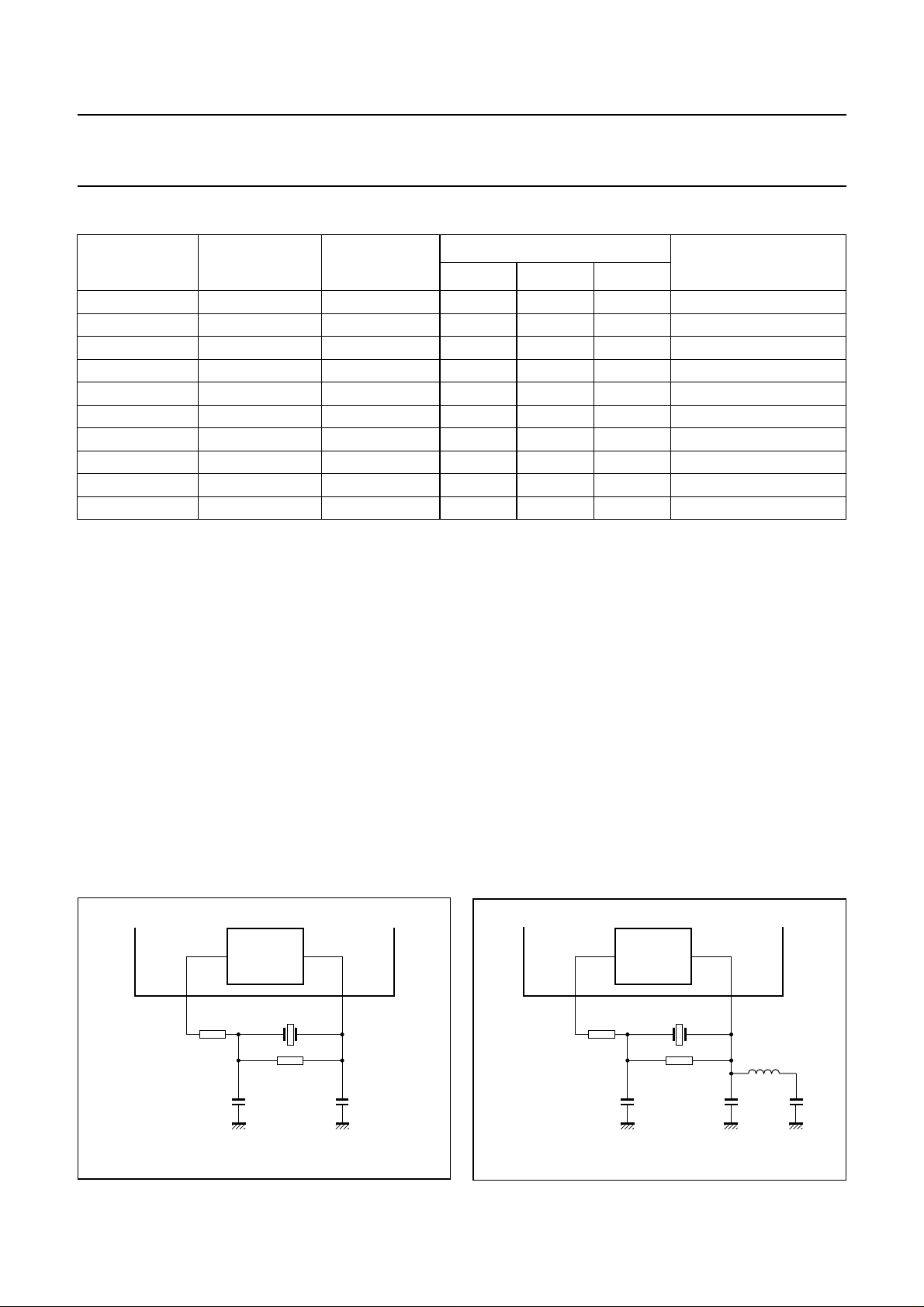
7.2 Crystal oscillator
The crystal oscillator is a conventional 2 pin design
operating between 8 MHz and 35 MHz. This oscillator is
capable of operating with ceramic resonators and with
both fundamental and third overtone crystals. External
components should be used to suppress the fundamental
output of the third overtone crystals as shown in
Figs 3 and 4. Typical oscillation frequencies required are
8.4672, 16.9344 or 33.8688 MHz depending on the
internal clock settings used and whether or not the clock
multiplier is enabled.
SAA7370A
OSCILLATOR
8.4672 MHz
330 Ω
100 kΩ
MBG779
CRINCROUT
22 pF22 pF
SAA7370A
CROUT
MBG778
330 Ω
OSCILLATOR
33.8688 MHz
100 kΩ
CRIN
3.3 µH
1 nF10 pF10 pF
Fig.3 8.4672 MHz fundamental configuration.
1995 Nov 29 9
Fig.4 33.8688 MHz overtone configuration.
Page 10

Philips Semiconductors Preliminary specification
Digital servo processor and Compact Disc
decoder (CD7)
7.3 Data slicer and clock regenerator
The SAA7370A has an integrated slice level comparator
which can be clocked by the crystal frequency clock, or
8 times the crystal frequency clock (if SELPLL is set HIGH
while using an 8.4672 MHz crystal, and register 4 is set
to 0xxx). The slice level is controlled by an internal current
source applied to an external capacitor under the control
of the Digital Phase-Locked Loop (DPLL).
Regeneration of the bit clock is achieved with an internal
fully digital PLL. No external components are required and
the bit clock is not output. The PLL has two registers
(8 and 9) for selecting bandwidth and equalization.
For certain applications an offtrack input is necessary.
This is internally connected from the servo part (its polarity
can be changed by the foc_parm1 parameter), but may be
input via the V1 pin if selected by register C. If this flag is
HIGH, the SAA7370A will assume that its servo part is
following on the wrong track, and will flag all incoming HF
data as incorrect.
SAA7370A
7.4 Demodulator
7.4.1 F
A double timing system is used to protect the demodulator
from erroneous sync patterns in the serial data.
The master counter is only reset if:
• A sync coincidence detected; sync pattern occurs
588 ±1 EFM clocks after the previous sync pattern
• A new sync pattern is detected within ±6 EFM clocks of
its expected position.
The sync coincidence signal is also used to generate the
PLL lock signal, which is active HIGH after 1 sync
coincidence found, and reset LOW if during 61
consecutive frames no sync coincidence is found.
The PLL lock signal can be accessed via the SDA or
STATUS pins selected by register 2 and 7.
Also incorporated in the demodulator is a Run Length 2
(RL2) correction circuit. Every symbol detected as RL2 will
be pushed back to RL3. To do this, the phase error of both
edges of the RL2 symbol are compared and the correction
is executed at the side with the highest error probability.
RAME SYNC PROTECTION
HF
inputs
1 nF
1 nF
22 kΩ
100 nF
V
SSA
22 pF
22 kΩ
100
nF
V
SSA
HFIN
HFREF
I
ref
ISLICE
7.4.2 EFM
DEMODULATION
The 14-bit EFM data and subcode words are decoded into
8-bit symbols.
crystal
clock
DQ
DPLL
1/2V
DD
100 µA
V
SS
V
DD
100 µA
MBG397
Fig.5 Data slicer showing typical application components (for n = 4).
1995 Nov 29 10
Page 11

Philips Semiconductors Preliminary specification
Digital servo processor and Compact Disc
decoder (CD7)
DOBM
SDA
EBU
reg A
INTERFACE
SCLK
WCLK
S-BUS
2
I
1
1
0
1 : no pre-emphasis detected
OR reg D = 01xx (de-emphasis signal at V5)
0 : pre-emphasis detected
AND reg D ≠ 01xx
1
0
DATA
EF
INTERFACE
0
reg 3
(CD-ROM modes)
1 : reg 3 ≠ 101x
0 : reg 3 = 101x
SAA7370A
MBG418
handbook, full pagewidth
V4
1
SBSY
CD GRAPHICS
0
MICROCONTROLLER
SFSY
SUB
INTERFACE
0 : reg D = xx01
V4 SUBCODE
INTERFACE
reg F
INTERFACE
SUBCODE
PROCESSOR
1
0 : reg A = xx1x
1 : reg A = xx0x
DEMODULATOR
DIGITAL PLL AND
mode)
s
(1f
0 : reg 3 ≠ xx10
1 : reg 3 = xx10
0
FIFO
PHASE
COMPENSATION
1
0
FILTER
DIGITAL
FADE/MUTE/
INTERPOLATE
ERROR
CORRECTOR
DE-EMPHASIS
KILL
reg 3
FILTER
V3
KILL
reg C
Fig.6 Simplified data flow of decoder functions.
data slicer
output from
1995 Nov 29 11
Page 12

Philips Semiconductors Preliminary specification
Digital servo processor and Compact Disc
decoder (CD7)
7.5 Subcode data processing
7.5.1 QThe 96-bit Q-channel word is accumulated in an internal
buffer. The last 16 bits are used internally to perform a
Cyclic Redundancy Check (CRC). If the data is good, the
SUBQREADY-I signal will go LOW. SUBQREADY-I can
be read via the SDA or STATUS pins, selected via
register 2. Good Q-channel data may be read from SDA.
7.5.2 EIAJ 3 AND 4-WIRE SUBCODE (CD GRAPHICS)
Data from all the subcode channels (P-to- W) may be read
via the subcode interface, which conforms to
EIAJ CP-2401. The interface is enabled and configured as
either a 3-wire or 4-wire interface via register F.
The subcode interface output formats are illustrated in
Fig.7, where the RCK signal is supplied by another device
such as a CD graphics decoder.
CHANNEL PROCESSING
INTERFACES
SAA7370A
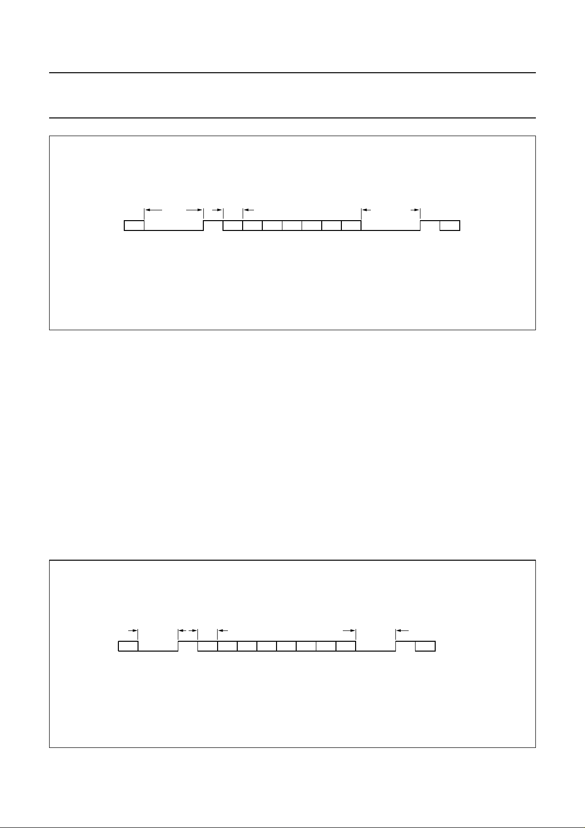
7.5.3 V4
Data of subcode channels, Q-to-W, may be read via pin V4
if selected via register D. The format is similar to RS232
and is illustrated in Fig.8. The subcode sync word is
formed by a pause of (200/n) µs minimum. Each subcode
byte starts with a logic 1 followed by 7 bits (Q-to-W).
The gap between bytes is variable between (11.3/n) µs
and (90/n) µs.
The subcode data is also available in the EBU output
(DOBM) in a similar format.
SUBCODE INTERFACE
handbook, full pagewidth
SBSY
SFSY
RCK
SUB
SFSY
RCK
SUB
SF0 SF1
SF0 SF1 SF2 SF3 SF97 SF0 SF1
SFSY
RCK
SUB
SF2 SF3 SF97 SF0 SF1
P-W P-W P-W
EIAJ 4-wire subcode interface
P-W P-W P-W
EIAJ 3-wire subcode interface
PQRSTUVW
MBG410
Fig.7 EIAJ subcode (CD graphics) interface format.
1995 Nov 29 12
Page 13
Philips Semiconductors Preliminary specification
Digital servo processor and Compact Disc
decoder (CD7)
200/n µs
min
W96 1QRSTUVW 1Q
n =disc speed.
7.6 FIFO and error corrector
The SAA7370A has a ±8 frame FIFO. The error corrector
is a t = 2, e = 4 type, with error corrections on both C1
(32 symbol) and C2 (28 symbol) frames. Four symbols are
used from each frame as parity symbols. This error
corrector can correct up to two errors on the C1 level and
up to four errors on the C2 level.
The error corrector also contains a flag processor. Flags
are assigned to symbols when the error corrector cannot
ascertain if the symbols are definitely good. C1 generates
output flags which are read after (de-interleaving) by C2,
to help in the generation of C2 output flags.
The C2 output flags are used by the interpolator for
concealment of uncorrectable errors. They are also output
via the EBU signal (DOBM) and the EF output with I2S-bus
for CD-ROM applications.
11.3/n
µs
Fig.8 Subcode format and timing on pin V4.
SAA7370A
11.3/n µs min
90/n µs max
MBG401
7.6.1 FLAGS OUTPUT (CFLG)
The flags output pin CFLG (open-drain) shows the status
of the error corrector and interpolator and is updated every
frame (7.35 × n kHz). In the SAA7370A chip a 1-bit flag is
present on the CFLG pin as illustrated in Fig.9. This signal
shows the status of the error corrector and interpolator.
The first flag bit, F1, is the absolute time sync signal, the
FIFO-passed subcode sync and relates the position of the
subcode sync to the audio data (DAC output). This flag
may also be used in a super FIFO or in the synchronization
of different players. The output flags can be made
available at bit 4 of the EBU data format (LSB of the 24-bit
data word), if selected by register A.
handbook, full pagewidth
n = disc speed.
33.9/n µs
11.3/n
µs
F1 F2 F3 F4 F5 F6 F7 F8 F1F8
Fig.9 Flag output timing diagram.
1995 Nov 29 13
33.9/n µs
MBG425
Page 14

Philips Semiconductors Preliminary specification
Digital servo processor and Compact Disc
decoder (CD7)
Table 2 Output flags
F1 F2 F3 F4 F5 F6 F7 F8 DESCRIPTION
0xxxxxxxno absolute time sync
1xxxxxxxabsolute time sync
x00xxxxxC1 frame contained no errors
x01xxxxxC1 frame contained 1 error
x10xxxxxC1 frame contained 2 errors
x11xxxxxC1 frame uncorrectable
x x x 0 0 x x 0 C2 frame contained no errors
x x x 0 0 x x 1 C2 frame contained 1 error
x x x 0 1 x x 0 C2 frame contained 2 errors
x x x 0 1 x x 1 C2 frame contained 3 errors
x x x 1 0 x x 0 C2 frame contained 4 errors
x x x 1 1 x x 1 C2 frame uncorrectable
xxxxx00xno interpolations
xxxxx01xat least one 1-sample interpolation
xxxxx10xat least one hold and no interpolations
xxxxx11xat least one hold and one 1-sample interpolation
SAA7370A
7.6.2 C2FAIL
The C2FAIL pin indicates that invalid data has occurred on
the I2S-bus interface. However, due to the structure of the
corrector it is impossible to determine which byte has
failed. C2FAIL will go LOW for (140/n) µs when invalid
data is detected, this data may then occur (15/n) µs before
or after the pin is activated.
7.7 Audio functions
7.7.1 DE-EMPHASIS AND PHASE LINEARITY
When pre-emphasis is detected in the Q-channel
subcode, the digital filter automatically includes a
de-emphasis filter section. When de-emphasis is not
required, a phase compensation filter section controls the
phase of the digital oversampling filter to ≤±1° within the
band 0 to 16 kHz. With de-emphasis the filter is not phase
linear.
If the de-emphasis signal is set to be available at V5,
selected via register D, then the de-emphasis filter is
bypassed.
7.7.2 D
IGITAL OVERSAMPLING FILTER
These attenuations do not include the sample-and-hold at
the external DAC output or the DAC post filter. When using
the oversampling filter, the output level is scaled −0.5 dB
down, to avoid overflow on full scale sine wave inputs
(0 to 20 kHz).
Table 3 Filter specification
PASS BAND STOP BAND ATTENUATION
0 to 9 kHz −≤0.001 dB
19 to 20 kHz −≤0.03 dB
− 24 kHz ≥25 dB
− 24 to 27 kHz ≥38 dB
− 27 to 35 kHz ≥40 dB
− 35 to 64 kHz ≥50 dB
− 64 to 68 kHz ≥31 dB
− 68 kHz ≥35 dB
− 69 to 88 kHz ≥40 dB
The SAA7370A contains a 2 to 4 times oversampling IIR
filter. The filter specification of the 4 times oversampling
filter is given in Table 3.
1995 Nov 29 14
Page 15

Philips Semiconductors Preliminary specification
Digital servo processor and Compact Disc
decoder (CD7)
7.7.3 CONCEALMENT
A 1 sample linear interpolator becomes active if a single
sample is flagged as erroneous but cannot be corrected.
The erroneous sample is replaced by a level midway
between the preceding and following samples. Left and
right channels have independent interpolators. If more
than one consecutive non-correctable sample is found, the
last good sample is held. A 1-sample linear interpolation is
then performed before the next good sample (see Fig.10).
In CD ROM modes (i.e. the DAC interface is selected to be
in a CD ROM format) concealment is not executed.
7.7.4 M
A digital level controller is present on the SAA7370A which
performs the functions of soft mute, full scale, attenuation
and fade; these are selected via register 0:
Mute: signal reduced to 0 in a maximum of 128 steps;
(3/n) µs.
Attenuate: signal scaled by −12 dB.
Full scale: ramp signal back to 0 dB level. From mute
takes (3/n) µs.
UTE, FULL-SPEED, ATTENUATION AND FADE
SAA7370A
Fade: activates a 128 stage counter which allows the
signal to be scaled up/down by 0.07 dB steps
128 = full scale.
120 = −0.5 dB (i.e. full scale if oversampling filter
used).
32 = −12 dB.
0 = mute.
7.7.5 P
The peak detector measures the highest audio level
(absolute value) on positive peaks for left and right
channels. The 8 most significant bits are output in the
Q-channel data in place of the CRC bits. Bits 81 to 88
contain the left peak value (bit 88 = MSB) and
bits 89 to 96 contain the right peak value (bit 96 = MSB).
The values are reset after reading Q-channel data via
SDA.
EAK DETECTOR
Interpolation Hold Interpolation
OK Error OK Error Error Error OK OK
Fig.10 Concealment mechanism.
1995 Nov 29 15
MGA372
Page 16

Philips Semiconductors Preliminary specification
Digital servo processor and Compact Disc
SAA7370A
decoder (CD7)
7.8 DAC interface
The SAA7370A is compatible with a wide range of digital-to-analog converters (DACs). Eleven formats are supported
and are given in Table 4. Figures 11 and 12 show the Philips I2S-bus and the EIAJ data formats respectively. When the
decoder is operated in lock-to-disc mode, the SCLK frequency is dependent on the disc speed factor ‘d’. All formats are
MSB first and fs is (44.1 × n) kHz. The polarity of the WCLK and the data can be inverted; selectable by register 7.
It should be noted that EF is only a defined output in CD ROM modes.
Table 4 DAC interface formats
REGISTER 3
1010 f
1011 f
1110 f
0010 f
0110 f
0000 4f
0100 4f
1100 4f
0011 2f
0111 2f
1111 2f
SAMPLE
FREQUENCY
s
s
s
s
s
(2)
s
(2)
s
(2)
s
s
s
s
NUMBER OF
BITS
SCLK (MHz) FORMAT INTERPOLATION
16 2.1168 × n CD ROM (I2S-bus) no
16 2.1168 × n CD ROM (EIAJ) no
16/18
(1)
2.1168 × n Philips I2S-bus 16/18 bits
(1)
16 2.1168 × n EIAJ 16 bits yes
18 2.1168 × n EIAJ 18 bits yes
16 8.4672 × n EIAJ 16 bits yes
18 8.4672 × n EIAJ 18 bits yes
18 8.4672 × n Philips I2S-bus 18 bits yes
16 4.2336 × n EIAJ 16 bits yes
18 4.2336 × n EIAJ 18 bits yes
18 4.2336 × n Philips I2S-bus 18 bits yes
yes
Notes
1. in this mode the first 16 bits contain data, but if any of the fade, attenuate or de-emphasis filter functions are activated
then the first 18 bits contain data.
2. Cannot be used in the n = 8 mode.
1995 Nov 29 16
Page 17

Philips Semiconductors Preliminary specification
Digital servo processor and Compact Disc
decoder (CD7)
MBG424
15 1410DATA
01
SAA7370A
MBG423
170DATA
0
S-bus data format (16-bit word length shown).
2
LEFT CHANNEL DATA (WCLK NORMAL POLARITY)
Fig.11 Philips I
SCLK
15 14
LSB error flag MSB error flag LSB error flag MSB error flag
MODES ONLY)
s
EF
(CD-ROM
WCLK
AND If
1995 Nov 29 17
SCLK
LEFT CHANNEL DATA
17
WCLK
EF
MSB error flag LSB error flag MSB error flag
MODES ONLY)
s
(CD-ROM
AND If
Fig.12 EIAJ data format (18-bit word length shown).
Page 18

Philips Semiconductors Preliminary specification
Digital servo processor and Compact Disc
SAA7370A
decoder (CD7)
7.9 EBU interface
The bi-phase mark digital output signal at pin DOBM is in
accordance with the format defined by the IEC958
specification. Three different modes can be selected via
register A;
• DOBM pin held LOW.
• Data taken before concealment, mute and fade (must
always be used for CD ROM modes).
• Data taken after concealment, mute and fade.
Table 5 Format
FUNCTION BITS DESCRIPTION
Sync 0 to 3 −
Auxiliary 4 to 7 not used; normally zero
Error flags 4 CFLG error and interpolation flags when selected by register A
Audio sample 8 to 27 first 4 bits not used (always zero). 2’s compliment. LSB = bit 12, MSB = bit 27
Validity flag 28 valid = logic 0
User data 29 used for subcode data (Q-to-W)
Channel status 30 control bits and category code
Parity bit 31 even parity for bits 4 to 30
7.9.1 FORMAT
The digital audio output consists of 32-bit words
(‘subframes’) transmitted in bi-phase mark code (two
transitions for a logic 1 and one transition for a logic 0).
Words are transmitted in blocks of 384. Table 5 gives the
formats.
Table 6 Description of Table 5
FUNCTION DESCRIPTION
Sync The sync word is formed by violation of the bi-phase rule and therefore does not contain any data.
Its length is equivalent to 4 data bits. The 3 different sync patterns indicate the following situations:
sync B: start of a block (384 words), word contains left sample; sync M: word contains left sample
(no block start) and sync W: word contains right sample.
Audio sample Left and right samples are transmitted alternately.
Validity flag Audio samples are flagged (bit 28 = 1) if an error has been detected but was uncorrectable.
This flag remains the same even if data is taken after concealment.
User data Subcode bits Q-to-W from the subcode section are transmitted via the user data bit.
This data is asynchronous with the block rate.
Channel status The channel status bit is the same for left and right words. Therefore a block of 384 words contains
192 channel status bits. The category code is always CD. The bit assignment is given in Table 7.
1995 Nov 29 18
Page 19

Philips Semiconductors Preliminary specification
Digital servo processor and Compact Disc
SAA7370A
decoder (CD7)
Table 7 Bit assignment
FUNCTION BITS DESCRIPTION
Control 0 to 3 copy of CRC checked Q-channel control bits 0 to 3; bit 2 is logic 1 when copy
permitted; bit 3 is logic 1 when recording has pre-emphasis
Reserved mode 4 to 7 always zero
Category code 8 to 15 CD: bit 8 = logic, all other bits = logic 0
Clock accuracy 28 to 29 set by register A; 10 = level I; 00 = level II; 01 = level III
Remaining 6 to 27 and
30 to 191
7.10 KILL circuit
The KILL circuit detects digital silence by testing for an
all-zero or all-ones data word in the left or right channel
before the digital filter. The output is switched active LOW
when silence has been detected for at least 250 ms, or if
mute is active, or in CD-ROM modes. Two modes are
available which can be selected by register C;
1 pin kill: KILL active LOW indicates silence detected on
both left and right channels.
2 pin kill: KILL active LOW indicates silence detected on
left channel. V3 active LOW indicates silence detected
on right channel.
always zero
7.11 Audio features off
The audio features can be turned off (selected by
register E) which affects the following functions;
• Digital filter, fade, peak detector, KILL circuit (but
outputs KILL, V3 still active) are disabled.
• V5 (if selected to be the de-emphasis flag output) and
the EBU outputs become undefined.
It should be noted that the EBU output should be set LOW
prior to switching the audio features off and after switching
audio features back on a full-scale command should be
given.
It should be noted that when mute is active or in CD-ROM
modes the output(s) are switched LOW.
1995 Nov 29 19
Page 20
Philips Semiconductors Preliminary specification
Digital servo processor and Compact Disc
decoder (CD7)
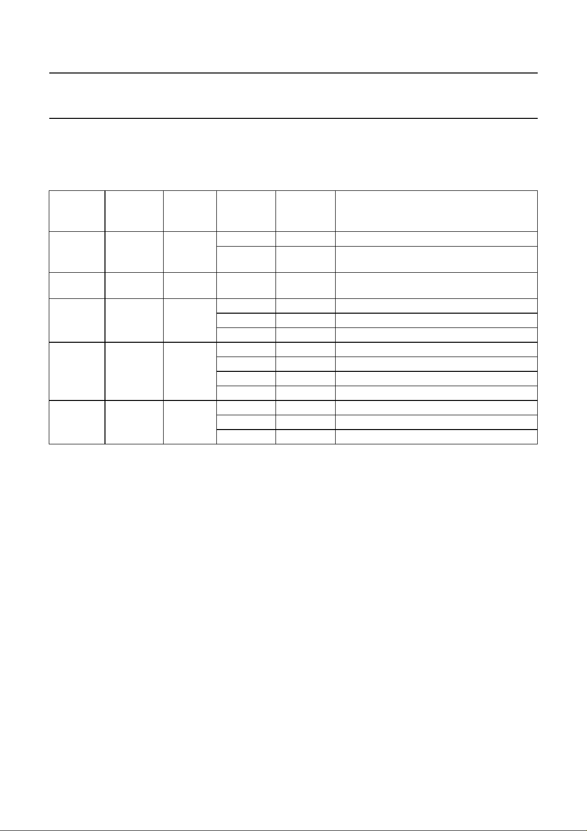
7.12 The VIA interface
The SAA7370A has five pins that can be reconfigured for different applications (see Table 8).
Table 8 Pin applications
PIN NAME
V1 62 input 1100 xxx1 external offtrack signal input
V2 63 input −−input may be read via decoder status bit;
V3 42 output 1100 xx0x KILL output for right channel
V4 41 output 1101 0000 4-line motor drive (using V4 and V5)
V5 40 output 1101 01xx de-emphasis output (active HIGH)
PIN
NUMBER
TYPE
CONTROL
REGISTER
ADDRESS
− xxx0 internal offtrack signal used Input may be read
− x01x output = 0
− x11x output = 1
− xx01 Q-to-W subcode output
− xx10 output = 0
− xx11 output = 1
− 10xx output = 0
− 11xx output = 1
CONTROL
REGISTER
DATA
FUNCTION
via decoder status bit; selected via register 2
selected via register 2
SAA7370A
7.13 Spindle motor control
7.13.1 M
The spindle motor speed is controlled by a fully integrated
digital servo. Address information from the internal
±8 frame FIFO and disc speed information are used to
calculate the motor control output signals. Several output
modes, selected by register 6, are supported:
• Pulse density, 2-line (true complement output),
(1 × n) MHz sample frequency
• PWM output, 2-line, (22.05 × n) kHz modulation
frequency
• PWM output, 4-line, (22.05 × n) kHz modulation
frequency
• CDV motor mode.
OTOR OUTPUT MODES
7.13.1.1 Pulse density output mode
In the pulse density mode the motor output pin (MOTO1)
is the pulse density modulated motor output signal. A 50%
duty factor corresponds with the motor not actuated,
higher duty factors mean acceleration, lower mean
braking. In this mode, the MOTO2 signal is the inverse of
the MOTO1 signal. Both signals change state only on the
edges of a (1 × n) MHz internal clock signal. Possible
application diagrams are illustrated in Fig.13.
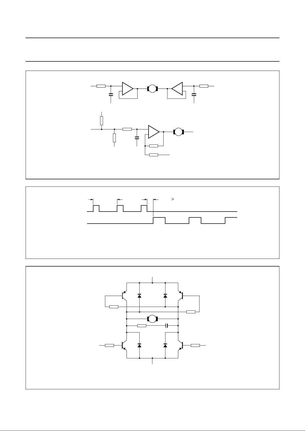
7.13.1.2 PWM output mode (2-line)
In the PWM mode the motor acceleration signal is put in
pulse-width modulation form on the MOTO1 output.
The motor braking signal is pulse-width modulated on the
MOTO2 output. The timing is illustrated in Fig.14. A typical
application diagram is illustrated in Fig.15.
1995 Nov 29 20
Page 21
Philips Semiconductors Preliminary specification
Digital servo processor and Compact Disc
decoder (CD7)
22 kΩ
22 kΩ
10 nF
V
DD
V
SS
+
–
22 kΩ
M
+
SS
–
22 kΩ
22 kΩ
22 kΩ
10 nF
V
SS
V
Fig.13 Motor pulse density application diagrams.
MOTO1
MOTO1
SAA7370A
+
22 kΩ
–
M
V
DD
10 nF
V
SS
V
SS
MOTO2
MGA363 - 1
t 240 ns
dead
MOTO1
MOTO2
t = 45 µs
rep
Accelerate Brake
Fig.14 2-line PWM mode timing.
+
M
10 Ω
MOTO1 MOTO2
100 nF
MGA366
V
Fig.15 Motor 2-line PWM mode application diagram.
1995 Nov 29 21
SS
MGA365 - 2
Page 22
Philips Semiconductors Preliminary specification
Digital servo processor and Compact Disc
SAA7370A
decoder (CD7)
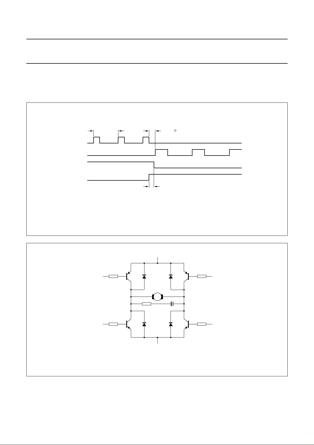
7.13.1.3 PWM output mode (4-line)
Using two extra outputs from the versatile pins Interface, it is possible to use the SAA7370A with a 4-input motor bridge.
The timing is illustrated in Fig.16. A typical application diagram is illustrated in Fig.17.
t = 45 µs t 240 ns
rep
MOTO1
MOTO2
V4
V5
Accelerate Brake
dead
t = 240 ns
ovl
MGA367 - 1
Fig.16 4-line PWM mode timing.
+
V4
M
10 Ω
MOTO1
100 nF
V
SS
Fig.17 Motor 4-line PWM mode application diagram.
V5
MOTO2
MGA364 - 2
1995 Nov 29 22
Page 23

Philips Semiconductors Preliminary specification
Digital servo processor and Compact Disc
decoder (CD7)
7.13.1.4 CDV/CAV output mode
In the CDV motor mode, the FIFO position will be put in
pulse-width modulated form on the MOTO1 pin [carrier
frequency (300 × d) Hz], where ‘d’ is the disc speed factor.
The PLL frequency signal will be put in pulse-density
modulated form (carrier frequency 4.23 × n MHz) on the
MOTO2 pin. The integrated motor servo is disabled in this
mode.
The PWM signal on MOTO1 corresponds to a total
memory space of 20 frames, therefore the nominal FIFO
position (half full) will result in a PWM output of 60%.
In the lock to-disc (CAV) mode the CDV motor mode is the
only mode that can be used to control the motor.
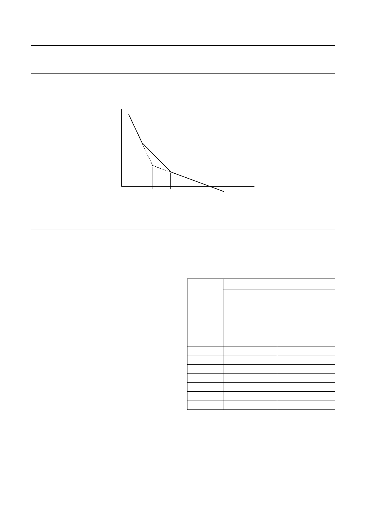
7.13.2 S
The operation modes of the motor servo is controlled by
register 1 (see Table 9).
In the SAA7370A decoder there is an anti-windup mode for
the motor servo, selected via register 1. When the
anti-wind-up mode is activated the motor servo integrator
will hold if the motor output saturates.
7.13.2.1 Power limit
In start mode 1, start mode 2, stop mode 1 and stop
mode 2, a fixed positive or negative voltage is applied to
the motor.
PINDLE MOTOR OPERATING MODES
SAA7370A
This voltage can be programmed as a percentage of the
maximum possible voltage, via register 6, to limit current
drain during start and stop.
The following power limits are possible;
100% (no power limit), 75%, 50%, or 37% of maximum.
7.13.3 L
The gain and crossover frequencies of the motor control
loop can be programmed via registers 4 and 5.
The following parameter values are possible;
Gains: 3.2, 4.0, 6.4, 8.0, 12.8, 16, 25.6 and 32
Crossover frequency f4: 0.5 × n Hz, 0.7 × n Hz,
1.4 × n Hz, 2.8 × nHz
Crossover frequency f3: 0.85 × n Hz, 1.71 × n Hz,
3.42 × nHz
It should be noted that the crossover frequencies f3 and f
are scaled with the overspeed factor ‘n’ whereas the gains
are not.
7.13.4 FIFO
If FIFO overflow occurs during Play mode (e.g.: as a result
of motor rotational shock), the FIFO will be automatically
reset to 50% and the audio interpolator tries to conceal as
much as possible to minimise the effect of data loss.
OOP CHARACTERISTICS
OVERFLOW
4
Table 9 Operating modes
MODE DESCRIPTION
Start mode 1 The disc is accelerated by applying a positive voltage to the spindle motor. No decisions are
involved and the PLL is reset. No disc speed information is available for the microcontroller.
Start mode 2 The disc is accelerated as in start mode 1, however the PLL will monitor the disc speed. When the
disc reaches 75% of its nominal speed, the controller will switch to jump mode. The motor status
signals selectable via register 2 are valid.
Jump mode Motor servo enabled but FIFO kept reset at 50%, integrator is held. The audio is muted but it is
possible to read the subcode. It should be noted that in the CD-ROM modes the data, on EBU and
the I2S-bus is not muted.
Jump mode 1 Similar to jump mode but motor integrator is kept at zero. Used for long jumps where there is a large
change in disc speed.
Play mode FIFO released after resetting to 50%. Audio mute released.
Stop mode 1 Disc is braked by applying a negative voltage to the motor. No decisions are involved.
Stop mode 2 The disc is braked as in stop mode 1 but the PLL will monitor the disc speed. As soon as the disc
reaches 12% (or 6%, depending on the programmed brake percentage, via register E) of its
nominal speed, the MOTSTOP status signal will go HIGH and switch the motor servo to Off mode.
Off mode Motor not steered.
1995 Nov 29 23
Page 24
Philips Semiconductors Preliminary specification
Digital servo processor and Compact Disc
decoder (CD7)
G
fBW
f
4
3
Fig.18 Motor servo mode diagram.
SAA7370A
MGA362 - 2
f
7.14 Servo part
7.14.1 D
IODE SIGNAL PROCESSING
The photo detector in conventional two-stage three-beam
compact disc systems normally contains six discrete
diodes. Four of these diodes (three for single foucault
systems) carry the central aperture signal (CA) while the
other two diodes (satellite diodes) carry the radial tracking
information. The CA signal is processed into an HF signal
(for the decoder function) and LF signal (information for the
focus servo loop) before it is supplied to the SAA7370A.
The analog signals from the central and satellite diodes
are converted into a digital representation using
analog-to-digital converters (ADCs). The ADCs are
designed to convert unipolar currents into a digital code.
The dynamic range of the input currents is adjustable
within a given range, which is dependent on the value of
external resistor connected to pin I
. The maximum
refT
current for the central diodes and satellite diodes is given
in the following formulae;
2.4 106–×
I
in max central,()
=
-------------------------R
IrefT
µA
current generated by the external resistor on I
application VRL is connected to V
. The maximum input
SSA1
refT
currents for a range of resistors is given Table 10.
Table 10 Maximum current input
DIODE INPUT CURRENT RANGE
R
(kΩ)
IrefT
D1 to D4 (µA) R1 and R2 (µA)
220 10.909 5.455
240 10.000 5.000
270 8.889 4.444
300 8.000 4.000
330 7.273 3.636
360 6.667 3.333
390 6.154 3.077
430 5.581 2.791
470 5.106 2.553
510 4.706 2.353
560 4.286 2.143
620 3.871 1.935
. In the
1.2 106–×
I
in max satellite,()
=
-------------------------R
IrefT
µA
The VRH voltage is internally generated by control circuitry
which ensures that the VRH voltage is adjusted depending
on the spread of internal capacitors, using the reference
1995 Nov 29 24
This mode of V
automatic adjustment can be selected
RH
by the preset latch command.
Alternatively, the dynamic range of the input currents can
be made dependent on the ADC reference voltages VRL
and VRH. The maximum current for the central diodes and
satellite diodes is given in the following formulae;
Page 25

Philips Semiconductors Preliminary specification
Digital servo processor and Compact Disc
decoder (CD7)
I
in max central,()
I
in max satellite,()
where f
= 4.2336 MHz.
sys
f
VRHVRL–()1.0 106–×××=
sys
f
sys
V
–()1.0 106–×××=
RHVRL
VRH is generated internally, and there are 32 levels which
can be selected under software control via the preset latch
command. With this command the VRH voltage can be set
to 2.5 V then modified, decremented one level or
incremented, by resending the command the required
number of times. In the application VRL is connected to
V
.
SSA1
7.14.2 S
IGNAL CONDITIONING
The digital codes retrieved from the ADCs are applied to
logic circuitry to obtain the various control signals.
The signals from the central aperture diodes are
processed to obtain a normalised focus error signal.
FE
n
D1 D2–
---------------------D1 D2+
D3 D4–
–=
---------------------D3 D4+
where the detector set-up is assumed as shown in Fig.19.
µA
µA
SAA7370A
The error signal, FE
proportional integral and differential (PID) filter section.
A Focus OK (FOK) flag is generated by means of the
central aperture signal and an adjustable reference level.
This signal is used to provide extra protection for the
track-loss (TL) generation, the focus start-up procedure
and the drop out detection.
The radial or tracking error signal is generated by the
satellite detector signals R1 and R2. The radial error signal
can be formulated as follows:
RE
R1 R2–()re_gain R1 R2–()re_gain×+×=
s
where the index ‘s’ indicates the automatic scaling
operation which is performed on the radial error signal.
This scaling is necessary to avoid non-optimum dynamic
range usage in the digital representation and reduces the
radial bandwidth spread. Furthermore, the radial error
signal will be made free from offset during start up of the
disc.
The four signals from the central aperture detectors,
together with the satellite detector signals generate a track
position signal (TPI) which can be formulated as follows:
, is further processed by a
n
In the event of single Foucault focusing method, the signal
conditioning can be switched under software control such
that the signal processing is as follows:
D1 D2–
2
FE
handbook, full pagewidth
×=
n
---------------------D1 D2+
SATELLITE
DIODE R1
D1
D3
D2
SATELLITE
DIODE R2
single Foucault astigmatic focus double Foucault
TPI = sign [(D1 + D2 + D3 + D4) − (R1 + R2) × sum_gain
where the weighting factor sum_gain is generated
internally by the SAA7370A during initialization.
SATELLITE
DIODE R1
D1
D2
D3
D4
SATELLITE
DIODE R2
SATELLITE
DIODE R1
D1
D2
D3
D4
SATELLITE
DIODE R2
MBG422
Fig.19 Detector arrangement.
1995 Nov 29 25
Page 26

Philips Semiconductors Preliminary specification
Digital servo processor and Compact Disc
decoder (CD7)
7.14.3 FOCUS SERVO SYSTEM
7.14.3.1 Focus start-up
Five initially loaded coefficients influence the start-up
behaviour of the focus controller. The automatically
generated triangle voltage can be influenced by
3 parameters; for height (ramp_height) and DC offset
(ramp_offset) of the triangle and its steepness
(ramp_incr).
For protection against false focus point detections two
parameters are available which are an absolute level on
the CA-signal (CA_start) and a level on the FEn signal
(FE_start). When this CA level is reached the FOK signal
becomes true.
If the FOK signal is true and the level on the FEn signal is
reached, the focus PID is enabled to switch on when the
next zero crossing is detected in the FEn signal.
7.14.3.2 Focus position control loop
The focus control loop contains a digital PID controller
which has 5 parameters which are available to the user.
These coefficients influence the integrating (foc_int),
proportional (foc_lead_length, part of foc_parm3) and
differentiating (foc_pole_lead, part of foc_parm1) action of
the PID and a digital low-pass filter (foc_pole_noise, part
of foc_parm2) following the PID. The fifth coefficient
foc_gain influences the loop gain.
7.14.3.3 Drop-out detection
This detector can be influenced by one parameter
(CA_drop). The FOK signal will become false and the
integrator of the PID will hold if the CA signal drops below
this programmable absolute CA level. When the FOK
signal becomes false it is assumed, initially, to be caused
by a black dot.
SAA7370A
action of the PID can be switched at the same time as the
gain switching is performed.
7.14.3.6 Focus automatic gain control loop
The loop gain of the focus control loop can be corrected
automatically to eliminate tolerances in the focus loop.
This gain control injects a signal into the loop which is used
to correct the loop gain. Since this decreases the optimum
performance, the gain control should only be activated for
a short time (for example, when starting a new disc).
7.14.4 R
7.14.4.1 Level initialization
During start-up an automatic adjustment procedure is
activated to set the values of the radial error gain (re_gain),
offset (re_offset) and satellite sum gain (sum_gain) for TPI
level generation. The initialization procedure runs in a
radial open loop situation and is ≤300 ms. This start-up
time period may coincide with the last part of the motor
start-up time period.
Automatic gain adjustment: as a result of this
initialization the amplitude of the RE signal is adjusted to
within ±10% around the nominal RE amplitude.
Offset adjustment: the additional offset in RE due to the
limited accuracy of the start-up procedure is less than
±50 nm.
TPI level generation: the accuracy of the initialization
procedure is such that the duty factor range of TPI
becomes 0.4 < duty factor < 0.6 (default duty
factor = TPI HIGH/TPI period).
7.14.4.2 Sledge control
The microcontroller can move the sledge in both directions
via the steer sledge command.
ADIAL SERVO SYSTEM
7.14.3.4 Focus loss detection and fast restart
Whenever FOK is false for longer than approximately
3 ms, it is assumed that the focus point is lost. A fast
restart procedure is initiated which is capable of restarting
the focus loop within 200 to 300 ms depending on the
programmed coefficients of the microcontroller.
7.14.3.5 Focus loop gain switching
The gain of the focus control loop (foc_gain) can be
multiplied by a factor of 2 or divided by a factor of 2 during
normal operation. The integrator value of the PID is
corrected accordingly. The differentiating (foc_pole_lead)
1995 Nov 29 26
7.14.4.3 Tracking control
The actuator is controlled using a PID loop filter with user
defined coefficients and gain. For stable operation
between the tracks, the S-curve is extended over 0.75 of
the track. On request from the microcontroller, S-curve
extension over 2.25 tracks is used, automatically changing
to access control when exceeding those 2.25 tracks.
Both modes of S-curve extension make use of a
track-count mechanism. In this mode, track counting
results in an ‘automatic return-to-zero track’, to avoid
major music rhythm disturbances in the audio output for
improved shock resistance.
The sledge is continuously controlled, or provided with
Page 27

Philips Semiconductors Preliminary specification
Digital servo processor and Compact Disc
decoder (CD7)
step pulses to reduce power consumption using the
filtered value of the radial PID output. Alternatively, the
microcontroller can read the average voltage on the radial
actuator and provide the sledge with step pulses to reduce
power consumption. Filter coefficients of the continuous
sledge control can be preset by the user.
7.14.4.4 Access
The access procedure is divided into two different modes
(see Table 11), depending on the requested jump size.
Table 11 Access modes
ACCESS
TYPE
Actuator jump 1 - brake_distance decreasing
Sledge jump brake_distance - 32768 maximum
Note
1. Microcontroller presettable.
The access procedure makes use of a track counting
mechanism, a velocity signal based on a fixed number of
tracks passed within a fixed time interval, a velocity set
point calculated from the number of tracks to go and a user
programmable parameter indicating the maximum sledge
performance.
If the number of tracks remaining is greater than the
brake_distance then the sledge jump mode should be
activated or, the actuator jump should be performed.
The requested jump size together with the required sledge
breaking distance at maximum access speed defines the
brake_distance value.
During the actuator jump mode, velocity control with a PI
controller is used for the actuator. The sledge is then
continuously controlled using the filtered value of the radial
PID output. All filter parameters (for actuator and sledge)
are user programmable.
In the sledge jump mode maximum power (user
programmable) is applied to the sledge in the correct
direction while the actuator becomes idle (the contents of
the actuator integrator leaks to zero just after the sledge
jump mode is initiated). The actuator can be electronically
damped during sledge jump. The gain of the damping loop
is controlled via the hold_mult parameter.
JUMP SIZE
(1)
ACCESS
SPEED
velocity
power to
(1)
sledge
SAA7370A
Fast track jumping circuitry can be enabled/disabled via
the xtra_preset parameter.
7.14.4.5 Radial automatic gain control loop
The loop gain of the radial control loop can be corrected
automatically to eliminate tolerances in the radial loop.
This gain control injects a signal into the loop which is used
to correct the loop gain. Since this decreases the optimum
performance, the gain control should only be activated for
a short time (for example, when starting a new disc).
This gain control differs from the level initialization.
The level initialization should be performed first.
The disadvantage of using the level initialization without
the gain control is that only tolerances from the front-end
are reduced.
7.14.5 O
The track position signal (TPI) is a flag which is used to
indicate whether the radial spot is positioned on the track,
with a margin of ±1⁄4 of the track-pitch. In combination with
the radial polarity flag (RP) the relative spot position over
the tracks can be determined. These signals are, however,
afflicted with some uncertainties caused by;
• Disc defects such as scratches and fingerprints
• The HF information on the disc, which is considered as
noise by the detector signals.
In order to determine the spot position with sufficient
accuracy, extra conditions are necessary to generate a
track loss signal (TL) and an off-track counter value. These
extra conditions influence the maximum speed and this
implies that, internally, one of the following three counting
states is selected;
1. Protected state: used in normal play situations. A good
2. Slow counting state: used in low velocity track jump
3. Fast counting state: used in high velocity track jump
FF-TRACK COUNTING
protection against false detection caused by disc
defects is important in this state.
situations. In this state a fast response is important
rather than the protection against disc defects (if the
phase relationship between TL and RP of1⁄2πradians
is affected too much, the direction cannot then be
determined accurately).
situations. Highest obtainable velocity is the most
important feature in this state.
1995 Nov 29 27
Page 28

Philips Semiconductors Preliminary specification
Digital servo processor and Compact Disc
decoder (CD7)
7.14.6 DEFECT DETECTION
handbook, full pagewidth
sat1
sat2
+
−
A defect detection circuit is incorporated into the
SAA7370A. If a defect is detected, the radial and focus
error signals may be zeroed, resulting in better playability.
The defect detector can be switched off, applied only to
focus control or applied to both focus and radial controls
under software control (part of foc_parm1).
The defect detector (see Fig.20) has programmable set
points selectable by the parameter defect_parm.
7.14.7 O
FF-TRACK DETECTION
During active radial tracking, off-track detection has been
realised by continuously monitoring the off-track counter
value. The off-track flag becomes valid whenever the
off-track counter value is not equal to zero. Depending on
the type of extended S-curve, the off-track counter is reset
after 0.75 extend or at the original track in the 2.25 track
extend mode.
DECIMATION
FILTER
FAST
FILTER
SLOW
FILTER
Fig.20 Block diagram of defect detector.
SAA7370A
DEFECT
GENERATION
PROGRAMMABLE
HOLD-OFF
been crossed during time defined by jumpwatchtime
parameter.
6. Autosequencer state change.
7. Autosequencer error.
8. Subcode interface blocked: the internal decoder
interface is being used.
It should be noted that if the STATUS pin output is selected
via register 2 and either the microcontroller writes a
different value to register 2 or the decoder interface is
enabled then the STATUS output will change.
7.14.8.2 Decoder interface
The decoder interface allows registers 0 to F to be
programmed and subcode Q-channel data to be read via
servo commands. The interface is enabled/disabled by the
preset latch command (and the xtra_preset parameter).
defect
output
MBG421
7.14.8 H
IGH-LEVEL FEATURES
7.14.8.1 Interrupt mechanism and STATUS pin
The STATUS pin is an output which is active LOW, its
output is selected by register 7 to be either the status bit
(active LOW) selected by register 2 (only available in
4-wire bus mode) or the interrupt signal generated by the
servo part.
8 signals from the interrupt status register are selectable
from the servo part via the interrupt_mask parameter.
The interrupt is reset by sending the read high-level status
command. The 8 signals are as follows;
1. Focus lost: drop out of longer than 3 ms.
2. Subcode ready.
3. Subcode absolute seconds changed.
4. Subcode discontinuity detected: new subcode time
before previous subcode time, or more than 10 frames
later than previous subcode time.
5. Radial error: during radial on-track, no new subcode
frame occurs within time defined by playwatchtime
parameter. During radial jump, less than 4 tracks have
1995 Nov 29 28
7.14.8.3 Automatic error handling
Three watchdogs are present:
1. Focus: detects focus drop out of longer than 3 ms, sets
focus lost interrupt, switches off radial and sledge
servos, disables drive to disc motor.
2. Radial play: started when radial servo is on-track
mode and a first subcode frame is found. Detects
when maximum time between two subcode frames
exceeds time set by playwatchtime parameter; then
sets radial error interrupt, switches radial and sledge
servos off, puts disc motor in jump mode.
3. Radial jump: active when radial servo in long jump or
short jump modes. Detects when the off-track counter
value decreases by less than 4 tracks between two
readings (time interval set by jumpwatchtime
parameter); then sets radial jump error, switches radial
and sledge servos off to cancel jump.
The focus watchdog is always active, the radial watchdogs
are selectable via the radcontrol parameter.
Page 29

Philips Semiconductors Preliminary specification
Digital servo processor and Compact Disc
decoder (CD7)
7.14.8.4 Automatic sequencers and timer interrupts
Two automatic sequencers are implemented (and must be
initialized after power-on);
1. Autostart sequencer: controls the start-up of focus,
radial and motor.
2. Autostop sequencer: brakes the disc and shuts down
servos.
When the automatic sequencers are not used it is possible
to generate timer interrupts, defined by the
time_parameter coefficient.
7.14.8.5 High-level status
The read high-level status command can be used to obtain
the interrupt, decoder, autosequencer status registers and
the motor start time. Use of the read high-level status
command clears the interrupt status register, and
re-enables the subcode read via a servo command.
7.14.9 D
The control signals (pins RA, FO and SL) for the
mechanism actuators are pulse density modulated.
The modulating frequency can be set to either 1.0584 MHz
(DSD mode) or 2.1168 MHz; controlled via the xtra_preset
parameter (it should be noted that these frequencies are
doubled if a 16.9344 MHz crystal is used with
SELPLL = 1). An analog representation of the output
signals can be achieved by connecting a first-order
low-pass filter to the outputs.
RIVER INTERFACE
SAA7370A
During reset (i.e. RESET pin is held LOW) the RA, FO and
SL pins are high-impedance.
7.14.10 LASER INTERFACE
The LDON pin (open-drain output) is used to switch the
laser off and on. When the laser is on the output is
high-impedance. The action of the LDON pin is controlled
by the xtra_preset parameter; the pin is automatically
driven if the focus control loop is active.
7.14.11 R
The shock detector (see Fig.21) can be switched on during
normal track following, and detects within an adjustable
frequency whether disturbances in the radial spot position
relative to the track exceed an adjustable level (controlled
by shock_level). Every time the radial tracking error (RE)
exceeds this level the radial control bandwidth is switched
to twice its original bandwidth and the loop gain is
increased by a factor of 4.
The shock detection level is adjustable in 16 steps from
0 to 100% of the traverse radial amplitude which is sent to
an amplitude detection unit via an adjustable band-pass
filter (controlled by sledge_parm1); lower corner frequency
can be set at either 0 or 20 Hz, and upper corner
frequency at 750 or 1850 Hz. The shock detector is
switched off automatically during jump mode.
ADIAL SHOCK DETECTOR
handbook, full pagewidth
RE
HIGH-PASS FILTER
(0 or 20 Hz)
LOW-PASS FILTER
(750 or 1850 Hz)
Fig.21 Block diagram of radial shock detector.
1995 Nov 29 29
AMPLITUDE
DETECTION
SHOCK
OUTPUT
MGC914
Page 30

Philips Semiconductors Preliminary specification
Digital servo processor and Compact Disc
decoder (CD7)
7.15 Microcontroller interface
Communication on the microcontroller interface can be
set-up in two different modes;
1. 4-wire bus mode: protocol compatible with SAA7345
(CD6) and TDA1301 (DSIC2) where;
a) SCL = serial bit clock.
b) SDA = serial data.
c) RAB = R/W control and data strobe (active HIGH)
for writing to registers 0 to F, reading status bit
selected via register 2 and reading Q-channel
subcode.
d) SILD = R/W control and data strobe (active LOW)
for servo commands.
2. I2C-bus mode: I2C-bus protocol where SAA7370A
behaves as slave device, activated by setting
RAB = HIGH and SILD = LOW where;
a) I2C-bus slave address (write mode) = 30H.
b) I2C-bus slave address (read mode) = 31H.
c) Maximum data transfer rate = 400 kbits/s.
SAA7370A
MOTSTART1: HIGH if motor is turning at 75% or more
of nominal speed.
MOTSTART2: HIGH if motor is turning at 50% or more
of nominal speed.
MOTSTOP: HIGH if motor is turning at 12% or less of
nominal speed. Can be set to indicate 6% or less
(instead of 12% or less) via register E.
PLL Lock: HIGH if sync coincidence signals are found.
V1: follows input on V1 pin.
V2: follows input on V2 pin.
MOTOR-OV: HIGH if the motor servo output stage
saturates.
FIFO-OV: HIGH if FIFO overflows.
SHOCK:
FIFO-OV + servo interrupt signal + OTD (HIGH if shock
detected).
LA-SHOCK: latched SHOCK signal.
The status read protocol is shown in Fig.24. It should be
noted that SILD must be held HIGH.
MOTSTART2 + PLL Lock + MOTOR-OV +
It should be noted that only servo commands can be used
therefore, writing to registers 0 to F, reading decoder
status and reading Q-channel subcode data must be
performed by servo commands.
7.15.1 M
ICROCONTROLLER INTERFACE (4-WIRE BUS MODE)
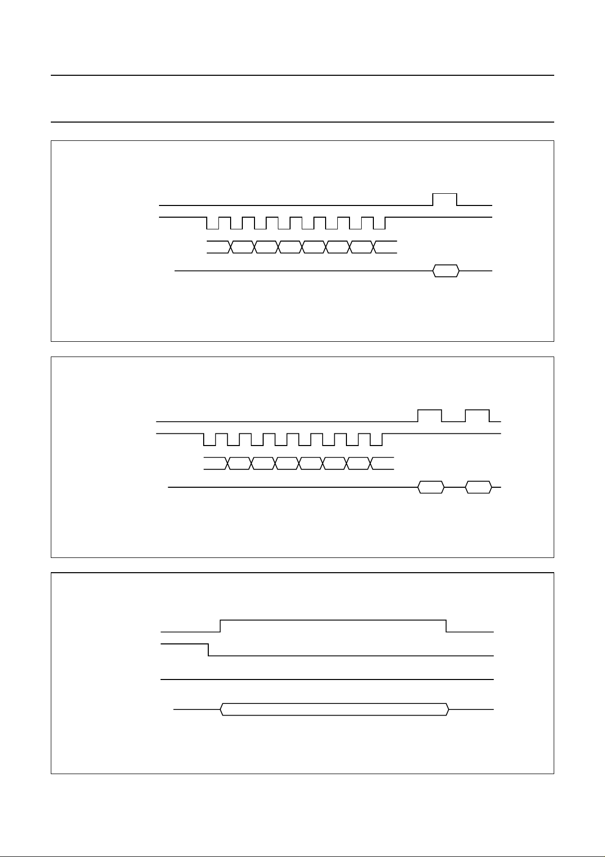
7.15.1.1 Writing data to registers 0 to F
The sixteen 4-bit programmable configuration registers,
0 to F (see Table 12), can be written to via the
microcontroller interface using the protocol shown in
Fig.22.
It should be noted that SILD must be held HIGH; A3 to A0
identifies the register number and D3 to D0 is the data; the
data is latched into the register on the LOW-to-HIGH
transition of RAB.
7.15.1.2 Writing repeated data to registers 0 to F
The same data can be repeated several times (e.g. for a
fade function) by applying extra RAB pulses as shown in
Fig.23. It should be noted that SCL must stay HIGH
between RAB pulses.
7.15.1.3 Reading decoder status information on SDA
There are several internal status signals, selected via
register 2, which can be made available on the SDA line;
SUBQREADY-I: LOW if new subcode word is ready in
Q-channel register.
7.15.1.4 Reading Q-channel subcode
To read the Q-channel subcode direct in the 4-wire bus
mode, the SUBQREADY-I signal should be selected as
status signal. The subcode read protocol is illustrated in
Fig.25.
It should be noted that SILD must be held HIGH; after
subcode read starts, the microcontroller may take as long
as it wants to terminate the read operation; when enough
subcode has been read (1 to 96 bits), terminate reading by
pulling RAB LOW.
Alternatively, the Q-channel subcode can be read using a
servo command as follows:
• Use the read high-level status command to monitor the
subcode ready signal.
• Send the read subcode command, and read the
required number of bytes (up to 12).
• Send the read high-level status command; to re-enable
the decoder interface.
7.15.1.5 Behaviour of the SUBQREADY-I signal
When the CRC of the Q-channel word is good, and no
subcode is being read, the SUBQREADY-I status signal
will react as shown in Fig.26. When the CRC is good and
the subcode is being read, the timing in Fig.27 applies.
1995 Nov 29 30
Page 31

Philips Semiconductors Preliminary specification
Digital servo processor and Compact Disc
decoder (CD7)
If t1 (SUBQREADY-I status LOW to end of subcode read)
is below 2.6/n ms, then t2= 13.1/n ms (i.e.: the
microcontroller can read all subcode frames if it completes
the read operation within 2.6/n ms after the subcode is
ready). If this criterion is not met, it is only possible to
guarantee that t3 will be below 26.2/n ms (approximately).
If subcode frames with failed CRCs are present, the t2 and
t3 times will be increased by 13.1/n ms for each defective
subcode frame.
It should be noted that in the lock-to-disc mode ‘n’ is
replaced by ‘d’, which is the disc speed factor.
7.15.1.6 Write servo commands
A write data command is used to transfer data (a number
of bytes) from the microcontroller, using the protocol
shown in Fig.28. The first of these bytes is the command
byte and the following are data bytes; the number
(between 1 and 7) depends on the command byte.
It should be noted that RAB must be held LOW; the
command or data is interpreted by the SAA7370A after the
HIGH-to-LOW transition of SILD; there must be a
minimum time of 70 µs between SILD pulses.
7.15.1.7 Writing repeated data in servo commands
The same data byte can be repeated by applying extra
SILD pulses as illustrated in Fig.29. SCL must be HIGH
between the SILD pulses.
7.15.1.8 Read servo commands
SAA7370A
The sequence for a write data command (that requires
3 data bytes) is as follows;
• Send START condition
• Send address 30H (write)
• Write command byte
• Write data byte 1
• Write data byte 2.
• Write data byte 3
• Send STOP condition.
It should be noted that more than one command can be
sent in one write sequence.
The sequence for a read data command (that reads 2 data
bytes) is as follows;
• Send START condition
• Send address 30H (write)
• Write command byte
• Send STOP condition.
• Send START condition
• Send address 31H (read)
• Read data byte 1
• Read data byte 2
• Send STOP condition.
It should be noted that the timing constraints specified for
the read and write servo commands must still be adhered
to.
A read data command is used to transfer data (status
information) to the microcontroller, using the protocol
shown in Fig.30. The first byte written determines the type
of command. After this byte a variable number of bytes can
be read. It should be noted that RAB must be held LOW;
after the end of the command byte (LOW-to-HIGH
transition on SILD) there must be a delay of 70 µs before
reading data is started (i.e. the next HIGH-to-LOW
transition on SILD); there must be a minimum time of 70 µs
between SILD pulses.
7.15.2 M
Bytes are transferred over the interface in groups
(i.e. servo commands) of which there are two types:
write data commands and read data commands.
1995 Nov 29 31
ICROCONTROLLER INTERFACE (I
2
C-BUS MODE)
Page 32
Philips Semiconductors Preliminary specification
Digital servo processor and Compact Disc
decoder (CD7)
RAB
(microcontroller)
SCL
(microcontroller)
SDA
(microcontroller)
SDA
(SAA7370A)
Fig.22 Microcontroller write protocol for registers 0 to F.
A3 A2 A1 A0 D3 D2 D1 D0
high-impedance
SAA7370A
MBG769
RAB
(microcontroller)
SCL
(microcontroller)
SDA
(microcontroller)
SDA
(SAA7370A)
RAB
(microcontroller)
SCL
(microcontroller)
SDA
(microcontroller)
SDA
(SAA7370A)
A3 A2 A1 A0 D3 D2 D1 D0
high-impedance
MBG768
Fig.23 Microcontroller write protocol for registers 0 to F (repeat mode).
high-impedance
STATUS
MBG770
Fig.24 Microcontroller read protocol for decoder status on SDA.
1995 Nov 29 32
Page 33
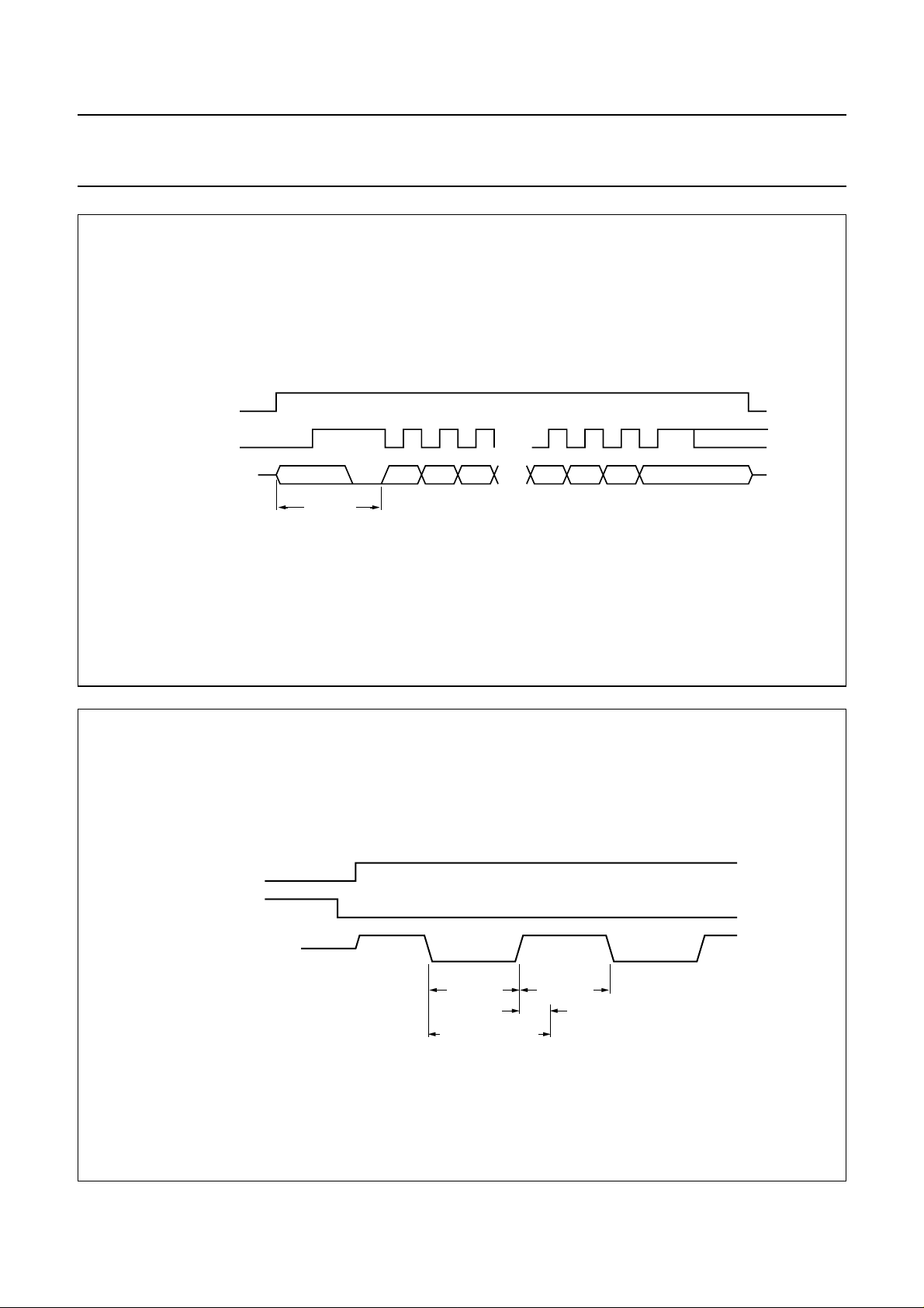
Philips Semiconductors Preliminary specification
Digital servo processor and Compact Disc
decoder (CD7)
RAB
(microcontroller)
SCL
(microcontroller)
SDA
(SAA7370A)
STATUS
CRC
OK
Q1 Q2 Q3 Qn–1
SAA7370A
Qn–2 Qn
MBG771
RAB
(microcontroller)
SCL
(microcontroller)
SDA
(SAA7370A)
Fig.25 Microcontroller protocol for reading Q-channel subcode.
high
impedance
CRC OK CRC OK
10.8/n ms 15.4/n ms
READ start allowed
2.3/n
ms
MBG772
Fig.26 SUBQREADY-I status timing when no subcode is read.
1995 Nov 29 33
Page 34
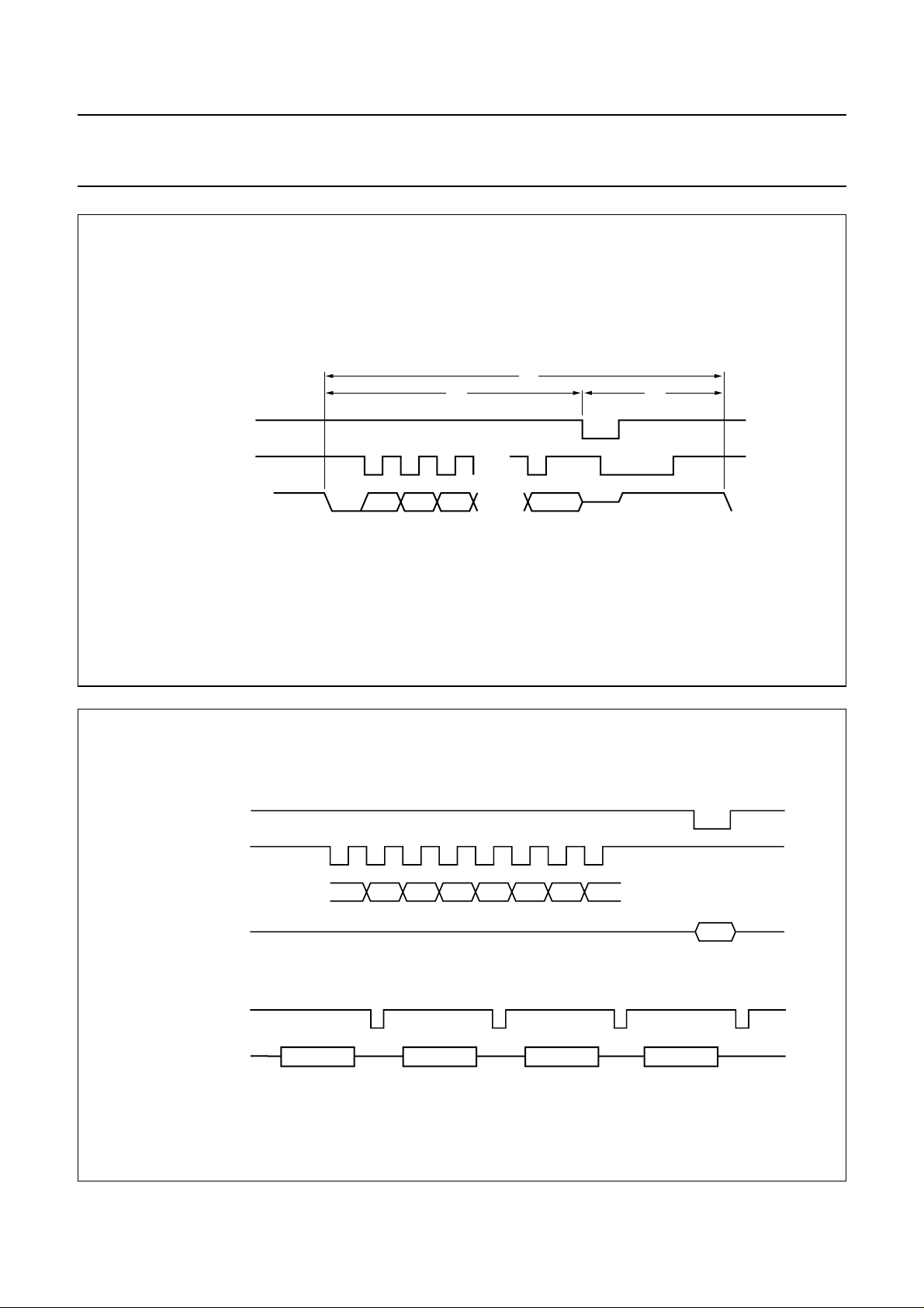
Philips Semiconductors Preliminary specification
Digital servo processor and Compact Disc
decoder (CD7)
t
1
RAB
(microcontroller)
SCL
(microcontroller)
SDA
(SAA7370A)
Q1 Q2 Q3 Qn
SAA7370A
t
2
t
3
MBG773
handbook, full pagewidth
(microcontroller)
(microcontroller)
(microcontroller)
(SAA7370A)
(microcontroller)
(microcontroller)
SILD
SCL
SDA
SDA
SILD
SDA
Fig.27 SUBQREADY-I status timing when subcode is read.
D7 D6 D5 D4 D3 D2 D1 D0
command or data byte
high-impedance
microcontroller write (one byte: command or data)
COMMAND DATA1 DATA2 DATA3
MBG776
microcontroller write (full command)
Fig.28 Microcontroller protocol for write servo commands.
1995 Nov 29 34
Page 35
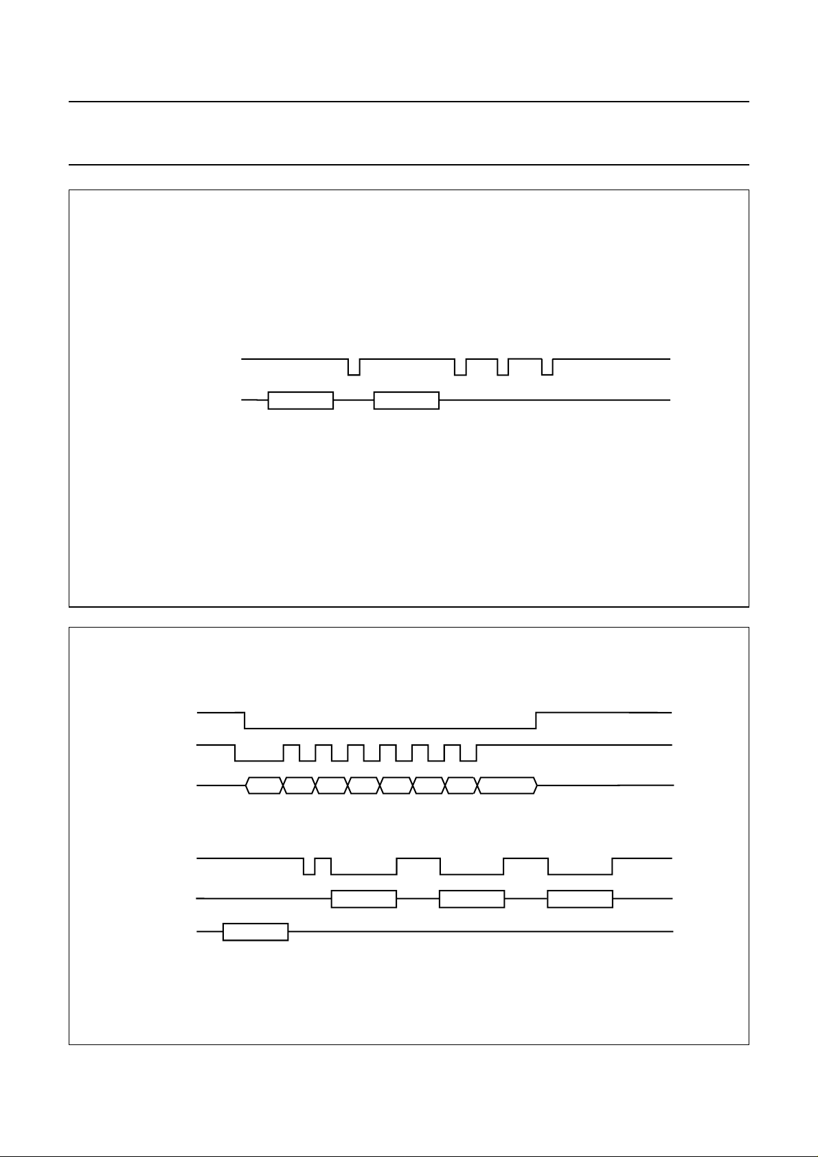
Philips Semiconductors Preliminary specification
Digital servo processor and Compact Disc
decoder (CD7)
handbook, full pagewidth
SILD
(microcontroller)
SDA
(microcontroller)
COMMAND DATA1
microcontroller write (full command)
SAA7370A
MBG413
handbook, full pagewidth
SILD
(microcontroller)
SCL
(microcontroller)
SDA (SAA7370A)
SILD
(microcontroller)
SDA (SAA7370A)
SDA
(microcontroller)
Fig.29 Microcontroller protocol for repeated data in write servo commands.
D7 D6 D5
COMMAND
D4 D3 D2
data byte
microcontroller read (one data byte)
DATA1 DATA2 DATA3
microcontroller read (full command)
D1 D0
MBG775
Fig.30 Microcontroller protocol for read servo commands.
1995 Nov 29 35
Page 36

Philips Semiconductors Preliminary specification
Digital servo processor and Compact Disc
SAA7370A
decoder (CD7)
7.15.3 SUMMARY OF FUNCTIONS CONTROLLED BY REGISTERS 0 TO F
Table 12 Registers 0 to F
REGISTER ADDRESS DATE FUNCTION INITIAL
0
(fade and
attenuation)
1
(motor mode)
2
(status control)
3
(DAC output)
0000 0000 mute reset
0010 attenuate −
0001 full scale −
0100 step down −
0101 step up −
0001 x000 motor off mode reset
x 001 motor stop mode 1 −
x010 motor stop mode 2 −
x011 motor start mode 1 −
x100 motor start mode 2 −
x101 motor jump mode −
x111 motor play mode −
x110 motor jump mode 1 −
1xxx anti-windup active −
0xxx anti-windup off reset
0010 0000 status = SUBQREADY-I reset
0001 status = MOTSTART1 −
0010 status = MOTSTART2 −
0011 status = MOTSTOP −
0100 status = PLL Lock −
0101 status = V1 −
0110 status = V2 −
0111 status = MOTOR-OV −
1000 status = FIFO overflow −
1001 status = shock detect −
1010 status = latched shock detect −
1011 status = latched shock detect reset −
0011 1010 I
2
S-bus; CD-ROM mode −
1011 EIAJ; CD-ROM mode −
1100 I
1111 I
1110 I
0000 EIAJ; 16-bit; 4f
0011 EAIJ; 16-bit; 2f
0010 EIAJ; 16-bit; f
0100 EIAJ; 18-bit; 4f
0111 EIAJ; 18-bit; 2f
0110 EIAJ; 18-bit; f
2
S-bus; 18-bit; 4fs mode reset
2
S-bus; 18-bit; 2fs mode −
2
S-bus; 16-bit; fs mode −
s
s
s
s
s
s
(1)
−
−
−
−
−
−
1995 Nov 29 36
Page 37
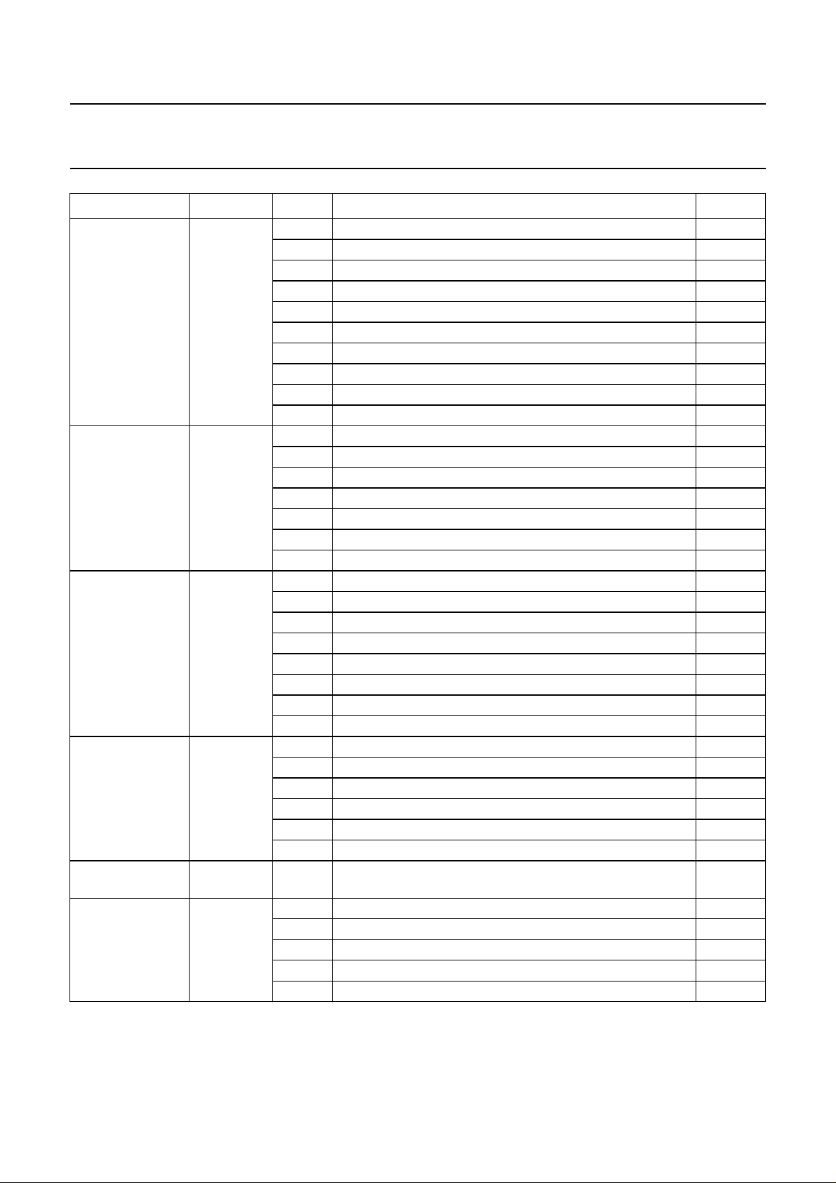
Philips Semiconductors Preliminary specification
Digital servo processor and Compact Disc
SAA7370A
decoder (CD7)
REGISTER ADDRESS DATE FUNCTION INITIAL
4
(motor gain)
5
(motor bandwidth)
6
(motor output
configuration)
7
(DAC output and
status control)
8 (PLL loop filter
bandwidth)
9
(PLL equalization)
0100 x000 motor gain G = 3.2 reset
x001 motor gain G = 4.0 −
x010 motor gain G = 6.4 −
x011 motor gain G = 8.0 −
x100 motor gain G = 12.8 −
x101 motor gain G = 16.0 −
x110 motor gain G = 25.6 −
x111 motor gain G = 32.0 −
0xxx disable comparator clock divider reset
1xxx enable comparator clock divider; only if SELLPLL set HIGH −
0101 xx00 motor f4 = 0.5 × n Hz reset
xx01 motor f4 = 0.7 × nHz −
xx10 motor f4 = 1.4 × nHz −
xx11 motor f4 = 2.8 × nHz −
00xx motor f3 = 0.85 × n Hz reset
01xx motor f3 = 1.71 × nHz −
10xx motor f3 = 3.42 × nHz −
0110 xx00 motor power maximum 37% reset
xx01 motor power maximum 50% −
xx10 motor power maximum 75% −
xx11 motor power maximum 100% −
00xx MOTO1, MOTO2 pins 3-state reset
01xx motor PWM mode −
10xx motor PDM mode −
11xx motor CDV mode −
0111 xx00 interrupt signal from servo at STATUS pin reset
xx10 status bit from decoder status register at STATUS pin −
x0xx DAC data normal value reset
x1xx DAC data inverted value −
0xxx left channel first at DAC (WCLK normal) reset
1xxx right channel first at DAC (WCLK inverted) −
see Table 13 −
1001 0011 PLL loop filter equalization reset
0001 PLL 30 ns over-equalization −
0010 PLL 15 ns over-equalization −
0100 PLL 15 ns under-equalization −
0101 PLL 30 ns under-equalization −
(1)
1995 Nov 29 37
Page 38
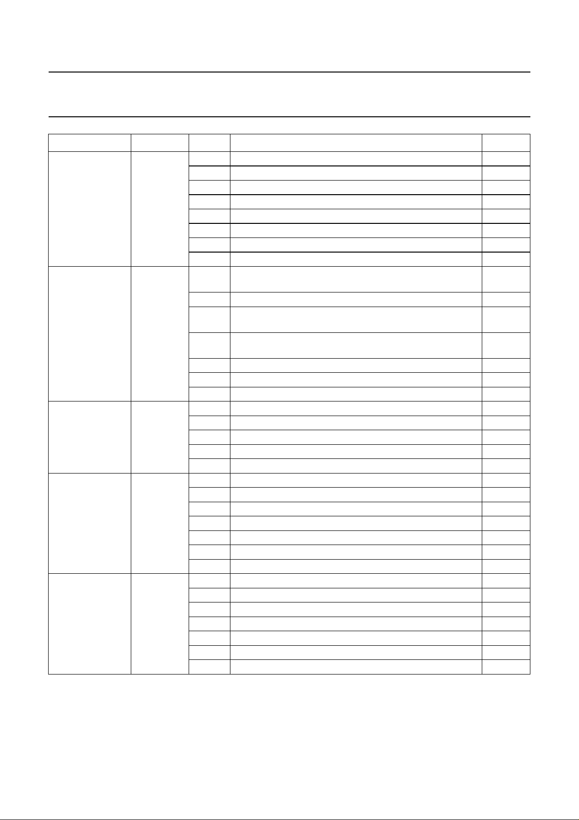
Philips Semiconductors Preliminary specification
Digital servo processor and Compact Disc
SAA7370A
decoder (CD7)
REGISTER ADDRESS DATE FUNCTION INITIAL
A
(EBU output)
B
(speed control)
C
(versatile pins
interface)
D
(versatile pins
interface)
E 1110 0xxx bit controls operating speed mode, see register B reset
1010 xx0x EBU data before concealment −
xx1x EBU data after concealment and fade reset
x0x0 level II clock accuracy (<1000 ppm) reset
x0x1 level I clock accuracy (<50 ppm) −
x1x0 level III clock accuracy (>1000 ppm) −
x1x1 EBU off - output low −
0xxx flags in EBU off reset
1xxx flags in EBU on −
1011 x0xx 33.8688 MHz crystal present, or 8.4672 MHz (or
16.9344 MHz) crystal with SELPLL set HIGH
x1xx 16.9344 MHz crystal present (single-speed mode only) −
0xxx single-speed mode (if register E = 0xxx) four times speed
mode (if register E = 1xxx); note 2
1xxx double-speed mode (if register E = 0xxx) eight times speed
mode (if register E = 1xxx); note 2
xx00 standby 1: ‘CD-STOP’ mode reset
xx10 standby 2: ‘CD-PAUSE’ mode −
xx11 operating mode −
1100 xxx1 external off-track signal input at V1 −
xxx0 internal off-track signal used (V1 may be read via status) reset
xx0x kill-L at KILL output, kill-R at V3 output −
001x V3 = 0; single KILL output reset
011x V3 = 1; single KILL output −
1101 0000 4-line motor (using V4 and V5) −
xx01 Q-to-W subcode at V4 −
xx10 V4 = 0 −
xx11 V4 = 1 reset
01xx de-emphasis signal at V5, no internal de-emphasis filter −
10xx V5 = 0 −
11xx V5 = 1 reset
x0xx audio features disabled −
x1xx audio features enabled reset
xx0x lock-to-disc mode disabled reset
xx1x lock-to-disc mode enabled −
xxx0 motor brakes to 12% reset
xxx1 motor brakes to 6% −
reset
reset
−
(1)
1995 Nov 29 38
Page 39
Philips Semiconductors Preliminary specification
Digital servo processor and Compact Disc
SAA7370A
decoder (CD7)
REGISTER ADDRESS DATE FUNCTION INITIAL
F
(subcode
interface)
Note
1. The initial column shows the power-on reset state.
2. The speed is doubled if using a 16.9344 MHz crystal with SELPLL set HIGH.
Table 13 Loop filter bandwidth
REGISTER ADDRESS DATA
8
(PLL loop filter
bandwidth)
1111 x000 subcode interface off reset
x100 subcode interface on −
0xxx 4-wire subcode reset
1xxx 3-wire subcode −
FUNCTION
INTERNAL
BANDWIDTH
(Hz)
1000 0000 1640 × n 525 × n 8400 × n −
0001 3279 × n 263 × n 16800 × n −
0010 6560 × n 131 × n 33600 × n −
0100 1640 × n 1050 × n 8400 × n −
0101 3279 × n 525 × n 16800 × n −
0110 6560 × n 263 × n 33600 × n −
1000 1640 × n 2101 × n 8400 × n −
1001 3279 × n 1050 × n 16800 × n reset
1010 6560 × n 525 × n 33600 × n −
1100 1640 × n 4200 × n 8400 × n −
1101 3279 × n 2101 × n 16800 × n −
1110 6560 × n 1050 × n 33600 × n −
BANDWIDTH
(Hz)
LOW-PASS
BANDWIDTH
(Hz)
INITIAL
(1)
(1)LOOP
Note
1. The initial column shows the power-on reset state.
1995 Nov 29 39
Page 40
Philips Semiconductors Preliminary specification
Digital servo processor and Compact Disc
SAA7370A
decoder (CD7)
7.15.4 SUMMARY OF SERVO COMMANDS
A list of the servo commands are given in Table 14. It should be noted that these are not fully backwards compatible with
DSIC2.
Table 14 CD7 servo commands
COMMANDS CODE BYTES PARAMETERS
Write commands
Write_focus_coefs1 17H 7 <foc_parm3> <foc_int> <ramp_incr> <ramp_height> <ramp_offset>
<FE_start> <foc_gain>
Write_focus_coefs2 27H 7 <defect_parm> <rad_parm_jump> <vel_parm2> <vel_parm1>
<foc_parm1> <foc_parm2> <CA_drop>
Write_focus_command 33H 3 <foc_mask> <foc_stat> <shock_level>
Focus_gain_up 42H 2 <foc_gain> <foc_parm1>
Focus_gain_down 62H 2 <foc_gain> <foc_parm1>
Write_radial coefs 57H 7 <rad_length_lead> <rad_int> <rad_parm_play> <rad_pole_noise>
<rad_gain> <sledge_parm2> <sledge_parm_1>
Preset_Latch 81H 1 <chip_init>
Radial_off C1H 1 ‘1CH’
Radial_init C1H 1 ‘3CH’
Short_jump C3H 3 <tracks_hi> <tracks_lo> <rad_stat>
Long_jump C5H 5 <brake_dist> <sledge_U_max> <tracks_hi> <tracks_lo> <rad_stat>
Steer_sledge B1H 1 <sledge_level>
Preset_init 93H 3 <re_offset> <re_gain> <sum_gain>
Write_decoder_reg
Write_parameter A2H 2 <param_ram_addr> <param_data>
(1)
D1H 1 <decoder_reg_data>
Read commands
Read_Q_subcode
Read_status 70H up to 5 <foc_stat> <rad_stat> <rad_int_lpf> <tracks_hi> <tracks_lo>
Read_hilevel_status
Read_aux_status F0H up to 3 <re_offset> <re_gain> <sum_gain>
Notes
1. These commands only available when internal decoder interface is enabled.
2. <peak_l> and <peak_r> bytes are clocked out LSB first.
3. Decoder status flag information in <dec_stat> is only valid when the internal decoder interface is enabled.
1995 Nov 29 40
(1)(2)
0H up to 12 <Q_sub1..10> <peak_l> <peak_r>
(3)
E0H up to 4 <intreq> <dec_stat> <seq_stat> <motor_start_time>
Page 41
Philips Semiconductors Preliminary specification
Digital servo processor and Compact Disc
SAA7370A
decoder (CD7)
7.15.5 SUMMARY OF SERVO COMMAND PARAMETERS
Table 15 Servo command parameters
PARAMETER
foc_parm_1 − focus PID − end of focus lead
foc_parm_2 − focus PID − focus low-pass
foc_parm_3 − focus PID − focus lead length
foc_int 14H focus PID − focus integrator crossover frequency
foc_gain 15H focus PID 70H focus PID loop gain
CA_drop 12H focus PID − sensitivity of drop-out detector
ramp_offset 16H focus ramp − asymmetry of focus ramp
ramp_height 18H focus ramp − peak-to-peak value of ramp voltage
ramp_incr − focus ramp − slope of ramp voltage
FE_start 19H focus ramp − minimum value of focus error
rad_parm_play 28H radial PID − end of radial lead
rad_pole_noise 29H radial PID − radial low-pass
rad_length_lead 1CH radial PID − length of radial lead
rad_int 1EH radial PID − radial integrator crossover frequency
rad_gain 2AH radial PID 70H radial loop gain
rad_parm_jump 27H radial jump − filter during jump
vel_parm1 1FH radial jump − PI controller crossover frequencies
vel_parm2 32H radial jump − jump pre-defined profile
speed_threshold 48H radial jump − maximum speed in fastrad mode
hold_mult 49H radial jump 00H electronic damping
brake_dist_max 21H radial jump − maximum sledge distance allowed in fast actuator
sledge_long_brake 58H radial jump 7FH brake distance of sledge
sledge_Umax − sledge − voltage on sledge during long jump
sledge_level − sledge − voltage on sledge when steered
sledge_parm_1 36H sledge − sledge integrator crossover frequency
sledge_parm_2 17H sledge − sledge low-pass frequencies
sledge_pulse1 46H pulsed sledge − pulse width
sledge_pulse2 64H pulsed sledge − pulse height
defect_parm − defect detector − defect detector setting
shock_level − shock detector − shock detector operation
playwatchtime 54H watchdog − radial on-track watchdog time
RAM
ADDRESS
AFFECTS
POR
VALUE
DETERMINES
defect detector enabling
focus error normalising
minimum light level
sledge bandwidth during jump
steered mode
sledge gain
sledge operation mode
1995 Nov 29 41
Page 42

Philips Semiconductors Preliminary specification
Digital servo processor and Compact Disc
SAA7370A
decoder (CD7)
PARAMETER
jumpwatchtime 57H watchdog − radial jump watchdog time-out
radcontrol 59H watchdog − enable/disable automatic radial off feature
chip_init − set-up − V
xtra_preset 4AH set-up 38H laser on/off
cd6cmd 4DH decoder interface − decoder part commands
interrupt_mask 53H STATUS pin − enabled interrupts
seq_control 42H autosequencer − autosequencer control
focus_start_time 5EH autosequencer − focus start time
motor_start_time1 5FH autosequencer − motor start 1 time
motor_start_time2 60H autosequencer − motor start 2 time
radial_init_time 61H autosequencer − radial initialization time
brake_time 62H autosequencer − brake time
RadCmdByte 63H autosequencer − radial command byte
osc_inc 68H focus/radial AGC − AGC control
phase_shift 67H focus/radial AGC − phase shift of injected signal
level1 69H focus/radial AGC − amplitude of signal injected
level2 6AH focus/radial AGC − amplitude of signal injected
agc_gain 6CH focus/radial AGC − focus/radial gain
RAM
ADDRESS
AFFECTS
POR
VALUE
DETERMINES
level setting
RH
enable/disable decoder interface
RA, FO and SL PDM modulating frequency
microcontroller communication to decoder part
fast jumping circuit on/off
frequency of injected signal
1995 Nov 29 42
Page 43
Philips Semiconductors Preliminary specification
Digital servo processor and Compact Disc
SAA7370A
decoder (CD7)
8 LIMITING VALUES
In accordance with the Absolute Maximum Rating System (IEC 134).
SYMBOL PARAMETER CONDITIONS MIN. MAX. UNIT
V
DD
V
I(max)
V
O
V
DDdiff
I
O
I
IK
V
es
T
amb
T
stg
Notes
1. All V
and VSS connections must be made externally to the same power supply.
DD
2. Equivalent to discharging a 100 pF capacitor via a 1.5 kΩ series resistor with a rise time of 15 ns.
3. Equivalent to discharging a 200 pF capacitor via a 2.5 µH series inductor.
supply voltage note 1 −0.5 +6.5 V
maximum Input voltage (any input) −0.5 VDD+ 0.5 V
output voltage (any output) −0.5 +6.5 V
difference between V
DDA
and V
DDD
−± 0.25 V
output current (continuous) −± 20 mA
DC input diode current (continuous) −± 20 mA
electrostatic handling note 2 −2000 +2000 V
note 3 −200 +200 V
operating ambient temperature 0 +70 °C
storage temperature −55 +125 °C
9 CHARACTERISTICS
= 4.75 to 5.25 V; VSS=0V; T
V
DD
= 0 to +70 °C; unless otherwise specified.
amb
SYMBOL PARAMETER CONDITIONS MIN. TYP. MAX. UNIT
Supply
V
DD
I
DD
supply voltage 4.75 5.0 5.25 V
supply current VDD=5V;
− 49 − mA
n = 1 mode
Decoder analog front-end (V
C
OMPARATOR INPUTS: HFIN AND HFREF
f
clk
V
th(sw)
V
15
REFERENCE GENERATOR:I
V
Iref
clock frequency note 1 8 − 140 MHz
switching voltage threshold 1.2 − VDD− 0.8 V
input voltage level (pin 15) − 1.0 − V
REF
reference voltage level
DDA
=5V; V
SSA
=0V; T
amb
=25°C)
− 0.5V
DD
− V
(pin 18)
1995 Nov 29 43
Page 44
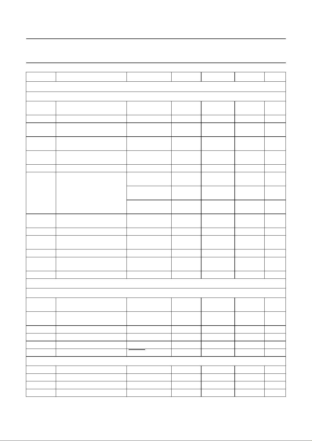
Philips Semiconductors Preliminary specification
Digital servo processor and Compact Disc
SAA7370A
decoder (CD7)
SYMBOL PARAMETER CONDITIONS MIN. TYP. MAX. UNIT
Servo analog part (V
P
INS D1 TO D4, R1, R2, V
I
refT
input reference current
(pin 10)
R
V
IrefT
IrefT
external resistor on pin 10 220 − 620 kΩ
voltage on reference current
input (pin 10)
I
D(max)
maximum input current for
central diode input signal
I
R(max)
maximum input current for
satellite diode input signal
V
RL
V
RH
LOW level reference voltage 0 0 0 V
HIGH level reference voltage output state 0;
(THD+N)/S total harmonic distortion plus
noise
S/N signal-to-noise ratio − 55 − dB
PSRR power supply rejection at
V
DDA2
G
tol
G
v
gain tolerance note 6 −12 0 +12 %
variation of gain between
channels
α
cs
channel separation − 60 − dΒ
Digital inputs
DDA
=5V; V
RH,VRL
SSA
AND I
=0V; T
refT
=25°C)
amb
1.935 − 5.45 µA
− 1.2 − V
note 2 3.871 − 10.9 µA
note 2 1.935 − 5.45 µA
− 0.5 − V
note 3
output state v;
−30% 0.5 × 10
v/44.4
+30% V
note 3
output state 31;
− 2.5 − V
note 3
at 0 dB; note 4 −−50 −45 dB
note 5 − 45 − dB
−− 2%
NPUTS: RESET, V1, V2, SELPLL (CMOS INPUT WITH PULL-UP RESISTOR AND HYSTERESIS)
I
V
thr(sw)
switching voltage threshold
−− 0.8V
rising
V
thf(sw)
switching voltage threshold
0.2V
DDD
−−V
falling
V
hys
R
I(pu)
C
in
t
resL
hysteresis voltage − 0.33V
input pull-up resistance Vi=0V − 50 − kΩ
input capacitance −− 10 pF
reset pulse width (active LOW) RESET only 1 −−µs
INPUTS: SCL, RAB, SILD AND RCK (CMOS INPUT)
V
IL
V
IH
I
LI
C
in
LOW level input voltage −0.3 − 0.3V
HIGH level input voltage 0.7V
input leakage current Vi=0−V
DDD
−10 − +10 µA
DDD
− V
input capacitance −− 10 pF
1995 Nov 29 44
DDD
DDD
− V
DDD
+ 0.3 V
DDD
V
V
Page 45
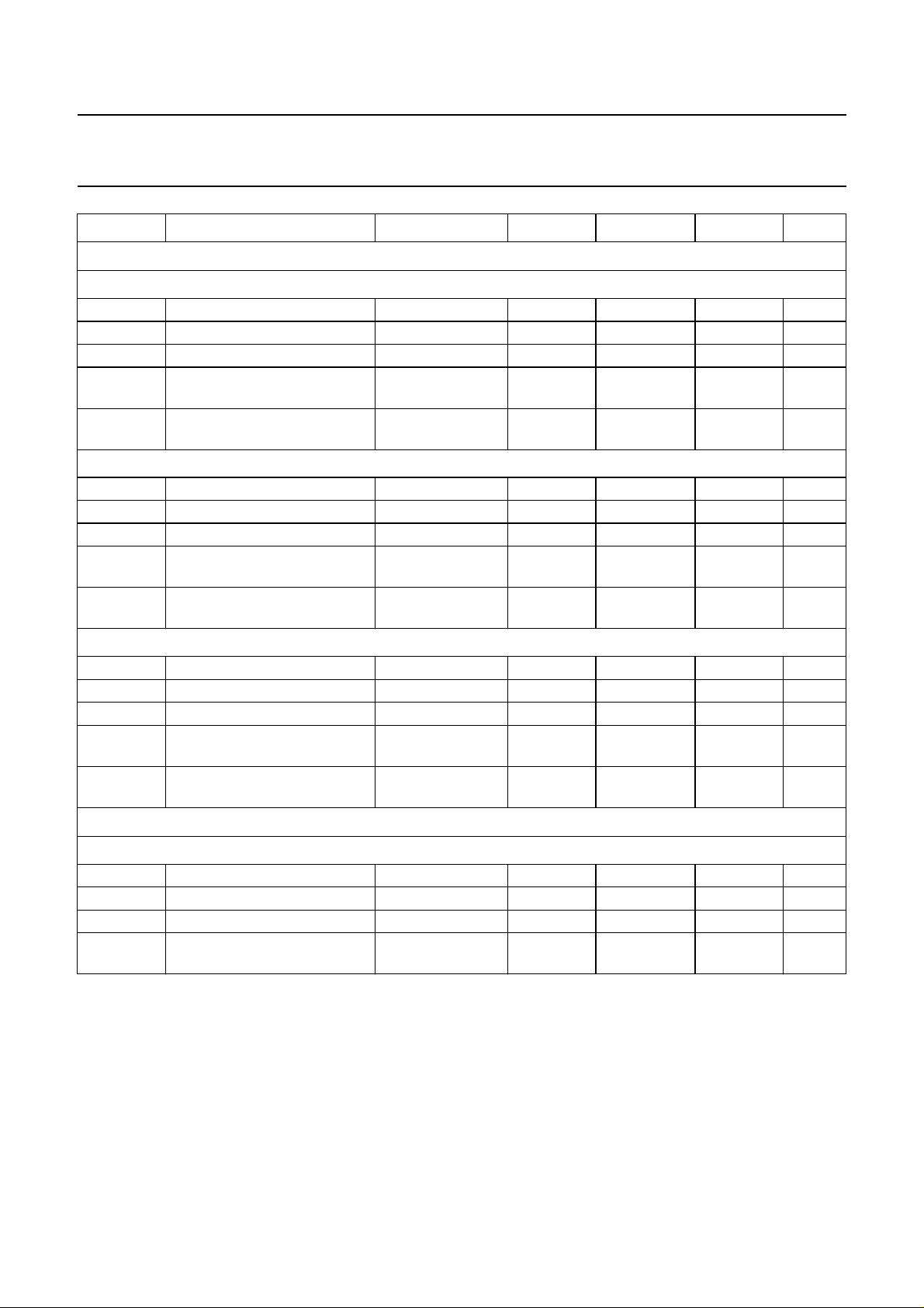
Philips Semiconductors Preliminary specification
Digital servo processor and Compact Disc
SAA7370A
decoder (CD7)
SYMBOL PARAMETER CONDITIONS MIN. TYP. MAX. UNIT
Digital outputs
OUTPUT: CL4
V
OL
V
OH
C
L
t
r
t
f
OUTPUT: CL16
V
OL
V
OH
C
L
t
r
t
f
OUTPUTS:V4AND V5
V
OL
V
OH
C
L
t
r
t
f
Open-drain outputs
LOW level output voltage IOL= 1 mA 0 − 0.4 V
HIGH level output voltage IOH= −1mA V
− 0.4 − V
DDD
DDD
V
load capacitance −− 25 pF
output rise time CL= 20 pF;
0.8 to (V
DDD
output fall time CL= 20 pF;
(V
− 0.8) to 0.8
DDD
− 0.8)
−− 20 ns
−− 20 ns
LOW level output voltage IOL= 1 mA 0 − 0.4 V
HIGH level output voltage IOH= −1mA V
− 0.4 − V
DDD
DDD
V
load capacitance −− 50 pF
output rise time CL= 20 pF;
0.8 − (V
DDD
output fall time CL= 20 pF;
(V
− 0.8) − 0.8
DDD
− 0.8)
−− 15 ns
−− 15 ns
LOW level output voltage IOL=10mA 0 − 1.0 V
HIGH level output voltage IOH= −10 mA V
− 1 − V
DDD
DDD
V
load capacitance −− 50 pF
output rise time CL= 20 pF;
0.8 − (V
DDD
output fall time CL= 20 pF;
(V
− 0.8) − 0.8
DDD
− 0.8)
−− 10 ns
−− 10 ns
O
UTPUTS: CFLG, C2FAIL, STATUS, KILL, V3 AND LDON (OPEN-DRAIN OUTPUT WITH PROTECTION DIODE TO V
V
OL
I
OL
C
L
t
f
LOW level output voltage IOL= 1 mA 0 − 0.4 V
LOW level output current −− 2mA
load capacitance −− 25 pF
output fall time CL= 20 pF;
(V
− 0.8) − 0.8
DDD
−− 30 ns
1995 Nov 29 45
DD
)
Page 46
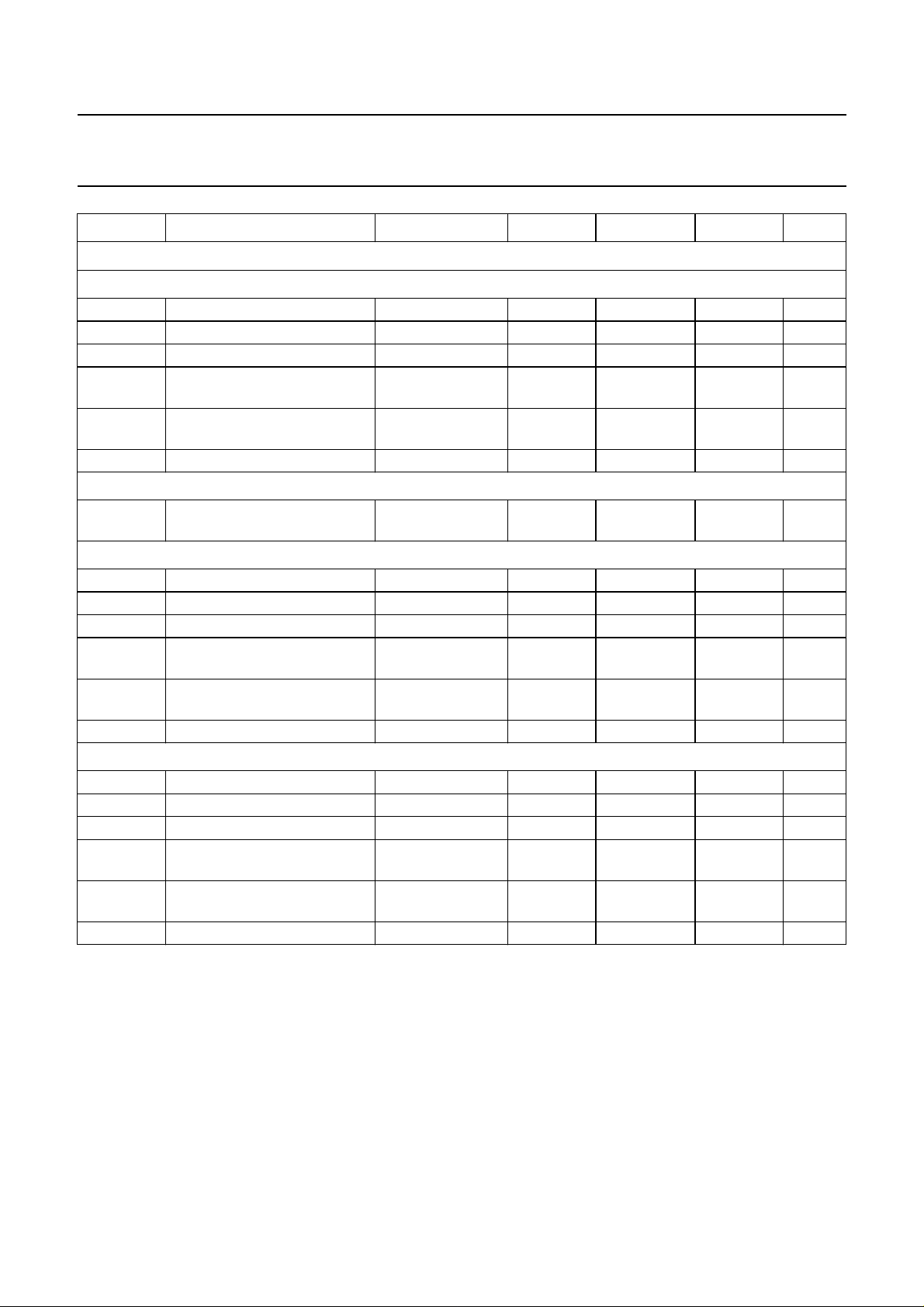
Philips Semiconductors Preliminary specification
Digital servo processor and Compact Disc
SAA7370A
decoder (CD7)
SYMBOL PARAMETER CONDITIONS MIN. TYP. MAX. UNIT
3-state outputs
OUTPUTS: EF, CLK, WCLK, DATA AND CL11
V
OL
V
OH
C
L
t
r
t
f
I
ZO
OUTPUT: CL11
t
H
OUTPUTS: RA, FO, SL, SBSY, SFSY AND SUB
V
OL
V
OH
C
L
t
r
t
f
I
ZO
OUTPUTS: MOTO1, MOTO2 AND DOBM
V
OL
V
OH
C
L
t
r
t
f
I
ZO
LOW level output voltage IOL= 1 mA 0 − 0.4 V
HIGH level output voltage IOH= −1mA VDD− 0.4 − V
DD
V
load capacitance −− 50 pF
output rise time CL= 20 pF;
−− 15 ns
0.8 − (VDD− 0.8)
output fall time CL= 20 pF;
−− 15 ns
(VDD− 0.8) − 0.8
output 3-state leakage current Vi=0−V
output HIGH time (relative to
Vo=1.5V4550 55%
DD
−10 − +10 µA
clock period)
LOW level output voltage IOL= 1 mA 0 − 0.4 V
HIGH level output voltage IOH= −1mA VDD− 0.4 − V
DD
V
load capacitance −− 25 pF
output rise time CL= 20 pF;
−− 20 ns
0.8 − (VDD− 0.8)
output fall time CL= 20 pF;
−− 20 ns
(VDD− 0.8) − 0.8
3-state leakage current Vi=0−V
DD
−10 − +10 µA
LOW level output voltage IOL=10mA 0 − 1.0 V
HIGH level output voltage IOH= −10 mA VDD− 1 − V
DD
V
load capacitance −− 50 pF
output rise time CL= 20 pF;
−− 10 ns
0.8 − (VDD− 0.8)
output fall time CL= 20 pF;
−− 10 ns
(VDD− 0.8) − 0.8
3-state leakage current Vi=0−V
DD
−10 − +10 µA
1995 Nov 29 46
Page 47
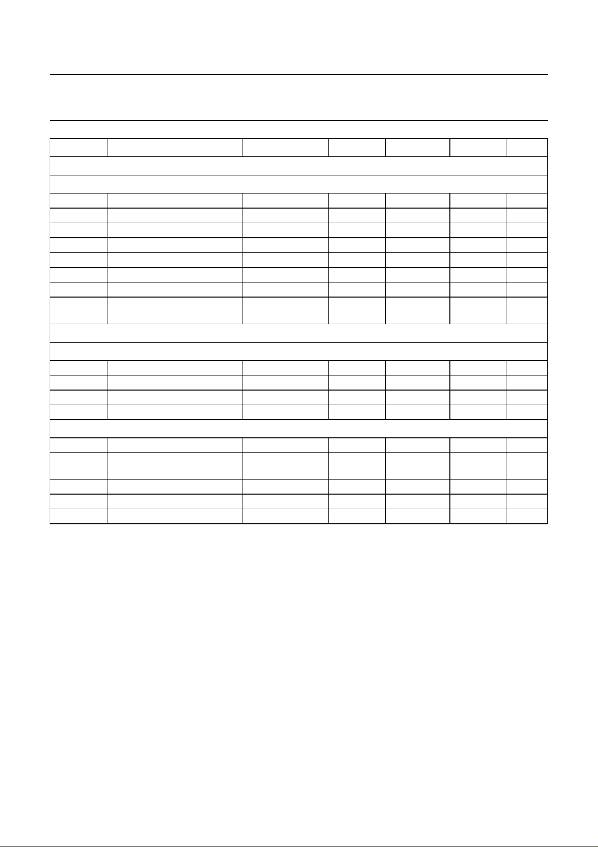
Philips Semiconductors Preliminary specification
Digital servo processor and Compact Disc
SAA7370A
decoder (CD7)
SYMBOL PARAMETER CONDITIONS MIN. TYP. MAX. UNIT
Digital input/output
INPUT/OUTPUT: SDA [CMOS INPUT/OPEN-DRAIN I2C-BUS OUTPUT (WITH PROTECTION DIODE TO V
V
IL
V
IH
I
ZO
C
in
V
OL
I
OL
C
L
t
f
LOW level input voltage −0.3 − 0.3V
HIGH level input voltage 0.7V
3-state leakage current Vi=0−V
DDD
−10 − +10 µA
DDD
− V
input capacitance −− 10 pF
LOW level output voltage IOL= 2 mA 0 − 0.4 V
LOW level output current −− 4mA
load capacitance −− 50 pF
output fall time CL= 20 pF;
(V
− 0.8) − 0.8
DDD
−− 15 ns
Crystal oscillator
I
NPUT: CRIN (EXTERNAL CLOCK)
V
IL
V
IH
I
LI
C
in
LOW level input voltage −0.3 − 0.3V
HIGH level input voltage 0.7V
DD
− VDD+ 0.3 V
input leakage current −10 − +10 µA
input capacitance −− 10 pF
OUTPUT: CROUT; see Figs 3 and 4
f
g
xtal
m
crystal frequency note 7 8 8.4672 35 MHz
mutual conductance at
− 10 − mA/V
100 kHz
G
v
C
fb
C
out
small signal voltage gain Gv=gm×R
O
− 18 − V/V
feedback capacitance −− 5pF
output capacitance −− 10 pF
Notes
1. Highest clock frequency at which data slicer produces 1010 output in analog self-test mode.
2. VRL= 0 V, f
to I
refT:
a) For D1 to D4: I
b) For R1 and R2:I
= 4.2336 MHz. The maximum input current depends on the value of the external resistor connected
sys
max
max
= 2.4/R
= 1.2/R
⇒ 2.4/220 kΩ = 10.9 µA.
IrefT
⇒ 1.2/220 kΩ = 5.45 µA.
IrefT
3. Internal reference source with 32 different output voltages. Selection is achieved during a calibration period or via
the serial interface. The values given are for an unloaded VRH.
4. VRH= 2.5 V and VRL= 0 V, measuring bandwidth: 200 Hz to 20 kHz, f
5. f
6. Gain of the ADC is defined as G
ripple
= 1 kHz, V
= 0.5 V (p-p).
ripple
ADC=fsys/Imax
(counts/µA); thus digital output = Ii× G
i(ADC)
= 1 kHz.
ADC
a) Digital output = the number of pulses at the digital output in counts/s and Ii= the DC input current in µA.
b) The maximum input current depends on the system frequency (f
= 4.2336 MHz) and on VRH− VRL.
sys
c) The gain tolerance is the deviation from the calculated gain regarding note 2.
7. It is recommended that the series resistance of the crystal or ceramic resonator is ≤60 Ω.
)]
DDD
DDD
where:
DDD
+ 0.3 V
DD
V
V
1995 Nov 29 47
Page 48
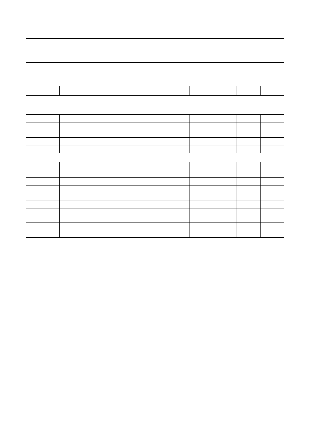
Philips Semiconductors Preliminary specification
Digital servo processor and Compact Disc
SAA7370A
decoder (CD7)
10 OPERATING CHARACTERISTICS (SUBCODE INTERFACE TIMING)
= 4.75 to 5.25 V; VSS=0V; T
V
DD
SYMBOL PARAMETER CONDITIONS MIN. TYP. MAX. UNIT
Subcode interface timing (single speed × n); see Fig.31; note 1
I
NPUT: RCK
t
H
t
L
t
r
t
f
t
dC
input clock HIGH time 2/n 4/n 6/n µs
input clock LOW time 2/n 4/n 6/n µs
input clock rise time −−80/n ns
input clock fall time −−80/n ns
delay time SFSY to RCK 10/n − 20/n µs
OUTPUTS: SBSY, SFSY AND SUB (CL=20pF)
t
Bcy
t
BW
t
Fcy
t
FW
t
FH
t
FL
t
dPAC
block cycle 12.0/n 13.3/n 14.7/n ms
SBSY pulse width −−300/n µs
frame cycle 122/n 136/n 150/n µs
SFSY pulse width (3-wire mode only) −−366/n µs
SFSY HIGH time −−66/n µs
SFSY LOW time −−84/n µs
delay time SFSY to SUB (P data)
valid
t
dAC
t
hD
delay time RCK falling to SUB −−0µs
hold time RCK to SUB −−0.7/n µs
= 0 to +70 °C; unless otherwise specified.
amb
−−1/n µs
Note
1. The subcode timing is directly related to the overspeed factor ‘n’ in normal operating mode. ‘n’ is replaced by the disc
speed factor ‘d’, in the lock-to-disc mode.
1995 Nov 29 48
Page 49
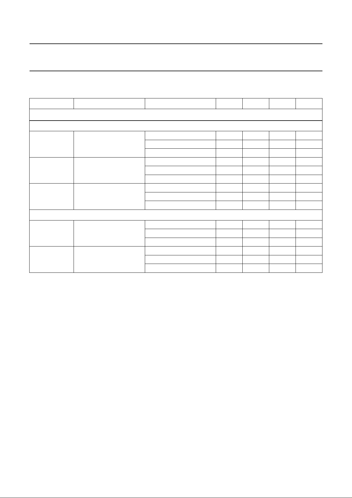
Philips Semiconductors Preliminary specification
Digital servo processor and Compact Disc
SAA7370A
decoder (CD7)
11 OPERATING CHARACTERISTICS (I2S-BUS TIMING)
= 4.75 to 5.25 V; VSS=0V; T
V
DD
SYMBOL PARAMETER CONDITIONS MIN. TYP. MAX. UNIT
2
I
S-bus timing (single speed × n); see Fig.32; note 1
CLOCK OUTPUT: SCLK (CL=20pF)
T
t
t
cy
CH
CL
output clock period sample rate = f
clock HIGH time sample rate = f
clock LOW time sample rate = f
OUTPUTS: WCLK, DATA AND EF (CL= 20 pF)
t
su
t
h
set-up time sample rate = f
hold time sample rate = f
= 0 to +70 °C; unless otherwise specified
amb
s
sample rate = 2f
sample rate = 4f
sample rate = 2f
sample rate = 4f
sample rate = 2f
sample rate = 4f
sample rate = 2f
sample rate = 4f
sample rate = 2f
sample rate = 4f
s
s
s
s
s
s
s
s
s
s
s
s
s
s
− 472.4/n − ns
− 236.2/n − ns
− 118.1/n − ns
166/n −−ns
83/n −−ns
42/n −−ns
166/n −−ns
83/n −−ns
42/n −−ns
95/n −−ns
48/n −−ns
24/n −−ns
95/n −−ns
48/n −−ns
24/n −−ns
Note
1. The I
2
S-bus timing is directly related to the overspeed factor ‘n’ in the normal operating mode. In the lock-to-disc
mode ‘n’ is replaced by the disc speed factor ‘d’.
1995 Nov 29 49
Page 50
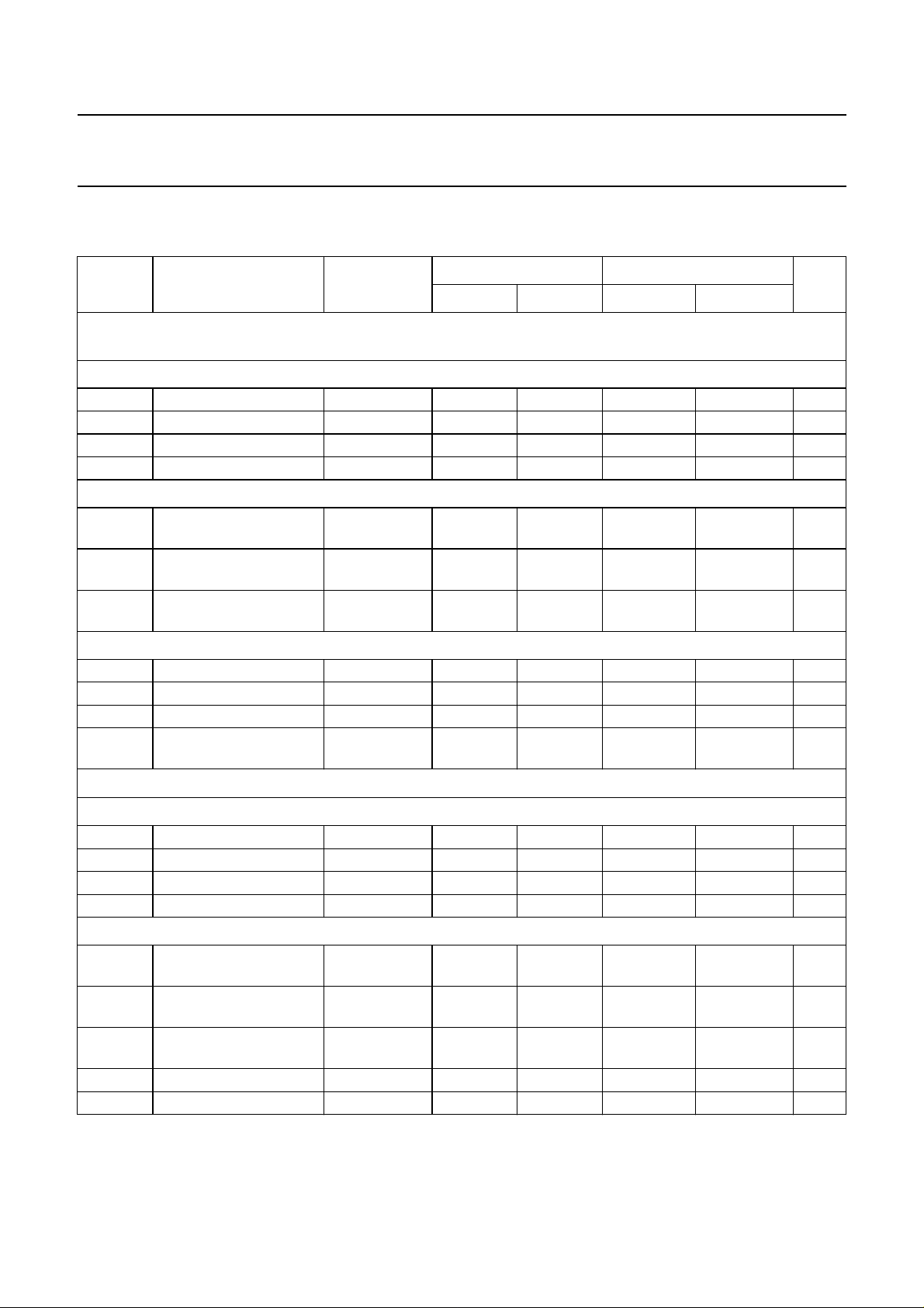
Philips Semiconductors Preliminary specification
Digital servo processor and Compact Disc
SAA7370A
decoder (CD7)
12 OPERATING CHARACTERISTICS (MICROCONTROLLER INTERFACE TIMING)
= 4.75 to 5.25 V; VSS=0V; T
V
DD
SYMBOL PARAMETER CONDITIONS
Microcontroller interface timing (4-wire bus mode; writing to registers 0 to F; reading Q-channel subcode and
decoder status); see Figs 33 and 34; note 1
I
NPUTS SCL AND RAB
t
CL
t
CH
t
r
t
f
input LOW time 480/n + 20 − 2400/n + 20 − ns
input HIGH time 480/n + 20 − 2400/n + 20 − ns
rise time − 480/n − 480/n ns
fall time − 480/n − 480/n ns
READ MODE (CL= 20 pF)
t
dRD
delay time RAB to SDA
valid
t
PD
propagation delay SCL
to SDA
t
dRZ
delay time RAB to SDA
high-impedance
WRITE MODE ((CL= 20 pF)
t
suD
t
hD
t
suCR
t
dWZ
set-up time SDA to SCL note 2 20 − 720/n − 20 − 720/n − ns
hold time SCL to SDA − 960/n + 20 − 4800/n + 20 ns
set-up time SCL to RAB 240/n + 20 − 1200/n + 20 − ns
delay time SDA
high-impedance to RAB
= 0 to +70 °C; unless otherwise specified.
amb
NORMAL MODE LOCK-TO-DISC MODE
MIN. MAX. MIN. MAX.
− 50 − 50 ns
720/n − 20 960/n + 20 720/n + 20 4800/n + 20 ns
− 50 − 50 ns
0 − 0 − ns
UNIT
Microcontroller interface timing (4-wire bus mode; servo commands); see Figs 35 and 36; notes 3 and 4
I
NPUTS SCL AND SILD
t
L
t
H
t
r
t
f
Input LOW time 710 − 710 − ns
Input HIGH time 710 − 710 − ns
rise time − 240 − 240 ns
fall time − 240 − 240 ns
READ MODE (CL= 20 pF)
t
dLD
delay time SILD to SDA
− 25 − 25 ns
valid
t
PD
propagation delay SCL
− 950 − 950 ns
to SDA
t
dLZ
delay time SILD to SDA
− 50 − 50 ns
high-impedance
t
sCLR
t
hCLR
set-up time SCL to SILD 480 − 480 − ns
hold time SILD to SCL 830 − 830 − ns
1995 Nov 29 50
Page 51
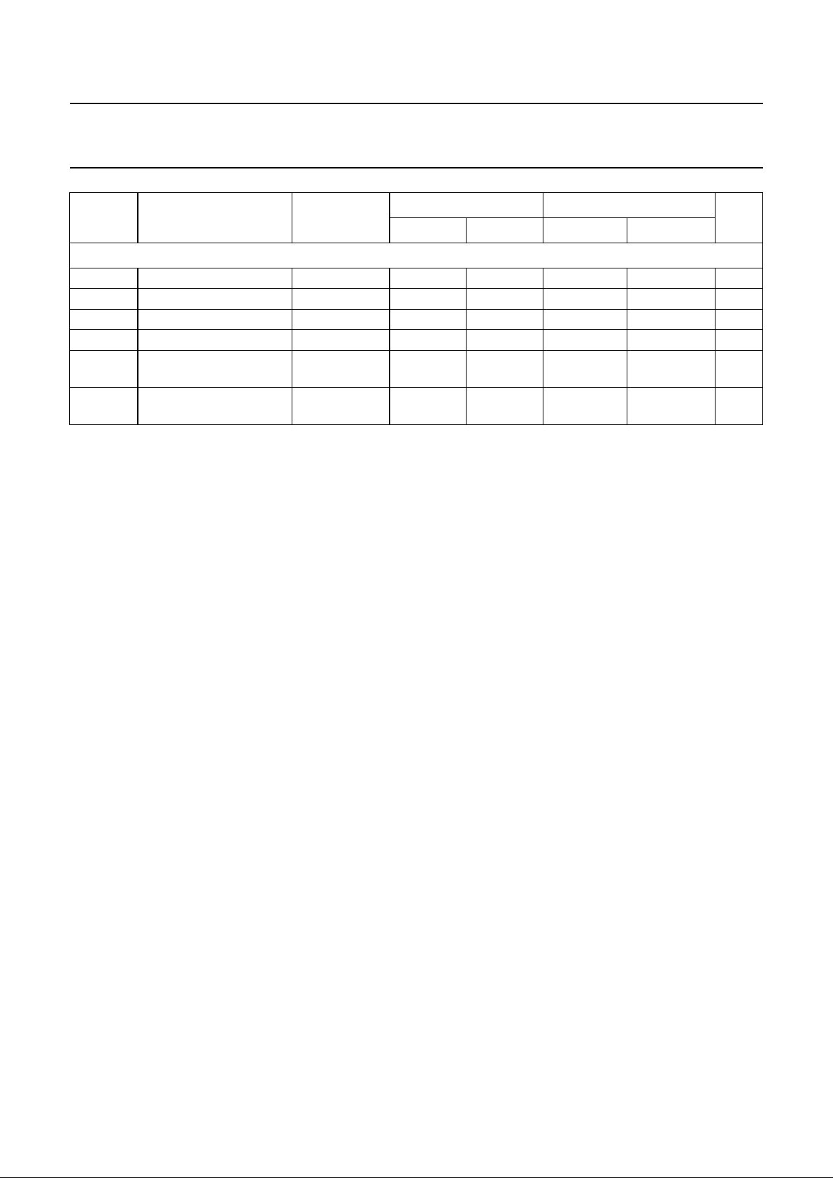
Philips Semiconductors Preliminary specification
Digital servo processor and Compact Disc
SAA7370A
decoder (CD7)
SYMBOL PARAMETER CONDITIONS
WRITE MODE (CL= 20 pF)
t
sD
t
hD
t
sCL
t
hCL
t
dPLP
t
dWZ
Notes
1. The 4-wire bus mode microprocessor interface timing for writing to registers 0 to F, and reading Q-channel subcode
and decoder status, is a function of the overspeed factor ‘n’. In the lock-to-disc mode the maximum data rate is lower.
2. Negative set-up time means that the data may change after clock transition.
3. If a 16.9344 MHz crystal is used and SELPLL = 1 then the timings are divided-by-2.
4. If a 16.9344 MHz crystal is used and SELPLL = 0 then the timings are divided-by-2 until the microcontroller has
written x1xx to register B.
set-up time SDA to SCL 0 − 0 − ns
hold time SCL to SDA 950 − 950 − ns
set-up time SCL to SILD 480 − 480 − ns
hold time SILD to SCL 120 − 120 − ns
delay between two
SILD pulses
delay time SDA
high-impedance to SILD
NORMAL MODE LOCK-TO-DISC MODE
UNIT
MIN. MAX. MIN. MAX.
70 − 70 −µs
0 − 0 − ns
1995 Nov 29 51
Page 52
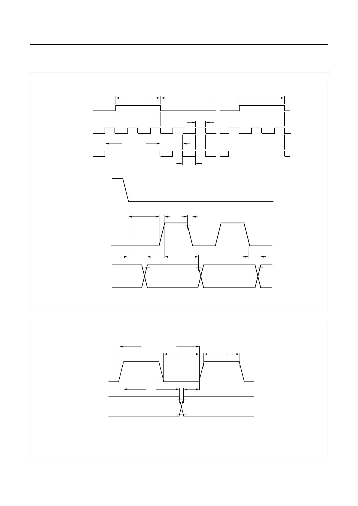
Philips Semiconductors Preliminary specification
Digital servo processor and Compact Disc
decoder (CD7)
0.8 V
t
W(SBSY)
t
W(SFSY)
t
d(SFSY−RCK)
t
d(SFSY−SUB)
t
cy(frame)
t
r
t
h(RCK−SUB)
handbook, full pagewidth
SBSY
SFSY
(4-wire mode)
SFSY
(3-wire mode)
SFSY
RCK
t
SFSYL
t
SFSYH
t
f
V
DD
– 0.8 V
T
cy(block)
t
d(RCK−SUB)
SAA7370A
0.8 V
SUB
SCLK
WCLK
DATA
EF
Fig.31 Subcode interface timing diagram.
clock period T
t
h
cy
t
CL
t
su
V – 0.8 V
DD
0.8 V
t
CH
V – 0.8 V
DD
0.8 V
MBG407
V
DD
0.8 V
– 0.8 V
MBG414
Fig.32 I2S-bus timing diagram.
1995 Nov 29 52
Page 53
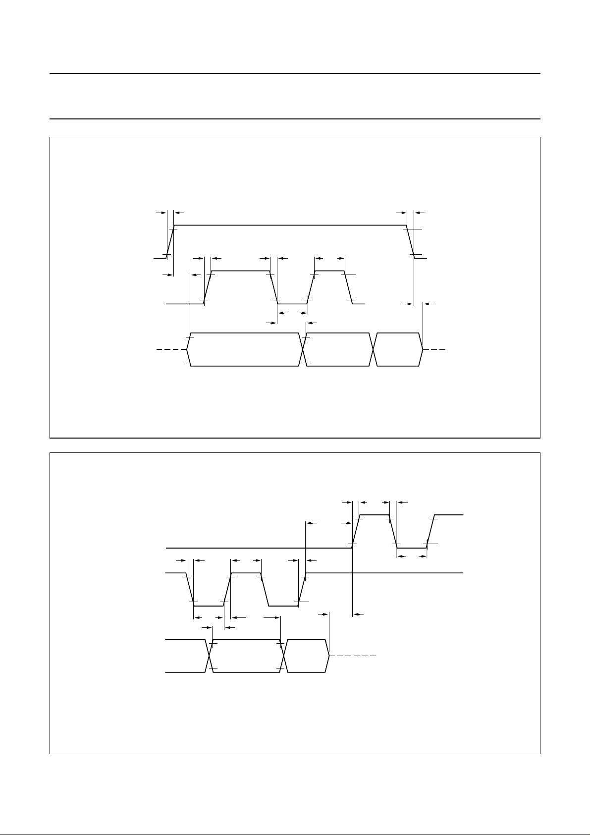
Philips Semiconductors Preliminary specification
Digital servo processor and Compact Disc
decoder (CD7)
t
r
RAB
SCL
SDA (SAA7370A)
high-impedance
t
dRD
t
r
t
f
t
CL
t
PD
V – 0.8 V
0.8 V
DD
SAA7370A
t
f
V – 0.8 V
DD
t
CH
V – 0.8 V
DD
0.8 V
0.8 V
t
dRZ
MBG774
Fig.33 4-wire bus microcontroller timing; read mode (Q-channel subcode and decoder status information).
handbook, full pagewidth
RAB
SCL
SDA
(microcontroller)
t
suD
t
f
t
CL
t
CH
t
V – 0.8 V
DD
0.8 V
hD
t
r
t
suCR
t
r
V – 0.8 V
DD
0.8 V
t
dWZ
high-impedance
t
CH
t
f
V – 0.8 V
DD
t
0.8 V
CL
MBG405
Fig.34 4-wire bus microcontroller timing; write mode (registers 0 to F).
1995 Nov 29 53
Page 54
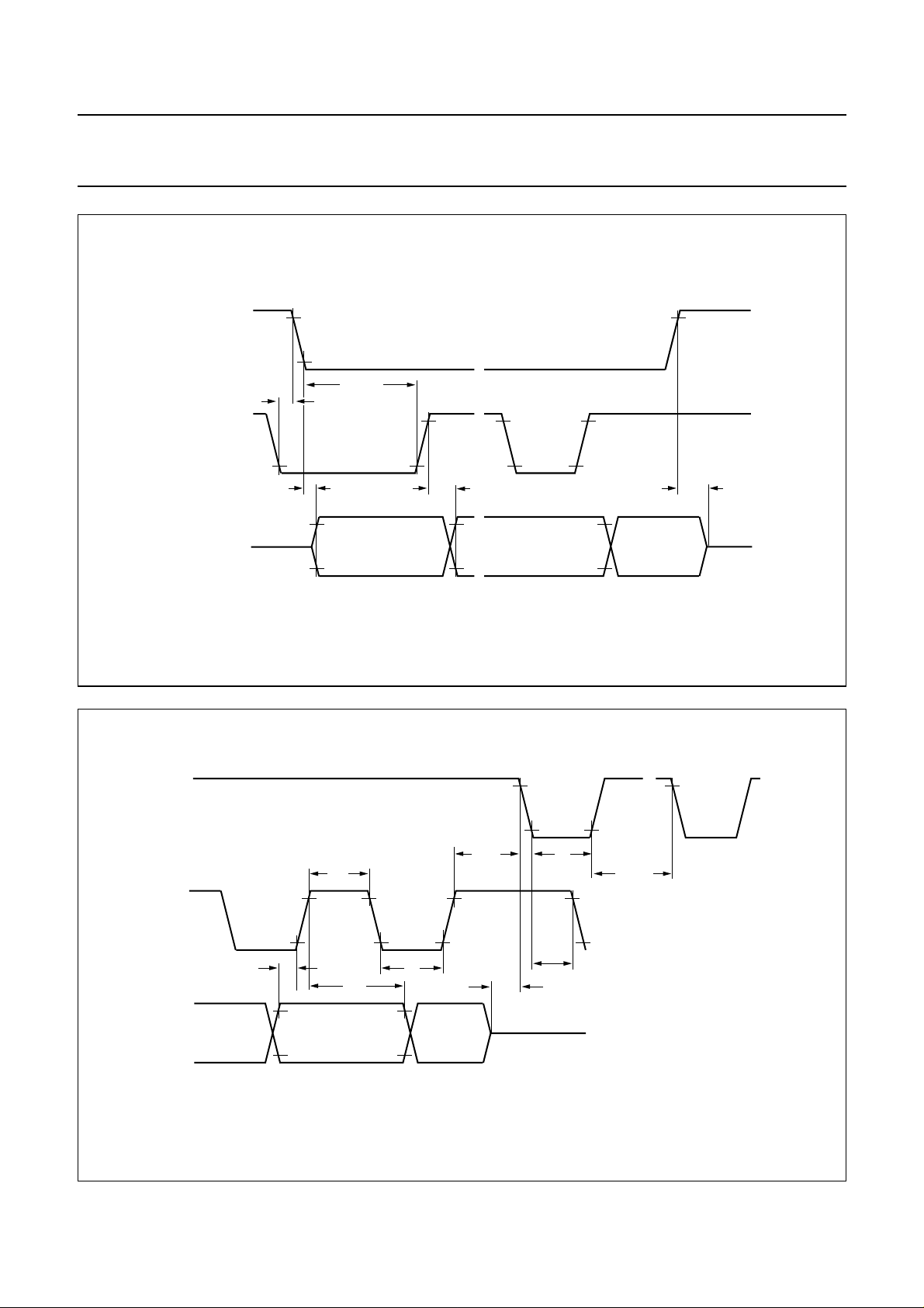
Philips Semiconductors Preliminary specification
Digital servo processor and Compact Disc
decoder (CD7)
handbook, full pagewidth
SILD
0.8 V
t
hCLR
t
sCLR
V
– 0.8 V
DD
SCL
0.8 V
t
PD
SDA
(SAA7370A)
t
dLD
V
– 0.8 V
DD
0.8 V
SAA7370A
V
– 0.8 V
DD
t
dLZ
MBG777
handbook, full pagewidth
SILD
SCL
SDA
(microcontroller)
Fig.35 4-wire bus microcontroller timing; read mode (servo commands).
V
- 0.8 V
DD
0.8 V
t
hCL
t
L
t
dPLP
V
– 0.8 V
DD
V
DD
t
sD
– 0.8 V
0.8 V
0.8 V
t
t
H
t
t
hD
L
sCL
t
dWZ
MBG416
Fig.36 4-wire bus microcontroller timing; write mode (servo commands).
1995 Nov 29 54
Page 55
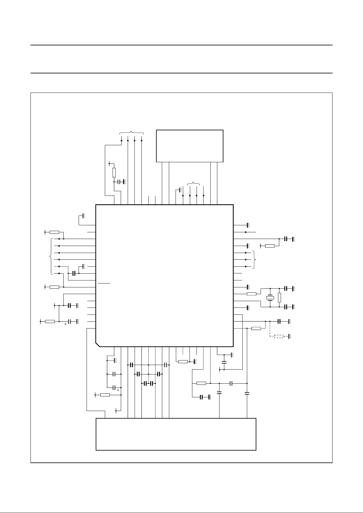
Philips Semiconductors Preliminary specification
Digital servo processor and Compact Disc
decoder (CD7)
13 APPLICATION INFORMATION
to DAC
or CD-ROM
block decoder
DD
V
2.2 Ω
100 nF
484746454443424140393837363534
V3V4V5
EF
DATA
D2
KILL
D3
VRLD4R1R2
SSD2
V
SAA7370A
refT
I
10111213141516
+V
4.7
kΩ
interface
microcontroller
4.7
kΩ
+V
DD
V
+V
2.2 Ω
100
33 µF
100
nF
SCLK
WCLK
DDD2(P)
SSD3
49
V
V
CL4
SDA
SCL
RAB
53 52 51 50
SILD
nF
n.c.
SSD4
V
RESET
STATUS
DDD3C
V
C2FAIL
CFLG
V1
63 62 61 60 59 58 57 56 55 54
V2
64
SSA1VDDA1
V
D1
123456789
MOTOR
INTERFACE
to CD
SUB
RCK
SSA2
VRHV
graphics
SFSY
SBSY
SELPLL
ISLICE
33
MOTO2
MOTO1
SSA3
HFIN
V
SSD1
V
DOBM
DDD1(P)
V
TEST3
SL
FO
RA
CL11
CL16
TEST2
CROUT
CRIN
TEST1
DDA2
V
ref
I
HFREF LDON
SAA7370A
MBG767
to DOBM
transformer
DD
V
28 29 30 31 32
to power
amplifiers
(1)
18 19 20 21 22 23 24 25 26 27
17
22 kΩ
100 nF
2.2 Ω
(pin 18) and ground.
handbook, full pagewidth
ref
Fig.37 Typical application diagram.
nF
100
(2)
nF
100
µF
DDA
V
220 pF
220 pF
220 pF
33
+V
Ω
2.2
220 pF
220 pF
220 pF
AND
MECHANISM
HF AMPLIFIER
1995 Nov 29 55
270
nF
kΩ
22
kΩ
nF
100
DDA
V
1 nF
100
10
pF
1 nF
(1) For crystal oscillator see Figs 3 and 4.
(2) For n = 8 applications an additional resistor (value tbf) should be added between I
Page 56
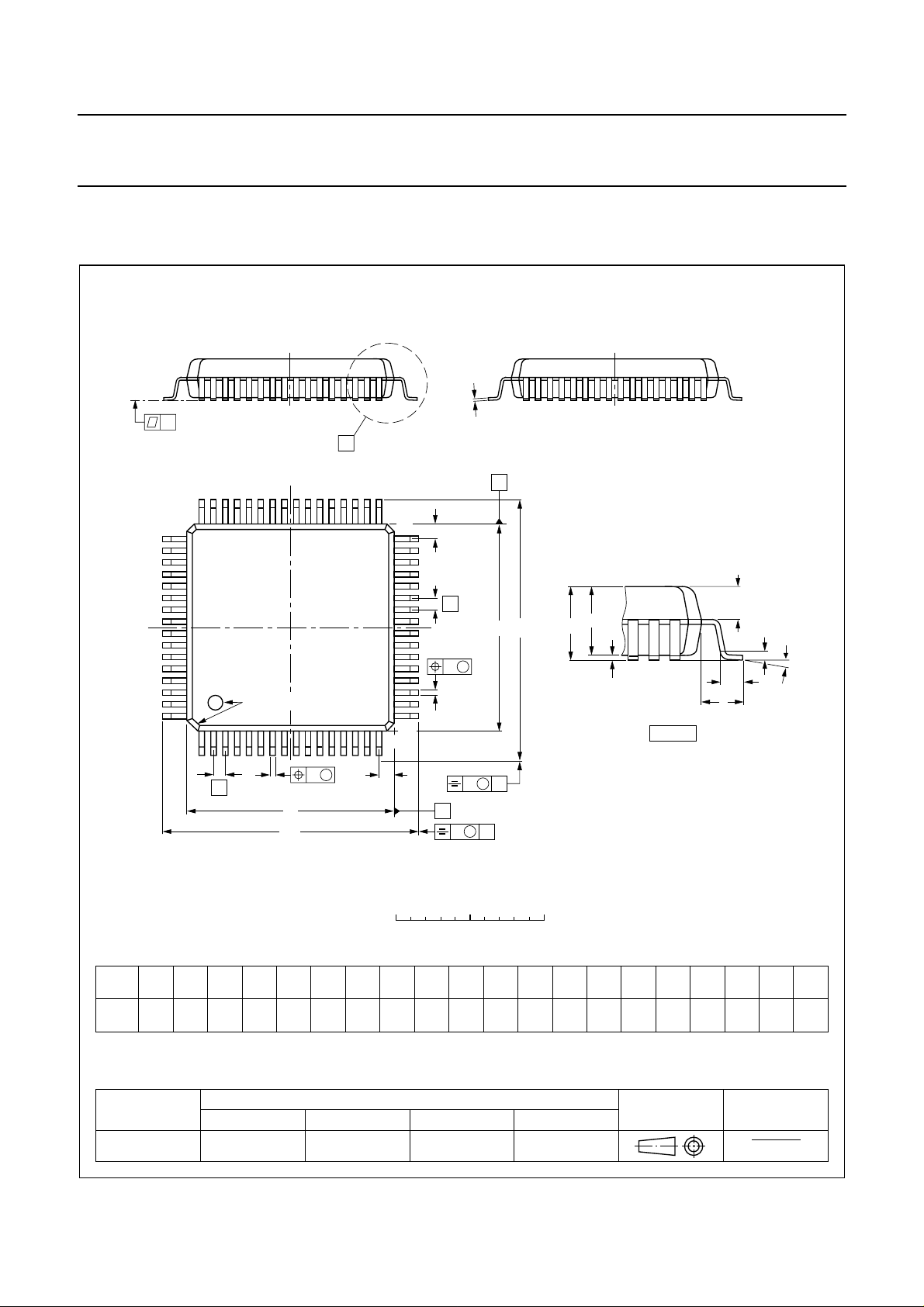
Philips Semiconductors Preliminary specification
Digital servo processor and Compact Disc
decoder (CD7)
14 PACKAGE OUTLINE
QFP64: plastic quad flat package; 64 leads (lead length 1.6 mm); body 14 x 14 x 2.7 mm
c
y
X
A
48 33
49
32
Z
E
SAA7370A
SOT393-1
e
w M
b
pin 1 index
64
1
w M
b
0.25
p
D
H
D
cE
p
0.45
0.23
0.30
0.13
e
DIMENSIONS (mm are the original dimensions)
mm
A
max.
3.00
0.25
0.10
2.75
2.55
UNIT A1A2A3b
Note
1. Plastic or metal protrusions of 0.25 mm maximum per side are not included.
16
Z
D
0 5 10 mm
(1)
(1) (1)(1)
D
14.1
14.1
13.9
13.9
p
17
B
v M
scale
eH
H
17.45
0.8
16.95
v M
D
E
A
B
E
17.45
16.95
A
H
E
LLpQZywv θ
A
1.03
0.73
2
A
1
detail X
1.4
1.1
0.16 0.100.161.60
Q
(A )
3
θ
L
p
L
Z
E
D
1.2
0.8
o
7
o
0
1.2
0.8
OUTLINE
VERSION
SOT393-1 MS-022
IEC JEDEC EIAJ
REFERENCES
1995 Nov 29 56
EUROPEAN
PROJECTION
ISSUE DATE
94-06-22
96-05-21
Page 57

Philips Semiconductors Preliminary specification
Digital servo processor and Compact Disc
decoder (CD7)
15 SOLDERING
15.1 Introduction
There is no soldering method that is ideal for all IC
packages. Wave soldering is often preferred when
through-hole and surface mounted components are mixed
on one printed-circuit board. However, wave soldering is
not always suitable for surface mounted ICs, or for
printed-circuits with high population densities. In these
situations reflow soldering is often used.
This text gives a very brief insight to a complex technology.
A more in-depth account of soldering ICs can be found in
“IC Package Databook”
our
15.2 Reflow soldering
Reflow soldering techniques are suitable for all QFP
packages.
The choice of heating method may be influenced by larger
plastic QFP packages (44 leads, or more). If infrared or
vapour phase heating is used and the large packages are
not absolutely dry (less than 0.1% moisture content by
weight), vaporization of the small amount of moisture in
them can cause cracking of the plastic body. For more
information, refer to the Drypack chapter in our
Reference Handbook”
Reflow soldering requires solder paste (a suspension of
fine solder particles, flux and binding agent) to be applied
to the printed-circuit board by screen printing, stencilling or
pressure-syringe dispensing before package placement.
Several techniques exist for reflowing; for example,
thermal conduction by heated belt. Dwell times vary
between 50 and 300 seconds depending on heating
method. Typical reflow temperatures range from
215 to 250 °C.
Preheating is necessary to dry the paste and evaporate
the binding agent. Preheating duration: 45 minutes at
45 °C.
(order code 9398 652 90011).
“Quality
(order code 9397 750 00192).
SAA7370A
15.3 Wave soldering
Wave soldering is not recommended for QFP packages.
This is because of the likelihood of solder bridging due to
closely-spaced leads and the possibility of incomplete
solder penetration in multi-lead devices.
If wave soldering cannot be avoided, the following
conditions must be observed:
• A double-wave (a turbulent wave with high upward
pressure followed by a smooth laminar wave)
soldering technique should be used.
• The footprint must be at an angle of 45° to the board
direction and must incorporate solder thieves
downstream and at the side corners.
Even with these conditions, do not consider wave
soldering the following packages: QFP52 (SOT379-1),
QFP100 (SOT317-1), QFP100 (SOT317-2),
QFP100 (SOT382-1) or QFP160 (SOT322-1).
During placement and before soldering, the package must
be fixed with a droplet of adhesive. The adhesive can be
applied by screen printing, pin transfer or syringe
dispensing. The package can be soldered after the
adhesive is cured.
Maximum permissible solder temperature is 260 °C, and
maximum duration of package immersion in solder is
10 seconds, if cooled to less than 150 °C within
6 seconds. Typical dwell time is 4 seconds at 250 °C.
A mildly-activated flux will eliminate the need for removal
of corrosive residues in most applications.
15.4 Repairing soldered joints
Fix the component by first soldering two diagonallyopposite end leads. Use only a low voltage soldering iron
(less than 24 V) applied to the flat part of the lead. Contact
time must be limited to 10 seconds at up to 300 °C. When
using a dedicated tool, all other leads can be soldered in
one operation within 2 to 5 seconds between
270 and 320 °C.
1995 Nov 29 57
Page 58
Philips Semiconductors Preliminary specification
Digital servo processor and Compact Disc
SAA7370A
decoder (CD7)
16 DEFINITIONS
Data sheet status
Objective specification This data sheet contains target or goal specifications for product development.
Preliminary specification This data sheet contains preliminary data; supplementary data may be published later.
Product specification This data sheet contains final product specifications.
Short-form specification The data in this specification is extracted from a full data sheet with the same type
number and title. For detailed information see the relevant data sheet or data handbook.
Limiting values
Limiting values given are in accordance with the Absolute Maximum Rating System (IEC 134). Stress above one or
more of the limiting values may cause permanent damage to the device. These are stress ratings only and operation
of the device at these or at any other conditions above those given in the Characteristics sections of the specification
is not implied. Exposure to limiting values for extended periods may affect device reliability.
Application information
Where application information is given, it is advisory and does not form part of the specification.
17 LIFE SUPPORT APPLICATIONS
These products are not designed for use in life support appliances, devices, or systems where malfunction of these
products can reasonably be expected to result in personal injury. Philips customers using or selling these products for
use in such applications do so at their own risk and agree to fully indemnify Philips for any damages resulting from such
improper use or sale.
2
18 PURCHASE OF PHILIPS I
Purchase of Philips I
components in the I2C system provided the system conforms to the I2C specification defined by
Philips. This specification can be ordered using the code 9398 393 40011.
C COMPONENTS
2
C components conveys a license under the Philips’ I2C patent to use the
1995 Nov 29 58
Page 59

Philips Semiconductors Preliminary specification
Digital servo processor and Compact Disc
decoder (CD7)
NOTES
SAA7370A
1995 Nov 29 59
Page 60

Philips Semiconductors – a worldwide company
Argentina: IEROD, Av. Juramento 1992 - 14.b, (1428)
BUENOS AIRES, Tel. (541)786 7633, Fax. (541)786 9367
Australia: 34 Waterloo Road, NORTH RYDE, NSW 2113,
Tel. (02)805 4455, Fax. (02)805 4466
Austria: Triester Str. 64, A-1101 WIEN, P.O. Box 213,
Tel. (01)60 101-1236, Fax. (01)60 101-1211
Belgium: Postbus 90050, 5600 PB EINDHOVEN, The Netherlands,
Tel. (31)40-2783749, Fax. (31)40-2788399
Brazil: Rua do Rocio 220 - 5
CEP: 04552-903-SÃO PAULO-SP, Brazil.
P.O. Box 7383 (01064-970),
Tel. (011)821-2333, Fax. (011)829-1849
Canada: PHILIPS SEMICONDUCTORS/COMPONENTS:
Tel. (800) 234-7381, Fax. (708) 296-8556
Chile: Av. Santa Maria 0760, SANTIAGO,
Tel. (02)773 816, Fax. (02)777 6730
China/Hong Kong: 501 Hong Kong Industrial Technology Centre,
72 Tat Chee Avenue, Kowloon Tong, HONG KONG,
Tel. (852)2319 7888, Fax. (852)2319 7700
Colombia: IPRELENSO LTDA, Carrera 21 No. 56-17,
77621 BOGOTA, Tel. (571)249 7624/(571)217 4609,
Fax. (571)217 4549
Denmark: Prags Boulevard 80, PB 1919, DK-2300
COPENHAGEN S, Tel. (45)32 88 26 36, Fax. (45)31 57 19 49
Finland: Sinikalliontie 3, FIN-02630 ESPOO,
Tel. (358)0-615 800, Fax. (358)0-61580 920
France: 4 Rue du Port-aux-Vins, BP317,
92156 SURESNES Cedex,
Tel. (01)4099 6161, Fax. (01)4099 6427
Germany: P.O. Box 10 63 23, 20043 HAMBURG,
Tel. (040)3296-0, Fax. (040)3296 213.
Greece: No. 15, 25th March Street, GR 17778 TAVROS,
Tel. (01)4894 339/4894 911, Fax. (01)4814 240
India: Philips INDIA Ltd, Shivsagar Estate, A Block,
Dr. Annie Besant Rd. Worli, Bombay 400 018
Tel. (022)4938 541, Fax. (022)4938 722
Indonesia: Philips House, Jalan H.R. Rasuna Said Kav. 3-4,
P.O. Box 4252, JAKARTA 12950,
Tel. (021)5201 122, Fax. (021)5205 189
Ireland: Newstead, Clonskeagh, DUBLIN 14,
Tel. (01)7640 000, Fax. (01)7640 200
Italy: PHILIPS SEMICONDUCTORS S.r.l.,
Piazza IV Novembre 3, 20124 MILANO,
Tel. (0039)2 6752 2531, Fax. (0039)2 6752 2557
Japan: Philips Bldg 13-37, Kohnan 2-chome, Minato-ku, TOKYO 108,
Tel. (03)3740 5130, Fax. (03)3740 5077
Korea: Philips House, 260-199 Itaewon-dong,
Yongsan-ku, SEOUL, Tel. (02)709-1412, Fax. (02)709-1415
Malaysia: No. 76 Jalan Universiti, 46200 PETALING JAYA,
SELANGOR, Tel. (03)750 5214, Fax. (03)757 4880
Mexico: 5900 Gateway East, Suite 200, EL PASO, TX 79905,
Tel. 9-5(800)234-7381, Fax. (708)296-8556
th
floor, Suite 51,
Netherlands: Postbus 90050, 5600 PB EINDHOVEN, Bldg. VB,
Tel. (040)2783749, Fax. (040)2788399
New Zealand: 2 Wagener Place, C.P.O. Box 1041, AUCKLAND,
Tel. (09)849-4160, Fax. (09)849-7811
Norway: Box 1, Manglerud 0612, OSLO,
Tel. (022)74 8000, Fax. (022)74 8341
Pakistan: Philips Electrical Industries of Pakistan Ltd.,
Exchange Bldg. ST-2/A, Block 9, KDA Scheme 5, Clifton,
KARACHI 75600, Tel. (021)587 4641-49,
Fax. (021)577035/5874546
Philippines: PHILIPS SEMICONDUCTORS PHILIPPINES Inc.,
106 Valero St. Salcedo Village, P.O. Box 2108 MCC, MAKATI,
Metro MANILA, Tel. (63) 2 816 6380, Fax. (63) 2 817 3474
Portugal: PHILIPS PORTUGUESA, S.A.,
Rua dr. António Loureiro Borges 5, Arquiparque - Miraflores,
Apartado 300, 2795 LINDA-A-VELHA,
Tel. (01)4163160/4163333, Fax. (01)4163174/4163366
Singapore: Lorong 1, Toa Payoh, SINGAPORE 1231,
Tel. (65)350 2000, Fax. (65)251 6500
South Africa: S.A. PHILIPS Pty Ltd.,
195-215 Main Road Martindale, 2092 JOHANNESBURG,
P.O. Box 7430, Johannesburg 2000,
Tel. (011)470-5911, Fax. (011)470-5494
Spain: Balmes 22, 08007 BARCELONA,
Tel. (03)301 6312, Fax. (03)301 42 43
Sweden: Kottbygatan 7, Akalla. S-164 85 STOCKHOLM,
Tel. (0)8-632 2000, Fax. (0)8-632 2745
Switzerland: Allmendstrasse 140, CH-8027 ZÜRICH,
Tel. (01)488 2211, Fax. (01)481 77 30
Taiwan: PHILIPS TAIWAN Ltd., 23-30F, 66, Chung Hsiao West
Road, Sec. 1. Taipeh, Taiwan ROC, P.O. Box 22978,
TAIPEI 100, Tel. (886) 2 382 4443, Fax. (886) 2 382 4444
Thailand: PHILIPS ELECTRONICS (THAILAND) Ltd.,
209/2 Sanpavuth-Bangna Road Prakanong,
Bangkok 10260, THAILAND,
Tel. (66) 2 745-4090, Fax. (66) 2 398-0793
Turkey:Talatpasa Cad. No. 5, 80640 GÜLTEPE/ISTANBUL,
Tel. (0212)279 27 70, Fax. (0212)282 67 07
Ukraine: Philips UKRAINE, 2A Akademika Koroleva str., Office 165,
252148 KIEV, Tel.380-44-4760297, Fax. 380-44-4766991
United Kingdom: Philips Semiconductors LTD.,
276 Bath Road, Hayes, MIDDLESEX UB3 5BX,
Tel. (0181)730-5000, Fax. (0181)754-8421
United States:811 East Arques Avenue, SUNNYVALE,
CA 94088-3409, Tel. (800)234-7381, Fax. (708)296-8556
Uruguay: Coronel Mora 433, MONTEVIDEO,
Tel. (02)70-4044, Fax. (02)92 0601
Internet: http://www.semiconductors.philips.com/ps/
For all other countries apply to: Philips Semiconductors,
International Marketing and Sales, Building BE-p,
P.O. Box 218, 5600 MD EINDHOVEN, The Netherlands,
Telex 35000 phtcnl, Fax. +31-40-2724825
SCD46 © Philips Electronics N.V. 1995
All rights are reserved. Reproduction in whole or in part is prohibited without the
prior written consent of the copyright owner.
The information presented in this document does not form part of any quotation
or contract, is believed to be accurate and reliable and may be changed without
notice. No liability will be accepted by the publisher for any consequence of its
use. Publication thereof does not convey nor imply any license under patent- or
other industrial or intellectual property rights.
Printed in The Netherlands
513061/1100/01/pp60 Date of release: 1995 Nov 29
Document order number: 9397 750 00485
 Loading...