

Page 1
INTEGRATED CIRCUITS
DATA SH EET
SAA7367
Bitstream conversion ADC for
digital audio systems
Product specification
Supersedes data of 1996 Jun 17
File under Integrated Circuits, IC01
1998 Nov 17
Page 2
Philips Semiconductors Product specification
Bitstream conversion ADC for
digital audio systems
FEATURES
• Total Harmonic Distortion plus Noise
(THD + N) = −88 dB (0.004%); DR = 93 dB;
S/N = 97 dB
• Simple interfacing to analog inputs
• Small, non-critical PCB layout
• Low pin-out SO24 package (pin-compatible to
SAA7366)
• 4 flexible serial interface modes
• 4.5 to 5.5 V operation
• Standby mode
• Detection of digital signal ≥−1 dB amplitude
• Up to 18 significant bits serial output
• Selectable high-pass filter.
APPLICATIONS
The device is designed for the digital acquisition of analog
audio signals for digital audio systems such as:
• Compact Disc-Recordable (CD-R)
• Audio digital signal processing systems for hi-fi and
musical instrument applications
• Digital Audio Tape (DAT).
SAA7367
GENERAL DESCRIPTION
The SAA7367 is a CMOS low-cost stereo
Analog-to-Digital Converter (ADC) using the Philips
bitstream conversion technique.
QUICK REFERENCE DATA
SYMBOL PARAMETER CONDITIONS MIN. TYP. MAX. UNIT
V
DDD
I
DDD
V
DDA
I
DDA
f
BCK
f
s
THD + N total harmonic distortion plus
digital supply voltage 4.5 5.0 5.5 V
digital supply current − 17 − mA
analog supply voltage 4.5 5.0 5.5 V
analog supply current − 13 − mA
clock input frequency 4.60 12.288 12.8 MHz
sample rate 18 48 50 kHz
at 0 dB input −−88 −80 dB
noise
DR dynamic range at −60 dB 90 93 − dB
S/N signal-to-noise ratio − 97 − dB
ORDERING INFORMATION
TYPE
NUMBER
NAME DESCRIPTION VERSION
PACKAGE
SAA7367 SO24 plastic small outline package; 24 leads; body width 7.5 mm SOT137-1
1998 Nov 17 2
Page 3
Philips Semiconductors Product specification
Bitstream conversion ADC for
digital audio systems
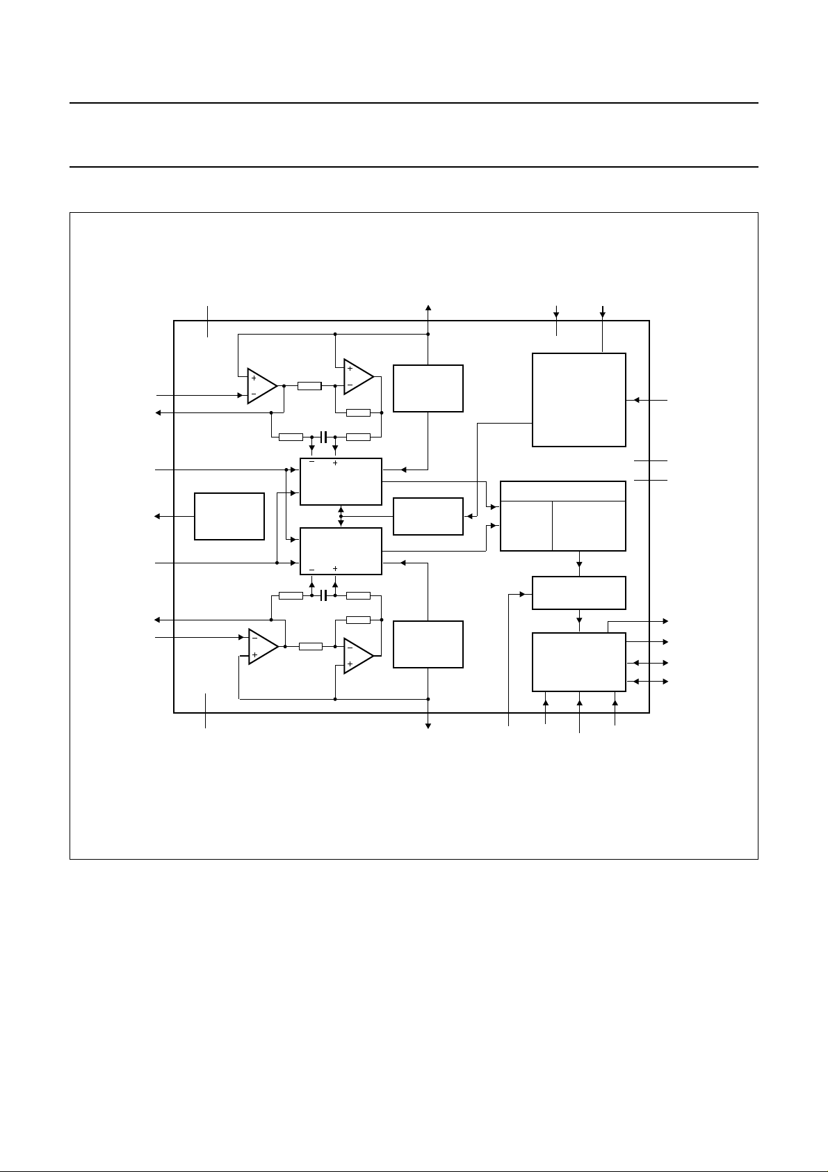
BLOCK DIAGRAM
V
16
17
19
REFERENCE
14
GENERATOR
18
20
21
SSA
operational
amplifier
CURRENT
operational
amplifier
23
handbook, full pagewidth
BIR
BOR
V
DACP
I
ref
V
DACN
BOL
BIL
operational
amplifier
SIGMA-
DELTA
MODULATOR
SIGMA-
DELTA
MODULATOR
operational
amplifier
V
refR
REFERENCE
VOLT AGE
GENERATOR
TIMING
GENERATOR
REFERENCE
VOLT AGE
GENERATOR
22
SAA7367
TESTB
DECIMATION FILTER
STAGE 1
COMB
FILTER
SERIAL OUTPUT
11 1
STDB
CLOCK
GENERATION
AND
CONTROL
STAGE 2
3 HALF-BAND
FILTERS
HIGH-PASS
FILTER
INTERFACE
24
10
SAA7367
2121513
4
CKIN
5
V
DDD
6
V
SSD
3
OVLD
7
SDO
8
SWS
9
SCK
V
DDA
Fig.1 Block diagram.
1998 Nov 17 3
HPEN
V
refL
TEST1
SLAVE
SFOR
MGE645
Page 4
Philips Semiconductors Product specification
Bitstream conversion ADC for
SAA7367
digital audio systems
PINNING
SYMBOL PIN DESCRIPTION
SFOR 1 TTL level input; in normal mode this input selects the serial interface output format; output
format is selected as follows:
SFOR = HIGH selects Format 1
SFOR = LOW selects Format 2 (similar to I
STDB 2 schmitt-trigger input; in normal mode, this input is used to select standby mode:
STDB = HIGH selects normal operation
STDB = LOW selects standby mode (low power consumption)
OVLD 3 TTL level output; in normal mode this output indicates whether the internal digital signal is
within 1 dB of maximum; if so, the output will go HIGH for 131072 clock cycles (approximately
11 ms); in standby mode this output is forced LOW
CKIN 4 CMOS level input; system clock input; nominally clocked at 256f
V
V
DDD
SSD
5 digital supply voltage (4.5 to 5.5 V)
6 digital ground
SDO 7 TTL level output (3-state); in normal mode this pin outputs data from the serial interface; in
standby mode, this output is high impedance
SWS 8 TTL level input/output; serial interface word select signal; in master mode (SLAVE = LOW),
this pin outputs the serial interface word select signal; in slave mode (SLAVE = HIGH), this pin
is the word select input to the serial interface; in standby mode (STDB = LOW) this pin is
always an input (high impedance); for polarity: see Table 1
SCK 9 TTL level input/output; in master mode (SLAVE = LOW) the pin outputs the serial interface bit
clock; in slave mode (SLAVE = HIGH) this pin is the input for the external bit clock; data on
SDO is clocked out on the HIGH-to-LOW transition of SCK; the data is valid on the
LOW-to-HIGH transition
TEST1 10 Test1; TTL level input with internal pull-down; in slave mode (slave = HIGH), this pin is used
to select extra serial interface formats (see Table 2)
HPEN 11 TTL level input; this input is used to enable the internal high-pass filter when HIGH; in
scan-test mode (TESTB = LOW and TEST1 = LOW) this pin functions as ‘scan chain c’ input
TESTB 12 TestB; CMOS level input with internal pull-up; in normal applications, this input should be left
HIGH
V
I
V
SSA
ref
refR
13 analog ground; this pin is internally connected to VSS via the on-chip substrate contacts
14 current reference generator output; 33 kΩ in parallel with 22 nF is connected from this pin to
V
SSA
15 right channel analog reference output voltage (1⁄2V
BIR 16 buffer operational amplifier inverting input for right channel
BOR 17 buffer operational amplifier output for right channel
V
DACN
V
DACP
18 negative 1-bit DAC reference voltage input, connected to 0 V
19 positive 1-bit DAC reference voltage input, connected to +5 V
BOL 20 buffer operational amplifier output for left channel
BIL 21 buffer operational amplifier inverting input for left channel
V
V
refL
DDA
22 left channel analog reference output voltage (1⁄2V
23 analog supply voltage (4.5 to 5.5 V)
2
S)
s
)
DDA
)
DDA
1998 Nov 17 4
Page 5

Philips Semiconductors Product specification
Bitstream conversion ADC for
digital audio systems
SYMBOL PIN DESCRIPTION
SLAVE 24 TTL level input; used to select the serial interface operating mode:
SLAVE = HIGH selects slave mode
SLAVE = LOW selects master mode
Table 1 SWS polarity
CONDITIONS
SLAVE AND TEST1 SWS SFOR
SLAVE = LOW or TEST1 = LOW LOW LOW left data
LOW HIGH right data
SLAVE = HIGH and TEST1 = HIGH LOW LOW right data
LOW HIGH left data
Table 2 Selection of serial interface formats via TEST1
CONDITIONS
SELECTED FORMAT
SFOR TEST1
HIGH LOW format 1
HIGH format 3
LOW LOW format 2
HIGH format 4
SAA7367
POLARITY
handbook, halfpage
SFOR
1
STDB
2
OVLD
3
CKIN
4
V
5
DDD
V
6
SSD
SDO
SWS
SCK
TEST1
HPEN
TESTB
7
8
9
10
11
12
SAA7367
MGE644
Fig.2 Pin configuration.
FUNCTIONAL DESCRIPTION
General
SLAVE
24
V
23
DDA
V
22
refL
BIL
21
BOL
20
The SAA7367 is a bitstream conversion CMOS ADC for
digital audio systems. The conversion is achieved using a
third-order Sigma-Delta Modulator (SDM), running at
128 times the output sample frequency (f
). The high
s
oversampling ratio greatly simplifies the design of the
analog input anti-alias filter. In most events, the internal
buffer operational amplifier, configured as a low-pass filter,
19
V
DACP
V
18
DACN
17
BOR
BIR
16
V
15
refR
I
14
ref
V
13
SSA
will suffice. The 1-bit code from the SDM is filtered and
down-sampled (decimated) to 1fs by Finite Impulse
Response (FIR) filters. An optional I2R high-pass filter is
provided to remove DC, if required. The device has been
designed with ease of use, low board area and low
application costs in mind.
Clock frequency
The external clock input on pin CKIN runs at 256f
, which
s
can range from 18 to 50 kHz.
1998 Nov 17 5
Page 6

Philips Semiconductors Product specification
Bitstream conversion ADC for
digital audio systems
Input buffer
Two input buffers are provided, one for each channel, for
signal amplitude matching, signal buffering and anti-alias
filter purposes. These are configured for inverting use.
Access is provided by pins BIL, BIR (inverting inputs) and
BOL, BOR (outputs), for left and right channels
respectively. By the choice of feedback component values,
the application signal amplitude can be matched to the
requirements of the ADC.
Typically, the operational amplifiers are configured as
low-pass filters with a gain of 1 and a pole at
approximately 5f
Remark: the complete ADC is non-inverting. Hence, a
positive DC input (referenced to V
digital output.
Input level
The overall system gain is proportional V
accurately the potential difference between the DAC
reference voltages (V
convenience, the ADC input signal amplitude is defined as
that amplitude seen on BOL or BOR, the operational
amplifier outputs (i.e. the input to the SDM). Also, the 0 dB
input level is defined as that which gives a −1 dB (actually
−1.12 dB) digital output, relative to full-scale swing. This
reduced gain provides headroom to accommodate small
random DC offsets, without causing the digital output to
clip.
Hence:
V
0dB()
I
.
s
) and (V
VDACP
V
=
-------------------------------------------------------
–()
VDACPVVDACN
5V(RMS)
) will yield a positive
ref
, or more
DDA
). For
VDACN
SAA7367
Input signals in the range 0 to 1 dB may or may not be
clipped, depending on the values of DC dither and small
random offsets in the analog circuitry.
When using the recommended application circuitry,
clipping will initially be observed on negative peaks, due to
the use of negative DC dither.
The maximum level of overload that can be safely
tolerated is application circuit dependent. In the case of the
recommended circuit, the following applies: the inverting
operational amplifier inputs BIL and BIR are protected
from excessive voltages (currents) by diodes to V
V
. These have absolute maximum ratings of
SSA
Id= ±20 mA, with a safe practical limit of ±2 mA.
Given the input resistor of 10 kΩ, ±2 mA diode current and
the operation of the operational amplifier, a maximum
signal (applied to the input resistor) of ±30 V can be
handled safely. This level represents an overload of 26 dB.
During overload, the in-band portion of the waveform will
be correctly converted. The out-of-band portion will be
limited as previously detailed.
Sigma-Delta Modulator (SDM)
The SAA7367 uses two third-order SDMs with a
quantization noise floor of approximately −104 dB. The
scaling of the feedback has been optimized for stable
operation, even during overload. Thus, with a maximum
signal swing of 0 V to V
on the input, the digital output
DDA
remains well-behaved, i.e. it does not burst into random
oscillation. During overload, the output is simply a clipped
version of the input. The gain of this stage is −4.64 dB.
Decimation filter
DDA
and
The user of the IC should ensure that, when all sources of
signal amplitude variation are taken into account, the
maximum input signal should conform to the 0 dB level.
In the event that the maximum signal level cannot be
pre-determined, e.g. live microphone input, the average
signal level should be set at −10 to −20 dB down. The
exact value will depend on the application and the balance
between headroom and operating Signal-to-Noise Ratio
(SNR).
Behaviour during overload
As previously defined, the maximum input level for normal
operation is 0 dB. If the input level exceeds this value,
clipping may occur. Within the system, excessive
amplitudes are detected after the high-pass filter.
Infringements are limited to the maximum permitted
positive or negative values 217− 1 or −217 respectively.
1998 Nov 17 6
Decimation from 128f
is performed in two stages. The first
s
stage, a comb filter, uses 64 symmetrical coefficients to
implement a 3rd sinx⁄x characteristic. This filter decimates
from 128 to 8fs. The second stage, an FIR filter, consists of
three half-band filters, each decimating by a factor of 2.
The overall characteristics are given in Table 3.
Page 7

Philips Semiconductors Product specification
Bitstream conversion ADC for
digital audio systems
Table 3 Overall filter characteristics
ITEM CONDITION VALUE (dB)
Pass band ripple 0 to 0.45f
0.45 to 0.47f
Stop band >0.55f
Dynamic range 0 to 0.42f
s
s
s
s
Gain DC 3.52
High-pass filter
2
An optional I
R high-pass filter is provided to remove
unwanted DC components. The operation is selected
when HPEN is HIGH and deselected when LOW. The filter
has the characteristics given in Table 4.
Table 4 High-pass filter characteristics
ITEM CONDITION
Pass band ripple none
Pass band gain 0
Droop at 0.00042f
Attenuation at DC at 0.00000036f
Dynamic range 0 to 0.45f
s
s
s
Serial interface
The serial interface provides 2 formats in master mode
and 4 in slave mode (see Figs 3 and 4). Format 2 is similar
to Philips I
2
S. In all modes, the interface provides up to
18 significant bits of output data per channel. During
standby mode (STDB = LOW), all interface pins are in
their high impedance state. On recovery from standby, the
serial data output SDO is held LOW until valid data is
available from the decimation filter. This time depends on
whether the high-pass filter is selected:
HPEN = 0; T = 1024/fs, T = 21.3 ms when fs= 48 kHz
HPEN = 1; T = 12288/fs, T = 256.0 ms when
fs=48kHz
±0.1
−0.5
−60
110
VALUE
(dB)
0.146
>40
>110
SAA7367
Standby mode
The STDB pin activates a power saving mode when the
device function is not required. This pin can also be used
as a chip enable.
On a HIGH-to-LOW transition of the STDB pin, the internal
control circuitry starts a timed power-down sequence. This
takes approximately 32 system clock cycles to complete.
Transitions on STDB that are shorter than 32 clock cycles
may have an indeterminate effect. However, the device
will always recover correctly.
During standby, the following occurs:
• The internal logic clock is disabled
• The serial interface pins are forced to high impedance
• The OVLD output is forced LOW
• The analog circuitry is disabled
• The nominal external analog node voltages are
maintained by a low-power circuit. This feature ensures
a fast recovery from standby mode.
Note: since the serial interface pins are high impedance
during standby, these pins could be wire-ORed with other
serial interface ICs.
On a LOW-to-HIGH transition, the device reverts back to
normal operation. This process takes approximately
256 system clock cycles. Before SDO is enabled, the
output data is forced LOW. SDO remains LOW until good
data is available from the decimation filter
(see Section “Serial interface”).
The STDB pin has a Schmitt-trigger input. A simple
power-on-reset function can be effected using an external
capacitor to V
TEST1
This pin is used to select the serial interface format in slave
mode.
and resistor to VDD.
SS
Overload detection
The OVLD output is used to indicate when the output data,
in either the left or right channel, is greater than −1dB
(actual figure −1.023 dB) of the maximum possible digital
swing. When this condition is detected, the OVLD output is
forced HIGH for at least 512f
cycles (10.6 ms at
s
fs= 48 kHz). This time-out is reset for each infringement.
1998 Nov 17 7
Page 8

Philips Semiconductors Product specification
Bitstream conversion ADC for
SAA7367
digital audio systems
LIMITING VALUES
In accordance with the Absolute Maximum Rating System (IEC 134).
SYMBOL PARAMETER MIN. MAX. UNIT
V
DDA
V
I
I
IK
V
O
I
O
I
DD(tot)
I
SStot
T
amb
T
stg
Note
1. V
SSD
and V
QUALITY SPECIFICATION
analog supply voltage (note 1) −0.5 +6.5 V
DC input voltage −0.5 +6.5 V
DC input clamp diode current −±20 mA
DC output voltage −0.5 VDD+ 0.5 V
DC output source or sink current −±20 mA
total DC supply current −±0.5 A
total DC supply current −±0.5 A
operating ambient temperature −40 +85 °C
storage temperature −65 +150 °C
must be connected to a common potential.
SSA
In accordance with
Handbook”
.
“SNW-FQ-611-E”
. The number of the quality specification can be found in the
“Quality Reference
CHARACTERISTICS
= 4.5 to 5.5 V; V
V
DDD
= 4.5 to 5.5 V; fs= 18 to 50 kHz; T
DDA
= −40 to +85 °C; unless otherwise specified.
amb
SYMBOL PARAMETER CONDITIONS MIN. TYP. MAX. UNIT
Supplies
V
DDD
I
DDD
V
DDA
I
DDA
P
tot
I
stb
P
stb
digital supply voltage 4.5 5 5.5 V
digital supply current fs=48kHz − 17 − mA
analog supply voltage 4.5 5 5.5 V
analog supply current − 13 − mA
total power dissipation fs=48kHz − 150 − mW
standby supply current − 160 −µA
standby power consumption − 800 −µW
Digital part: inputs
SFOR, SLAVE
V
IL
V
IH
I
LI
C
i
AND HPEN
LOW level input voltage −0.5 − +0.8 V
HIGH level input voltage 2.0 − VDD+ 0.5 V
input leakage current −10 − +10 µA
input capacitance −−10 pF
1998 Nov 17 8
Page 9

Philips Semiconductors Product specification
Bitstream conversion ADC for
SAA7367
digital audio systems
SYMBOL PARAMETER CONDITIONS MIN. TYP. MAX. UNIT
CKIN
V
IL
V
IH
I
LI
C
i
TEST1
V
IL
V
IH
R
i
C
i
TESTB
V
IH
R
i
STDB (SCHMITT TRIGGER)
V
IL
V
IH
V
hys
I
LI
C
i
Digital part: inputs/outputs
LOW level input voltage −0.5 − 0.3V
HIGH level input voltage 0.7V
DD
− VDD+ 0.5 V
DD
input leakage current −10 − +10 µA
input capacitance −−10 pF
LOW level input voltage −0.5 − +0.8 V
HIGH level input voltage 2.0 − VDD+ 0.5 V
internal resistance to V
SS
− 50 − kΩ
input capacitance −−10 pF
HIGH level input voltage 0.7V
internal resistance to V
DD
DD
− 50 − kΩ
LOW level input voltage −0.5 − 0.4V
HIGH level input voltage 0.6V
DD
− VDD+ 0.5 V
DD
− VDD+ 0.5 V
hysteresis voltage 200 −− mV
input leakage current −10 − +10 µA
input capacitance −−10 pF
V
V
SWS
AND SCK
V
IL
V
IH
I
Ll
C
i
V
OL
V
OH
C
L
LOW level input voltage −0.5 − +0.8 V
HIGH level input voltage 2.0 VDD+ 0.5 V
3-state leakage current −10 − +10 µA
input capacitance −−10 pF
LOW level output voltage IO= −400 µA −−0.4 V
HIGH level output voltage IO=20µA 2.4 −− V
output load capacitance note 1 −−50 pF
Digital part: outputs
OVLD
V
OL
V
OH
C
L
LOW level output voltage IO= −400 µA −−0.4 V
HIGH level output voltage IO=20µA 2.4 −− V
output load capacitance note 1 −−50 pF
SDO
V
OL
V
OH
I
LI
C
L
LOW level output voltage IO= −400 µA −− 0.4 V
HIGH level output voltage IO=20µA 2.4 −− V
3-state leakage current −10 − +10 µA
output load capacitance note 1 −−50 pF
1998 Nov 17 9
Page 10

Philips Semiconductors Product specification
Bitstream conversion ADC for
SAA7367
digital audio systems
SYMBOL PARAMETER CONDITIONS MIN. TYP. MAX. UNIT
Digital part: timings
CKIN
t
r
t
f
f
i
msr mark-to-space ratio f
Serial Interface master and slave modes (see Figs 5 and 6)
SCK
t
r
t
f
t
L
t
H
f
clk
t
idle
SWS
t
r
t
f
t
L
t
H
f
S
t
d
t
su
SDO
t
h
t
su
t
r
t
f
input rise time −−10 ns
input fall time −−10 ns
input frequency 4.60 − 12.8 MHz
> 32 kHz 40 − 60 %
s
f
≤ 32 kHz 30 − 70 %
s
rise time CL= 50 pF;
−−50 ns
note 1
fall time CL= 50 pF;
−−50 ns
note 1
LOW time T =1⁄64f
HIGH time T =1⁄64f
s
s
clock frequency master mode 64f
slave mode −−64f
burst clock idle time slave mode;
T = 1/f
s
rise time CL= 50 pF;
0.4T − 0.6T ns
0.4T − 0.6T ns
s
64f
s
64f
s
s
0 − 0.5T ns
−−50 ns
note 1
fall time CL= 50 pF;
−−50 ns
note 1
LOW time T = 1/f
HIGH time T = 1/f
s
s
frequency 1f
0.05T 0.5T 0.95T ns
0.05T 0.5T 0.95T ns
s
1f
s
1f
s
delay from SCK master mode −50 − +50 ns
slave mode 50 − ns
set-up time to SCK slave mode 150 −− ns
data output hold time 100 −− ns
data output set-up time 50 −− ns
data output rise time CL= 50 pF;
−−50 ns
note 1
data output fall time CL= 50 pF;
−−50 ns
note 1
MHz
MHz
MHz
1998 Nov 17 10
Page 11

Philips Semiconductors Product specification
Bitstream conversion ADC for
SAA7367
digital audio systems
SYMBOL PARAMETER CONDITIONS MIN. TYP. MAX. UNIT
Analog part at: V
V
AND V
refL
V
O
R
DC
URRENT REFERENCE:I
C
V
O
I
O
V
DACN
V
I
V
DACP
V
I
DD=VDDA
refR
output voltage 0.475V
DC impedance normal mode − 1.3 − kΩ
out put voltage − 0.5V
output current R = 33 kΩ− 76 −µA
input voltage − V
input voltage − V
=5V; T
ref
BUFFER OPERATIONAL AMPLIFIERS: BIL, BOL, BIR AND BOR
V
R
Z
I(off)
L
O
input offset voltage − <10 − mV
load resistance; (drive capability) decoupled to V
output impedance − 100 −Ω
THD + N total harmonic distortion plus
noise
O
VERALL PERFORMANCE (ANALOG IN, DIGITAL OUT)
t
gd
α
sb
group delay time T = 1/f
stop band attenuation f > 0.546 f
DR dynamic range 0 to 20 kHz 90 93 − dB
THD + N total harmonic distortion plus
noise
S/N signal-to-noise ratio A-weighted − 97 − dB
α
cs
channel separation − 92 − dB
G gain note 2 −1.4 −1 −0.8 dB
amb
=25°C
DDA
0.5V
DDA
0.525V
DDA
V
standby mode − 100 − kΩ
− V
DDA
SS
DDA
− 10 − kΩ
ref
− V
− V
f=0to20kHz −−87 − dB
s
s
− 25T − s
60 −− dB
0to20kHz −−88 −80 dB
Notes
1. Load capacitance is valid for master mode only.
2. See also Section “Input level” of Chapter “Functional description”; valid for left or right channel.
1998 Nov 17 11
Page 12

Philips Semiconductors Product specification
Bitstream conversion ADC for
digital audio systems
handbook, full pagewidth
FORMAT 2
FORMAT 1
SCK
SDO
MSB
LEFT DATA
18 CLOCKS
1 STEREO WORD
RIGHT DATA
LEFT DATARIGHT DATA
14 CLOCKS 18 CLOCKS 14 CLOCKS
LSB
MSB
LSB
SAA7367
MSB
MGE647
Fig.3 Serial interface master mode format.
1998 Nov 17 12
Page 13

Philips Semiconductors Product specification
Bitstream conversion ADC for
digital audio systems
handbook, full pagewidth
FORMAT 2
FORMAT 4
idle
SCK
SDO
FORMAT 1
LEFT DATA
LEFT DATA
N CLOCKS N CLOCKS
MSB MSB MSBLSB LSB
RIGHT DATA
SAA7367
1 STEREO WORD
RIGHT DATA
RIGHT DATA
1 STEREO WORD
LEFT DATA
FORMAT 3
SCK
SDO
RIGHT DATA
idle
MSB MSB MSBLSB LSB
N CLOCKS
LEFT DATA
N CLOCKS
Fig.4 Serial interface slave mode format.
MGE648
1998 Nov 17 13
Page 14

Philips Semiconductors Product specification
Bitstream conversion ADC for
digital audio systems
handbook, full pagewidth
SCK
SWS
SDO
t
r
0.8 V
VALID
2.0 V
t
f
t
r
2.0 V
0.8 V
SAA7367
t
L
t
d
2.0 V
0.8 V
t
su
MSB
FORMAT 1
t
H
t
h
t
f
MSB
FORMAT 2
MGE649
handbook, full pagewidth
SCK
SWS
SDO
t
r
VALID
2.0 V
0.8 V
t
d
Fig.5 Serial interface master mode timing.
t
2.0 V
0.8 V
t
r
2.0 V
0.8 V
t
f
L
t
su
t
su
MSB
FORMAT 1
t
H
t
h
t
f
MSB
FORMAT 2
MGE650
Fig.6 Serial interface slave mode timing.
1998 Nov 17 14
Page 15

This text is here in white to force landscape pages to be rotated correctly when browsing through the pdf in the Acrobat reader.This text is here in
_white to force landscape pages to be rotated correctly when browsing through the pdf in the Acrobat reader.This text is here inThis text is here in
white to force landscape pages to be rotated correctly when browsing through the pdf in the Acrobat reader. white to force landscape pages to be ...
1998 Nov 17 15
APPLICATION INFORMATION
Philips Semiconductors Product specification
Bitstream conversion ADC for
digital audio systems
handbook, full pagewidth
4.7 Ω
+5 V
V
47
µF
or V
DDD
V
or V
DDD
from microcontroller
power-down control
left channel input
100 kΩ 100 kΩ
(1)
47
47
nF
µF
(1)
47
nF
SSD
DDA
V
refL
SLAVE BIL BOL BOR BIR
24 23 22 21 20 19 18 17 16 15 14 13
V
47 µF
10 kΩ
R
dither
620 kΩ
10 kΩ
68 pF
270
Ω
+5 V
V
270
Ω
47 µF
(1)
47 nF
DACPVDACN
47 µF
10 kΩ
R
dither
330 kΩ
10 kΩ
68 pF
right channel input
(1)
47
47 µF
nF
33 kΩ
22 nF
V
refR
I
ref
V
SSA
SAA7367
123456789101112
SFOR STDB OVLD CKIN SDO SWS SCK TEST1 HPEN TESTB
SSD
to microcontroller
overload detection
system
clock
input
V
DDDVSSD
47 nF
47 µF
4.7 Ω
+5 V
(1)
to serial interface
receiver circuit
V
DDD
or V
SSD
MGE646
(1) These capacitors should preferably be surface-mounted components located as close as possible to the device pins.
Fig.7 Application circuit.
SAA7367
Page 16

Philips Semiconductors Product specification
Bitstream conversion ADC for
digital audio systems
PACKAGE OUTLINE
SO24: plastic small outline package; 24 leads; body width 7.5 mm
D
c
y
Z
24
13
SAA7367
SOT137-1
E
H
E
A
X
v M
A
pin 1 index
1
e
0 5 10 mm
DIMENSIONS (inch dimensions are derived from the original mm dimensions)
mm
A
max.
2.65
0.10
A1A2A
0.30
2.45
0.10
2.25
0.012
0.096
0.004
0.089
0.25
0.01
b
3
p
0.49
0.32
0.36
0.23
0.019
0.013
0.014
0.009
UNIT
inches
Note
1. Plastic or metal protrusions of 0.15 mm maximum per side are not included.
(1)E(1) (1)
cD
15.6
15.2
0.61
0.60
12
w M
b
p
scale
eHELLpQ
7.6
1.27
7.4
0.30
0.050
0.29
10.65
10.00
0.419
0.394
A
1.4
0.055
Q
2
A
1
detail X
1.1
1.1
0.4
0.043
0.016
1.0
0.043
0.039
0.25
0.01
L
p
L
(A )
0.25 0.1
0.01
A
3
θ
ywv θ
Z
0.9
0.4
0.035
0.004
0.016
o
8
o
0
OUTLINE
VERSION
SOT137-1
IEC JEDEC EIAJ
075E05 MS-013AD
REFERENCES
1998 Nov 17 16
EUROPEAN
PROJECTION
ISSUE DATE
95-01-24
97-05-22
Page 17

Philips Semiconductors Product specification
Bitstream conversion ADC for
digital audio systems
SOLDERING
Introduction to soldering surface mount packages
This text gives a very brief insight to a complex technology.
A more in-depth account of soldering ICs can be found in
our
“Data Handbook IC26; Integrated Circuit Packages”
(document order number 9398 652 90011).
There is no soldering method that is ideal for all surface
mount IC packages. Wave soldering is not always suitable
for surface mount ICs, or for printed-circuit boards with
high population densities. In these situations reflow
soldering is often used.
Reflow soldering
Reflow soldering requires solder paste (a suspension of
fine solder particles, flux and binding agent) to be applied
to the printed-circuit board by screen printing, stencilling or
pressure-syringe dispensing before package placement.
Several methods exist for reflowing; for example,
infrared/convection heating in a conveyor type oven.
Throughput times (preheating, soldering and cooling) vary
between 100 and 200 seconds depending on heating
method.
Typical reflow peak temperatures range from
215 to 250 °C. The top-surface temperature of the
packages should preferable be kept below 230 °C.
SAA7367
• Use a double-wave soldering method comprising a
turbulent wave with high upward pressure followed by a
smooth laminar wave.
• For packages with leads on two sides and a pitch (e):
– larger than or equal to 1.27 mm, the footprint
longitudinal axis is preferred to be parallel to the
transport direction of the printed-circuit board;
– smaller than 1.27 mm, the footprint longitudinal axis
must be parallel to the transport direction of the
printed-circuit board.
The footprint must incorporate solder thieves at the
downstream end.
• For packages with leads on four sides, the footprint must
be placed at a 45° angle to the transport direction of the
printed-circuit board. The footprint must incorporate
solder thieves downstream and at the side corners.
During placement and before soldering, the package must
be fixed with a droplet of adhesive. The adhesive can be
applied by screen printing, pin transfer or syringe
dispensing. The package can be soldered after the
adhesive is cured.
Typical dwell time is 4 seconds at 250 °C.
A mildly-activated flux will eliminate the need for removal
of corrosive residues in most applications.
Manual soldering
Wave soldering
Conventional single wave soldering is not recommended
for surface mount devices (SMDs) or printed-circuit boards
with a high component density, as solder bridging and
non-wetting can present major problems.
To overcome these problems the double-wave soldering
method was specifically developed.
If wave soldering is used the following conditions must be
observed for optimal results:
Fix the component by first soldering two
diagonally-opposite end leads. Use a low voltage (24 V or
less) soldering iron applied to the flat part of the lead.
Contact time must be limited to 10 seconds at up to
300 °C.
When using a dedicated tool, all other leads can be
soldered in one operation within 2 to 5 seconds between
270 and 320 °C.
1998 Nov 17 17
Page 18

Philips Semiconductors Product specification
Bitstream conversion ADC for
SAA7367
digital audio systems
Suitability of surface mount IC packages for wave and reflow soldering methods
PACKAGE
HLQFP, HSQFP, HSOP, SMS not suitable
(3)
PLCC
LQFP, QFP, TQFP not recommended
SQFP not suitable suitable
SSOP, TSSOP, VSO not recommended
Notes
1. All surface mount (SMD) packages are moisture sensitive. Depending upon the moisture content, the maximum
2. These packages are not suitable for wave soldering as a solder joint between the printed-circuit board and heatsink
3. If wave soldering is considered, then the package must be placed at a 45° angle to the solder wave direction.
4. Wave soldering is only suitable for LQFP, TQFP and QFP packages with a pitch (e) equal to or larger than 0.8 mm;
5. Wave soldering is only suitable for SSOP and TSSOP packages with a pitch (e) equal to or larger than 0.65 mm; it is
, SO suitable suitable
temperature (with respect to time) and body size of the package, there is a risk that internal or external package
cracks may occur due to vaporization of the moisture in them (the so called popcorn effect). For details, refer to the
Drypack information in the
(at bottom version) can not be achieved, and as solder may stick to the heatsink (on top version).
The package footprint must incorporate solder thieves downstream and at the side corners.
it is definitely not suitable for packages with a pitch (e) equal to or smaller than 0.65 mm.
definitely not suitable for packages with a pitch (e) equal to or smaller than 0.5 mm.
“Data Handbook IC26; Integrated Circuit Packages; Section: Packing Methods”
WAVE REFLOW
(2)
(3)(4)
(5)
SOLDERING METHOD
(1)
suitable
suitable
suitable
.
DEFINITIONS
Data sheet status
Objective specification This data sheet contains target or goal specifications for product development.
Preliminary specification This data sheet contains preliminary data; supplementary data may be published later.
Product specification This data sheet contains final product specifications.
Limiting values
Limiting values given are in accordance with the Absolute Maximum Rating System (IEC 134). Stress above one or
more of the limiting values may cause permanent damage to the device. These are stress ratings only and operation
of the device at these or at any other conditions above those given in the Characteristics sections of the specification
is not implied. Exposure to limiting values for extended periods may affect device reliability.
Application information
Where application information is given, it is advisory and does not form part of the specification.
LIFE SUPPORT APPLICATIONS
These products are not designed for use in life support appliances, devices, or systems where malfunction of these
products can reasonably be expected to result in personal injury. Philips customers using or selling these products for
use in such applications do so at their own risk and agree to fully indemnify Philips for any damages resulting from such
improper use or sale.
1998 Nov 17 18
Page 19

Philips Semiconductors Product specification
Bitstream conversion ADC for
digital audio systems
SAA7367
NOTES
1998 Nov 17 19
Page 20

Philips Semiconductors – a worldwide company
Argentina: see South America
Australia: 34 Waterloo Road, NORTH RYDE, NSW 2113,
Tel. +61 2 9805 4455, Fax. +61 2 9805 4466
Austria: Computerstr. 6, A-1101 WIEN, P.O. Box 213, Tel. +43 160 1010,
Fax. +43 160 101 1210
Belarus: Hotel Minsk Business Center, Bld. 3, r. 1211, Volodarski Str. 6,
220050 MINSK, Tel. +375 172 200 733, Fax. +375 172 200 773
Belgium: see The Netherlands
Brazil: seeSouth America
Bulgaria: Philips Bulgaria Ltd., Energoproject, 15thfloor,
51 James Bourchier Blvd., 1407 SOFIA,
Tel. +359 2 689 211, Fax. +359 2 689 102
Canada: PHILIPS SEMICONDUCTORS/COMPONENTS,
Tel. +1 800 234 7381
China/Hong Kong: 501 Hong Kong Industrial Technology Centre,
72 Tat Chee Avenue, Kowloon Tong, HONG KONG,
Tel. +852 2319 7888, Fax. +852 2319 7700
Colombia: see South America
Czech Republic: see Austria
Denmark: Prags Boulevard 80, PB 1919, DK-2300 COPENHAGEN S,
Tel. +45 32 88 2636, Fax. +45 31 57 0044
Finland: Sinikalliontie 3, FIN-02630 ESPOO,
Tel. +358 9 615800, Fax. +358 9 61580920
France: 51 Rue Carnot, BP317, 92156 SURESNES Cedex,
Tel. +33 1 40 99 6161, Fax. +33 1 40 99 6427
Germany: Hammerbrookstraße 69, D-20097 HAMBURG,
Tel. +49 40 23 53 60, Fax. +49 40 23 536 300
Greece: No. 15, 25th March Street, GR 17778 TAVROS/ATHENS,
Tel. +30 1 4894 339/239, Fax. +30 1 4814 240
Hungary: seeAustria
India: Philips INDIA Ltd, Band Box Building, 2nd floor,
254-D, Dr. Annie Besant Road, Worli, MUMBAI 400 025,
Tel. +91 22 493 8541, Fax. +91 22 493 0966
Indonesia: PT Philips Development Corporation, Semiconductors Division,
Gedung Philips, Jl. Buncit Raya Kav.99-100, JAKARTA 12510,
Tel. +62 21 794 0040 ext. 2501, Fax. +62 21 794 0080
Ireland: Newstead, Clonskeagh, DUBLIN 14,
Tel. +353 1 7640 000, Fax. +353 1 7640 200
Israel: RAPAC Electronics, 7 Kehilat Saloniki St, PO Box 18053,
TEL AVIV 61180, Tel. +972 3 645 0444, Fax. +972 3 649 1007
Italy: PHILIPS SEMICONDUCTORS, Piazza IV Novembre 3,
20124 MILANO, Tel. +39 2 6752 2531, Fax. +39 2 6752 2557
Japan: Philips Bldg 13-37, Kohnan 2-chome, Minato-ku,
TOKYO 108-8507, Tel. +81 3 3740 5130, Fax. +81 3 3740 5077
Korea: Philips House, 260-199 Itaewon-dong, Yongsan-ku, SEOUL,
Tel. +82 2 709 1412, Fax. +82 2 709 1415
Malaysia: No. 76 Jalan Universiti, 46200 PETALING JAYA, SELANGOR,
Tel. +60 3 750 5214, Fax. +60 3 757 4880
Mexico: 5900 Gateway East, Suite 200, EL PASO, TEXAS 79905,
Tel. +9-5 800 234 7381
Middle East: see Italy
Netherlands: Postbus 90050, 5600PB EINDHOVEN, Bldg. VB,
Tel. +31 40 27 82785, Fax. +31 40 27 88399
New Zealand: 2 Wagener Place, C.P.O. Box 1041, AUCKLAND,
Tel. +64 9 849 4160, Fax. +64 9 849 7811
Norway: Box 1, Manglerud 0612, OSLO,
Tel. +47 22 74 8000, Fax. +47 22 74 8341
Pakistan: see Singapore
Philippines: Philips Semiconductors Philippines Inc.,
106 Valero St. Salcedo Village, P.O. Box 2108 MCC, MAKATI,
Metro MANILA, Tel. +63 2 816 6380, Fax. +63 2 817 3474
Poland: Ul. Lukiska 10, PL 04-123 WARSZAWA,
Tel. +48 22 612 2831, Fax. +48 22 612 2327
Portugal: see Spain
Romania: see Italy
Russia: Philips Russia, Ul. Usatcheva 35A, 119048 MOSCOW,
Tel. +7 095 755 6918, Fax. +7 095 755 6919
Singapore: Lorong 1, Toa Payoh, SINGAPORE 319762,
Tel. +65 350 2538, Fax. +65 251 6500
Slovakia: see Austria
Slovenia: see Italy
South Africa: S.A. PHILIPS Pty Ltd., 195-215 Main Road Martindale,
2092 JOHANNESBURG, P.O. Box 7430 Johannesburg 2000,
Tel. +27 11 470 5911, Fax. +27 11 470 5494
South America: Al. Vicente Pinzon, 173, 6th floor,
04547-130 SÃO PAULO, SP, Brazil,
Tel. +55 11 821 2333, Fax. +55 11 821 2382
Spain: Balmes 22, 08007 BARCELONA,
Tel. +34 93 301 6312, Fax. +34 93 301 4107
Sweden: Kottbygatan 7, Akalla, S-16485 STOCKHOLM,
Tel. +46 8 5985 2000, Fax. +46 8 5985 2745
Switzerland: Allmendstrasse 140, CH-8027 ZÜRICH,
Tel. +41 1 488 2741 Fax. +41 1 488 3263
Taiwan: Philips Semiconductors, 6F, No. 96, Chien Kuo N. Rd., Sec. 1,
TAIPEI, Taiwan Tel. +886 2 2134 2865, Fax. +886 2 2134 2874
Thailand: PHILIPS ELECTRONICS (THAILAND) Ltd.,
209/2 Sanpavuth-Bangna Road Prakanong, BANGKOK 10260,
Tel. +66 2 745 4090, Fax. +66 2 398 0793
Turkey: Talatpasa Cad. No. 5, 80640 GÜLTEPE/ISTANBUL,
Tel. +90 212 279 2770, Fax. +90 212 282 6707
Ukraine: PHILIPS UKRAINE, 4 Patrice Lumumba str., Building B, Floor 7,
252042 KIEV, Tel. +380 44 264 2776, Fax. +380 44 268 0461
United Kingdom: Philips Semiconductors Ltd., 276 Bath Road, Hayes,
MIDDLESEX UB3 5BX, Tel. +44 181 730 5000, Fax. +44 181 754 8421
United States: 811 East Arques Avenue, SUNNYVALE, CA 94088-3409,
Tel. +1 800 234 7381
Uruguay: see South America
Vietnam: see Singapore
Yugoslavia: PHILIPS, Trg N. Pasica 5/v, 11000 BEOGRAD,
Tel. +381 11 625 344, Fax.+381 11 635 777
For all other countries apply to: Philips Semiconductors,
International Marketing & Sales Communications, Building BE-p, P.O. Box 218,
5600 MD EINDHOVEN, The Netherlands, Fax. +31 40 27 24825
© Philips Electronics N.V. 1998 SCA60
All rights are reserved. Reproduction in whole or in part is prohibited without the prior written consent of the copyright owner.
The information presented in this document does not form part of any quotation or contract, is believed to be accurate and reliable and may be changed
without notice. No liability will be accepted by the publisher for any consequence of its use. Publication thereof does not convey nor imply any license
under patent- or other industrial or intellectual property rights.
Internet: http://www.semiconductors.philips.com
Printed in The Netherlands 545102/00/02/pp20 Date of release: 1998 Nov 17 Document order number: 9397750 04775
 Loading...