

Page 1

INTEGRATED CIRCUITS
DATA SH EET
SAA7335
DSP for CD and DVD-ROM
systems
Preliminary specification
Supersedes data of 1997 Aug 11
File under Integrated Circuits, IC01
2001 apr 05
Page 2

Philips Semiconductors Preliminary specification
DSP for CD and DVD-ROM systems SAA7335
FEATURES
• Compatibility with CD-I, CD-ROM, MPEG-video
DVD-ROM and DVD-video applications
• Designed for very high playback speeds
• Typical CD-ROM operation up to n = 12, DVD-ROM to
n = 1.9, maximum rates (tbf)
• Matched filtering, quad-pass error correction
(C1-C2-C1-C2), overspeed audio playback function
included (up to 3 kbytes buffer)
• Lock-to-disc playback, Constant Angular Velocity
(CAV),pseudo-ConstantLinearVelocity(CLV)andCLV
motor control loops
• Interface to 32 kbytes SRAM for DVD error correction
and de-interleave
• Sub-code/ header processing for DVD and CD formats
• Programmable HF equalizer
• In DVD mode it is still compatible with Philips block
decoders
• Sub-CPU interface can be parallel or fast I2C-bus
• On-chip clock multiplier.
GENERAL DESCRIPTION
This device is a high-end combined Compact Disc (CD)
and Digital Versatile Disc (DVD) compatible decoding
device. The device operates with an external 32 kbytes
S-RAMmemoryforde-interleavingoperations.Thedevice
provides quad-pass error correction for CD-ROM
applications (C1-C2-C1-C2) and operates in lock-to-disk,
CAV, pseudo CLV and CLV modes.
InDVDmodes double-pass C1-C2 error correction is used
which is capable of correcting up to 5 C1 frame errors and
16 C2 frame errors.
The SAA7335 contains all the functions required to
decode an EFM or EFM+ HF signal directly from the laser
pre-amplifier, including analog front-end, PLL data
recovery, demodulation and error correction. The spindle
motor interface provides both motor control signals from
the demodulator and, in addition, contains a tachometer
loop that accepts tachometer pulses from the motor unit.
The SAA7335 has two independent microcontroller
interfaces. The first is a serial I2C-bus and the second is a
standard 8-bit multiplexed parallel interface. Both of these
interfaces provide access to a total of 32 × 8-bit registers
for control and status.
This data sheet contains an descriptive overview of the
device together with electrical and timing characteristics.
For a detailed description of the device refer to the user
guide
“SAU/UM96018”
.
Supply of this CD/DVD IC does not convey an implied
license under any patent right to use this IC in any CD or
DVD application.
QUICK REFERENCE DATA
SYMBOL PARAMETER MIN. TYP. MAX. UNIT
V
I
DDD
V
I
DDA
f
xtal
T
T
DDD
DDA
amb
stg
digital supply voltage 4.5 5.0 5.5 V
digital supply current − 70 300 mA
analog supply voltage 4.5 5.0 5.5 V
analog supply current − 70 300 mA
crystal input frequency 4 25 tbf MHz
operating ambient temperature −20 − +70 °C
storage temperature −55 − +125 °C
2001 apr 05 2
Page 3
Philips Semiconductors Preliminary specification
DSP for CD and DVD-ROM systems SAA7335
ORDERING INFORMATION
TYPE
NUMBER
NAME DESCRIPTION VERSION
PACKAGE
SAA7335GP LQFP100 plastic low profile quad flat package; 100 leads; body 14 × 14 × 1.4 mm SOT407-1
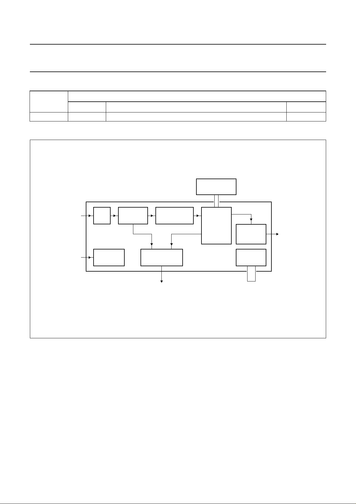
BLOCK DIAGRAM
handbook, full pagewidth
clock input
ADCHF input
CLOCK
GENERATOR
PLL BIT
DETECTOR
DEMODULATOR
EFM/EFM+
SPINDLE
MOTOR CONTROL
SRAM
32 KBYTES
DECODER
SAA7335
I2S-BUS
OUTPUT
INTERFACE
SUB-CPU
INTERFACE
block
decoder
output
motor control
Fig.1 Simplified block diagram.
MGK242
2001 apr 05 3
Page 4

Philips Semiconductors Preliminary specification
DSP for CD and DVD-ROM systems SAA7335
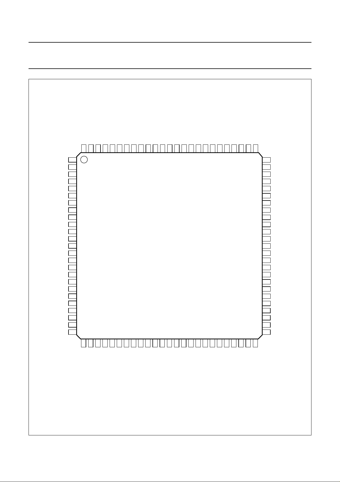
PINNING
SYMBOL PIN TYPE DESCRIPTION
V
SSA1
I
ref
REFLo 3 I analog low reference input for ADC
REFHi 4 I analog high reference input for ADC
VREF 5 I analog negative input
HFIN 6 I analog positive input
V
SSA2
AGCOUT 8 O analog test pin output
V
DDA2
V
DDD1
V
SSD1
OTD 12 I off track detect input
MOTO1 13 O 3-state motor control output
n.c. 14 − not connected, reserved
MOTO2/T3 15 I/O motor control output/tachometer 3 input
n.c. 16 − not connected, reserved
T1 17 I tachometer 1 input
T2 18 I tachometer 2 input
V
DDD2
V
SSD2
TEST1 21 I test input 1
TEST2 22 I test input 2
POR 23 I power-on reset input
MUXSWICH 24 I use clock multiplier input
n.c. 25 − not connected, reserved
CL1 26 O divided clock output
BCAIN 27 I BCA input
SDA 28 I/O sub-CPU I
SCL 29 I sub-CPU I
INT 30 O sub-CPU interrupt output (open-drain)
V
DDD3
V
SSD3
da7 33 I/O sub-CPU data bus bit 7 input/output (parallel)
da6 34 I/O sub-CPU data bus bit 6 input/output (parallel)
da5 35 I/O sub-CPU data bus bit 5 input/output (parallel)
n.c. 36 − not connected, reserved
da4 37 I/O sub-CPU data bus bit 4 input/output (parallel)
n.c. 38 − not connected, reserved
da3 39 I/O sub-CPU data bus bit 3 input/output (parallel)
da2 40 I/O sub-CPU data bus bit 2 input/output (parallel)
1 supply analog ground 1
2 I analog current reference input for ADC
7 supply analog ground 2
9 supply analog supply voltage 2
10 supply digital supply voltage 1
11 supply digital ground 1
19 supply digital supply voltage 2
20 supply digital ground 2
2
C-bus serial data input/output
2
C-bus serial clock input
31 supply digital supply voltage 3
32 supply digital ground 3
2001 apr 05 4
Page 5

Philips Semiconductors Preliminary specification
DSP for CD and DVD-ROM systems SAA7335
SYMBOL PIN TYPE DESCRIPTION
da1 41 I/O sub-CPU data bus bit 1 input/output (parallel)
n.c. 42 − not connected, reserved
da0 43 I/O sub-CPU data bus bit 0 input/output (parallel)
V
DDD4
V
SSD4
WRi 46 I sub-CPU write enable input (active LOW)
RDi 47 I sub-CPU read enable input (active LOW)
ALE 48 I sub-CPU address latch enable input
CSi 49 I sub-CPU chip select input (active HIGH)
STOPCLOCK 50 O stop clock output
n.c. 51 − not connected, reserved
V4 52 O serial subcode output (for CD)
EBUOUT 53 O digital audio output
SYNC 54 O I
FLAG 55 O I
DATA 56 O I
BCLK 57 I/O I
WCLK 58 I/O I
V
DDD5
V
SSD5
RAMRW 61 O RAM read/write control output
n.c. 62 − not connected, reserved
RAMDA7 63 I/O RAM data bus bit 7 input/output
RAMDA6 64 I/O RAM data bus bit 6 input/output
RAMDA5 65 I/O RAM data bus bit 5 input/output
RAMDA4 66 I/O RAM data bus bit 4 input/output
RAMDA3 67 I/O RAM data bus bit 3 input/output
RAMDA2 68 I/O RAM data bus bit 2 input/output
n.c. 69 − not connected, reserved
RAMDA1 70 I/O RAM data bus bit 1 input/output
RAMDA0 71 I/O RAM data bus bit 0 input/output
V
DDD6
V
SSD6
RAMAD0 74 O RAM address bit 0 output
RAMAD1 75 O RAM address bit 1 output
RAMAD2 76 O RAM address bit 2 output
RAMAD3 77 O RAM address bit 3 output
RAMAD4 78 O RAM address bit 4 output
RAMAD5 79 O RAM address bit 5 output
RAMAD6 80 O RAM address bit 6 output
V
DDD7
44 supply digital supply voltage 4
45 supply digital ground 4
2
S-bus sector sync output
2
S-bus correction flag output
2
S-bus serial data output
2
S-bus bit serial clock input/output
2
S-bus word clock input/output
59 supply digital supply voltage 5
60 supply digital ground 5
72 supply digital supply voltage 6
73 supply digital ground 6
81 supply digital supply voltage 7
2001 apr 05 5
Page 6

Philips Semiconductors Preliminary specification
DSP for CD and DVD-ROM systems SAA7335
SYMBOL PIN TYPE DESCRIPTION
V
SSD7
RAMAD7 83 O RAM address bit 7 output
RAMAD8 84 O RAM address bit 8 output
RAMAD9 85 O RAM address bit 9 output
n.c. 86 − not connected, reserved
RAMAD10 87 O RAM address bit 10 output
RAMAD11 88 O RAM address bit 11 output
RAMAD12 89 O RAM address bit 12 output
RAMAD13 90 O RAM address bit 13 output
RAMAD14 91 O RAM address bit 14 output
V
DDD8
V
SSD8
CRIN 94 I analog crystal input
CROUT 95 O analog crystal output
CFLG 96 O correction statistics output
MEAS1 97 O front-end telemetry output
V
DDD9
V
SSD9
V
DDA1
82 supply digital ground 7
92 supply digital supply voltage 8
93 supply digital ground 8
98 supply digital supply voltage 9
99 supply digital ground 9
100 supply analog supply voltage 1
2001 apr 05 6
Page 7
Philips Semiconductors Preliminary specification
DSP for CD and DVD-ROM systems SAA7335
handbook, full pagewidth
V
SSA1
I
ref
REFLo
REFHi
VREF
HFIN
V
SSA2
AGCOUT
V
DDA2
V
DDD1
V
SSD1
OTD
MOTO1
n.c.
MOTO2/T3
n.c.
T1
T2
V
DDD2
V
SSD2
TEST1
TEST2
POR
MUXSWICH
n.c.
1
2
3
4
5
6
7
8
9
10
11
12
13
14
15
16
17
18
19
20
21
22
23
24
25
DDA1VSSD9VDDD9
V
100
MEAS1
CFLG
99989796959493929190898887868584838281
CROUT
CRIN
SSD8VDDD8
V
RAMAD14
RAMAD13
RAMAD12
RAMAD11
RAMAD10
n.c.
RAMAD9
RAMAD8
SAA7335
SSD7VDDD7
RAMAD7
V
RAMAD6
RAMAD5
RAMAD4
RAMAD3
8079787776
RAMAD2
75
74
73
72
71
70
69
68
67
66
65
64
63
62
61
60
59
58
57
56
55
54
53
52
51
RAMAD1
RAMAD0
V
SSD6
V
DDD6
RAMDA0
RAMDA1
n.c.
RAMDA2
RAMDA3
RAMDA4
RAMDA5
RAMDA6
RAMDA7
n.c.
RAMRW
V
SSD5
V
DDD5
WCLK
BCLK
DATA
FLAG
SYNC
EBUOUT
V4
n.c.
26
CL1
SDA
BCAIN
31323334353637383940414243444546474849
SCL
INT
DDD3
V
SSD3
V
da7
da6
da5
n.c.
da4
30
29
28
27
Fig.2 Pin configuration.
2001 apr 05 7
n.c.
da3
da2
da1
n.c.
da0
DDD4
V
SSD4
V
WRi
RDi
ALE
50
CSi
STOPCLOCK
MGK241
Page 8

Philips Semiconductors Preliminary specification
DSP for CD and DVD-ROM systems SAA7335
FUNCTIONAL DESCRIPTION
Analog front-end
ThisblockconvertstheHFinputtothe digital domain using
an 8-bit ADC proceeded by an AGC circuit to obtain the
optimum performance from the convertor. This block is
clocked by ADCCLK which is set by the external crystal
frequency plus a flexible clock multiplier and divider block.
PLL and bit detector
This subsystem recovers the data from the channel
stream. The block corrects asymmetry, performs noise
filtering and equalisation and finally recovers the bit clock
and data from the channel using a digital PLL.
The equalizer and the data slicer are programmable.
Digital logic
All the digital system logic is clocked from the master ADC
clock (ADCCLK) described above.
Advanced bit detector
The advanced bit detector offers improved data recovery
for multi-layer discs and contains two extra detection
circuits to increase the margins in the bit recovery block:
1. Adaptive slicer: adds a second stage slicer with higher
bandwidth
2. Runlength 2 push-back: all T2 runlengths are pushed
back to T3, thereby automatically determining the
erroneous edge and shifting the transitions on that
edge.
Demodulator
FRAME SYNC PROTECTION CD MODE
This circuit detects the frame synchronization signals.
Two synchronization counters are used in the SAA7335:
1. The coincidence counter: this is used to detect the
coincidence of successive syncs. It generates a sync
coincidence signal if 2 syncs are 588 ±1 EFM clocks
apart.
2. The main counter: this is used to partition the EFM
signal into 17-bit words. This counter is reset when:
a) A sync coincidence is generated
b) A sync is found within ±6 EFM clocks of its
expected position.
The sync coincidence signal is also used to generate the
lock signal which will go active HIGH when 1 sync
coincidence is found. It will reset to LOW when, during
61 consecutive frames, no sync coincidence is found.
FRAME SYNC PROTECTION DVD MODE
This circuit detects the frame synchronization signals.
Two synchronization counters are used in the SAA7335:
1. The coincidence counter: this is used to detect the
coincidence of successive syncs. It generates a sync
coincidence signal if 2 syncs are 1488 ±3 EFM+
clocks apart.
2. The main counter: this is used to partition the EFM+
signal into 16-bit words. This counter is reset when:
a) A sync coincidence is generated
b) A sync is found within ±10 EFM+ clocks of its
expected position.
The sync coincidence signal is also used to generate the
lock signal which will go active HIGH when 1 sync
coincidence is found. It will reset to LOW when, during
61 consecutive frames, no sync coincidence is found.
EFM/EFM+ demodulation
The 14-bit EFM (16-bit EFM+) data and subcode words
are decoded into 8-bit symbols.
2001 apr 05 8
Page 9

Philips Semiconductors Preliminary specification
DSP for CD and DVD-ROM systems SAA7335
Microcontroller interface
The SAA7335 has two microcontroller interfaces, one
serial I2C-bus and one parallel (8051 microcontroller
compatible).
The two communication modes may be operated at the
same time, the modes are described below:
1. Parallel mode: protocol compatible with 8052
multiplexed bus:
a) da0 to da7 = address/data bus
b) ALE = Address Latch Enable, latches the address
information on the bus
c) WRi = active LOW write signal for write to
SAA7335
d) RDi = active LOW read signal for read from
SAA7335
e) CSi = active HIGH Chip Select signal (this signal
gates the RDi and WRi signals).
2. I2C-bus mode: I2C-bus protocol where SAA7335
behaves as slave device where:
a) SDA = I2C-bus data
b) SCL = I2C-bus clock
c) I2C-bus slave address (write mode) = 3EH
d) I2C-bus slave address (read mode) = 3FH
e) Maximum data transfer rate = 400 kbits/s.
ICROCONTROLLER INTERFACE (I
M
2
C-BUS MODE)
Thesequenceforawritedatacommand(1 data byte) is as
follows:
• Send START condition
• Send address 3EH (write)
• Write command address byte
• Write data byte
• Send STOP condition.
Thesequence for a read data command(that reads 1 data
byte) is as follows:
• Send START condition
• Send address 3EH (write)
• Write status address byte
• Send STOP condition
• Send START condition
• Send address 3FH (read)
• Read data byte
• Send STOP condition.
R
EADING AND WRITING DATA TO THE SAA7335
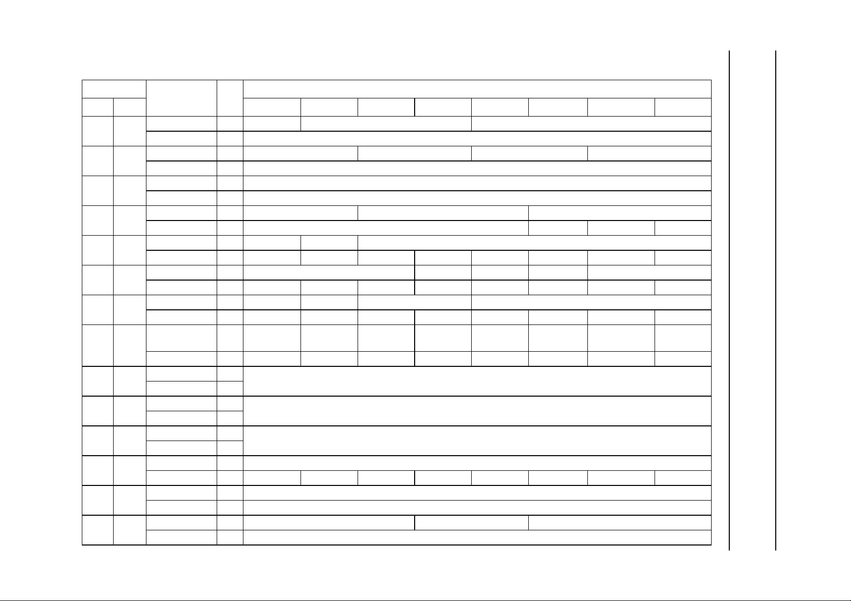
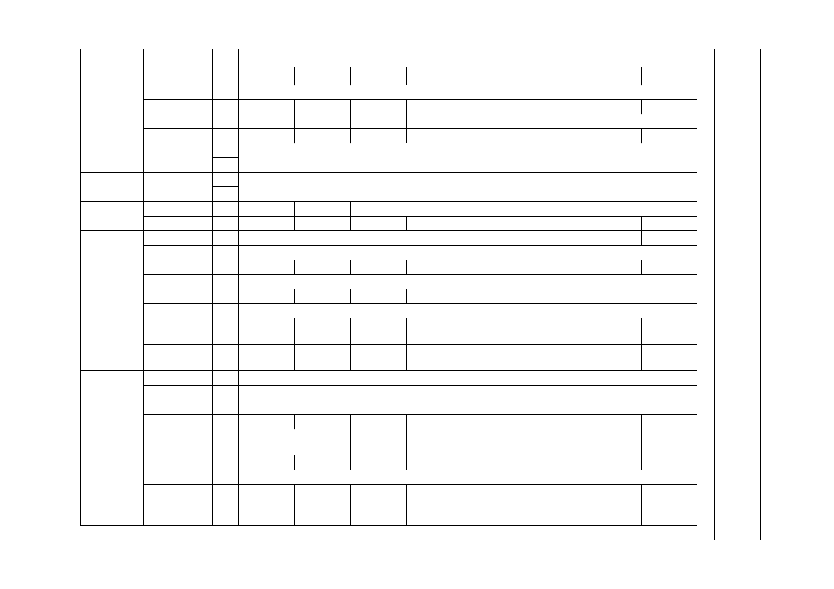
The SAA7335 has 32 × 8-bit configuration and status
registers as shown in Table 1. Not all locations are
currently defined and some remain reserved for future
upgrades. These can be written to or read from via the
microcontroller interface using either the serial or parallel
control bus.
Bytes are transferred over the interface in single bytes of
which there are two types; write data commands and read
data commands.
2001 apr 05 9
Page 10
This text is here in white to force landscape pages to be rotated correctly when browsing through the pdf in the Acrobat reader.This text is here in
_white to force landscape pages to be rotated correctly when browsing through the pdf in the Acrobat reader.This text is here inThis text is here in
white to force landscape pages to be rotated correctly when browsing through the pdf in the Acrobat reader. white to force landscape pages to be ...
2001 apr 05 10
REGISTER MAP
Table 1 SAA7335 microcontroller register map
ADDRESS
DEC HEX 7 6 5 4 3 2 1 0
0 0 PLL_LOCK W Lock Oride Pha_Oset PLL_Force_L
1 1 PLL_SET W SliceBW Integ_F0 PLLBW_F1 LP_BW_F3
2 2 PLL_FREQ W PLL frequency (8 MSBs)
3 3 PLL_EQU W PLL frequency (2 LSBs) equalizer tap α 1 equaliser tap α 2
4 4 PLL_F_MEAS W RL3_EN reserved EFM nominal setting (101110)
5 5 OUTPUT1 W Fmat(3 to 1) WCLK_Op BCLK_Op Fmat (0) SyncSwap (1 and 0)
6 6 OUTPUT2 W EBU_Valid EBU_On EBU control bits 28, 29 EBU control bits (1 to 4)
7 7 OUTPUT3 W WCLK_H_
8 8 SEMA1 W general purpose semaphore register
9 9 SEMA2 W general purpose semaphore register
10 A SEMA3 W general purpose semaphore register
11 B INTEN W hardware pin interrupt enable bits (map to status bits)
12 C MOTOR1 W frequency set point
13 D MOTOR2 W G(2 to 0) Ki Kf
NAME R/W
PLL_Freq_R R PLL measured frequency (bits 9 to 2)
PLL_ASSYM R PLL asymmetry value (8 bits)
PLL_Jit R jitter value (bits 9 to 2)
PLL_Lock_In R reserved Long_Symb F_Lock In_Lock
reserved R −−−−−− − −
reserved R −−−−−− − −
reserved R −−−−−− − −
Descr_On Interp_On CD_ROM_
Left
reserved R −−−−−− − −
R
R
R
Status R Fl_S1 Fl_S2 Fl_S3 PLL lock DVD rdy Mot Ov Tacho reserved
SLICE1 R slice compensation value
EYE_Open R eye opening value
Header_On
BIT
Flag_Pin Kill Data On Kill EBU_On CD_ROM_
Philips Semiconductors Preliminary specification
DSP for CD and DVD-ROM systems SAA7335
Scrb_On
Page 11
This text is here in white to force landscape pages to be rotated correctly when browsing through the pdf in the Acrobat reader.This text is here in
_white to force landscape pages to be rotated correctly when browsing through the pdf in the Acrobat reader.This text is here inThis text is here in
white to force landscape pages to be rotated correctly when browsing through the pdf in the Acrobat reader. white to force landscape pages to be ...
2001 apr 05 11
ADDRESS
DEC HEX 7 6 5 4 3 2 1 0
14 E MOTOR3 W FIFO set point
15 F MOTO4 W PWM_PDM OVF_SW SW2 SW1 motor servo control (3 to 0)
16 10 MTR_INTG_L W motor integrator value (7 to 0)
17 11 MTR_INTG_H W motor integrator value (15 to 8)
18 12 CLOCKPRE W CL1Div BCLKG_En Div1 (2 to 0) Mux 2 Div2 (2 to 0)
19 13 DECMODE W mode reserved read TOC reserved
20 14 reserved W −−−−−− − −
21 15 ANASET W AGC_En gain set gain up gain down AGC_On reserved
22 16 VITSET W slice ON AdDet ON FEndAutoS
23 17 TACHO1 W tachometer multiplier frequency KTacho (7 to 0)
24 18 TACHO2 W tachometer interrupt trip frequency tachometer trip (7 to 0)
25 19 TACHO3 W servo control source Tacho
26 1A BCASET W BCA_Freq (7 to 0)
27 to311B to
1F
NAME R/W
MTR_F R −−−−−− − −
reserved R −−−−−− − −
R
R
SUB_C_STAT R ready busy CRC_OK err (2 to 0) cor fail reserved
SUB_C_DATA R subcode data (7 to 0)
SUB_C_End R no meaning (register read used as a signal)
FIFOFILL_L R number of C1 frames in FIFO
ON
BCA_STAT R Buff_
Loaded
BCA_DATA R BCA data (7 to 0)
reserved R −−−−−− − −
reserved R −−−−−− − −
reserved R −−−−−− − −
reserved −−−−−− − −
sync Buff_ORun
Moto2_T3 Fsam TachoInt_LF reserved
FRes
BIT
Philips Semiconductors Preliminary specification
DSP for CD and DVD-ROM systems SAA7335
Page 12

Philips Semiconductors Preliminary specification
DSP for CD and DVD-ROM systems SAA7335
READING STATUS INFORMATION FROM THE SAA7335
There are several internal status signals which can be made available on the INT line (see Table 2).
Table 2 Internal status signals; note 1
SIGNAL DESCRIPTION
Fl_S1 change in semaphore register 1 detected
Fl_S2 change in semaphore register 2 detected
Fl_S3 change in semaphore register 3 detected
PLLlock channel data PLL lock (not latched) indicates in-lock condition
DVDrdy DVD header or subcode block is available, reset when SUBREADEND register is read
MotOv motor overflow, (not latched) indicates when a motor overflow is occurring
Tacho motor speed is higher (or lower depending on TACHO3 bit 2) than motor set point (defined in
TACHO2) this signal is not latched
Note
1. The status signal to be output is selected by interrupt control register.
Subcode data/DVD header processing
Q-CHANNEL PROCESSING
The 96-bit Q-channel word is accumulated in an internal
buffer. Sixteen bits are used to perform a Cyclic
Redundancy Check (CRC). Subcode is available via the
V4 outputand, in addition, the Q channelcode can also be
read via the SUBREADDATA register.
DVD HEADER
The DVD header processor accumulates a selection of
bytes from the beginning of the DVD sector. Two header
modes are defined, one for reading the normal sector
headers and one for filtering the disk physical format
information(fromthe control data block in the lead-in area)
This is controlled by the READ_TOC bit in the DECMODE
register.
OTHER SUBCODE CHANNELS
Data of the other subcode channels (Q-to-W) may be read
via the V4 pin, this is only valid in CD modes.
Thedata on the V4 pin is clocked on theWCLK edges with
a fixed delay and so may be clocked by external circuitry
running off the WCLK edges, i.e. at twice the WCLK
frequency.The subcode data is also available in the EBU
output (DOBM) in a similar format.
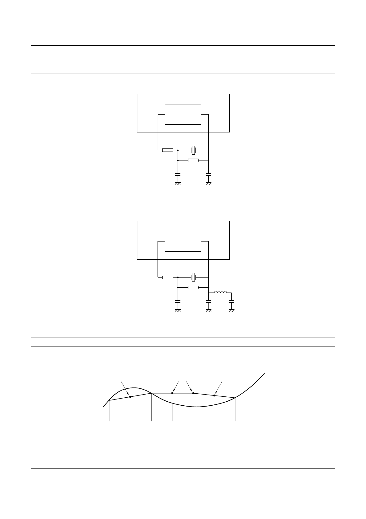
and with both fundamental and third overtone crystals.
External components should be used to suppress the
fundamentaloutputof the third overtone crystals as shown
in Figs 3 and 4. Typical oscillation frequencies required
are 8.462, 16.9344 or 22.57 MHz depending on the
internal clock settings used and whether or not the clock
multiplier is enabled.
Error corrector
The error corrector can operate in a number of modes; CD
single-pass, CD dual-pass and DVD mode. In the CD
single-pass mode the error corrector performs 2 error
corrections per frame (C1 and C2). In the CD dual-pass
mode up to 4 symbol corrections per frame are possible
(C1-C2 then C1-C2 again). For the DVD mode full depth
PI and PO error correction is performed allowing
5 corrections per PI row and full depth (2t + e)
≤16 correction to be performed per PO column. The error
corrector also contains a flag controller. Flags are
assigned to symbols when the error corrector cannot
ascertain if the symbols are definitely good. C1 generates
output flags which are read (after de-interleaving) by C2,
to help in the generation of C2 output flags. The C2 output
flags are used by the interpolator for concealment of
non-correctable errors. They are also output via the EBU
signal (DOBM) and the MISC output via the I2S-bus for
CD-ROM applications.
Crystal oscillator
The crystal oscillator is a conventional 2 pin design. This
oscillator is capable of operating with ceramic resonators
2001 apr 05 12
The flags output pin CFLG provides information on the
state of all error correction and concealment flags.
Page 13
Philips Semiconductors Preliminary specification
DSP for CD and DVD-ROM systems SAA7335
handbook, halfpage
SAA7335
OSCILLATOR
330 Ω
8.4672 MHz
100 kΩ
22
22
pF
pF
Fig.3 8.4672 MHz fundamental configuration.
handbook, halfpage
SAA7335
OSCILLATOR
22.57 MHz
CRINCROUT
MGK243
CRINCROUT
330 Ω
100 kΩ
10
pF
10
pF
3.3 µH
1 nF
MGK244
Fig.4 22.57 MHz overtone configuration.
Interpolation Hold Interpolation
OK Error OK Error Error Error OK OK
Fig.5 Concealment mechanism.
MGA372
2001 apr 05 13
Page 14
Philips Semiconductors Preliminary specification
DSP for CD and DVD-ROM systems SAA7335
Audio functions
CONCEALMENT
A 1-sample linear interpolator becomes active if a single
sample is flagged as erroneous but cannot be corrected.
The erroneous sample is replaced by a level midway
between the preceding and following samples. Left and
right channels have independent interpolators.
If more than one consecutive non-correctable sample is
found the last good sample is held. A 1-sample linear
interpolation is then performed before the next good
sample (see Fig.5).
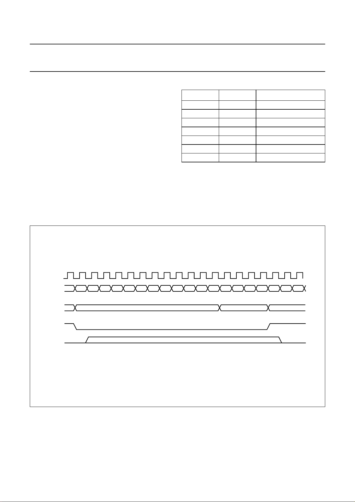
DAC Interface
The SAA7335 is compatible with a wide range of ROM
block decoders and Digital-to-Analog Converters DACs.
The seven main formats that are supported are given in
Table 3.
Table 3 DAC interface formats (notes 1, 2 and 3)
MODE BITS/WORD FORMAT
1 16 Philips I
2
S-bus
2 16 EIAJ
3 24 Philips I
2
S-bus
4 24 EIAJ
5 32 Philips I
2
S-bus
6 32 EIAJ
2
7 variable Philips I
S-bus
Notes
1. EIAJ is the abbreviation for Electronic Industries
Associated of Japan.
2. Number of BCLK periods per half WCLK period
(i.e. bits per sample).
3. Clock gating must be DISABLED for format mode 7.
handbook, full pagewidth
BCLK
DATA
MISC
WCLK
SYNC
D0 D15 D14 D13 D12 D11 D10 D9 D8 D7 D6 D5 D4 D3 D2 D1 D0 D15 D14
flag-MSB (1 is unreliable) flag-LSB flag-MSB
left
right
MGK245
Fig.6 Philips I2S-bus data format 1 (16-bit word length).
2001 apr 05 14
Page 15
Philips Semiconductors Preliminary specification
DSP for CD and DVD-ROM systems SAA7335
handbook, full pagewidth
handbook, full pagewidth
BCLK
DATA
MISC
WCLK
SYNC
BCLK
DATA
MISC
WCLK
SYNC
D0 D15 D14 D13 D12 D11 D10 D9 D8 D7 D6 D5 D4 D3 D2 D1 D0 D15 D14
flag-MSB (1 is unreliable) flag-LSB flag-MSB
right
left
MGK246
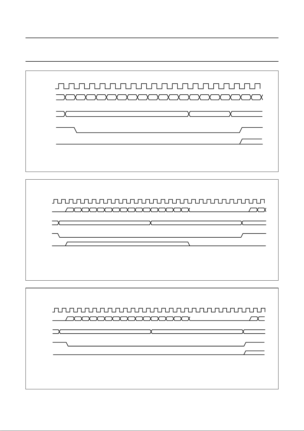
Fig.7 EIAJ (‘S’) data format 2 (16-bit word length).
D15 D14 D13 D12 D11 D10 D9 D8 D7 D6 D5 D4 D3 D2 D1 D0 D15 D14
flag-MSB (1 is unreliable) flag-LSB flag-MSB
left
right
MGK247
Fig.8 Philips I2S-bus data format 3 (24-bit word length).
BCLK
handbook, full pagewidth
DATA
MISC
WCLK
SYNC
D15 D14 D13 D12 D11 D10 D9 D8 D7 D6 D5 D4 D3 D2 D1 D0
flag-MSB (1 is unreliable)
right
Fig.9 EIAJ (‘S’) data format 4 (24-bit word length).
2001 apr 05 15
D15 D14
flag-LSB flag-MSB
left
MGK248
Page 16
This text is here in white to force landscape pages to be rotated correctly when browsing through the pdf in the Acrobat reader.This text is here in
_white to force landscape pages to be rotated correctly when browsing through the pdf in the Acrobat reader.This text is here inThis text is here in
white to force landscape pages to be rotated correctly when browsing through the pdf in the Acrobat reader. white to force landscape pages to be ...
2001 apr 05 16
BCLK
DATA
MISC
WCLK
SYNC
D15 D14 D13 D12 D11 D10 D9 D8 D7 D6 D5 D4 D3 D2 D1 D0 D15 D14
flag-MSB (1 is unreliable) flag-LSB flag-MSB
left
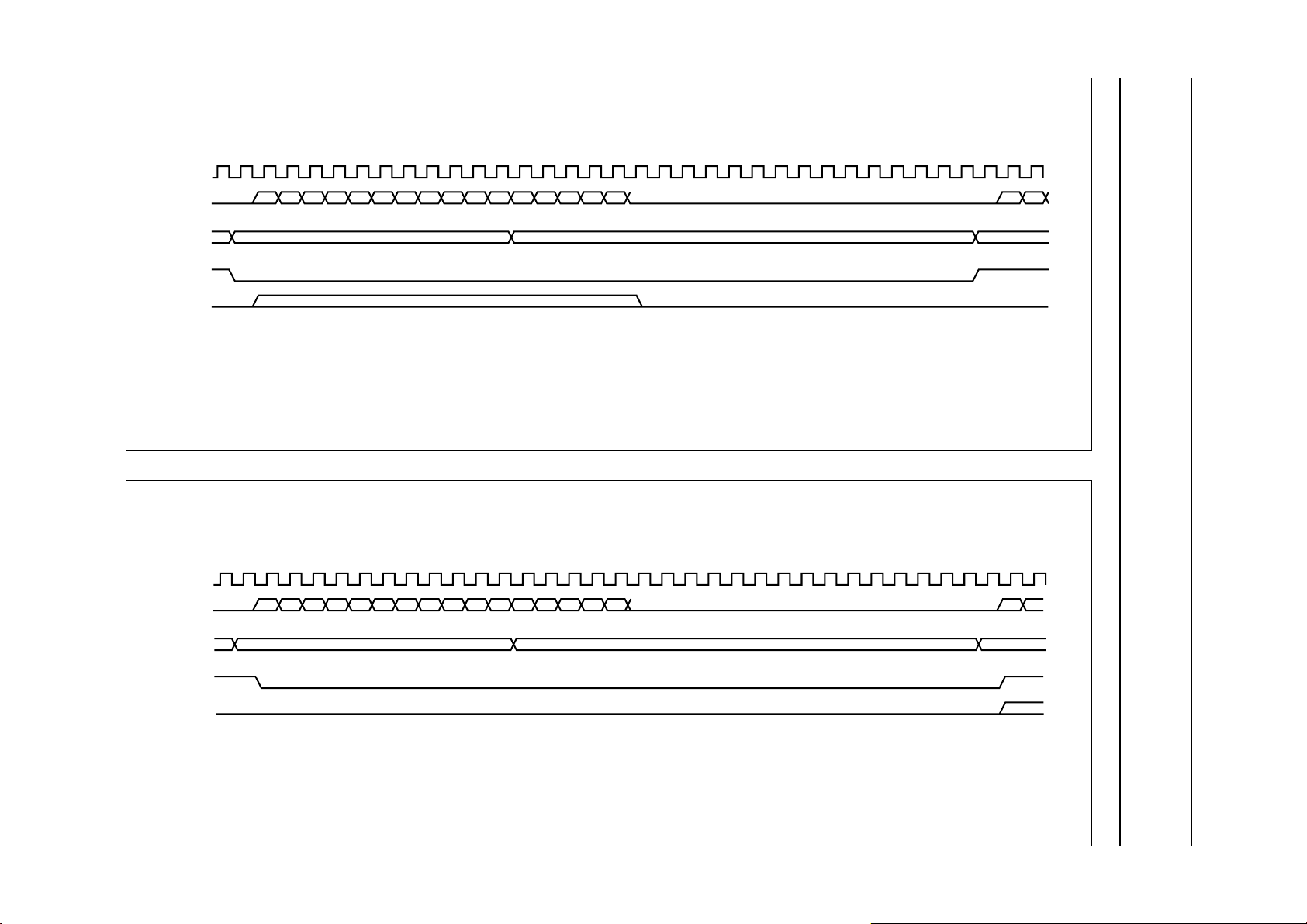
Fig.10 Philips I2S-bus data format 5 (32-bit word length).
Philips Semiconductors Preliminary specification
DSP for CD and DVD-ROM systems SAA7335
right
MGK249
BCLK
DATA
MISC
WCLK
SYNC
D15 D14 D15 D14D13 D12 D11 D10 D9 D8 D7 D6 D5 D4 D3 D2 D1 D0
flag-MSB (1 is unreliable) flag-LSB flag-MSB
right
left
MGK250
Fig.11 EIAJ (‘S’) data format 6 (24-bit word length).
Page 17
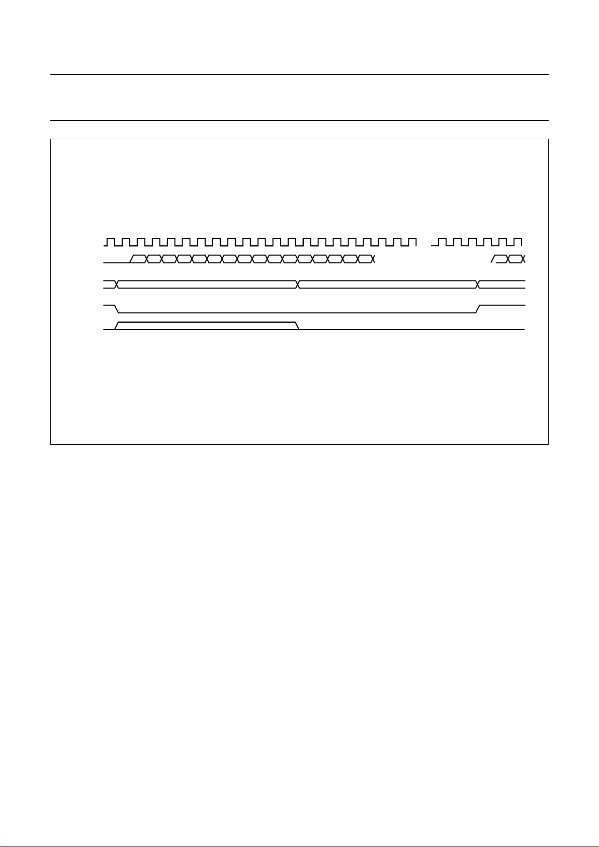
Philips Semiconductors Preliminary specification
DSP for CD and DVD-ROM systems SAA7335
handbook, full pagewidth
BCLK
DATA
FLAG
WCLK
SYNC
D15 D14 D13 D12 D11 D10 D9 D8 D7 D6 D5 D4 D3 D2 D1 D0
flag-MSB (1 is unreliable) flag-LSB
left
Fig.12 Philips I2S-bus data format (variable word length).
EBU interface
The biphase-mark digital output signal at pin DOBM is in
accordance with the format defined by the
“IEC 958”
specification.
variable number of clocks
D15 D14
flag-MSB
right
MGK251
AUDIO SAMPLE
Left and right samples are transmitted alternately.
VALIDITY FLAG
Three different modes can be selected via the EBU output
control register (address 1010).
FORMAT
The digital audio output consists of 32-bit words
(subframes) transmitted in biphase-mark code
(2 transitions for a logic 1 and one transition for a logic 0).
Words are transmitted in blocks of 384 (see Table 4).
SYNC
The sync word is formed by violation of the biphase rule
and therefore does not contain any data. Its length is
equivalent to 4 data bits. The three different sync patterns
indicate the following situations:
• Sync B: start of a block (384 words), word contains left
sample
• Sync M: word contains left sample (no block start)
• Sync W: word contains right sample.
2001 apr 05 17
Audio samples are flagged (bit 28 = logic 1) if an error has
been detected but was non-correctable. This flag remains
the same even if data is taken after concealment.
USER DATA
Subcode bits Q-to-W from the subcode section are
transmittedviatheuserdatabit. This data is asynchronous
with the block rate.
CHANNEL STATUS
The channel status bit is the same for left and right words.
Therefore a block of 384 words contains 192 channel
status bits. The category code is always CD. The bit
assignment is given in Table 5.
Page 18

Philips Semiconductors Preliminary specification
DSP for CD and DVD-ROM systems SAA7335
Table 4 EBU word format
WORD BITS FUNCTION
Sync 0 to 3 −
Auxiliary 4 to 7 not used; normally zero
Error flags 4 CFLG error and interpolation flags when bit 3 of EBU control register is set
to logic 1
Audio sample 8 to 27 first 4 bits not used (always zero)
Validity flag 28 valid = logic 0
User data 29 used for subcode data (Q-to-W)
Channel status 30 control bits and category code
Parity bit 31 even parity for bits 4 to 30
Table 5 EBU channel status
WORD BITS FUNCTION
Consumer/professional 0 always zero
Control 1 to 4 copied from bits 3 to 0 of register OUTPUT2, normally should be set to a
copy of CRC checked Q-channel control bits 0to 3; bit 2 is logic 1 when
copy permitted; bit 3 is logic 1 when recording has pre-emphasis
Reserved 5 to 7 always zero
Category code 8 to 15 CD; bit 8 = logic 1, all other bits = logic 0
Reserved 16 to 27 always zero
Clock accuracy 28 to 29 set by OUTPUT2 control register bits 5 and 4; 00 = level II, 01 = level III
Remaining 30 to 191 always zero
Spindle motor control
The spindle motor speed is controlled by a fully integrated
digital servo. Address information from the internal
±8 frame FIFO and disc speed information are used to
calculate the motor control output signals.
Several output modes are supported:
1. Pulse density, 1-line,
2. Pulsedensity,2-line(truecomplement output) (cannot
be used with tachometer control)
3. PWM output, 2-line.
Themodes are selected via the motor outputconfiguration
register.
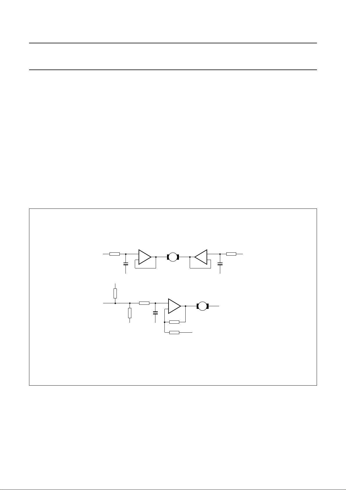
PULSE DENSITY MODE
In the pulse density mode the motor output (pin MOTO1)
is the pulse density modulated motor output signal. A 50%
2001 apr 05 18
dutycyclecorresponds with the motor not actuated, higher
duty cycles mean acceleration, lower mean braking.
In this mode, the MOTO2 signal is the inverse of the
MOTO1 signal. Both signals change state only on the
edges of a internal clock signal.
Possible application diagrams are shown in Fig.13.
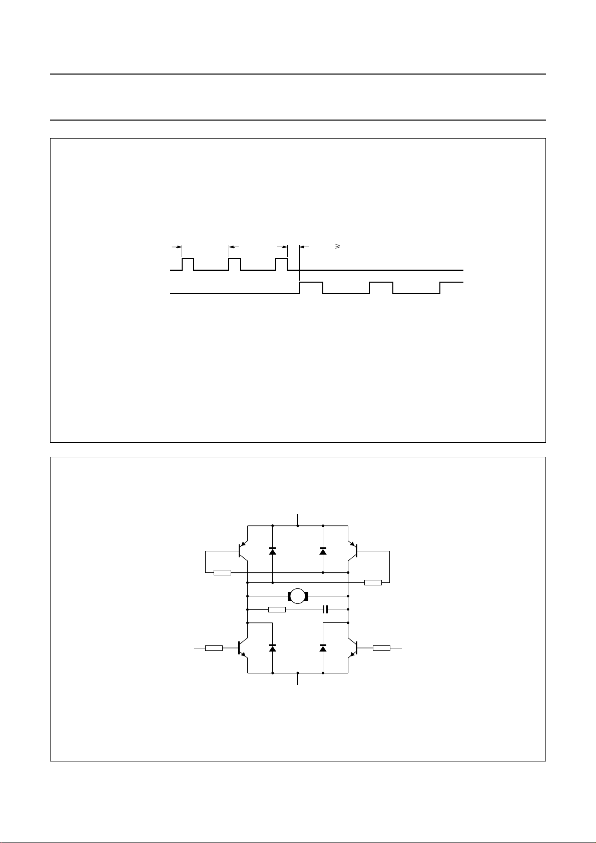
PWM MODE,2-LINE
In the PWM mode the motor acceleration signal is put in
pulse-width modulation form on the MOTO1 output and
the motor braking signal is pulse-width modulated on the
MOTO2 output.
Figure 14 illustrates the PWM mode timing and Fig.15
illustrates a typical PWM mode application diagram.
Page 19
Philips Semiconductors Preliminary specification
DSP for CD and DVD-ROM systems SAA7335
OPERATIONAL MODES
The motor servo has a number of operational modes controlled by the motor mode register MOTOR4.
POWER LIMIT
To start and stop the spindle motor, a fixed positive or negative voltage is applied to the motor. This voltage can be
programmed as a percentage of the maximum possible voltage via the motor output configuration register (MOTOR4) to
limit current drain during start and stop. The following power limits are possible:
• 100% of maximum (no power limit)
• 75% of maximum
• 50% of maximum
• 37% of maximum.
LOOP CHARACTERISTICS
The gain and crossover frequencies of the motor control loop can be programmed via the motor gain and bandwidth
register MOTOR2.
MOTO1
MOTO1
22 kΩ
22 kΩ
10 nF
V
DD
V
22 kΩ
SS
+
–
22 kΩ
M
+
SS
–
22 kΩ
22 kΩ
10 nF
V
SS
V
+
–
M
V
DD
Fig.13 Motor pulse density application diagrams.
V
SS
V
22 kΩ
10 nF
SS
MGA363 - 1
MOTO2
2001 apr 05 19
Page 20
Philips Semiconductors Preliminary specification
DSP for CD and DVD-ROM systems SAA7335
MOTO1
MOTO2
t = 45 µs
rep
t 240 ns
dead
Accelerate Brake
Fig.14 Motor 2-line PWM mode timing.
+
MGA366
10 Ω
MOTO1 MOTO2
V
Fig.15 Motor 2-line PWM mode application diagram.
2001 apr 05 20
M
SS
100 nF
MGA365 - 2
Page 21
Philips Semiconductors Preliminary specification
DSP for CD and DVD-ROM systems SAA7335
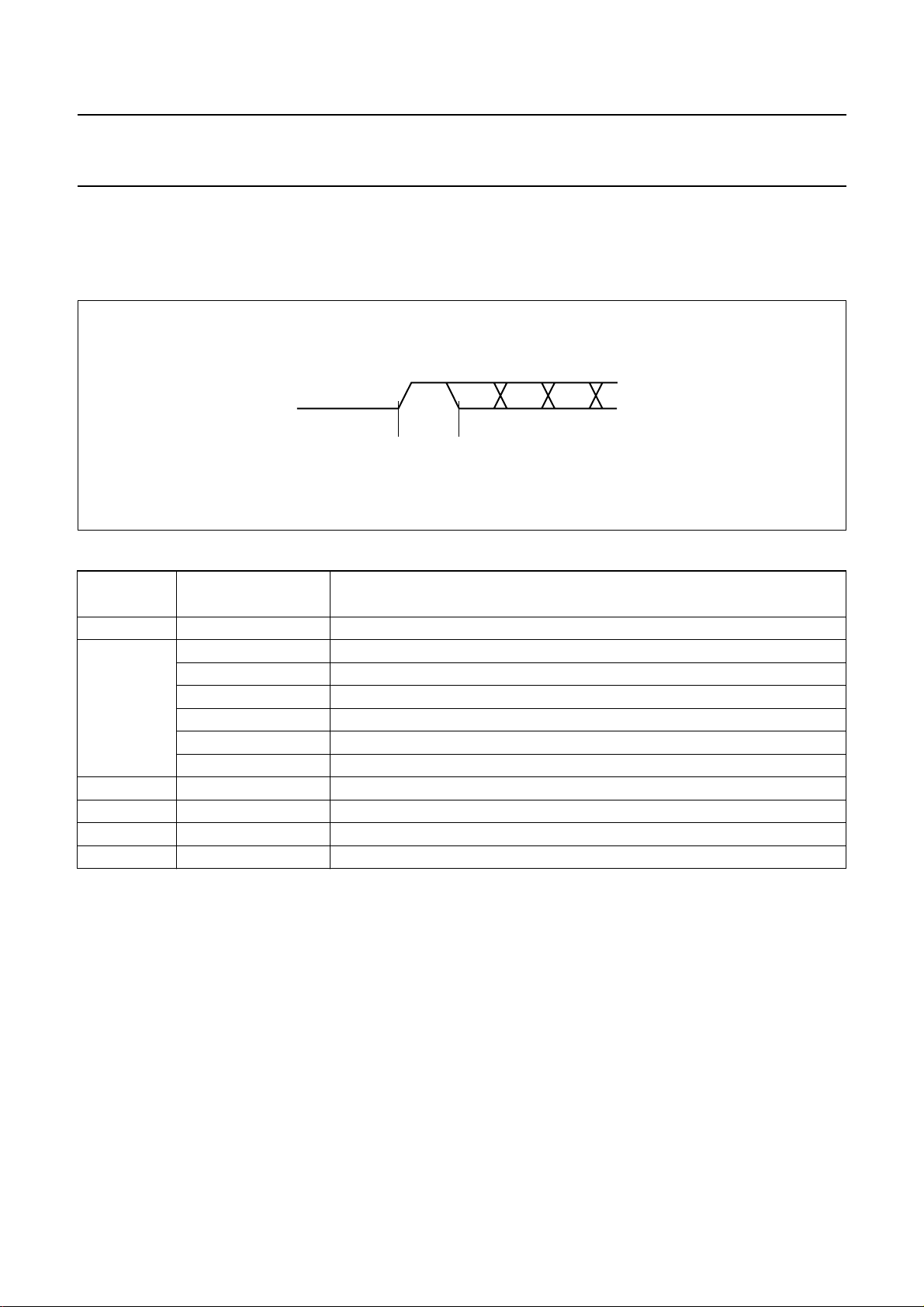
Flags output (CFLG) (open-drain output)
A1-bitflag signal is available at the CFLG pin, this contains 11 bits runningoffthe ADCCLK, each bit period is 7 ADCCLK
periods. This signal shows the status of the error corrector and interpolator and is updated every frame.
handbook, halfpage
START
bit
data bitspause
MGK252
Fig.16 Flags output format.
Table 6 Definition of flag bits
BIT
NUMBER
VALUE DESCRIPTION
0 1 START bit
1 to 3 000 C1 first or C1 last; note 1
001 C2 first, CD mode reserved, DVD mode; note 1
010 reserved; note 1
011 C2 last; note 1
100 corrector not active; note 1
all others reserved
4 core fail failure flag set because correction impossible; note 2
5 flag fail; note 3
9, 6 to 8 root count (3 to 0) this indicates the number of errors corrected; note 4
10 0 STOP bit
Notes
1. For DVD mode read PI for C1 and PO for C2.
2. This flag refers to the previous correction frame.
3. This flag refers to the previous correction frame (is not valid i.e. always logic 0 in DVD mode).
4. Bit order of root count is 9, then 6 to 8 for root count (3 to 0).
A
BSOLUTE TIME SYNC
The sync signal is the absolute time sync signal. In the CD mode it is the FIFO-passed subcode sync and relates the
position of the subcode sync to the audio data (DAC output). In the DVD mode it indicates the start of a new sector
header.
The flag may be used for special purposes such as synchronization of different players.
2001 apr 05 21
Page 22

Philips Semiconductors Preliminary specification
DSP for CD and DVD-ROM systems SAA7335
LIMITING VALUES
In accordance with the Absolute Maximum Rating System (IEC 134).
SYMBOL PARAMETER CONDITIONS MIN. MAX. UNIT
V
DDD
V
DDA
V
i(max)
V
o(max)
I
o(max)
T
amb
T
stg
V
ESD
Notes
1. This maximum value has an absolute maximum of 6.5 V independent of the supply voltage.
2. The human body model ESD simulation is equivalent to discharging a 100 pF capacitor via a 1.5 kΩ resistor, which
produces a single discharge transient. Reference
to MIL-STD 883C method 3015.7)”
3. The machine model ESD simulation is equivalent to discharging a 200 pF capacitor via a resistor and series inductor
with effective dynamic values of 25 Ω and 2.5 µH, which produces a damped oscillating discharge. Reference
“Philips Semiconductors Test Method UZW-BO/FQ-B302 (similar to EIAJ IC-121 Test Method 20 condition C)”
digital supply voltage −0.3 +6.5 V
analog supply voltage −0.3 +6.5 V
maximum input voltage (any input) note 1 −0.3 VDD+ 0.5 V
maximum output voltage (any output) note 1 − VDD+ 0.5 V
maximum output current (each output) −±10 mA
operating ambient temperature −20 +70 °C
storage temperature −55 +125 °C
electrostatic handling
human body model note 2 −2000 +2000 V
machine model note 3 −200 +200 V
“Philips Semiconductors Test Method UZW-BO/FQ-A302 (similar
.
.
QUALITY
This device will meet the requirements of the
in accordance with
“Quality Reference Handbook (order number 9397 750 00192)”
for all Q & R tests applied to the product.
“Philips Semiconductors General Quality Specification UZW-BO/FQ-0601”
. This details the acceptance criteria
2001 apr 05 22
Page 23
Philips Semiconductors Preliminary specification
DSP for CD and DVD-ROM systems SAA7335
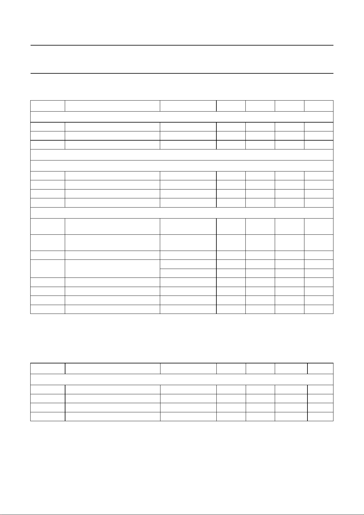
DC CHARACTERISTICS
V
DDD=VDDA
SYMBOL PARAMETER CONDITIONS MIN. TYP. MAX. UNIT
Supplies
V
DDD
V
DDA
I
DD(tot)
Inputs
DIGITAL INPUTS (TTL LEVEL); note 1
V
IL
V
IH
V
OL
V
OH
ANALOG INPUTS
V
I(max)(p-p)
V
I(nom)(p-p)
DR dynamic range 41 −−dB
B −3 dB bandwidth 0 to 12 dB gain −−−MHz
I
I(AGC)
I
I(ADC)
I
I(buf)
I
I(tot)
= 5 to 5.5 V; V
SSD=VSSA
=0V; T
= −20 to +70 °C; unless otherwise specified.
amb
digital supply voltage 4.5 − 5.5 V
analog supply voltage 4.5 − 5.5 V
total supply current at 25 MHz clock − 60 − mA
LOW-level input voltage −−0.8 V
HIGH-level input voltage 2.0 −−V
LOW-level output voltage 0.8 −−V
HIGH-level output voltage −−2.4 V
maximum input voltage
−−2V
(peak-to-peak value)
nominal input voltage
− 1 − V
(peak-to-peak value)
12 to 20 dB gain −−−MHz
AGC input current − 1 − mA
ADC input current − 24 − mA
output buffer input current − 3 − mA
total input current −−28 mA
Note
1. These inputs are analog, V
and VIH values are quoted as a guide for digital RGB users.
IL
AC CHARACTERISTICS
V
DDD=VDDA
= 4.5 to 5.5 V; V
SSD=VSSA
=0V; T
= −20 to +70 °C; unless otherwise specified.
amb
SYMBOL PARAMETER CONDITIONS MIN. TYP. MAX. UNIT
Supplies
V
I
DDD
V
I
DDA
DDD
DDA
digital supply voltage 4.5 5.0 5.5 V
digital supply current V
=5V − 60 165 mA
DDD
analog supply voltage 4.5 5.0 5.5 V
analog supply current V
=5V − 60 165 mA
DDA
2001 apr 05 23
Page 24
Philips Semiconductors Preliminary specification
DSP for CD and DVD-ROM systems SAA7335
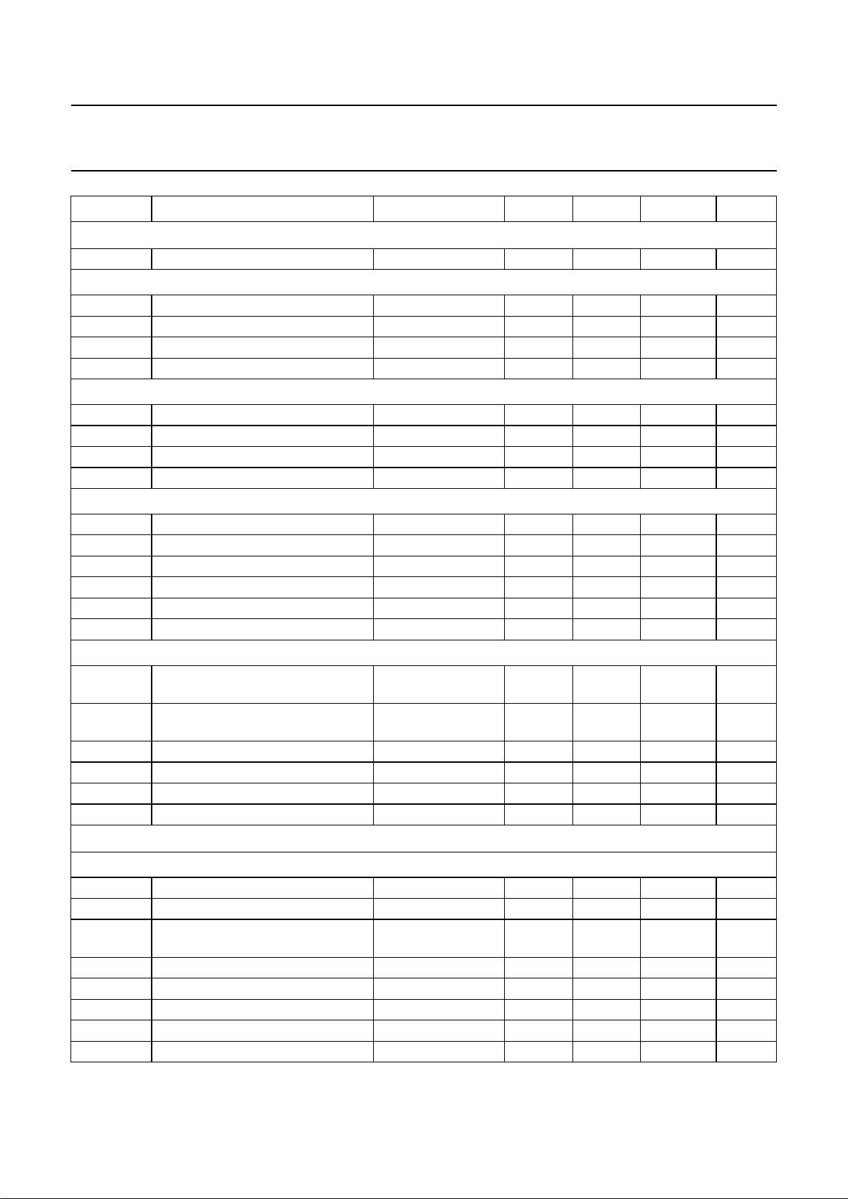
SYMBOL PARAMETER CONDITIONS MIN. TYP. MAX. UNIT
Analog front-end (V
f
chan
channel frequency −−50 MHz
= 4.5 to 5.5 V); HFIN
DDA
Digital inputs
V
IL
V
IH
I
LI
C
i
LOW-level input voltage −−0.8 V
HIGH-level input voltage 2.0 −− V
input leakage current Vi= 0 to V
input capacitance −−10 pF
Open-drain output; pin INT
V
OL
I
OL
C
L
t
o(f)
LOW-level output voltage IOL= 1 mA 0 − 0.4 V
LOW-level output current −−0mA
load capacitance −−50 pF
output fall time CL= 20 pF; note 1 −−15 ns
3-state outputs
V
OL
V
OH
C
L
t
o(r)
t
o(f)
I
LI(Z)
LOW-level output voltage IOL= 0 mA 0 − 0.4 V
HIGH-level output voltage IOH= −8 mA 2.4 −− V
load capacitance −−50 pF
output rise time CL= 20 pF; note 1 −−15 ns
output fall time CL= 20 pF; note 1 −−15 ns
3-state leakage current Vi= 0 to V
3-state outputs; pins MOTO1, MOTO2 and DOBM
V
OL
V
OH
C
L
t
o(r)
t
o(f)
I
LI(Z)
Digital input/outputs (V
NPUT/OUTPUT:SDA(INPUT/OPEN-DRAIN I
I
V
IL
V
IH
V
OL
I
OL
C
SDA
C
SCL
N
marL
N
marH
LOW-level output voltage V
HIGH-level output voltage V
load capacitance −−50 pF
output rise time CL= 20 pF; note 1 −−10 ns
output fall time CL= 20 pF; note 1 −−10 ns
3-state leakage current Vi= 0 to V
= 4.5 to 5.5 V)
DDD
2
C-BUS OUTPUT)
LOW-level input voltage −−1.5 V
HIGH-level input voltage 3.0 −− V
LOW-level output voltage IOL= 2 mA;
LOW-level output current −−− mA
serial data line capacitance −−10 pF
serial clock line capacitance −−10 pF
LOW-level noise margin − 0.1V
HIGH-level noise margin − 0.2V
DDD
DDD
= 4.5 to 5.5 V;
DDD
IOL=10mA
= 4.5 to 5.5 V;
DDD
IOH= −10 mA
DDD
I
=3mA
sink
−10 − +10 µA
−10 − +10 µA
0 − 0.8 V
−1 − +2.4 V
−10 − +10 µA
−−0.4 V
−
DDD
−
DDD
2001 apr 05 24
Page 25
Philips Semiconductors Preliminary specification
DSP for CD and DVD-ROM systems SAA7335
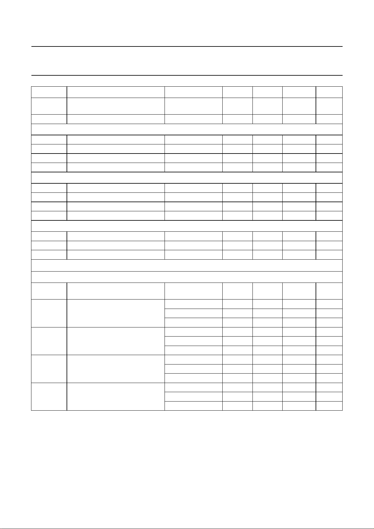
SYMBOL PARAMETER CONDITIONS MIN. TYP. MAX. UNIT
R
s
C
bus(max)
INPUT: SCL (CMOS INPUT)
V
IL
V
IH
I
LI
C
i
Crystal oscillator input CRIN (external clock)
g
m
R
o
C
i
I
LI
Crystal oscillator output CROUT (see Figs 3 and 4)
f
xtal
C
fb
C
o
2
S-bus timing
I
series resistance on the SDA and
− 300 −Ω
SCL lines
maximum bus capacitance per wire − 400 − pF
LOW-level input voltage −0.3 − 0.3V
HIGH-level input voltage 0.7V
input leakage current Vi=0−V
DDD
−10 − +10 µA
DDD
− V
DDD
DDD
V
+ 0.3 V
input capacitance −−10 pF
mutual conductance at start-up − 4 − mS
output resistance at start-up − 11 − kΩ
input capacitance −−10 pF
input leakage current −10 − +10 µA
crystal frequency 4 25 − MHz
feedback capacitance −−5pF
output capacitance −−10 pF
CLOCK OUTPUT SCLK (see Fig.17)
T
cy
t
SCLKH
t
SCLKL
t
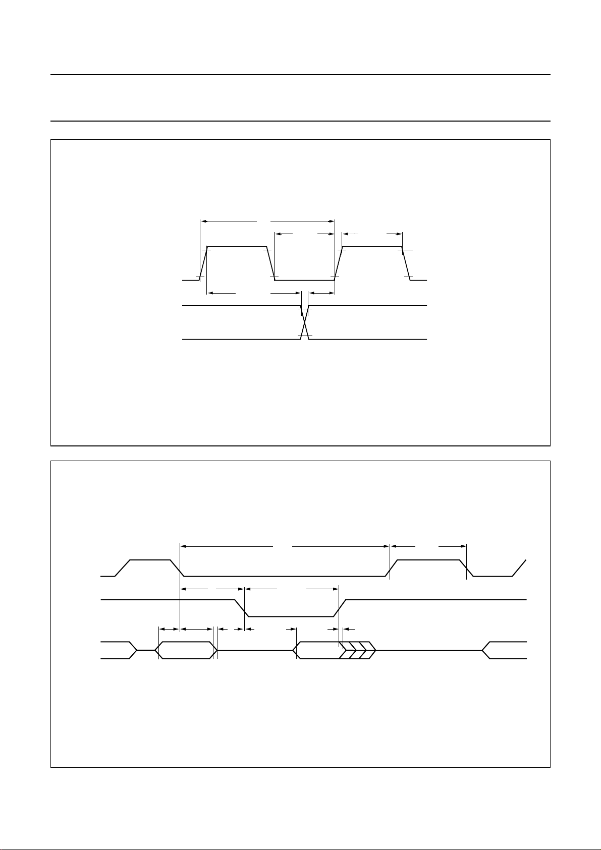
su(SCLK)
t
h(SCLK)
output clock period set by CLKPRE1
clock HIGH time −−− ns
clock LOW time −−− ns
set-up time − tbf − ns
hold time − tbf − ns
− 472.4 − ns
register
−−− ns
−−− ns
−−− ns
−−− ns
− tbf − ns
− tbf − ns
− tbf − ns
− tbf − ns
2001 apr 05 25
Page 26
Philips Semiconductors Preliminary specification
DSP for CD and DVD-ROM systems SAA7335
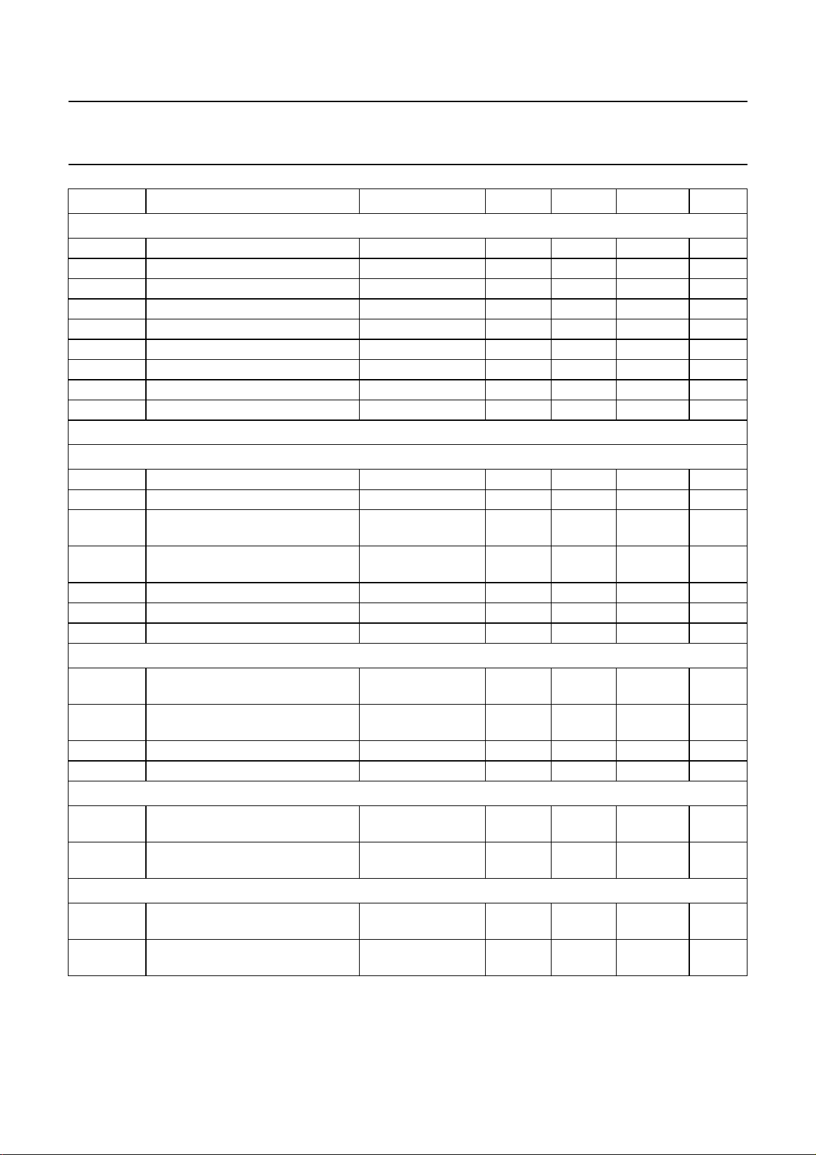
SYMBOL PARAMETER CONDITIONS MIN. TYP. MAX. UNIT
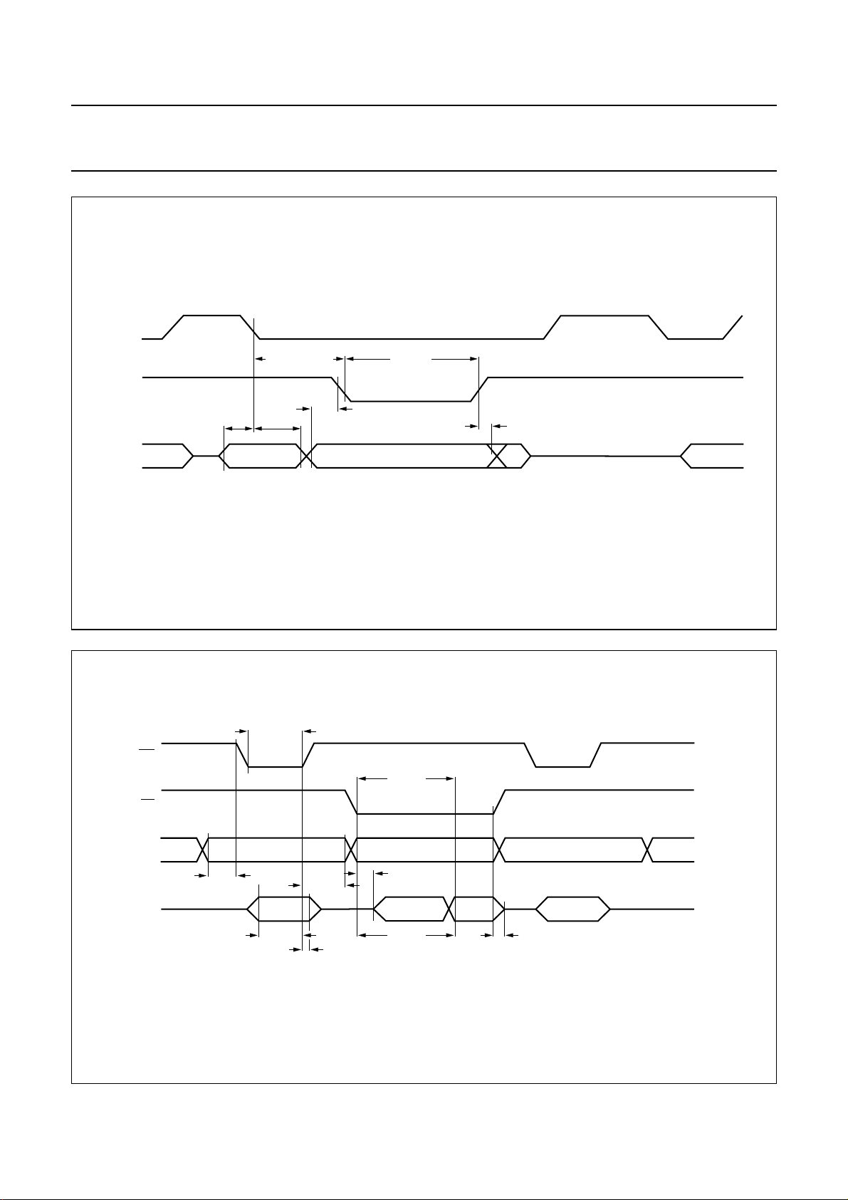
External RAM timing (see Figs 18 and 20)
t
AV-DV
t
OE-DV
t
W(W)
t
su(A)
t
h(A)
t
su(D-EW)
t
h(D-EW)
t
OE-DA
t
OD-DI
Microcontroller interface timing (see Figs 18 and 20)
INPUT ALE
t
su(A-ALE)
t
h(A-ALE)
t
ALEL
t
ALEH
t
d(ALEL-WRL)
t
r
t
f
INPUTS RDI AND WRI
t
IL(R/W)
t
IH(R/W)
t
r
t
f
READ MODE
t
d(RLDV)
t
d(RHDX)
WRITE MODE
t
su(QVWX)
t
h(WHQX)
address valid to data valid − tbf − ns
output enable to data valid − tbf − ns
write pulse width − tbf − ns
address set-up before start of write − tbf − ns
address hold after end of write − tbf − ns
data set-up to end of write − tbf − ns
data hold after end of write − tbf − ns
output enable to data active − tbf − ns
output disable to data inactive − tbf − ns
address set-up before ALE LOW 25 −− ns
address hold after ALE LOW 25 −− ns
input LOW time 1 × ADC
−− ns
CLK + 15
input HIGH time 1 × ADC
−− ns
CLK + 15
delay time ALE LOW to WR LOW −−− ns
rise time −−− ns
fall time −−240 ns
input LOW time 1 × ADC
−− ns
CLK + 15
input HIGH time 1 × ADC
−− ns
CLK + 15
rise time −−− ns
fall time −−240 ns
delay time RD LOW to DA0 to DA7
valid
delay time RD HIGH to DA0 to DA7
2 × ADC
−− ns
CLK + 35
15 −− ns
high-impedance
set-up time WR LOW to
−−− ns
DA0 to DA7
hold time WR HIGH to DA0 to DA7
3-state
2 × ADC
CLK + 25
−− ns
Notes
1. Timing reference voltage levels are 0.8 V and V
DDD
− 0.8 V.
2. Negative set-up time means that data may change after clock transition.
2001 apr 05 26
Page 27
Philips Semiconductors Preliminary specification
DSP for CD and DVD-ROM systems SAA7335
T
cy
SCLK
WCLK
DATA
MISC
t
h(SCLK)
t
SCKL
V – 0.8 V
DD
0.8 V
t
su(SCLK)
t
SCLKH
V – 0.8 V
DD
0.8 V
MGL507
handbook, full pagewidth
ALE
RDi
DA0
to
DA7
t
su(A-ALE)
t
h(A-ALE)
A0 to A7
Fig.17 I2S-bus timing.
t
ALEL
3
9
t
d(RLDV)
t
IH(R/W)
DATA OUT
t
d(RHDX)
t
ALEH
13
MGK253
Fig.18 Microcontroller interface timing; parallel read mode.
2001 apr 05 27
Page 28
Philips Semiconductors Preliminary specification
DSP for CD and DVD-ROM systems SAA7335
handbook, full pagewidth
ALE
WRi
DA0
to
DA7
handbook, full pagewidth
WE
t
su(A-ALE)
t
IH(R/W)
DATA IN
t
h(WHDX)
t
d(ALEL-WRL)
t
h(A-ALE)
A0 to A7
t
su(QVWX)
Fig.19 Microcontroller interface timing; parallel write mode.
t
W(W)
t
OE-DV
9
MGK254
OE
ADDRESS
DATA
A0
t
su(A)
t
su(D-EW)
A1 A2 A3 A4
t
OE-DA
X D2 D1
t
AD-DV
D1
t
h(A)
t
su(D-EW)
write cycle write cycleread cycle
Fig.20 External RAM timing.
2001 apr 05 28
t
OD-DI
MBH995
Page 29
Philips Semiconductors Preliminary specification
DSP for CD and DVD-ROM systems SAA7335
APPLICATION INFORMATION
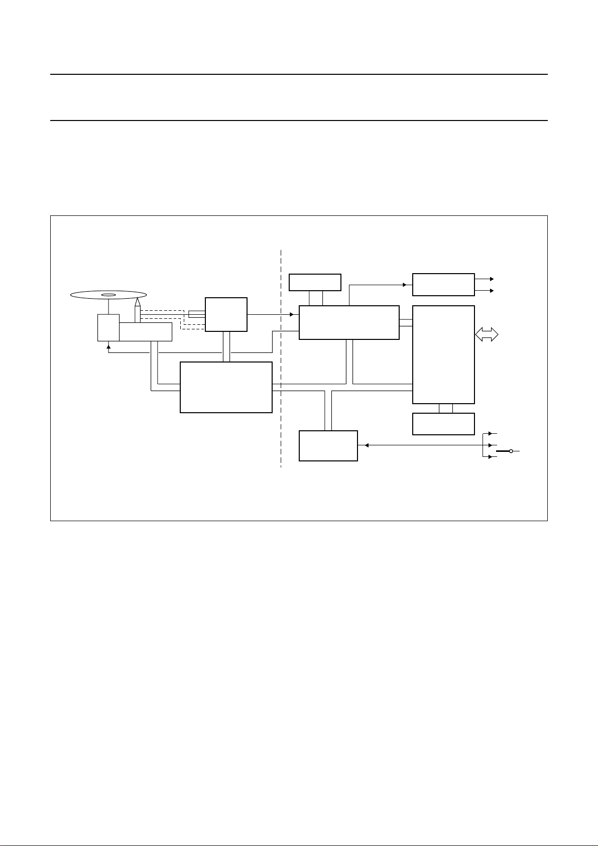
The complete data path chipset consists of two ICs, the CD decoder (or DSP) device and the block decoder/host
interface manager. In addition to these components a general purpose microcontroller and tracking servo is necessary
to produce a complete controller system for a DVD mechanism. The DSP, block decoder and microcontroller are shown
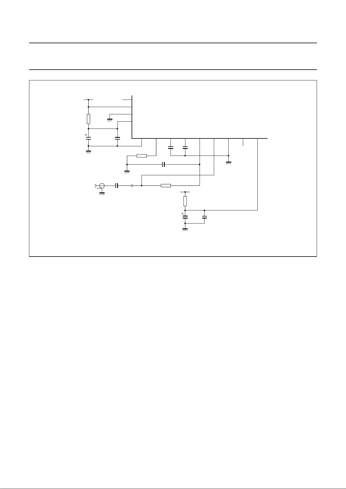
highlighted in Fig.21. An ADC application circuit is illustrated in Fig.22.
handbook, full pagewidth
MECHANISM/SERVO SUBSYSTEM DECODER/DATA PATH SUBSYSTEM
spindle
motor
laser
SLED/FOCUS
ACTUATORS
RAM BUFFER
PRE-
AMPLIFIER
C1-C2 ERROR CORRECTOR
SERVO CONTROL
PD TRACKING
(3 BEAM OPTIONAL FOR
BACKWARD CD-ROM
COMPATIBILITY)
SYSTEM
CONTROLLER
Fig.21 Basic DVD player block diagram.
CD-DSP
DEMODULATION
AUDIO DAC
BLOCK
DECODER
(FOR CD-ROM
COMPATIBILITY)
AND
HOST
INTERFACE
RAM BUFFER
MGK255
audio L/R
output
PC host
interface
user
key
switches
2001 apr 05 29
Page 30
Philips Semiconductors Preliminary specification
DSP for CD and DVD-ROM systems SAA7335
handbook, full pagewidth
AGND1
HF input
V
CC
R14
4.7 Ω
C11
47 µF
(50 V)
AGND1
TP1
AGND1
C16X6
2.2 nF
97
98
99
100
C10
100
123456789
nF
R29
10 kΩ
47 µF (50 V)
TP6
C19
R28
100 kΩ
C18
22
nF
C15
47 µF
(50 V)
Fig.22 ADC application circuit.
SAA7335
C17
22
nF
V
CC
R25
4.7 Ω
C14
100 nF
TP5
AGND1
MGK256
2001 apr 05 30
Page 31
Philips Semiconductors Preliminary specification
DSP for CD and DVD-ROM systems SAA7335
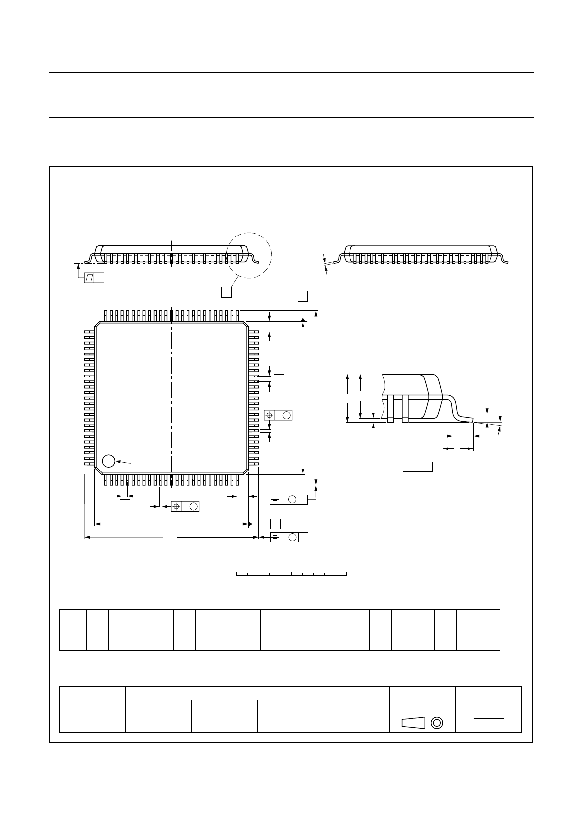
PACKAGE OUTLINE
LQFP100: plastic low profile quad flat package; 100 leads; body 14 x 14 x 1.4 mm
c
y
100
X
75
76
pin 1 index
1
e
w M
b
p
D
H
D
51
50
Z
E
26
25
Z
D
b
B
e
w M
p
v M
v M
A
H
E
E
A
B
A
2
A
A
1
detail X
SOT407-1
(A )
3
θ
L
p
L
0 5 10 mm
scale
DIMENSIONS (mm are the original dimensions)
UNIT
Note
1. Plastic or metal protrusions of 0.25 mm maximum per side are not included.
A
A1A2A3bpcE
max.
0.15
0.05
1.45
1.35
1.6
mm
OUTLINE
VERSION
SOT407-1 136E20 MS-026
0.27
0.17
0.20
0.09
0.25
IEC JEDEC EIAJ
(1)
(1) (1)(1)
D
14.1
13.9
REFERENCES
eH
14.1
13.9
0.5
16.25
15.75
2001 apr 05 31
H
D
E
16.25
15.75
LL
p
0.75
0.45
0.08 0.080.21.0
EUROPEAN
PROJECTION
Z
1.15
0.85
D
Zywv θ
E
1.15
0.85
o
7
o
0
ISSUE DATE
00-01-19
00-02-01
Page 32

Philips Semiconductors Preliminary specification
DSP for CD and DVD-ROM systems SAA7335
SOLDERING
Introduction
There is no soldering method that is ideal for all IC
packages. Wave soldering is often preferred when
through-hole and surface mounted components aremixed
on one printed-circuit board. However, wave soldering is
not always suitable for surface mounted ICs, or for
printed-circuits with high population densities. In these
situations reflow soldering is often used.
Thistextgivesaverybriefinsighttoacomplextechnology.
A more in-depth account of soldering ICs can be found in
our
“IC Package Databook”
Reflow soldering
Reflow soldering techniques are suitable for all LQFP
packages.
Reflow soldering requires solder paste (a suspension of
fine solder particles, flux and binding agent) to be applied
totheprinted-circuit board by screen printing, stencilling or
pressure-syringe dispensing before package placement.
Several techniques exist for reflowing; for example,
thermal conduction by heated belt. Dwell times vary
between 50 and 300 seconds depending on heating
method. Typical reflow temperatures range from
215 to 250 °C.
Preheating is necessary to dry the paste and evaporate
the binding agent. Preheating duration: 45 minutes at
45 °C.
Wave soldering
Wave soldering is not recommended for LQFP packages.
This is because of the likelihood of solder bridging due to
closely-spaced leads and the possibility of incomplete
solder penetration in multi-lead devices.
(order code 9398 652 90011).
If wave soldering cannot be avoided, the following
conditions must be observed:
• A double-wave (a turbulent wave with high upward
pressure followed by a smooth laminar wave)
soldering technique should be used.
• The footprint must be at an angle of 45° to the board
direction and must incorporate solder thieves
downstream and at the side corners.
Even with these conditions, do not consider wave
soldering LQFP packages LQFP48 (SOT313-2),
LQFP64 (SOT314-2) or LQFP80 (SOT315-1).
During placement and before soldering, the package must
be fixed with a droplet of adhesive. The adhesive can be
applied by screen printing, pin transfer or syringe
dispensing. The package can be soldered after the
adhesive is cured.
Maximum permissible solder temperature is 260 °C, and
maximum duration of package immersion in solder is
10 seconds, if cooled to less than 150 °C within
6 seconds. Typical dwell time is 4 seconds at 250 °C.
A mildly-activated flux will eliminate the need for removal
of corrosive residues in most applications.
Repairing soldered joints
Fix the component by first soldering two diagonallyopposite end leads. Use only a low voltage soldering iron
(less than 24 V) applied to the flat part of the lead. Contact
time must be limited to 10 seconds at up to 300 °C. When
using a dedicated tool, all other leads can be soldered in
one operation within 2 to 5 seconds between
270 and 320 °C.
2001 apr 05 32
Page 33

Philips Semiconductors Preliminary specification
DSP for CD and DVD-ROM systems SAA7335
DATA SHEET STATUS
PRODUCT
DATA SHEET STATUS
Objective data Development This data sheet contains data from the objective specification for product
Preliminary data Qualification This data sheet contains data from the preliminary specification.
Product data Production This data sheet contains data from the product specification. Philips
(1)
STATUS
(2)
DEFINITIONS
development. Philips Semiconductors reserves the right to change the
specification in any manner without notice.
Supplementary data will be published at a later date. Philips
Semiconductors reserves the right to change the specification without
notice, in order to improve the design and supply the best possible
product.
Semiconductors reserves the right to make changes at any time in order
to improve the design, manufacturing and supply. Changes will be
communicated according to the Customer Product/Process Change
Notification (CPCN) procedure SNW-SQ-650A.
Notes
1. Please consult the most recently issued data sheet before initiating or completing a design.
2. The product status of the device(s) described in this data sheet may have changed since this data sheet was
published. The latest information is available on the Internet at URL http://www.semiconductors.philips.com.
DEFINITIONS
Short-form specification The data in a short-form
specification is extracted from a full data sheet with the
same type number and title. For detailed information see
the relevant data sheet or data handbook.
Limiting values definition Limiting values given are in
accordance with the Absolute Maximum Rating System
(IEC 60134). Stress above one or more of the limiting
values may cause permanent damage to the device.
These are stress ratings only and operation of the device
attheseoratanyotherconditionsabovethosegiveninthe
Characteristics sections of the specification is not implied.
Exposure to limiting values for extended periods may
affect device reliability.
Application information Applications that are
described herein for any of these products are for
illustrative purposes only. Philips Semiconductors make
norepresentationorwarrantythatsuchapplicationswill be
suitable for the specified use without further testing or
modification.
DISCLAIMERS
Life support applications These products are not
designed for use in life support appliances, devices, or
systems where malfunction of these products can
reasonably be expected to result in personal injury. Philips
Semiconductorscustomersusingorsellingtheseproducts
for use in such applications do so at their own risk and
agree to fully indemnify Philips Semiconductors for any
damages resulting from such application.
Right to make changes Philips Semiconductors
reserves the right to make changes, without notice, in the
products, including circuits, standard cells, and/or
software, described or contained herein in order to
improve design and/or performance. Philips
Semiconductors assumes no responsibility or liability for
theuseofanyoftheseproducts,conveysnolicenceortitle
under any patent, copyright, or mask work right to these
products,andmakesnorepresentationsor warranties that
these products are free from patent, copyright, or mask
work right infringement, unless otherwise specified.
ICs with MPEG-2 functionality Use of this product in
any manner that complies with the MPEG-2 Standard is
expressly prohibited without a license under applicable
patents in the MPEG-2 patent portfolio, which license is
available from MPEG LA, L.L.C., 250 Steele Street, Suite
300, Denver, Colorado 80206.
2001 apr 05 33
Page 34

Philips Semiconductors Preliminary specification
DSP for CD and DVD-ROM systems SAA7335
PURCHASE OF PHILIPS I2C COMPONENTS
Purchase of Philips I
components in the I2C system provided the system conforms to the I2C specification defined by
Philips. This specification can be ordered using the code 9398 393 40011.
2
C components conveys a license under the Philips’ I2C patent to use the
2001 apr 05 34
Page 35

Philips Semiconductors Preliminary specification
DSP for CD and DVD-ROM systems SAA7335
NOTES
2001 apr 05 35
Page 36

Philips Semiconductors – a w orldwide compan y
Argentina: see South America
Australia: 3 Figtree Drive, HOMEBUSH, NSW 2140,
Tel. +61 2 9704 8141, Fax. +61 2 9704 8139
Austria: Computerstr. 6, A-1101 WIEN, P.O. Box 213,
Tel. +43 1 60 101 1248, Fax. +43 1 60 101 1210
Belarus: Hotel Minsk Business Center, Bld. 3, r. 1211, Volodarski Str. 6,
220050 MINSK, Tel. +375 172 20 0733, Fax. +375 172 20 0773
Belgium: see The Netherlands
Brazil: see South America
Bulgaria: Philips Bulgaria Ltd., Energoproject, 15th floor,
51 James Bourchier Blvd., 1407 SOFIA,
Tel. +359 2 68 9211, Fax. +359 2 68 9102
Canada: PHILIPS SEMICONDUCTORS/COMPONENTS,
Tel. +1 800 234 7381, Fax. +1 800 943 0087
China/Hong Kong: 501 Hong Kong Industrial Technology Centre,
72 Tat Chee Avenue, Kowloon Tong, HONG KONG,
Tel. +852 2319 7888, Fax. +852 2319 7700
Colombia: see South America
Czech Republic: see Austria
Denmark: Sydhavnsgade 23, 1780 COPENHAGEN V,
Tel. +45 33 29 3333, Fax. +45 33 29 3905
Finland: Sinikalliontie 3, FIN-02630 ESPOO,
Tel. +358 9 615 800, Fax. +358 9 6158 0920
France: 7 - 9 Rue du Mont Valérien, BP317, 92156 SURESNES Cedex,
Tel. +33 1 4728 6600, Fax. +33 1 4728 6638
Germany: Hammerbrookstraße 69, D-20097 HAMBURG,
Tel. +49 40 2353 60, Fax. +49 40 2353 6300
Hungary: Philips Hungary Ltd., H-1119 Budapest, Fehervari ut 84/A,
Tel: +36 1 382 1700, Fax: +36 1 382 1800
India: Philips INDIA Ltd, Band Box Building, 2nd floor,
254-D, Dr. Annie Besant Road, Worli, MUMBAI 400 025,
Tel. +91 22 493 8541, Fax. +91 22 493 0966
Indonesia: PTPhilips DevelopmentCorporation, Semiconductors Division,
Gedung Philips, Jl. Buncit Raya Kav.99-100, JAKARTA 12510,
Tel. +62 21 794 0040 ext. 2501, Fax. +62 21 794 0080
Ireland: Newstead, Clonskeagh, DUBLIN 14,
Tel. +353 1 7640 000, Fax. +353 1 7640 200
Israel: RAPAC Electronics, 7 Kehilat Saloniki St, PO Box 18053,
TEL AVIV 61180, Tel. +972 3 645 0444, Fax. +972 3 649 1007
Italy: PHILIPS SEMICONDUCTORS,Via Casati, 23 - 20052 MONZA (MI),
Tel. +39 039 203 6838, Fax +39 039 203 6800
Japan: Philips Bldg 13-37, Kohnan 2-chome, Minato-ku,
TOKYO 108-8507, Tel. +81 3 3740 5130, Fax. +81 3 3740 5057
Korea: Philips House, 260-199 Itaewon-dong, Yongsan-ku, SEOUL,
Tel. +82 2 709 1412, Fax. +82 2 709 1415
Malaysia: No. 76 Jalan Universiti, 46200 PETALING JAYA, SELANGOR,
Tel. +60 3 750 5214, Fax. +60 3 757 4880
Mexico: 5900 Gateway East, Suite 200, EL PASO, TEXAS 79905,
Tel. +9-5 800 234 7381, Fax +9-5 800 943 0087
Middle East: see Italy
Netherlands: Postbus 90050, 5600 PB EINDHOVEN, Bldg. VB,
Tel. +31 40 27 82785, Fax. +31 40 27 88399
New Zealand: 2 Wagener Place, C.P.O. Box 1041, AUCKLAND,
Tel. +64 9 849 4160, Fax. +64 9 849 7811
Norway: Box 1, Manglerud 0612, OSLO,
Tel. +47 22 74 8000, Fax. +47 22 74 8341
Pakistan: see Singapore
Philippines: Philips Semiconductors Philippines Inc.,
106 Valero St. Salcedo Village, P.O. Box 2108 MCC, MAKATI,
Metro MANILA, Tel. +63 2 816 6380, Fax. +63 2 817 3474
Poland: Al.Jerozolimskie 195 B, 02-222 WARSAW,
Tel. +48 22 5710 000, Fax. +48 22 5710 001
Portugal: see Spain
Romania: see Italy
Russia: Philips Russia, Ul. Usatcheva 35A, 119048 MOSCOW,
Tel. +7 095 755 6918, Fax. +7 095 755 6919
Singapore: Lorong 1, Toa Payoh, SINGAPORE 319762,
Tel. +65 350 2538, Fax. +65 251 6500
Slovakia: see Austria
Slovenia: see Italy
South Africa: S.A. PHILIPS Pty Ltd., 195-215 Main Road Martindale,
2092 JOHANNESBURG, P.O. Box 58088 Newville 2114,
Tel. +27 11 471 5401, Fax. +27 11 471 5398
South America: Al. Vicente Pinzon, 173, 6th floor,
04547-130 SÃO PAULO, SP, Brazil,
Tel. +55 11 821 2333, Fax. +55 11 821 2382
Spain: Balmes 22, 08007 BARCELONA,
Tel. +34 93 301 6312, Fax. +34 93 301 4107
Sweden: Kottbygatan 7, Akalla, S-16485 STOCKHOLM,
Tel. +46 8 5985 2000, Fax. +46 8 5985 2745
Switzerland: Allmendstrasse 140, CH-8027 ZÜRICH,
Tel. +41 1 488 2741 Fax. +41 1 488 3263
Taiwan: Philips Semiconductors, 5F, No. 96, Chien Kuo N. Rd., Sec. 1,
TAIPEI, Taiwan Tel. +886 2 2134 2451, Fax. +886 2 2134 2874
Thailand: PHILIPS ELECTRONICS (THAILAND) Ltd.,
60/14 MOO 11, Bangna Trad Road KM. 3, Bagna, BANGKOK 10260,
Tel. +66 2 361 7910, Fax. +66 2 398 3447
Turkey: Yukari Dudullu, Org. San. Blg., 2.Cad. Nr. 28 81260 Umraniye,
ISTANBUL, Tel. +90 216 522 1500, Fax. +90 216 522 1813
Ukraine: PHILIPS UKRAINE, 4 Patrice Lumumba str., Building B, Floor 7,
252042 KIEV, Tel. +380 44 264 2776, Fax. +380 44 268 0461
United Kingdom: Philips Semiconductors Ltd., 276 Bath Road, Hayes,
MIDDLESEX UB3 5BX, Tel. +44 208 730 5000, Fax. +44 208 754 8421
United States: 811 East Arques Avenue, SUNNYVALE, CA 94088-3409,
Tel. +1 800 234 7381, Fax. +1 800 943 0087
Uruguay: see South America
Vietnam: see Singapore
Yugoslavia: PHILIPS, Trg N. Pasica 5/v, 11000 BEOGRAD,
Tel. +381 11 3341 299, Fax.+381 11 3342 553
For all other countries apply to: Philips Semiconductors,
Marketing Communications, Building BE-p, P.O. Box 218, 5600 MD EINDHOVEN,
The Netherlands, Fax. +31 40 27 24825
© Philips Electronics N.V. SCA
All rights are reserved. Reproduction in whole or in part is prohibited without the prior written consent of the copyright owner.
The information presented in this document does not form part of any quotation or contract, is believed to be accurate and reliable and may be changed
without notice. No liability will be accepted by the publisher for any consequence of its use. Publication thereof does not convey nor imply any license
under patent- or other industrial or intellectual property rights.
2001
Internet: http://www.semiconductors.philips.com
72
Printed in The Netherlands 753503/02/pp36 Date of release: 2001 apr 05 Document order number: 9397 750 08202
 Loading...