

Page 1

INTEGRATED CIRCUITS
DATA SH EET
SAA7282
Terrestrial Digital Sound Decoder
(TDSD2)
Product specification
File under Integrated Circuits, IC02
July 1993
Page 2

Philips Semiconductors Product specification
Terrestrial Digital Sound Decoder (TDSD2) SAA7282
FEATURES
• Full EBU NICAM 728 specification decoder
• Microcomputer controlled via I2C-bus
• Automatic decoding and output configuration depending
upon transmission:
– digital stereo
– digital mono and data
– 2 independent mono signals
• On board RAM for de-interleaving and 10 to 14-bit word
expansion
• Automatic mute function which silences the digital data
and switches to FM sound (if valid) when error rate
exceeds user definable limit
• User mute function (
MUTE pin) to enable user to
perform muting to their own software algorithm if
required, or to simply silence the output
• 4 times over-sampling digital filter
• Selectable digital de-emphasis
• 256 times over-sampling Noise Shapers
• Fully integrated 1-bit DACs
• Integrated switching networks allowing selection
between NICAM Sound, FM Sound or external
“Daisy-Chain” input
• Digital Audio Interface conforming with EBU/IEC 958
• I2C-bus transceiver enabling a master device to read
– status information
– error count byte
– additional data bits
and write:
– switch control codes
– decoder control
– upper and lower error rate limits.
APPLICATIONS
• Television receivers
• Video cassette recorders.
GENERAL DESCRIPTION
Performing all digital decoding functions for a NICAM 728
digital stereo sound system, the SAA7282 is a highly
integrated CMOS circuit which only requires a DQPSK
(Differential Quadrature Phase Shift Keying) demodulator
(TDA8732) and minimum external components to achieve
a full NICAM solution.
The device may also be interfaced to other DQPSK
demodulators.
QUICK REFERENCE DATA
SYMBOL PARAMETER MIN. TYP. MAX. UNIT
V
DD
I
DD
f
XTAL
T
amb
positive supply voltage 4.5 5.0 5.5 V
supply current − 50 100 mA
crystal frequency − 8.192 − MHz
operating ambient temperature 0 − 70 °C
ORDERING INFORMATION
EXTENDED TYPE
NUMBER
PINS PIN POSITION MATERIAL CODE
PACKAGE
SAA7282ZP 32 DIL32SHR plastic SOT232A
SAA7282GP 44 QFP plastic SOT205AG
Note
1. SAA7282ZP: 32-DIL32SHR; plastic (SOT232A); SOT232-1; 1996 November 28.
2. SAA7282GP: 44-QFP; plastic (SOT205AG); SOT205-1; 1996 November 28.
July 1993 2
(1)
(2)
Page 3
This text is here in white to force landscape pages to be rotated correctly when browsing through the pdf in the Acrobat reader.This text is here in
_white to force landscape pages to be rotated correctly when browsing through the pdf in the Acrobat reader.This text is here inThis text is here in
white to force landscape pages to be rotated correctly when browsing through the pdf in the Acrobat reader. white to force landscape pages to be ...
July 1993 3
Philips Semiconductors Product specification
Terrestrial Digital Sound Decoder (TDSD2) SAA7282
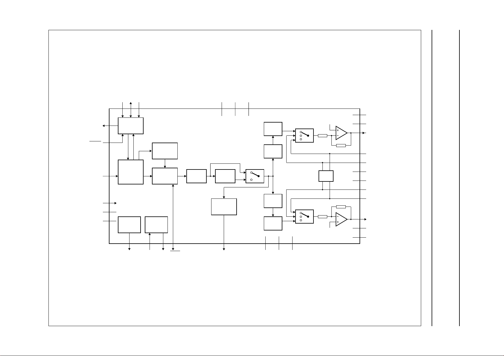
PORT2
RESET
DATA
i.c.
V
DD
V
SS
5
2
32
26
27
29
SDA
ADSELSCL
4
6
3
2
I C
AUTO
MUTE
NICAM
728
DECODING
FREQ.
SYNTH.
13031
SWITCHING
XTAL
OSC
XIN XOUTPCLK
DIGITAL
7
MUTE
V
DAC
18
SAA7282ZP
FILTER DE-EMPH
DIGITAL
AUDIO
INTERFACE
28
DOBM V
CDL
INTL
20
19
1-BIT
DAC
NOISE
SHAPER
NOISE
SHAPER
1-BIT
DAC
17
REF
CDR
15
16
INTR
VRC
BIAS
VRC
25
24
23
21
22
10
11
13
14
12
MLB152
V
DDAL
V
SSAL
OPL
FML
EXTL
VRO
VRC
EXTR
FMR
OPR
8
V
DDAR
9
V
SSAR
handbook, full pagewidth
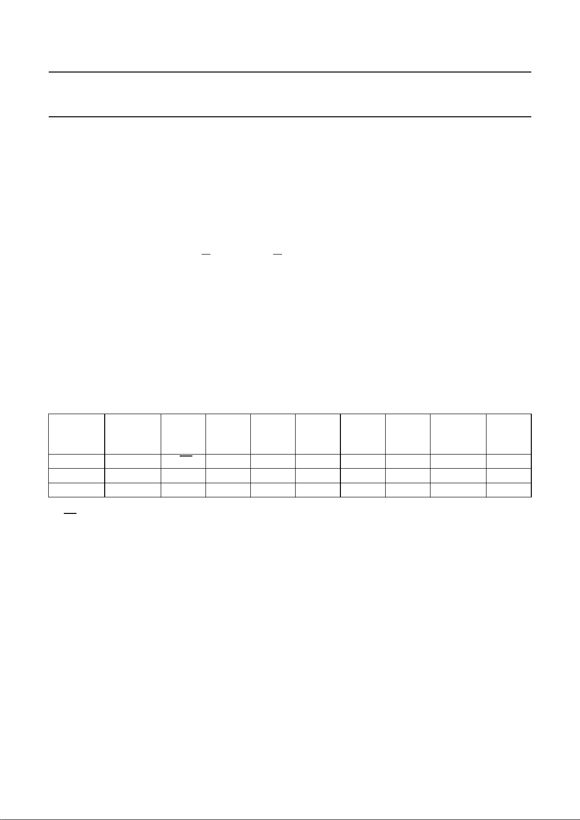
Fig.1 Block diagram; pin numbering for SOT232A.
Page 4
Philips Semiconductors Product specification
Terrestrial Digital Sound Decoder (TDSD2) SAA7282
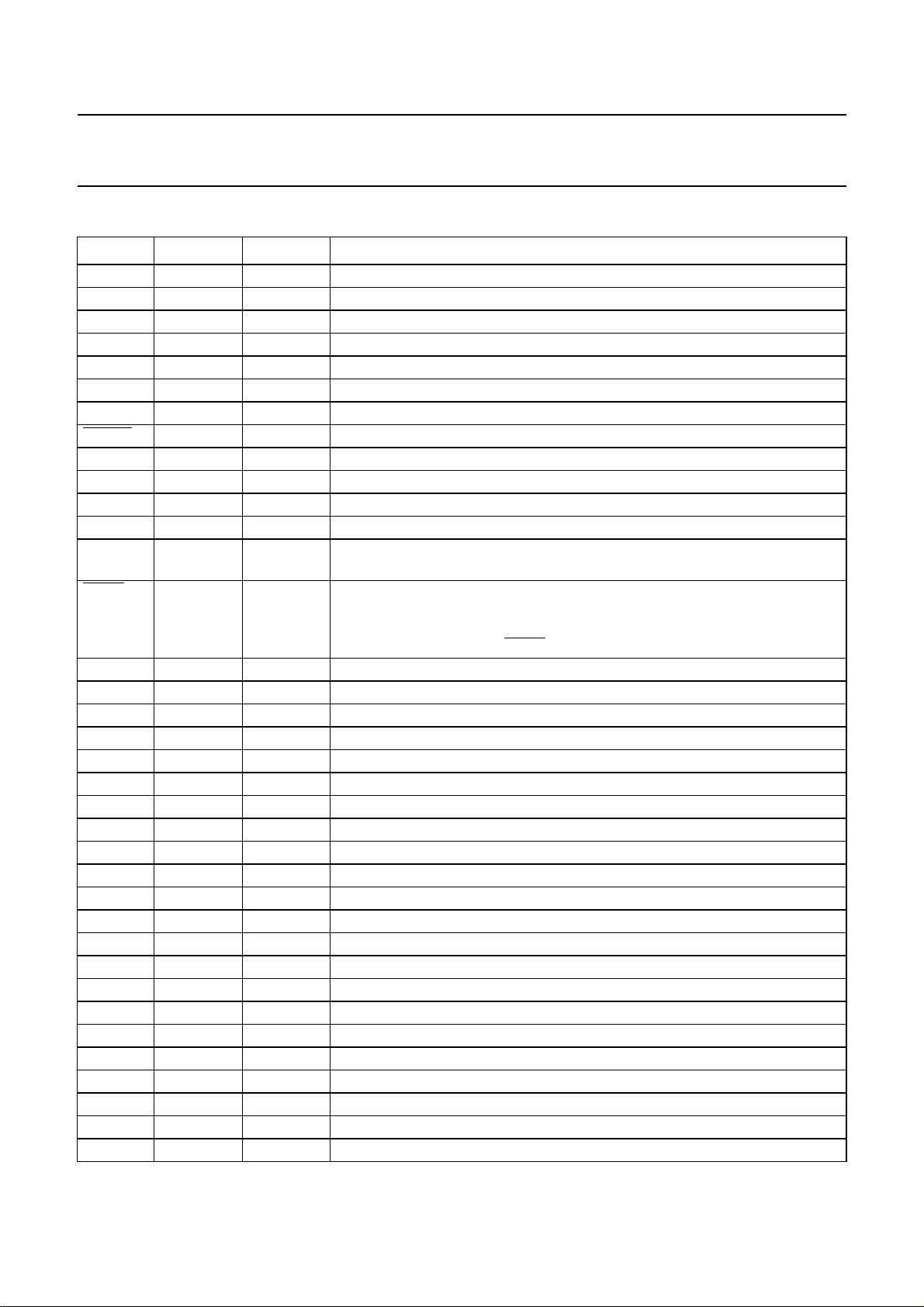
PINNING
SYMBOL SOT205AG SOT232A DESCRIPTION
DOBM 1 28 digital audio interface output
V
SS
n.c. 3 − not connected
XIN 4 30 crystal input at 256fs (8.192 MHz)
XOUT 5 31 crystal output at 256fs (8.192 MHz)
DATA 6 32 serial data input at 728 kbits/s from DQPSK demodulator
PCLK 7 1 output clock at 728 kHz to DQPSK demodulator
RESET 8 2 active LOW reset; used to set the device in a valid initial condition
SCL 9 3 clock input for I
SDA 10 4 data port for I
PORT2 11 5 output mirroring the I
n.c. 12 − not connected
ADSEL 13 6 I2C-bus slave address selection input; allows selection of one of two separate
MUTE 14 7 active LOW mute input; when set LOW, sets the digital data to zero and either
n.c. 15 to 17 − not connected
V
DDAR
V
SSAR
VRO 20 10 internal reference voltage buffer output
VRC 21 11 internal reference voltage buffer HIGH impedance node
n.c. 22 − not connected
OPR 23 12 analog output from the right audio channel
EXTR 24 13 external analog input to the right audio channel
FMR 25 14 FM sound input to the right audio channel
INTR 26 15 integrator output from the right audio channel
CDR 27 16 integrator connection to an external damping capacitor
n.c. 28 − not connected
V
REF
V
DAC
CDL 31 19 integrator connection to an external damping capacitor
INTL 32 20 integrator output from the left audio channel
FML 33 21 FM sound input to the left audio channel
EXTL 34 22 external analog input to the left audio channel
OPL 35 23 analog output from the left audio channel
n.c. 36 − not connected
V
SSAL
V
DDAL
2 29 ground connection for the digital section
2
C control bus
2
C control bus, input/open drain output
2
C control register bit PORT2
slave addresses, defaults to logic 1
silences the output or switches it to analog FM, depending on the status of
MUTEDEF (control bit in the I2C register) and RSSF; overridden by automute
(if automute is used, then MUTE is automatically pulled LOW)
18 8 analog supply voltage for the right audio channel
19 9 analog ground connection for the right audio channel
29 17 reference voltage input; 2.5 V (typical)
30 18 quiet VSS to DACs
37 24 analog ground connection for the left audio channel
38 25 analog supply voltage for the left audio channel
July 1993 4
Page 5
Philips Semiconductors Product specification
Terrestrial Digital Sound Decoder (TDSD2) SAA7282
SYMBOL SOT205AG SOT232A DESCRIPTION
n.c. 39 to 41 − not connected
i.c. 42 26 internally connected; must be left open-circuit in application
n.c. 43 − not connected
V
DD
44 27 digital supply voltage
handbook, halfpage
PCLK
RESET
SCL
SDA
PORT2
ADSEL
MUTE
V
DDAR
V
SSAR
VRO
VRC
OPR
EXTR
FMR
INTR
CDR
1
2
3
4
5
6
7
8
SAA7282ZP
9
10
11
12
13
14
15
16
MLB153
32
31
30
29
28
27
26
25
24
23
22
21
20
19
18
17
DATA
XOUT
XIN
V
SS
DOBM
V
DD
i.c.
V
DDAL
V
SSAL
OPL
EXTL
FML
INTL
CDL
V
DAC
V
REF
Fig.2 Pin configuration (SOT232A).
July 1993 5
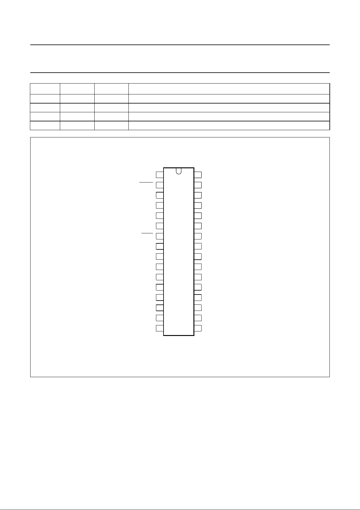
Page 6
Philips Semiconductors Product specification
Terrestrial Digital Sound Decoder (TDSD2) SAA7282
handbook, full pagewidth
DOBM
V
SS
n.c.
XIN
XOUT
DATA
PCLK
RESET
SCL
SDA
PORT2
DD
n.c.
V
44
43
1
2
3
4
5
6
7
8
9
10
11
12
13
n.c.
ADSEL
i.c.
42
14
MUTE
n.c.
n.c.
41
SAA7282GP
15
n.c.
n.c.
DDAL
SSAL
38
18
DDAR
V
37
19
SSAR
V
n.c.
36
20
VRO
OPL
35
21
VRC
EXTL
34
22
n.c.
33
32
31
30
29
28
27
26
25
24
23
MLB154
FML
INTL
CDL
V
DAC
V
REF
n.c.
CDR
INTR
FMR
EXTR
OPR
n.c.
V
40
39
16
17
n.c.
V
Fig.3 Pin configuration (SOT205AG).
July 1993 6
Page 7
Philips Semiconductors Product specification
Terrestrial Digital Sound Decoder (TDSD2) SAA7282
I2C-BUS FORMATS
The SAA7282 contains an I2C-bus slave transceiver permitting a master device to:
• Read decoder status information derived from the transmitted digital audio signal
• Read an error count byte to determine the bit error rate for user mute purposes and to indicate quality of NICAM signal
• Read additional transmitted data bits. Their purpose has yet to be defined but accessibility is provided to allow future
services to be implemented in receiver software
• Write control codes to select the available analog switching configurations
• Write upper and lower error count limits for automatic muting function
The device slave address is A(7:1)(R/W) = 101101X(R/W). An ADSEL pin is provided to allow selection of one of two
different slave addresses via programmable address bit A1. (X = ADSEL logic level).
The SAA7282 does not acknowledge the I2C-bus general call address.
The slave receiver format is:
S SLAVE_ADDR.0 ACK SUB_ADDR ACK DATA BYTE ACK P
<−n bytes−>
Where S = start, ACK = acknowledge, P = stop.
Auto-increment of the sub-address is provided with wrap-around from 02 (HEX) to 00 (HEX).
The slave receiver data byte format, as a function of sub-address, is as shown in Table 1.
Table 1 Slave receiver data byte.
SUB-
ADDRESS
00 90 M1/M2 DMSEL SSWIT3 SSWIT2 SSWIT1 PORT2 MUTEDEF AMDIS
01 50 EMAX7 EMAX6 EMAX5 EMAX4 EMAX3 EMAX2 EMAX1 EMAX0
10 14 EMIN7 EMIN6 EMIN5 EMIN4 EMIN3 EMIN2 EMIN1 EMIN0
M1/
M2
This bit in conjunction with DMSEL bit, determines the output configuration in dual mono mode (see Table 2).
Power-on resets to logic 1.
DMSEL
This bit determines whether one or both of the dual mono signals are output (see Table 2). Power-on resets to logic 0.
PORT2
PORT2 controls a bit out, providing direct access to a dedicated output pin (PORT2) via the I2C-bus. See Table 3.
Power-on resets to logic 0.
RESET
VALUE
HEX
D7 D6 D5 D4 D3 D2 D1 D0
SSWIT3/2/1
These bits control the analog switching, selecting between the FM, external, and NICAM signals. With the NICAM source
the signals select whether the de-emphasis is performed and what gain is applied after the filtering and de-emphasis
stage. The signal states and their meaning are listed in Table 4. Power-on resets to 0/1/0.
July 1993 7
Page 8
Philips Semiconductors Product specification
Terrestrial Digital Sound Decoder (TDSD2) SAA7282
AMOGMDIS
This bit enables and disables the automute function (which
is activated according to the error limit registers).
Power-on resets to enabled (i.e. AMDIS = logic 0). AMDIS
should be disabled for the user definable mute (MUTE) to
be used.
MUTEDEF
This defines the operation of the user definable MUTE pin
when it is pulled LOW externally. If MUTEDEF is HIGH and
RSSF = logic 1, the output of the device is switched to FM
input. If MUTEDEF is HIGH and RSSF = logic 0, or if
MUTEDEF is LOW, the output is muted. Power on resets
to LOW.
Table 2 Output as a function of M1/
DMSEL M1/
0 0 selects DIGITAL; L = M2, R = M2
0 1 selects DIGITAL; L = M1, R = M1
1 0 selects DIGITAL; L = M2, R = M1
1 1 selects DIGITAL; L = M1, R = M2
M2 and DMSEL.
M2 FUNCTION
ERROR LIMIT REGISTERS
UPPER ERROR LIMIT REGISTER
This defines the number of errors in 128 ms period which
will cause automute to switch IN. User definable, but
power on resets to 50 Hex.
LOWER ERROR LIMIT REGISTER
This defines the number of errors in 128 ms period which
will cause automute to switch OUT. User definable, but
power on resets to 14 Hex.
Table 3 Port 2 control.
PORT2 PIN OUTPUT STATE
0 LOW
1 HIGH
Table 4 SSWIT signal states and function.
SSWIT3 SSWIT2 SSWIT1 FUNCTION
0 0 0 NICAM source de-emphasis switched out, no gain
0 0 1 NICAM source de-emphasis switched in, no gain
0 1 0 NICAM source de-emphasis switched in, −6 dB gain; power-on reset state
0 1 1 NICAM source de-emphasis switched in, +12 dB gain
1 x 0 external inputs switched in, no change to previous de-emphasis/gain setting
1 x 1 FM inputs switched in, no change to previous de-emphasis/gain setting
Note
1. Where x = don’t care.
(1)
July 1993 8
Page 9

Philips Semiconductors Product specification
Terrestrial Digital Sound Decoder (TDSD2) SAA7282
Slave Transmitter
The slave transmitter formats are illustrated thus:
• S SLAVE_ADDR.1 A STATUS_BYTE NA P
In this format the bus master reads the STATUS_BYTE once.
• S SLAVE_ADDR.1 A STATUS_BYTE A ERROR_BYTE NA P
In this format the bus master reads two bytes of STATUS_BYTE and ERROR_BYTE.
• S SLAVE_ADDR.1 A STATUS_BYTE A ERROR_BYTE A AD_BYTE_0 A AD_BYTE_1 NA P
In this format the bus master reads four bytes of STATUS_BYTE, ERROR BYTE and two additional bytes, AD_BYTE_0
and AD_BYTE_1. The additional data bytes contain the eleven additional data bits AD0 to AD10 together with
information regarding their status.
Where NA = no acknowledge.
Table 5 Data byte formats.
BYTE D7 D6 D5 D4 D3 D2 D1 D0
STATUS_BYTE PONRES S/
ERROR_BYTE E7 E6 E5 E4 E3 E2 E1 E0
AD_BYTE_0 AD7 AD6 AD5 AD4 AD3 AD2 AD1 AD0
AD_BYTE_1 OVW SAD 0 CI2 CI1 AD10 AD9 AD8
MD/S VDSP RSSF OS AM CFC
The bits may be defined as follows:
PONRES
This bit is a power-on reset detection bit. It is set HIGH
after a power-on reset or supply reduction and is cleared
LOW when the STATUS_BYTE is read.
S/M (stereo/mono indication)
S/M = logic 1 indicating an incoming stereo transmission.
S/M = logic 0 indicating that the incoming transmission is
not stereo.
D/S (dual/single mono indication)
D/S = logic 1 indicating an incoming dual mono
transmission.
D/S = logic 0 indicating that the incoming transmission is
not dual mono.
VDSP
This bit indicates that the decoded signal is valid digital
sound. When VDSP = logic 0 the incoming transmission
carries either a 704 kbit/s transparent data channel or a
currently undefined format and the device automatically
switches to FM regardless of RSSF.
RSSF
RSSF is the reserve sound switching flag indication equal
to the C4 bit in the NICAM transmission. RSSF = logic 1
when the FM sound signal is carrying the same
programme material as the digitally modulated carrier
(specifically the M1 signal in the event of a dual mono
transmission). RSSF = logic 0 when the FM signal is not
reproduced within the digital signal.
OS
This bit provides an active LOW indication that the decoder
is out of sync. If OS = logic 1 the decoder is frame
synchronized and has obtained C0 (16 frame) sync.
If OS = logic 0, the decoder is out of sync and the indicator
bits are as given in Table 6.
AM
This bit indicates when the automuting function has
switched from the NICAM sound to the conventional FM
sound. This enables the software controller to display the
relevant information to the customer, for example, on
screen display. If AM bit = logic 0 no switching has been
carried out by the automuting function. If AM bit = logic 1
then the automuting function has switched to the FM
inputs.
July 1993 9
Page 10

Philips Semiconductors Product specification
Terrestrial Digital Sound Decoder (TDSD2) SAA7282
CFC
Signals a change of configuration at the 16-frame
boundary. It is cleared to logic 1 by the I2C-bus reading the
status register.
E7 to E0
This is an error count byte which counts the number of
error flags in a 128 ms period. The register is updated
every 128 ms.
AD10 to AD0
These are the additional data bits from the transmission
and are updated every 1 ms.This provides a data capacity
of 11 kbit/s.
SAD
SAD is the 'status additional data' bit. This is set to logic 1
when new bits AD10 to AD0 are latched into the I2C-bus
registers. It is automatically reset to logic 0 when
AD_BYTE_1 is read by the bus master.
Table 6 Indicator bits functional truth table.
TRANSMISSION C1 C2 C3 S/M D/S VDSP OS
Stereo 0 0 0 1 0 1 1
M1 + M2 0 1 0 0 1 1 1
M1 + data 1 0 0 0 0 1 1
Transparent data 1 1 0 0 0 0 1
Any currently undefined combination of C1, C2, C3 0 0 0 1
Decoder unsynchronized (OS = logic 0) note 1 note 1 0 0
OVW
OVW is the overwrite indicator for the additional data.
This bit is set when the transmission overwrites additional
data bits which have not been read by the bus master.
This bit is automatically reset to logic 0 when AD_BYTE_1
is read by the bus master.
CI1 to CI2
These represent the CI bits which are extracted by a
majority logic process from the parity checks of the last ten
samples in a frame (samples 55 to 64). CI1 will be
conveyed by the parity grouping of samples 55 to 59 and
CI2 will be conducted by the parity grouping of samples 60
to 64. Both parity groups will be even for UK transmissions
such that CI2 = logic 0 and CI1 = logic 0. The
transmissions of countries following the specification
issued by the EBU (Document SPB424;
transmissions in terrestrial television”
even parity groups, thus providing an additional 2 kbit/s
data capacity.
“Digital sound
) will allow odd or
Note
1. Holds last value before synchronization loss or stereo (S/
since power-on reset.
July 1993 10
M = logic 1; D/S = logic 0) if synchronization not achieved
Page 11

Philips Semiconductors Product specification
Terrestrial Digital Sound Decoder (TDSD2) SAA7282
DIGITAL AUDIO INTERFACE IEC/EBU 958
Block structure
The output is grouped into a block of 192 consecutive
frames providing, for each channel the 192 channel status
data bits. The start of a block is designated by a special
sub-frame preamble.
Frame structure
Each frame is uniquely composed of two sub-frames. The
rate of transmission of frames corresponds exactly to the
source sampling frequency. In the 2-channel operation,
samples taken from both channels are transmitted by time
multiplexing in consecutive sub-frames. Sub-frames
related to Channel 1 (left or 'A' channel in stereophonic
operation and primary channel in monophonic operation)
normally use preamble M. However the preamble is
changed to preamble B once every 192 frames. This
defines the block structure used to organize the channel
status information. Sub-frames of Channel 2 (right or 'B'
channel in stereophonic operation and secondary channel
in monophonic operation) always use preamble W.
Sub-frame structure
Each frame is divided into 32 time-slots numbered 0 to 31.
Time-slots 0 to 3 carry one of three permitted preambles.
These are used to affect synchronization of sub-frames,
frames and blocks.
Time-slots 4 to 27 carry the audio sample word in linear
two's complement representation. The most significant bit
is carried by time-slot 27.
Time-slot 28 carries the validity flag associated with the
audio sample word. This flag is set to logic 0 if the audio
sample is reliable. If set to logic 1 then the sample is
unreliable.
Time-slot 29 carries one bit of the user data channel. In
this application this is not used and so is set to logic 0.
Time-slot 30 carries one bit of the channel status world
associated with the audio channel transmitted in the same
sub-frame.
Time-slot 31 carries a parity bit such that time-slots 4 to 31
inclusive will carry an even number of ones and an even
number of zeros.
handbook, full pagewidth
handbook, full pagewidth
M channel 1
0
sync
preamble
MLB156
W
frame 191
channel 2
B
channel 1
sub-frame
start of block
W
frame 0
channel 2
sub-frame
Fig.4 Frame format.
4
31112
L
logical 0 bits audio sample word
S
B
Fig.5 Sub-frame format.
M
channel 1
frame 1
validity flag
user data = logic 0
channel status
parity bit
W
channel 2
28 3127
M
S
VUCP
B
MLB155
July 1993 11
Page 12

Philips Semiconductors Product specification
Terrestrial Digital Sound Decoder (TDSD2) SAA7282
Channel coding
Time-slots are encoded as biphase mark data. Each bit
transmitted is represented by a symbol comprising two
consecutive binary states. The first state of a symbol is
always different from the second state of the previous
symbol. The second state of the symbol is identical to the
first if the bit being transmitted is logic 0, however it is
different if the bit is logic 1 (see Table 7).
Table 7 Channel coding.
Preceding state 0 1
Transmitted bit Channel coding
01100
11001
The preambles preceding each digital audio sample are used to indicate the beginning of a sample as follows:
• Preamble B indicates the start of Channel A data and the beginning of a block
• Preamble M indicates the start of Channel A data but not the beginning of a block
• Preamble W indicates the start of Channel B data.
Preambles
Preambles are specific patterns providing synchronization
and identification of the sub-frames and blocks. A set of
three preambles is used. These preambles are transmitted
in the time allocated to four time-slots and are represented
by eight successive states. The first state of the preamble
is always different from the second state of the previous
symbol. Depending on this state the preambles are as
shown in Table 8.
Table 8 Preambles.
Preceding state 0 1
Preamble Channel coding
B 11101000 00010111
M 11100010 00011101
W 11100100 00011011
Channel status
The channel status information is organized in 192-bit words. The first bit of each word is carried in the frame with
Preamble B. The 192-bit word is organized into sections as shown in Table 9.
Table 9 Channel status codes.
BIT CODE DESCRIPTION
0 0 consumer
1 0 sound data
2 1 digital copy permitted
3, 4 00 indicates digital de-emphasis switched in
11 indicates digital de-emphasis switched out
50
6, 7 00
8 to 15 00110001 category code
16 to 19 0000 source code (don't care)
20 to 23 0000 channel number (don't care)
24 to 27 1100 sampling frequency (32 kHz)
28, 29 00 clock accuracy (level II)
30 to 191 all 0s
July 1993 12
Page 13

Philips Semiconductors Product specification
Terrestrial Digital Sound Decoder (TDSD2) SAA7282
LIMITING VALUES
In accordance with the Absolute Maximum System (IEC 134).
SYMBOL PARAMETER CONDITIONS MIN. MAX. UNIT
V
DD
V
I(max)
V
O(max)
I
IOK
I
O(max)
T
amb
T
stg
V
stat
Notes
1. All V
2. Electrostatic handling is equivalent to discharging a 100 pF capacitor via a 1.5 kΩ series resistor with a 15 ns rise
time.
3. 1000 V V
supply voltage (all supplies) note 1 −0.5 +6.5 V
maximum input voltage (any input) −0.5 VDD+0.5 V
maximum output voltage −0.3 VDD+0.5 V
DC input or output diode current −±20 mA
output current (each output) −±10 mA
ambient operating temperature 0 +70 °C
storage temperature −55 +125 °C
electrostatic handling notes 2 and 3 −2000 +2000 V
and VSS connections must be made externally to the same power supply.
DD
pin.
SSAL
July 1993 13
Page 14

Philips Semiconductors Product specification
Terrestrial Digital Sound Decoder (TDSD2) SAA7282
CHARACTERISTICS
V
= 4.5 to 5.5 V; T
DD
SYMBOL PARAMETER CONDITIONS MIN. TYP. MAX. UNIT
Supplies
V
DD
I
DD
V
SS,VSSAL
V
SSAR,VDAC
,
V
DDAL
V
DDAR
supply voltage see Fig.9 4.5 5.0 5.5 V
total supply current − 50 100 mA
ground supply voltage 0 − 0V
analog supply voltage see Fig.9 4.5 5.0 5.5 V
Digital inputs
DATA
V
IL
V
IH
I
LI
C
I
LOW level input voltage 0 − 0.8 V
HIGH level input voltage 2.0 − V
input leakage current −10 − +10 µA
input capacitance −−10 pF
ADSEL (this pin is internally pulled HIGH when not connected)
V
IL
V
IH
Z
I
C
I
LOW level input voltage 0 − 0.8 V
HIGH level input voltage 2.0 − V
input impedance − 50 − kΩ
input capacitance −−10 pF
RESET (Schmitt trigger input)
V
IL
V
IH
V
hys
LOW level input voltage 0 − 1.5 V
HIGH level input voltage 3.0 − V
hysteresis 0.05V
SCL
V
IL
V
IH
V
hys
I
LI
C
I
LOW level input voltage 0 − 1.5 V
HIGH level input voltage 3.0 − V
hysteresis 0.05V
input leakage current −10 −+10 µA
input capacitance −−10 pF
= 0 to +70 °C; unless otherwise specified.
amb
DD
DD
DD
DD
DD
V
V
V
−− V
DD
V
−− V
July 1993 14
Page 15

Philips Semiconductors Product specification
Terrestrial Digital Sound Decoder (TDSD2) SAA7282
SYMBOL PARAMETER CONDITIONS MIN. TYP. MAX. UNIT
Digital input/output
SDA
V
IL
V
IH
V
hys
I
LI
C
I
V
OL
C
L
MUTE I/O (this pin has an internal pull-up)
V
IL
V
IH
C
I
V
OL
V
OH
C
L
Z
I
Digital outputs
PORT2, PCLK, DOBM
V
OL
V
OH
C
L
Crystal oscillator
f
c
gm mutual conductance at 100 kHz 1.5 −− mA/V
Av small signal gain Av = gm.Ro 3.5 −− V/V
C
I
C
FB
C
O
XIN
V
IL
V
IH
I
LI
C
I
LOW level input voltage 0 − 1.5 V
HIGH level input voltage 3.0 − V
hysteresis 0.05V
DD
−− V
DD
V
input leakage current −10 −+10 µA
input capacitance −−10 pF
LOW level output voltage IOL = 3 mA 0 − 0.4 V
load capacitance
active pull-up −−400 pF
passive pull-up −−200 pF
LOW level input voltage 0 − 0.8 V
HIGH level input voltage 2.0 − V
DD
V
input capacitance −−10 pF
LOW level output voltage IOL = 2.8 mA 0 − 0.4 V
HIGH level output voltage 2.4 − V
DD
V
load capacitance −−50 pF
input impedance − 50 − kΩ
LOW level output voltage IOL = 2.8 mA 0 − 0.4 V
HIGH level output voltage IOH = 800 µA 2.4 − V
DD
V
load capacitance −−50 pF
crystal frequency − 8.192 − MHz
input capacitance −−10 pF
feedback capacitance −−5pF
output capacitance −−10 pF
LOW level input voltage 0 − 1V
HIGH level input voltage 3.5 − V
DD
V
input leakage current −10 −+10 µA
input capacitance −−10 pF
July 1993 15
Page 16

Philips Semiconductors Product specification
Terrestrial Digital Sound Decoder (TDSD2) SAA7282
SYMBOL PARAMETER CONDITIONS MIN. TYP. MAX. UNIT
Digital filter specification
f
s
PR pass band ripple at 0 Hz to 15 kHz −−±0.01 dB
SBA stop band attenuation at f ≥17 kHz 30 −− dB
Digital de-emphasis
DEV deviation from ideal −−±0.09 dB
ANALOG SECTION (measured at V
Reference voltage buffer
VRC output
V
rc
DACs
V
input
REF
V
ref
Switching operational amplifiers
C
L
R
L
Z
O
G output gain −0.35 0 +0.35 dB
PSRR power supply rejection ratio − 40 − dB
External inputs selected (FML, FMR, EXTL, EXTR)
V
ain
S/N signal-to-noise ratio (relative to
THD total harmonic distortion (unity
CHM channel matching FM or EXT, 1 kHz − 0 0.5 dB
NICAM inputs selected (INTL, INTR)
V
ain
THD+N total harmonic distortion plus
CHM channel matching 0 dB, 1 kHz − 0 0.5 dB
DIGS digital silence level
output sample frequency − 128 − kHz
= 5 V and T
DD
voltage reference at VRC see Fig.10 0.45V
reference input voltage − 0.5V
= 25 °C)
amb
DDAR
0.5V
DDAR
DD
0.55V
DDAR
− V
V
output load capacitance −−300 pF
output load resistance 3 −− kΩ
output impedance − 150 −Ω
input voltage level (RMS value) −−1.1 V
FM or EXT 90 100 − dB
1 V RMS, unity gain)
FM or EXT −−90 −70 dB
gain, O/P = 1 V RMS)
input voltage level (RMS value) at 0 dB; V
NICAM 728; notes 2
noise
and 3
= 2.5 V 0.9 1.0 1.1 V
REF
−−80 −75 dB
MUTE on −−80 − dB
Timing (all timing values refer to V
and VIL levels)
IH
DATA with respect to PCLK (see Fig.7)
t
SU;DAT
t
HD;DAT
data set-up time 100 −− ns
data hold time 250 −− ns
July 1993 16
Page 17

Philips Semiconductors Product specification
Terrestrial Digital Sound Decoder (TDSD2) SAA7282
SYMBOL PARAMETER CONDITIONS MIN. TYP. MAX. UNIT
SDA with respect to SCL (see Fig.8)
f
SCL
t
BUF
t
HD;STA
t
LOW
t
HIGH
t
SU;STA
t
HD;DAT
t
SU;DAT
t
r
t
f
t
SU;STO
t
of
Notes
1. Outputs OPL and OPR are measured with external components as recommended in Fig.11.
2. Total analog performance is limited by dynamic range of the NICAM 728 system. Due to compansion the quantization
noise is never lower than approximately -62 dB with respect to the input level.
3. Measured with a -30 dB, 1 kHz NICAM 728 input signal.
4. Note that a transmitter must internally provide at least a hold time to bridge the undefined region (max. 300 ns) of the
falling edge of SCL.
5. If a fast I2C-bus device is used in an up to 100 kbit/s I2C-bus system, then the requirement t
fulfilled if this device cannot stretch the LOW level of the SCL signal. If a device stretches the LOW level of the SCL
signal, then data to SD9A must be asserted (t
released to be compatible with the up to 100 kbit/s I2C-bus specification.
6. The output fall time is measured between 3.0 V and 1.5 V for a bus capacitance of 400 pF and an active pull-up.
SCL clock frequency 0 − 400 kHz
bus free time 1300 −− ns
start code hold time 600 −− ns
SCL clock LOW time 1300 −− ns
SCL clock HIGH time 600 −− ns
start code set-up time 600 −− ns
data hold time note 4 0 −− ns
data set-up time note 5 100 −− ns
SDA and SCL rise time 50 − 300 ns
SDA and SCL fall time 50 − 300 ns
stop code set-up time 600 −− ns
output fall time note 6 50 − 200 ns
≥250 ns is always
SU;DAT
RD(max)
+ t
) = 1000 + 250 = 1250 ns before the SCL signal is
SU;DAT
July 1993 17
Page 18

Philips Semiconductors Product specification
Terrestrial Digital Sound Decoder (TDSD2) SAA7282
SAW
handbook, full pagewidth
UHF
INPUT
TUNER
FILTER
VISION IF
DEMODULATOR
(TDA3852)
EXTL EXTR
COMPOSITE
VIDEO
DOBM
2
I C-bus
8.192 MHz
6 MHz (I)
5.5 MHz (B/G)
SOUND
DEMODULATOR
(TDA3857)
6.552 MHz (I)
5.85 MHz (B/G)
DAI I C
FILTER
AUTO - MUTE
DECODER
SAA7282
2
NICAM
DATA
PHILIPS DQPSK
DEMODULATOR
(TDA8732)
NIDEM
13.104 MHz (I)
11.7 MHz (B/G)
PCLK
DAC
+
SWITCHES
FML FMR
ANALOG
FM SOUND
MLB157
AUDIO
O/P R
AUDIO
O/P L
Fig.6 System block diagram showing SAA7282 with TDA8732.
July 1993 18
Page 19

Philips Semiconductors Product specification
Terrestrial Digital Sound Decoder (TDSD2) SAA7282
handbook, full pagewidth
PCLK
DATA
t
handbook, full pagewidth
SDA
SCL
BUF
t
HD;STA
t
SU;DAT
t
HD;DAT
MLB158
Fig.7 Data output timing.
t
CYC
t
r
t
f
t
HD;STA
PS
STOP
CONDITION
START
CONDITION
t
LOW
HD;DATtHIGH
t
Fig.8 I2C-bus interface timing.
July 1993 19
t
SU;DAT
REPEATED
START
CONDITION
t
SU;STA
t
SU;STO
PSr
MLA396 - 1
Page 20

Philips Semiconductors Product specification
Terrestrial Digital Sound Decoder (TDSD2) SAA7282
handbook, full pagewidth
supply
100 nF 47 µF
10 Ω 22 Ω 22 Ω
100 nF 47 µF
V
DDAR
82527
SAA7282ZP
V
DDAL
V
DD
MEA257 - 1
Fig.9 VDDexternal circuitry.
10 Ω
100 nF 47 µF
V
8
SAA7282ZP
handbook, full pagewidth
supply
Fig.10 VRC external circuitry (same external circuit values also required for VRO).
July 1993 20
DDAR
VRC
11
100 nF 47 µF
MEA256 - 1
Page 21

Philips Semiconductors Product specification
Terrestrial Digital Sound Decoder (TDSD2) SAA7282
VRC
CDL
19
51 kΩ
68 pF
220 nF
INTL
20
220 nF
EXTL FML
22 21
SAA7282ZP
VRC
23
OPL
MLB159
handbook, full pagewidth
V
330 pF
REF
Fig.11 External circuitry for left channel DAC (same external circuit values also required for right channel DAC).
July 1993 21
Page 22

Philips Semiconductors Product specification
Terrestrial Digital Sound Decoder (TDSD2) SAA7282
PACKAGE OUTLINES
SDIP32: plastic shrink dual in-line package; 32 leads (400 mil)
D
seating plane
L
Z
32
pin 1 index
e
b
SOT232-1
M
E
A
2
A
A
1
w M
b
1
17
E
c
(e )
M
1
H
1
0 5 10 mm
scale
DIMENSIONS (mm are the original dimensions)
A
A
A
UNIT b
Note
1. Plastic or metal protrusions of 0.25 mm maximum per side are not included.
mm
OUTLINE
VERSION
SOT232-1
max.
4.7 0.51 3.8
12
min.
max.
IEC JEDEC EIAJ
1.3
0.8
b
1
0.53
0.40
REFERENCES
0.32
0.23
cEe M
(1) (1)
D
29.4
28.5
July 1993 22
9.1
8.7
16
(1)
Z
L
3.2
2.8
EUROPEAN
PROJECTION
M
10.7
10.2
E
12.2
10.5
e
1
w
H
0.181.778 10.16
ISSUE DATE
92-11-17
95-02-04
max.
1.6
Page 23

Philips Semiconductors Product specification
Terrestrial Digital Sound Decoder (TDSD2) SAA7282
QFP44: plastic quad flat package; 44 leads (lead length 2.35 mm); body 14 x 14 x 2.2 mm
c
y
X
33 23
34
pin 1 index
44
1
Z
22
E
e
w M
b
p
12
11
A
H
E
E
A
2
A
A
1
detail X
SOT205-1
(A )
3
θ
L
p
L
Z
e
w M
b
p
D
H
D
D
B
v M
0 5 10 mm
scale
DIMENSIONS (mm are the original dimensions)
mm
A
max.
2.60
0.25
0.05
2.3
2.1
0.25
0.50
0.35
0.25
0.14
UNIT A1A2A3bpcE
(1)
(1) (1)(1)
D
14.1
13.9
eH
14.1
13.9
19.2
1
18.2
Note
1. Plastic or metal protrusions of 0.25 mm maximum per side are not included.
OUTLINE
VERSION
SOT205-1
IEC JEDEC EIAJ
133E01A
REFERENCES
July 1993 23
v M
A
B
E
19.2
18.2
LL
p
2.0
1.2
0.152.35 0.10.3
H
D
EUROPEAN
PROJECTION
Z
D
2.4
1.8
Zywv θ
E
o
2.4
7
o
1.8
0
ISSUE DATE
95-02-04
97-08-01
Page 24

Philips Semiconductors Product specification
Terrestrial Digital Sound Decoder (TDSD2) SAA7282
SOLDERING
Introduction
There is no soldering method that is ideal for all IC
packages. Wave soldering is often preferred when
through-hole and surface mounted components are mixed
on one printed-circuit board. However, wave soldering is
not always suitable for surface mounted ICs, or for
printed-circuits with high population densities. In these
situations reflow soldering is often used.
This text gives a very brief insight to a complex technology.
A more in-depth account of soldering ICs can be found in
our
“IC Package Databook”
(order code 9398 652 90011).
SDIP
SOLDERING BY DIPPING OR BY WA VE
The maximum permissible temperature of the solder is
260 °C; solder at this temperature must not be in contact
with the joint for more than 5 seconds. The total contact
time of successive solder waves must not exceed
5 seconds.
The device may be mounted up to the seating plane, but
the temperature of the plastic body must not exceed the
specified maximum storage temperature (T
stg max
). If the
printed-circuit board has been pre-heated, forced cooling
may be necessary immediately after soldering to keep the
temperature within the permissible limit.
R
EPAIRING SOLDERED JOINTS
Apply a low voltage soldering iron (less than 24 V) to the
lead(s) of the package, below the seating plane or not
more than 2 mm above it. If the temperature of the
soldering iron bit is less than 300 °C it may remain in
contact for up to 10 seconds. If the bit temperature is
between 300 and 400 °C, contact may be up to 5 seconds.
QFP
REFLOW SOLDERING
Reflow soldering techniques are suitable for all QFP
packages.
The choice of heating method may be influenced by larger
plastic QFP packages (44 leads, or more). If infrared or
vapour phase heating is used and the large packages are
not absolutely dry (less than 0.1% moisture content by
weight), vaporization of the small amount of moisture in
them can cause cracking of the plastic body. For more
information, refer to the Drypack chapter in our
Reference Handbook”
(order code 9397 750 00192).
“Quality
Reflow soldering requires solder paste (a suspension of
fine solder particles, flux and binding agent) to be applied
to the printed-circuit board by screen printing, stencilling or
pressure-syringe dispensing before package placement.
Several techniques exist for reflowing; for example,
thermal conduction by heated belt. Dwell times vary from
50 to 300 seconds depending on heating method. Typical
reflow temperatures range from 215 to 250 °C.
Preheating is necessary to dry the paste and evaporate
the binding agent. Preheat for 45 minutes at 45 °C.
WAVE SOLDERING
Wave soldering is not recommended for QFP packages.
This is because of the likelihood of solder bridging due to
closely-spaced leads and the possibility of incomplete
solder penetration in multi-lead devices.
If wave soldering cannot be avoided, the following
conditions must be observed:
• A double-wave (a turbulent wave with high upward
pressure followed by a smooth laminar wave)
soldering technique should be used.
• The footprint must be at an angle of 45° to the board
direction and must incorporate solder thieves
downstream and at the side corners.
Even with these conditions, do not consider wave
soldering the following packages: QFP52 (SOT379-1),
QFP100 (SOT317-1), QFP100 (SOT317-2),
QFP100 (SOT382-1) or QFP160 (SOT322-1).
During placement and before soldering, the package must
be fixed with a droplet of adhesive. The adhesive can be
applied by screen printing, pin transfer or syringe
dispensing. The package can be soldered after the
adhesive is cured. Maximum permissible solder
temperature is 260 °C, and maximum duration of package
immersion in solder is 10 seconds, if cooled to less than
150 °C within 6 seconds. Typical dwell time is 4 seconds
at 250 °C.
A mildly-activated flux will eliminate the need for removal
of corrosive residues in most applications.
R
EPAIRING SOLDERED JOINTS
Fix the component by first soldering two diagonallyopposite end leads. Use only a low voltage soldering iron
(less than 24 V) applied to the flat part of the lead. Contact
time must be limited to 10 seconds at up to 300 °C. When
using a dedicated tool, all other leads can be soldered in
one operation within 2 to 5 seconds between
270 and 320 °C.
July 1993 24
Page 25

Philips Semiconductors Product specification
Terrestrial Digital Sound Decoder (TDSD2) SAA7282
DEFINITIONS
Data sheet status
Objective specification This data sheet contains target or goal specifications for product development.
Preliminary specification This data sheet contains preliminary data; supplementary data may be published later.
Product specification This data sheet contains final product specifications.
Limiting values
Limiting values given are in accordance with the Absolute Maximum Rating System (IEC 134). Stress above one or
more of the limiting values may cause permanent damage to the device. These are stress ratings only and operation
of the device at these or at any other conditions above those given in the Characteristics sections of the specification
is not implied. Exposure to limiting values for extended periods may affect device reliability.
Application information
Where application information is given, it is advisory and does not form part of the specification.
LIFE SUPPORT APPLICATIONS
These products are not designed for use in life support appliances, devices, or systems where malfunction of these
products can reasonably be expected to result in personal injury. Philips customers using or selling these products for
use in such applications do so at their own risk and agree to fully indemnify Philips for any damages resulting from such
improper use or sale.
PURCHASE OF PHILIPS I
2
C COMPONENTS
Purchase of Philips I
components in the I2C system provided the system conforms to the I2C specification defined by
Philips. This specification can be ordered using the code 9398 393 40011.
2
C components conveys a license under the Philips’ I2C patent to use the
July 1993 25
 Loading...