

Page 1

INTEGRATED CIRCUITS
DATA SH EET
SAA7207H
Reed Solomon decoder IC
Product specification
File under Integrated Circuits, IC02
1996 Jul 17
Page 2
Philips Semiconductors Product specification
Reed Solomon decoder IC SAA7207H
FEATURES
• (204, 188 and 17) Digital Video Broadcasting (DVB)
compliant Reed Solomon (RS) codes
• Automatic synchronization of bytes, blocks and frame
• Convolutional de-interleaving (I = 12)
• Energy dispersal de-randomizing
• Contained in a 44-pin quad flat package
• I2C-bus interface
• 6 quasi-bidirectional ports
• Boundary scan facility.
QUICK REFERENCE DATA
SYMBOL PARAMETER MIN. TYP. MAX. UNIT
V
DD
I
DD(tot)
T
CLK
operational supply voltage 4.75 5.00 5.25 V
total supply current − 65 − mA
input clock period − 31.5 − ns
APPLICATIONS
• Forward Error Correction (FEC) for digital TV
distribution according to the DVB standard.
ORDERING INFORMATION
PACKAGE
TYPE NUMBER
NAME DESCRIPTION VERSION
SAA7207H/C1 QFP44 plastic quad flat package; 44 leads (lead length 1.3 mm);
body 10 × 10 × 1.75 mm
SOT307-2
1996 Jul 17 2
Page 3

Philips Semiconductors Product specification
Reed Solomon decoder IC SAA7207H
BLOCK DIAGRAM
handbook, full pagewidth
DATA1
DATA0
VALI
TRST
TCK
TMS
TDI
TDO
TC0
TC1
RESET
SDA
SCL
PORT5
to
PORT0
V
DD
35
36
34
3
4
5
6
7
41
42
43
44
1
27 to 32
10, 18, 25,
33, 39
TEST
CONTROL BLOCK
FOR
BOUNDARY
SCAN TEST
AND
SCAN TEST
RAM D
RAM M
2
C-BUS
I
INTERFACE
SAA7207H
8, 14, 22,
26, 37, 40
V
SS
CLK
38
INPUT
INTERFACE
1/2CLK VALI DATA (0 : 3)
SYNCHRONIZATION
1/4CLK DATA (7 : 0)
DE-INTERLEAVING
1/4CLK DATA (7 : 0)
SYNDROME
CALCULATION
syndrome
coefficient
ERROR
CORRECTION
1/4CLK DATA (7 : 0)
DESCRAMBLER
1/4CLK DATA (7 : 0)
OUTPUT
INTERFACE
RAM B
BUFFER
11, 12, 13, 15,
16,17,19, 20,
2
21
9
24
23
MBH315
NOSYNC
OE
BYTEO0
to
BYTEO7
BCLK
BEGIN
BERR
Fig.1 Block diagram.
1996 Jul 17 3
Page 4

Philips Semiconductors Product specification
Reed Solomon decoder IC SAA7207H
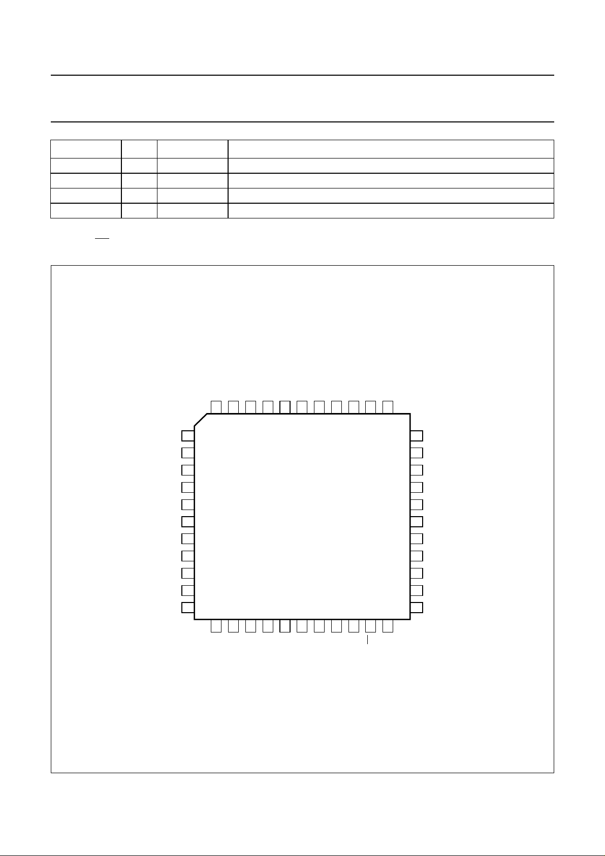
PINNING
SYMBOL PIN I/O DESCRIPTION
2
SCL 1 I serial clock input (I
NOSYNC 2 O not synchronized output (1 = not synchronized)
TRST 3 I boundary scan test reset (0 = active)
TCK 4 I boundary scan test clock
TMS 5 I boundary scan test mode select (1 = BST select)
TDI 6 I boundary scan test data input
TDO 7 O boundary scan test data output
V
SS
BCLK 9 O*
V
DD
BYTEO0 11 O*
BYTEO1 12 O*
BYTEO2 13 O*
V
SS
BYTEO3 15 O*
BYTEO4 16 O*
BYTEO5 17 O*
V
DD
BYTEO6 19 O*
BYTEO7 20 O*
8 − ground
(1)
byte clock output
10 − positive supply voltage
(1)
(1)
(1)
output data byte 0 (LSB)
output data byte 1
output data byte 2
14 − ground
(1)
(1)
(1)
output data byte 3
output data byte 4
output data byte 5
18 − positive supply voltage
(1)
(1)
output data byte 6
output data byte 7 (MSB)
OE 21 I output enable not (active LOW; 1 = O*
V
SS
BERR 23 O*
BEGIN 24 O*
V
DD
V
SS
22 − ground
(1)
(1)
block error output (1 = uncorrectable block)
begin of block output (1st byte of block is output)
25 − positive supply voltage
26 − ground
PORT5 27 I/O quasi-bidirectional port 5
PORT4 28 I/O quasi-bidirectional port 4
PORT3 29 I/O quasi-bidirectional port 3
PORT2 30 I/O quasi-bidirectional port 2
PORT1 31 I/O quasi-bidirectional port 1
PORT0 32 I/O quasi-bidirectional port 0
V
DD
33 − positive supply voltage
VALI 34 I valid input (1 = data is valid)
DATA1 35 I input data 1 (MSB)
DATA0 36 I input data 0 (LSB)
V
SS
37 − ground
CLK 38 I master clock input (also acting as input data clock)
V
DD
V
SS
39 − positive supply voltage
40 − ground
C-bus)
(1)
high impedance)
1996 Jul 17 4
Page 5
Philips Semiconductors Product specification
Reed Solomon decoder IC SAA7207H
SYMBOL PIN I/O DESCRIPTION
TC0 41 I test mode control input 0 (0 = application mode)
TC1 42 I test mode control input 1 (0 = application mode)
RESET 43 I master reset input (1 = active)
SDA 44 I/O bidirectional serial data port (I
Note
1. When OE is active (pin 21 = HIGH), all O* outputs become high impedance.
2
C-bus)
handbook, full pagewidth
SCL
NOSYNC
TRST
TCK
TMS
TDI
TDO
V
SS
BCLK
V
DD
BYTEO0
CLK
38
18
DD
V
SS
DATA0
V
37
36
19
20
BYTEO6
BYTEO7
DATA1
35
21
OE
VALI
34
22
SS
V
33
32
31
30
29
28
27
26
25
24
23
MBH314
V
DD
PORT0
PORT1
PORT2
PORT3
PORT4
PORT5
V
SS
V
DD
BEGIN
BERR
SDA
44
43
42
41
1
2
3
4
5
6
7
8
9
10
11
12
13
14
15
SS
V
BYTEO1
BYTEO2
BYTEO3
V
V
40
39
SAA7207H
16
17
BYTEO4
BYTEO5
DD
SS
TC0
TC1
RESET
Fig.2 Pin configuration.
1996 Jul 17 5
Page 6

1996 Jul 17 6
FUNCTIONAL DESCRIPTION
Input interface (see Fig.3)
The received input data stream is a sequence which is interpreted as a stream of bytes. The bits are assumed to be non-byte aligned and sent in
MSB to LSB order. New data may be present at the input pins on each rising edge of the master clock input (CLK). Valid data is indicated by
VALI = HIGH. When VALI = LOW the data is not valid and will be neglected. There are no limitations imposed on valid/non-valid sequences.
The Quadrature Amplitude Modulation (QAM) of the input data is given in Table 1.
Table 1 Quadrature amplitude modulation; note 1
QUADRATURE AMPLITUDE MODULATION
(2)
Philips Semiconductors Product specification
Reed Solomon decoder IC SAA7207H
SLOT
256 QAM 64 QAM 32 QAM 16 QAM 4 QAM
DATA1 DATA0 VALI DATA1 DATA0 VALI DATA1 DATA0 VALI DATA1 DATA0 VALI DATA1 DATA0 VALI
0S
1S
2S
3S
4S
5S
6S
7S
[7] S
n-1
[5] S
n-1
[3] S
n-1
[1] S
n-1
[7] Sn[6] 1 Sn[5] Sn[4] 1 S
n
[5] Sn[4] 1 Sn[3] Sn[2] 1 Sn[3] Sn[2] 1 Sn[1] Sn[0] 1 X X 0
n
[3] Sn[2] 1 Sn[1] Sn[0] 1 Sn[1] Sn[0] 1 X X 0 X X 0
n
[1] Sn[0]1XX0XX0XX0XX0
n
[6]1S
n-1
[4]1S
n-1
[2]1S
n-1
[0]1XX0XX0XX0XX0
n-1
n-1
n-1
n-1
[5] S
[3] S
[1] S
[4]1S
n-1
[2]1S
n-1
[0]1XX0XX0XX0
n-1
Notes
1. X = don’t care.
2. The numbers given in parenthesis refer to the bit numbers.
[4] S
n-1
[2] S
n-1
[0] Sn[4] 1 Sn[3] Sn[2] 1 Sn[1] Sn[0] 1
n-1
[3]1S
n-1
[1]1S
n-1
n-1
n-1
[3] S
[1] S
[2] 1 S
n-1
[0] 1 X X 0
n-1
n-1
[1] S
[0] 1
n-1
Page 7

Philips Semiconductors Product specification
Reed Solomon decoder IC SAA7207H
Synchronization (see Fig.4)
The input stream is interpreted as a stream of bytes
consisting of blocks which;
• Have a fixed 204 byte length
• Start with 1 synchronization byte.
Both de-interleaving and Reed Solomon decoding are
based on this block structure. Energy dispersal
descrambling is based on frames consisting of 8 blocks.
The first block of a frame has a sync byte of B8H, and the
remaining 7 blocks have a sync byte of 47H.
Consequently, there are 2 synchronization processes:
1. Synchronization process 1: handles byte alignment
and block synchronization. It is based on a state
machine running from state 0 (out of sync) to state 6
(fully synchronized).
2. Synchronization process 2: handles frame
synchronization for de-scrambling. It is based on the
detection of a B8H sync byte (after Reed Solomon
correction). Whenever such a sync byte is detected at
the beginning of a correct/corrected block, a free
running ‘block of frame counter’ is
synchronized/resynchronized.
With reference to note 2 in Fig 4, BERR is asserted at the
beginning of each new RS word (rising edge of BEGIN).
NOSYNC = 0 when 6 consecutive sync bytes have been
detected. BERR = 0 when the beginning of a frame has
been detected (de-scrambler lock) and not more than
8 bytes were wrong. When more than 8 bytes are wrong,
the BERR stays at logic 1 during the length of the word.
De-interleaving (see Fig.5)
Each of the units is dedicated to one of the following
decoder algorithm stages;
1. Power sum polynomial (syndrome) calculation
2. Execution of the Euclidean algorithm to find the error
locator polynomial and the error evaluator polynomial
3. Execution of a Chien search to find the roots of the
error locator polynomial. For each root the error value
is calculated (Forney algorithm) and stored in memory.
Code generator polynomial:
g (X) = (X + L0), (X + L1), (X + L2) to (X + L15)
where L = 02H
Field generator polynomial:
pX() X8 X4 X3 X2 1++++=
Error correction
The error correction unit corrects the errors as calculated
by the Reed Solomon unit if, and only if, they are
correctable. If not, the block is sent to the output
unmodified (i.e. as received). If ‘Transport Error Indicator’
(TEI = first bit after sync byte) modification is enabled the
error flag is set in all uncorrectable blocks.
In all cases the 16 parity bytes are stripped (the output is
set to zero; BCLK is stopped) from the block reducing it to
188 bytes length.
De-randomizing
The energy dispersal descrambling algorithm is based on
a 15 bit shift register which is initialised upon the arrival of
the Least Significant Bit (LSB) of the first byte of each
frame. De-scrambling is disabled for all sync bytes.
Input data is interleaved, conforming a convolutional
interleaving scheme. If we describe a Reed Solomon block
as a 0 to 203 one dimensional byte array then;
• Interleaving means that byte N of each block
(N=0to203) has been delayed by exactly D1 blocks
(D1 = N mod 12)
• So to de-interleave byte N of each block (N=0to203)
has to be delayed by D2 blocks [D2 = (203-N) mod 12].
Reed Solomon decoder
The IC contains a high throughput Reed Solomon decoder
consisting of three fully pipelined hardware units that
execute finite field computations on de-interleaved input
data blocks with lengths of 204 bytes.
1996 Jul 17 7
Output interface (see Fig.6)
The output data stream consists of a sequence of bytes
(BYTEO 7 is the MSB). A new byte is present at the output
pins at each rising edge of the byte clock. The BEGIN
output is asserted for the first byte of a block and negated
elsewhere. The BERR output is asserted during
uncorrectable and/or unsynchronized blocks and negated
during correct/corrected blocks.
Page 8

Philips Semiconductors Product specification
Reed Solomon decoder IC SAA7207H
Mode of operation
Table 2 Mode of operation for boundary scan test
PIN INTERNAL CONNECTION
APPLICATION MODE
(REED SOLOMON)
BOUNDARY SCAN TEST
TC0 pull-down logic 0 or open-circuit logic 0 or open-circuit
TC1 pull-down logic 0 or open-circuit logic 0 or open-circuit
TRST pull-up logic 0
(1)
logic 1 or open-circuit
TMS pull-up open-circuit input
TCK none open-circuit input
TDI pull-up open-circuit input
Note
1. The safest way to deactivate the Boundary Scan Test (BST) circuitry is to set TRST to logic 0.
Control, monitoring and extension port interface
An I2C-bus slave transmitter interface is included to provide the possibilities for a host to send control data and/or read
monitoring information. For details of the interface protocol and timing on the I2C-bus see
it”
; 12NC number 9398 393 40011.
“The I2C-bus and how to use
Table 3 Slave address
A6 A5 A4 A3 A2 A1 A0 R/
1101001X
W
(1)
Note
1. When X = 1 = read; whenX=0=write.
Table 4 Write (R/
BYTE LOGIC LEVEL DESCRIPTION
W=0)
(1)
1st byte 0 0 output data Port 5 to Port 0
2nd byte
(2)
ERF
(3)
0 mode control Port 5 to Port 0
Notes
1. Output data bits for port 5 to port 0; mode control bits for Port 5 to Port 0 (1 = input, 0 = output).
2. Sending the 2nd byte will force the IC to reset.
3. When ERF = 1 the error flag is set for uncorrectable blocks; when ERF = 0 the error flag is always left unmodified;
default: ERF = 1, mode control = 111111 (default = default value after a hardware reset).
1996 Jul 17 8
Page 9

Philips Semiconductors Product specification
Reed Solomon decoder IC SAA7207H
Table 5 Read (R/W=1)
BYTE LOGIC LEVEL DESCRIPTION
1st byte 0 0 input data Port 5 to Port 0
2nd byte S
(2)
− bits 22 to 16 of CorrCount
3rd byte −− bits 15 to 8 of CorrCount
4th byte −− bits 7 to 0 of CorrCount
Notes
1. Input data bits for Port 5 to Port 0.
2. When S = 0 it is in sync status; when S = 1 it is in no sync status.
The CorrCount is an estimation for the Byte Error Rate (BER) of the channel. This estimation is good for a high
signal-to-noise ratio (SNR); then all uncorrected blocks will not have more than 9 errors. The CorrCount is incremented
by 1 for each corrected byte. Each uncorrectable or unsychronized block will increment the CorrCount by 9. The
CorrCount will saturate at ‘7FFFFFH’ so that value actually means ‘counter overflow’.
A CorrCount reset is caused by the following:
• A hardware or software reset
• Reading the 4th byte.
(1)
ook, full pagewidth
CLK
DATA1
DATA0
VALI
SLOT 0
T
symbol
SLOT 1 SLOT 2 SLOT 3 SLOT 4
MBH318
Fig.3 Input Interface.
1996 Jul 17 9
Page 10

Philips Semiconductors Product specification
Reed Solomon decoder IC SAA7207H
handbook, full pagewidth
BEGIN (= sync)
NOSYNC
BERR
(1) De-interleaver lock (sync process 1).
(2) Descrambling lock (sync process 2) and the condition that not more than 8 byte errors have occurred.
(1)
Fig.4 Synchronization timing.
andbook, full pagewidth
0
17 x 11 single byte route
(2)
MBH316
0
1
9
10
11
17 x 10
Fig.5 De-interleaver (I = 12).
1996 Jul 17 10
17 x 2
17 = M
1
9
10
11 = I - 1
MBH317
Page 11

Philips Semiconductors Product specification
Reed Solomon decoder IC SAA7207H
handbook, full pagewidth
BEGIN
BCLK
BERR
sync
1 transport packet (188 bytes)
byte 2BYTEO (7 to 0)
1 RS word (204 bytes)
Fig.6 Output Interface timing.
LIMITING VALUES
In accordance with the Absolute Maximum Rating System (IEC 134).
RS (204, 188, 17)
byte 187 syncbyte 1
MBH326
SYMBOL PARAMETER MIN. MAX. UNIT
V
DD
V
i
I
i
I
o
T
stg
T
amb
supply voltage −0.3 +6.0 V
input voltage 0 V
DD
V
input current −10 +10 mA
output current −20 +20 mA
storage temperature −55 +150 °C
operating ambient temperature 0 70 °C
HANDLING
Inputs and outputs are protected against electrostatic discharges in normal handling. However, to be totally safe, it is
desirable to take normal precautions appropriate to handling integrated circuits.
Every pin withstands the ESD test in accordance with MIL-STD-883C category B (2000 V). Every pin withstands the ESD
test in accordance with Philips Semiconductors Machine Model; 0 Ω, 200 pF (200 V)
THERMAL CHARACTERISTICS
SYMBOL PARAMETER VALUE UNIT
R
thj-a
thermal resistance from junction to ambient in free air 61 K/W
1996 Jul 17 11
Page 12

Philips Semiconductors Product specification
Reed Solomon decoder IC SAA7207H
CHARACTERISTICS
=5V; T
V
DD
SYMBOL PARAMETER CONDITIONS MIN. TYP. MAX. UNIT
Digital inputs: pins 35, 36 and 34 (DATA1, DATA0 and VALI); see Fig.7
V
IL
V
IH
t
r
t
f
t
SU;DAT
t
HD;DAT
C
Ii
Digital outputs: pins 11 to 13, 15 to 17, 19, 20, 24 and 23 (BYTEO0 to BYTEO7, BEGIN and BERR); see Fig.8
V
OL
V
OH
t
d
t
HD;DAT
C
L
Clock input: pin 38 (CLK)
t
CLK
t
w
t
r
t
f
Clock output: pin 9 (BCLK)
t
BCLK
t
ow(BCLK)
=25°C; see notes 1 and 2; unless otherwise specified.
amb
LOW level input voltage −−0.8 V
HIGH level input voltage 2.0 −− V
rise time −−5ns
fall time −−5ns
set-up time 7 −− ns
hold time 5 −− ns
input capacitance − 5 − pF
LOW level output voltage 0 − 0.1V
HIGH level output voltage 0.9V
delay time CL=30pF 2T
hold time CL=30pF 2T
CLK
CLK
DD
− V
DD
− 30 −− ns
− 30 −− ns
DD
V
V
load capacitance −−30 pF
cycle time − 31.5 − ns
pulse width 40 : 60 duty 12 − 19 ns
rise time −−5ns
fall time −−5ns
BCLK cycle time 4T
BCLK pulse width 2T
CLK
CLK
−− ns
− 15 − 2T
+15 ns
CLK
Notes
1. Detailed timing of the RESET, NOSYNC, Port 0 to Port 5 and test pins is assumed not to be relevant for the
application.
2. For a proper RESET procedure the RESET pin should be HIGH during at least 5 rising edges of the CLK pin.
1996 Jul 17 12
Page 13

Philips Semiconductors Product specification
Reed Solomon decoder IC SAA7207H
handbook, full pagewidth
CLK
DATA0
DATA1
VALI
T
t
f
CLK
t
W
90%
10%
MBH319
t
r
t
SU;DAT
t
r
t
t
HD;DAT
f
Fig.7 Input data timing waveforms.
handbook, full pagewidth
BCLK
BYTEO (7 to 0)
BEGIN
BERR
t
HD;DAT
t
r
t
oW
t
d
Fig.8 Output data timing waveforms.
1996 Jul 17 13
T
BCLK
t
f
90%
10%
MBH320
Page 14

Philips Semiconductors Product specification
Reed Solomon decoder IC SAA7207H
handbook, full pagewidth
SDA
SCL
TDA8046
dout (1..0)
CLK
C
SDV
OUT
SAA7207H
DATA1
DATA0
valid
clk
VALI
CLK
Fig.9 Application diagram.
BYTEO
(7 to 0)
BERR
BEGIN
BCLK
d (7..0)d (1..0)
pkt_bad
pkt_sync
clk
SAA7205/06
M_in (7..0)
M_bad
M_sync
M_byte_clk
MBH321
1996 Jul 17 14
Page 15

Philips Semiconductors Product specification
Reed Solomon decoder IC SAA7207H
PACKAGE OUTLINE
QFP44: plastic quad flat package; 44 leads (lead length 1.3 mm); body 10 x 10 x 1.75 mm
c
y
X
A
33 23
34
pin 1 index
44
1
22
Z
E
e
H
E
E
w M
b
p
12
11
A
2
A
A
1
detail X
SOT307-2
Q
(A )
3
θ
L
p
L
w M
b
e
DIMENSIONS (mm are the original dimensions)
mm
OUTLINE
VERSION
SOT307-2
A
max.
2.10
0.25
0.05
1.85
1.65
UNIT A1A2A3b
Note
1. Plastic or metal protrusions of 0.25 mm maximum per side are not included.
p
D
H
D
cE
p
0.40
0.20
0.25
0.14
0.25
IEC JEDEC EIAJ
Z
D
B
0 2.5 5 mm
scale
(1)
(1) (1)(1)
D
10.1
9.9
REFERENCES
eH
10.1
9.9
12.9
0.8 1.3
12.3
1996 Jul 17 15
v M
H
v M
D
A
B
LLpQZywv θ
E
12.9
12.3
0.95
0.55
0.85
0.75
0.15 0.10.15
EUROPEAN
PROJECTION
Z
D
1.2
1.2
0.8
0.8
ISSUE DATE
92-11-17
95-02-04
E
o
10
o
0
Page 16

Philips Semiconductors Product specification
Reed Solomon decoder IC SAA7207H
SOLDERING
Introduction
There is no soldering method that is ideal for all IC
packages. Wave soldering is often preferred when
through-hole and surface mounted components are mixed
on one printed-circuit board. However, wave soldering is
not always suitable for surface mounted ICs, or for
printed-circuits with high population densities. In these
situations reflow soldering is often used.
This text gives a very brief insight to a complex technology.
A more in-depth account of soldering ICs can be found in
“IC Package Databook”
our
Reflow soldering
Reflow soldering techniques are suitable for all QFP
packages.
The choice of heating method may be influenced by larger
plastic QFP packages (44 leads, or more). If infrared or
vapour phase heating is used and the large packages are
not absolutely dry (less than 0.1% moisture content by
weight), vaporization of the small amount of moisture in
them can cause cracking of the plastic body. For more
information, refer to the Drypack chapter in our
Reference Handbook”
Reflow soldering requires solder paste (a suspension of
fine solder particles, flux and binding agent) to be applied
to the printed-circuit board by screen printing, stencilling or
pressure-syringe dispensing before package placement.
Several techniques exist for reflowing; for example,
thermal conduction by heated belt. Dwell times vary
between 50 and 300 seconds depending on heating
method. Typical reflow temperatures range from
215 to 250 °C.
Preheating is necessary to dry the paste and evaporate
the binding agent. Preheating duration: 45 minutes at
45 °C.
(order code 9398 652 90011).
“Quality
(order code 9398 510 63011).
Wave soldering
Wave soldering is not recommended for QFP packages.
This is because of the likelihood of solder bridging due to
closely-spaced leads and the possibility of incomplete
solder penetration in multi-lead devices.
If wave soldering cannot be avoided, the following
conditions must be observed:
• A double-wave (a turbulent wave with high upward
pressure followed by a smooth laminar wave)
soldering technique should be used.
• The footprint must be at an angle of 45° to the board
direction and must incorporate solder thieves
downstream and at the side corners.
Even with these conditions, do not consider wave
soldering the following packages: QFP52 (SOT379-1),
QFP100 (SOT317-1), QFP100 (SOT317-2),
QFP100 (SOT382-1) or QFP160 (SOT322-1).
During placement and before soldering, the package must
be fixed with a droplet of adhesive. The adhesive can be
applied by screen printing, pin transfer or syringe
dispensing. The package can be soldered after the
adhesive is cured.
Maximum permissible solder temperature is 260 °C, and
maximum duration of package immersion in solder is
10 seconds, if cooled to less than 150 °C within
6 seconds. Typical dwell time is 4 seconds at 250 °C.
A mildly-activated flux will eliminate the need for removal
of corrosive residues in most applications.
Repairing soldered joints
Fix the component by first soldering two diagonallyopposite end leads. Use only a low voltage soldering iron
(less than 24 V) applied to the flat part of the lead. Contact
time must be limited to 10 seconds at up to 300 °C. When
using a dedicated tool, all other leads can be soldered in
one operation within 2 to 5 seconds between
270 and 320 °C.
1996 Jul 17 16
Page 17

Philips Semiconductors Product specification
Reed Solomon decoder IC SAA7207H
DEFINITIONS
Data sheet status
Objective specification This data sheet contains target or goal specifications for product development.
Preliminary specification This data sheet contains preliminary data; supplementary data may be published later.
Product specification This data sheet contains final product specifications.
Limiting values
Limiting values given are in accordance with the Absolute Maximum Rating System (IEC 134). Stress above one or
more of the limiting values may cause permanent damage to the device. These are stress ratings only and operation
of the device at these or at any other conditions above those given in the Characteristics sections of the specification
is not implied. Exposure to limiting values for extended periods may affect device reliability.
Application information
Where application information is given, it is advisory and does not form part of the specification.
LIFE SUPPORT APPLICATIONS
These products are not designed for use in life support appliances, devices, or systems where malfunction of these
products can reasonably be expected to result in personal injury. Philips customers using or selling these products for
use in such applications do so at their own risk and agree to fully indemnify Philips for any damages resulting from such
improper use or sale.
2
PURCHASE OF PHILIPS I
C COMPONENTS
2
Purchase of Philips I
components in the I2C system provided the system conforms to the I2C specification defined by
Philips. This specification can be ordered using the code 9398 393 40011.
C components conveys a license under the Philips’ I2C patent to use the
1996 Jul 17 17
Page 18

Philips Semiconductors Product specification
Reed Solomon decoder IC SAA7207H
NOTES
1996 Jul 17 18
Page 19

Philips Semiconductors Product specification
Reed Solomon decoder IC SAA7207H
NOTES
1996 Jul 17 19
Page 20

Philips Semiconductors – a worldwide company
Argentina: see South America
Australia: 34 Waterloo Road, NORTH RYDE, NSW 2113,
Tel. +61 2 9805 4455, Fax. +61 2 9805 4466
Austria: Computerstr. 6, A-1101 WIEN, P.O. Box 213,
Tel. +43 1 60 101, Fax. +43 1 60 101 1210
Belarus: Hotel Minsk Business Center, Bld. 3, r. 1211, Volodarski Str. 6,
220050 MINSK, Tel. +375 172 200 733, Fax. +375 172 200 773
Belgium: see The Netherlands
Brazil: see South America
Bulgaria: Philips Bulgaria Ltd., Energoproject, 15th floor,
51 James Bourchier Blvd., 1407 SOFIA,
Tel. +359 2 689 211, Fax. +359 2 689 102
Canada: PHILIPS SEMICONDUCTORS/COMPONENTS,
Tel. +1 800 234 7381, Fax. +1 708 296 8556
China/Hong Kong: 501 Hong Kong Industrial Technology Centre,
72 Tat Chee Avenue, Kowloon Tong, HONG KONG,
Tel. +852 2319 7888, Fax. +852 2319 7700
Colombia: see South America
Czech Republic: see Austria
Denmark: Prags Boulevard 80, PB 1919, DK-2300 COPENHAGEN S,
Tel. +45 32 88 2636, Fax. +45 31 57 1949
Finland: Sinikalliontie 3, FIN-02630 ESPOO,
Tel. +358 615 800, Fax. +358 615 80920
France: 4 Rue du Port-aux-Vins, BP317, 92156 SURESNES Cedex,
Tel. +33 1 40 99 6161, Fax. +33 1 40 99 6427
Germany: Hammerbrookstraße 69, D-20097 HAMBURG,
Tel. +49 40 23 52 60, Fax. +49 40 23 536 300
Greece: No. 15, 25th March Street, GR 17778 TAVROS,
Tel. +30 1 4894 339/911, Fax. +30 1 4814 240
Hungary: see Austria
India: Philips INDIA Ltd, Shivsagar Estate, A Block, Dr. Annie Besant Rd.
Worli, MUMBAI 400 018, Tel. +91 22 4938 541, Fax. +91 22 4938 722
Indonesia: see Singapore
Ireland: Newstead, Clonskeagh, DUBLIN 14,
Tel. +353 1 7640 000, Fax. +353 1 7640 200
Israel: RAPAC Electronics, 7 Kehilat Saloniki St, TEL AVIV 61180,
Tel. +972 3 645 0444, Fax. +972 3 648 1007
Italy: PHILIPS SEMICONDUCTORS, Piazza IV Novembre 3,
20124 MILANO, Tel. +39 2 6752 2531, Fax. +39 2 6752 2557
Japan: Philips Bldg 13-37, Kohnan 2-chome, Minato-ku, TOKYO 108,
Tel. +81 3 3740 5130, Fax. +81 3 3740 5077
Korea: Philips House, 260-199 Itaewon-dong, Yongsan-ku, SEOUL,
Tel. +82 2 709 1412, Fax. +82 2 709 1415
Malaysia: No. 76 Jalan Universiti, 46200 PETALING JAYA, SELANGOR,
Tel. +60 3 750 5214, Fax. +60 3 757 4880
Mexico: 5900 Gateway East, Suite 200, EL PASO, TEXAS 79905,
Tel. +1 800 234 7381, Fax. +1 708 296 8556
Middle East: see Italy
Netherlands: Postbus 90050, 5600 PB EINDHOVEN, Bldg. VB,
Tel. +31 40 27 83749, Fax. +31 40 27 88399
New Zealand: 2 Wagener Place, C.P.O. Box 1041, AUCKLAND,
Tel. +64 9 849 4160, Fax. +64 9 849 7811
Norway: Box 1, Manglerud 0612, OSLO,
Tel. +47 22 74 8000, Fax. +47 22 74 8341
Philippines: Philips Semiconductors Philippines Inc.,
106 Valero St. Salcedo Village, P.O. Box 2108 MCC, MAKATI,
Metro MANILA, Tel. +63 2 816 6380, Fax. +63 2 817 3474
Poland: Ul. Lukiska 10, PL 04-123 WARSZAWA,
Tel. +48 22 612 2831, Fax. +48 22 612 2327
Portugal: see Spain
Romania: see Italy
Russia: Philips Russia, Ul. Usatcheva 35A, 119048 MOSCOW,
Tel. +7 095 926 5361, Fax. +7 095 564 8323
Singapore: Lorong 1, Toa Payoh, SINGAPORE 1231,
Tel. +65 350 2538, Fax. +65 251 6500
Slovakia: see Austria
Slovenia: see Italy
South Africa: S.A. PHILIPS Pty Ltd., 195-215 Main Road Martindale,
2092 JOHANNESBURG, P.O. Box 7430 Johannesburg 2000,
Tel. +27 11 470 5911, Fax. +27 11 470 5494
South America: Rua do Rocio 220, 5th floor, Suite 51,
04552-903 São Paulo, SÃO PAULO - SP, Brazil,
Tel. +55 11 821 2333, Fax. +55 11 829 1849
Spain: Balmes 22, 08007 BARCELONA,
Tel. +34 3 301 6312, Fax. +34 3 301 4107
Sweden: Kottbygatan 7, Akalla, S-16485 STOCKHOLM,
Tel. +46 8 632 2000, Fax. +46 8 632 2745
Switzerland: Allmendstrasse 140, CH-8027 ZÜRICH,
Tel. +41 1 488 2686, Fax. +41 1 481 7730
Taiwan: PHILIPS TAIWAN Ltd., 23-30F, 66,
Chung Hsiao West Road, Sec. 1, P.O. Box 22978,
TAIPEI 100, Tel. +886 2 382 4443, Fax. +886 2 382 4444
Thailand: PHILIPS ELECTRONICS (THAILAND) Ltd.,
209/2 Sanpavuth-Bangna Road Prakanong, BANGKOK 10260,
Tel. +66 2 745 4090, Fax. +66 2 398 0793
Turkey: Talatpasa Cad. No. 5, 80640 GÜLTEPE/ISTANBUL,
Tel. +90 212 279 2770, Fax. +90 212 282 6707
Ukraine: PHILIPS UKRAINE, 2A Akademika Koroleva str., Office 165,
252148 KIEV, Tel. +380 44 476 0297/1642, Fax. +380 44 476 6991
United Kingdom: Philips Semiconductors Ltd., 276 Bath Road, Hayes,
MIDDLESEX UB3 5BX, Tel. +44 181 730 5000, Fax. +44 181 754 8421
United States: 811 East Arques Avenue, SUNNYVALE, CA 94088-3409,
Tel. +1 800 234 7381, Fax. +1 708 296 8556
Uruguay: see South America
Vietnam: see Singapore
Yugoslavia: PHILIPS, Trg N. Pasica 5/v, 11000 BEOGRAD,
Tel. +381 11 825 344, Fax.+381 11 635 777
For all other countries apply to: Philips Semiconductors, Marketing & Sales Communications,
Building BE-p, P.O. Box 218, 5600 MD EINDHOVEN, The Netherlands, Fax. +31 40 27 24825
© Philips Electronics N.V. 1996 SCA50
All rights are reserved. Reproduction in whole or in part is prohibited without the prior written consent of the copyright owner.
The information presented in this document does not form part of any quotation or contract, is believed to be accurate and reliable and may be changed
without notice. No liability will be accepted by the publisher for any consequence of its use. Publication thereof does not convey nor imply any license
under patent- or other industrial or intellectual property rights.
Printed in The Netherlands 537021/1200/01/pp20 Date of release: 1996 Jul 17 Document order number: 9397 750 00964
Internet: http://www.semiconductors.philips.com/ps/
(1) SAA7207H_1.copy June 26, 1996 11:51 am
 Loading...