

Page 1

INTEGRATED CIRCUITS
DATA SH EET
SAA7206H
DVB compliant descrambler
Product specification
Supersedes data of 1996 Oct 02
File under Integrated Circuits, IC02
1996 Oct 09
Page 2

Philips Semiconductors Product specification
DVB compliant descrambler SAA7206H
CONTENTS
1 FEATURES
2 GENERAL DESCRIPTION
3 ORDERING INFORMATION
4 QUICK REFERENCE DATA
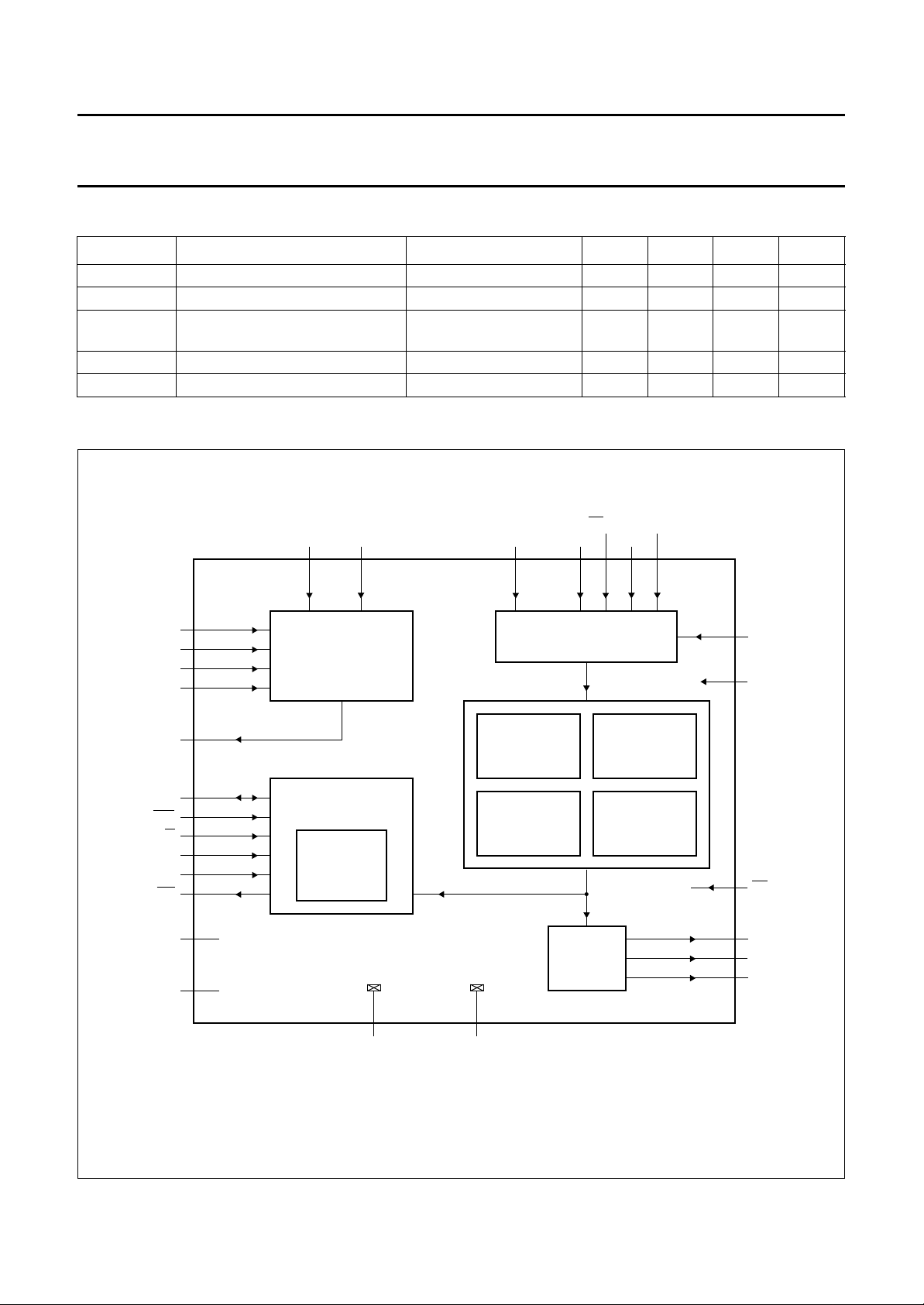
5 BLOCK DIAGRAM
6 PINNING
7 FUNCTIONAL DESCRIPTION
7.1 MPEG-2 systems parsing
7.2 PES level descrambling
7.3 Descrambler core
7.4 Microcontroller interface
7.5 Output interfacing
7.6 Boundary scan test
7.7 Programming the descrambler
8 LIMITING VALUES
9 HANDLING
10 THERMAL CHARACTERISTICS
11 DC CHARACTERISTICS
12 AC CHARACTERISTICS
13 PACKAGE OUTLINE
14 SOLDERING
14.1 Introduction
14.2 Reflow soldering
14.3 Wave soldering
14.3.1 QFP
14.3.2 SO
14.3.3 Method (QFP and SO)
14.4 Repairing soldered joints
15 DEFINITIONS
16 LIFE SUPPORT APPLICATIONS
1996 Oct 09 2
Page 3

Philips Semiconductors Product specification
DVB compliant descrambler SAA7206H
1 FEATURES
• Input data fully compliant with the Transport Stream
(TS) definition of the MPEG-2 systems specification
• Input data signals; [Forward Error Correction (FEC)
Interface]
– modem data input bus (8-bit wide)
– valid input data indicator
– erroneous packet indicator
– first packet byte indicator
– byte strobe signal (for asynchronous mode only).
The interface can be programmed to one of two modes:
– Asynchronous mode; byte strobe input signal
(MBCLK) < 9 MHz, for connection to a modem (FEC)
– Synchronous mode; MBCLK is not used. Data is
delivered to the descrambler synchronized with the
chip clock (DCLK) [9 MHz (typ.) with a 33% duty
cycle].
• No external memory
• Effective bit rate; f
• Control interface; 8-bit multiplexed data/address,
memory mapped I/O (90CE201 microcontroller parallel
bus compatible), in combination with a microcontroller
interrupt signal (IRQ)
• Output ports are identical to the input data interface
(demultiplexer interface)
– except for the packet error indicator (MB/MB), as the
descrambler translates an active MB signal to the
‘transport_error_indicator’ bit in the transport stream
– except for the byte strobe input signal (MBCLK), as
data is delivered to the demultiplexer, synchronized
with the descrambler chip clock which is generated
by the demultiplexer
≤ 72 MHz
bit
• Descrambler, based on the super descrambler
mechanism algorithm with stream decipher and block
decipher. The descrambler is initialized with a 64-bit
Control Word (CW) at the beginning of a transport
stream packet payload of a selected Packet
Identification (PID). The descrambler operates on
transport stream packet or Packetized Elementary
Stream (PES) packet payloads
• Microcontroller support; only for control, no specific
descrambling tasks are performed by the
microcontroller. However, parsing and processing of
conditional access information (such as EMM and ECM
data) is left to the system microcontroller
• Boundary scan test port for boundary scan.
2 GENERAL DESCRIPTION
The SAA7206H (DVB compliant) is designed for use in
MPEG-2 based digital TV receivers, incorporating
conditional access filters. Such receivers are to be
implemented in, for instance, a digital video broadcasting
top set box, or an integrated digital TV receiver.
An example of a demultiplexer/descrambler system
configuration, containing a channel decoder module, a
demultiplexer, a system controller and a conditional
access system is shown in Fig.3. The main function of the
descrambler is to descramble the payloads of MPEG-2 TS
packets or PES packets. In addition, the descrambler
retrieves Conditional Access (CA) data [such as
Entitlement Management Messages (EMM) and
Entitlement Control Messages (ECM) etc.] from the stream
and passes it to the system microcontroller for processing.
3 ORDERING INFORMATION
PACKAGE
TYPE NUMBER
NAME DESCRIPTION VERSION
SAA7206H QFP64 plastic quad flat package; 64 leads (lead length 1.95 mm);
body 14 × 20 × 2.8 mm
1996 Oct 09 3
SOT319-2
Page 4
Philips Semiconductors Product specification
DVB compliant descrambler SAA7206H
4 QUICK REFERENCE DATA
SYMBOL PARAMETER CONDITIONS MIN. TYP. MAX. UNIT
V
DDD
V
DDD(core)
P
tot
f
clk
T
amb
5 BLOCK DIAGRAM
digital supply voltage −−5.5 V
digital supply voltage for core −−3.6 V
total power dissipation V
DDD(core)
V
DDD
= 3.3 V,
=5V, CL=15pF
−−250 mW
clock frequency duty cycle = 30 to 55% −−9 MHz
operating ambient temperature 0 − 70 °C
handbook, full pagewidth
TDI
TCK
TMS
TRST
TDO
DAT7
to
DAT0
DCS
R/W
A1
A0
IRQ
V
DDD(core)
V
DDD1
to
V
DDD9
18
19
20
46
37
7 to 9,
12 to 16
3
63
4
5
1
36
6, 11, 21, 26,
32, 41, 51, 57, 64
TC1 TC0
61 60
TEST CONTROL BLOCK
BOUNDARY SCAN TEST
FOR
AND
SCAN TEST
SAA7206
MICROCONTROLLER
INTERFACE
CONDITIONAL
ACCESS
FILTERS
2, 17, 23, 27,
33, 52, 58
V
to V
SSD1
SSD7
V
SSD1(core)
V
SSD2(core)
MIN7 to MIN0
47 to 50,
53 to 56
TRANSPORT STREAMS
PACKET
IDENTIFICATION
BANK
STREAM
DECIPHER
10, 42
,
MB/MB
MDV
44 45 43 59
AND
AF PARSER
OUTPUT
INTERFACE
MBCLK
MSYNC
CONTROL
WORD
BANK
BLOCK
DECIPHER
24, 25,
28 to 31,
34, 35
MGG313
22
DCLK
62
POR
40
OE
DATO0
to
DATO7
38
DVO
39
SYNCO
Fig.1 Block diagram.
1996 Oct 09 4
Page 5

Philips Semiconductors Product specification
DVB compliant descrambler SAA7206H
6 PINNING
SYMBOL PIN I/O DESCRIPTION
IRQ 1 O interrupt request output for microcontroller (active LOW, open-drain output)
V
SSD1
DCS 3 I descrambler chip select input (active LOW)
A1 4 I A1 = address/data indicator input
A0 5 I A0 = MSByte indicator input
V
DDD1
DAT7 7 I/O microcontroller bidirectional data bus bit 7
DAT6 8 I/O microcontroller bidirectional data bus bit 6
DAT5 9 I/O microcontroller bidirectional data bus bit 5
V
SSD1(core)
V
DDD2
DAT4 12 I/O microcontroller bidirectional data bus bit 4
DAT3 13 I/O microcontroller bidirectional data bus bit 3
DAT2 14 I/O microcontroller bidirectional data bus bit 2
DAT1 15 I/O microcontroller bidirectional data bus bit 1
DAT0 16 I/O microcontroller bidirectional data bus bit 0
V
SSD2
TDI 18 I boundary scan test data input
TCK 19 I boundary scan test clock input
TMS 20 I boundary scan test mode select input
V
DDD3
DCLK 22 I 9 MHz descrambler chip clock input (duty cycle range: 30 to 55%)
V
SSD3
DATO0 24 O data output to demultiplexer bit 0
DATO1 25 O data output to demultiplexer bit 1
V
DDD4
V
SSD4
DATO2 28 O data output to demultiplexer bit 2
DATO3 29 O data output to demultiplexer bit 3
DATO4 30 O data output to demultiplexer bit 4
DATO5 31 O data output to demultiplexer bit 5
V
DDD5
V
SSD5
DATO6 34 O data output to demultiplexer bit 6
DATO7 35 O data output to demultiplexer bit 7
V
DDD(core)
TDO 37 O boundary scan test data output
DVO 38 O valid output data indicator
SYNCO 39 O indicates the first output byte (sync) of a transport packet
2 GND digital ground 1
6 supply digital supply voltage 1 (+5 V)
10 GND digital ground 1 for core
11 supply digital supply voltage 2 (+5 V)
17 GND digital ground 2
21 supply digital supply voltage 3 (+5 V)
23 GND digital ground 3
26 supply digital supply voltage 4 (+5 V)
27 GND digital ground 4
32 supply digital supply voltage 5 (+5 V)
33 GND digital ground 5
36 supply digital supply voltage for core (+3.3 V)
1996 Oct 09 5
Page 6

Philips Semiconductors Product specification
DVB compliant descrambler SAA7206H
SYMBOL PIN I/O DESCRIPTION
OE 40 I output enable (active LOW), if HIGH, device outputs are high impedance,
(connected to logic 0 in normal operation)
V
DDD6
V
SSD2(core)
MSYNC 43 I indicates the first input byte (sync) of a transport packet
MDV 44 I valid input data indicator
MB/MB 45 I packet error indicator input (programmable polarity)
TRST 46 I boundary scan reset input (LOW in normal operation)
MIN7 47 I 8-bit wide modem data input bit 7
MIN6 48 I 8-bit wide modem data input bit 6
MIN5 49 I 8-bit wide modem data input bit 5
MIN4 50 I 8-bit wide modem data input bit 4
V
DDD7
V
SSD6
MIN3 53 I 8-bit wide modem data input bit 3
MIN2 54 I 8-bit wide modem data input bit 2
MIN1 55 I 8-bit wide modem data input bit 1
MIN0 56 I 8-bit wide modem data input bit 0
V
DDD8
V
SSD7
MBCLK 59 I byte strobe input signal < 9 MHz
TC0 60 I test control input 0 (not connected in normal operation)
TC1 61 I test control input 1 (not connected in normal operation)
POR 62 I power-on reset, must be active HIGH during at least 5 DCLK pulses
W 63 I read/write input selection
R/
V
DDD9
41 supply digital supply voltage 6 (+5 V)
42 GND digital ground 2 for core
51 supply digital supply voltage 7 (+5 V)
52 GND digital ground 6
57 supply digital supply voltage 8 (+5 V)
58 GND digital ground 7
64 supply digital supply voltage 9 (+5 V)
1996 Oct 09 6
Page 7

Philips Semiconductors Product specification
DVB compliant descrambler SAA7206H
handbook, full pagewidth
V
SSD1
V
DDD1
DAT7
DAT6
DAT5
V
SSD1(core)
V
DDD2
DAT4
DAT3
DAT2
DAT1
DAT0
V
SSD2
IRQ
DCS
A1
A0
TDI
TCK
DDD9
V
R/W
POR
TC1
TC0
64
63
62
61
60
1
2
3
4
5
6
7
8
9
10
11
12
13
14
15
16
17
18
19
20
21
22
23
24
TMS
DDD3
V
DCLK
SSD3
V
DATO0
SSD7VDDD8
MBCLK
V
59
58
SAA7206
25
26
DDD4
DATO1
V
57
27
SSD4
V
MIN0
56
28
DATO2
MIN1
55
29
DATO3
MIN2
54
30
DATO4
MIN3
V
53
31
DATO5
SSD6
52
32
DDD5
V
51
50
49
48
47
46
45
44
43
42
41
40
39
38
37
36
35
34
33
MGG312
V
DDD7
MIN4
MIN5
MIN6
MIN7
TRST
MB/MB
MDV
MSYNC
V
SSD2(core)
V
DDD6
OE
SYNCO
DVO
TDO
V
DDD(core)
DATO7
DATO6
V
SSD5
Fig.2 Pin configuration.
1996 Oct 09 7
Page 8

Philips Semiconductors Product specification
DVB compliant descrambler SAA7206H
7 FUNCTIONAL DESCRIPTION
A block diagram of the internal structure of the
descrambler (DVB compliant) is illustrated in Fig.1.
The block diagram illustrates the main functional modules
in the descrambler. The modules are as follows:
• The MPEG-2 syntax parser, which parses transport
streams that comply with the MPEG-2 systems
specification
• The descrambler module consisting of:
– A Packet Identification (PID) bank containing 6 PID
values of the streams selected for descrambling.
All bits of PID5 (address 0x0205) can be masked
individually with PID5_mask (address 0x0209), to
enable multiple PID selection.
– A Control Word (CW) bank containing 6 CW pairs
and a default CW. A CW pair consists of
2 descrambler control words (odd and even), each
word with a length of 64 bits.
– The descrambler core containing the actual
descrambler with the stream cipher and the block
cipher module.
• A microcontroller interface providing protocol handling
for the memory mapped I/O control bus
(Philips 90CE201 compatible). This module contains an
interrupt request handler and data filters for the retrieval
of Conditional Access (CA) information:
• The CA filters select data on the basis of PIDs, and a
combination of MPEG-2 section addressing fields.
Selected CA data is stored in eighteen 256 byte
(constrained random access) buffers which can be read
by the microcontroller. The CA message section has a
maximum length of 256 bytes. It consists of a 3 bytes
long header with Table_id and section_length data.
The remaining part of the CA message are the
CA_data_bytes (see Fig.4). If a section is longer than
256 bytes, the data capture is stopped (with an interrupt
to the microcontroller) after 256 bytes are in the buffer
and the ‘section_to_long’ bit is set. The filters are
capable of monitoring 18 CA streams (containing EMM
and ECM data) simultaneously. Two different lengths
are used for address filtering:
– 16 filters where the first 7 bytes of the CA_data_bytes
field are used for address filtering
– 2 (DVB compliant) filters where the first 17 bytes of
the CA_data_bytes field are used for address filtering
– A chip identification byte (value 0x02) can be read by
the software from address 0x0003 (see Table 10).
handbook, full pagewidth
CONDITIONAL
ACCESS
SYSTEM
DEMODULATOR
AND
FORWARD ERROR
CORRECTOR
MICRO-
CONTROLLER
DESCRAMBLER
(SAA7206H)
Fig.3 Demultiplexer system configuration.
1996 Oct 09 8
DVB
DEMULTIPLEXER
(SAA7205)
MGG314
Page 9
Philips Semiconductors Product specification
DVB compliant descrambler SAA7206H
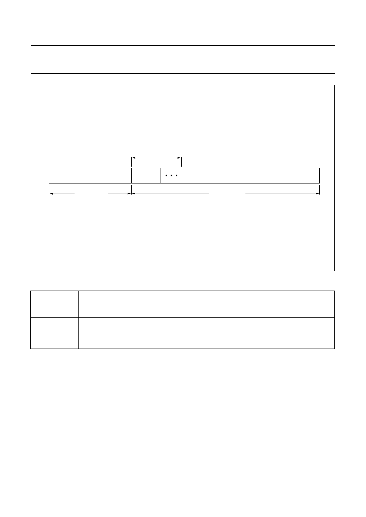
handbook, full pagewidth
table_id reserved section length byte 0 byte 1
section header
(3 bytes)
7 or 17 bytes
of filtering
CA_data_bytes
[253 bytes (max.)]
section payload
[253 bytes (max.)]
MGG316
Fig.4 Syntax of the conditional access message.
Table 1 Explanation of Fig.4
SYNTAX DESCRIPTION
Table_id 8-bit field for identification
Reserved 4-bit field with section_syntax_indicator (1 bit), DVB_reserved (1 bit) and ISO_reserved (2 bits)
Section_length 12-bit field that specifies the number of bytes that follow the section_length field up to the end of
the section
CA_data_byte 8-bit field that carries private CA information. Up to the first 17 CA_data_bytes may be used for
address filtering
1996 Oct 09 9
Page 10

Philips Semiconductors Product specification
DVB compliant descrambler SAA7206H
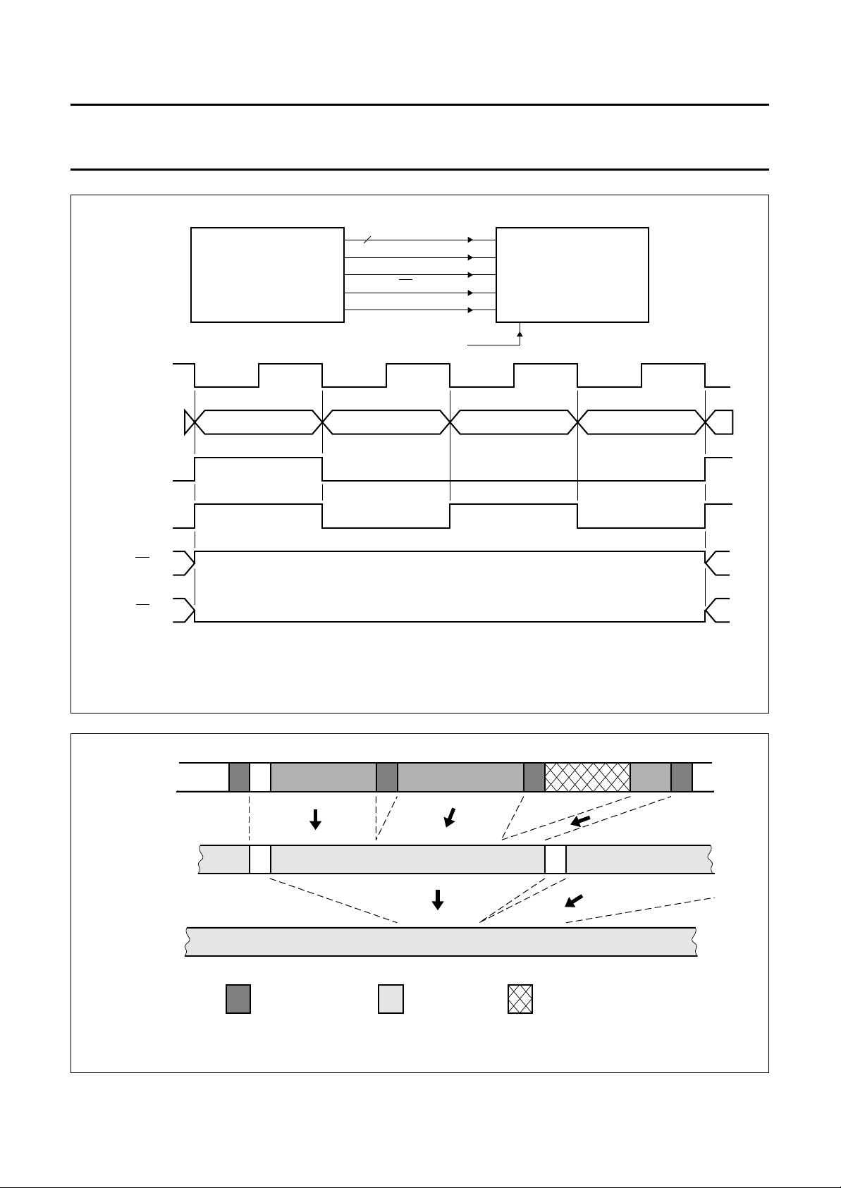
7.1 MPEG-2 systems parsing
The descrambler receives data from a Forward Error
Correction (FEC) decoder (see Fig.5) in a digital TV
receiver, in the following input data format:
• 8 data bits via MIN7 to MIN0.
• A valid input data indicator signal (MDV), which is HIGH
for consecutive valid bytes and output by either a FEC
decoder or a descrambler. Consequently the
descrambler input data is allowed to have a ‘bursty’
nature.
• A transport packet error indicator (
HIGH for the duration of each 188 byte transport packet
in which the FEC decoder found more errors than it
could correct. The polarity (active HIGH or LOW) of the
error indicator is programmable [bit ‘Bad_polarity’
(see Table 10, address 0x0100)].
• A packet sync signal (MSYNC) which goes HIGH at the
start of the first byte of a transport packet. Only the rising
edge of MSYNC is used for synchronization, the exact
HIGH time of the signal is therefore irrelevant.
• A byte strobe signal (MBCLK; < 9 MHz) which indicates
consecutive data bytes in the input stream, in the non
9 MHz mode only [bit ‘9 MHz_interface’ = 0
(see Table 10, address 0x0100)]. MBCLK is used as an
enable signal, and transport stream input bytes are
sampled on its rising edges. If the input interface is
programmed to the 9 MHz mode
(‘9 MHz_interface’ = 1), the MBCLK signal is ignored
and bytes are latched on rising edges of the DCLK.
• A descrambler clock signal (DCLK; 9 MHz; duty cycle
range 30 to 55%) which is the processing clock for the
descrambler IC. If rising edges of this signal are used to
input data to the descrambler, the 9 MHz mode must be
programmed (bit ‘9 MHz_interface’ = 1, see Table 10,
address 0x0100).
MB/MB) which is
The hierarchical multiplex level below the MPEG-2
transport stream is the packetized elementary stream.
The PES header is only parsed partially by the DVB
descrambler to locate its scrambling control bits. Parsing is
performed for all incoming transport packets, and the
parser is synchronized to a rising edge on its MSYNC
input. A microcontroller can compose a set of 6 PIDs by
programming the appropriate registers in the PID filter
bank within the descrambler.
These PIDs identify the packets of the streams that are to
be descrambled. All 13 bits of PID5 (see Table 10,
address 0x0205) can be individually enabled/disabled with
a mask of 13 bits (see Table 10, address 0x0209) to
enable multiple PID selection. The PIDs of PES scrambled
packets must be indicated by programming a logic 1 to the
corresponding bit of the ‘PIDi_is_pes’ word
(see Table 10, address 0x0206).
MPEG-2 multiplex fields which are related to CA
information, in so called sections, are parsed only partly.
CA sections containing for instance Entitlement
Management Messages (EMM) and Entitlement Control
Messages (ECM) etc. are retrieved from the stream and
stored in 256 byte buffers in the CA filter module. For the
selection of CA data, 18 additional PIDs and section
header information (table_id, address field, both with bit
masks) can be programmed. All 13 bits of PID filters
16 and 17 can be individually enabled/disabled with a
mask of 13 bits (see Table 10, addresses 0x03A6
and 0x03BA) to enable multiple PID selection for CA
messages. A microcontroller may access data in the
256 byte CA buffers (each filter has its own buffer thus
18 in total) for software based parsing and processing.
The parser module in the descrambler parses transport
streams compliant to the MPEG-2 systems syntax.
MPEG-2 systems specifies a hierarchical two-level
multiplex (see Fig.6). The top hierarchical level is the
transport stream, consisting of relatively short (188 byte)
transport packets. Each transport packet consists of a
4 byte transport header, an optional adaptation field and a
payload. The transport header contains a 13-bit PID field.
The adaptation field may contain Program Clock
Reference (PCR) data and transport private data, among
others. Both transport header and optional adaptation
fields are parsed by the TS parser module.
1996 Oct 09 10
Page 11
Philips Semiconductors Product specification
DVB compliant descrambler SAA7206H
8
handbook, full pagewidth
FEC
MBCLK
MIN7 to MIN0
MBCLK
MDV
MB/MB
MSYNC
DESCRAMBLER
DCLK
MIN7 to MIN0
MSYNC
MDV
MB/MB
MB/MB
handbook, full pagewidth
transport
stream
message invalid data
error-free transport packet (programmable polarity)
erroneous transport packet
message invalid data
Fig.5 Signal constellation FEC decoder - descrambler Interfacing.
MGG317
packetized
elementary
stream
elementary
stream
= transport_header = pes_header = stuffing
Fig.6 MPEG-2 two level hierarchical demultiplexing.
1996 Oct 09 11
MGG318
Page 12

Philips Semiconductors Product specification
DVB compliant descrambler SAA7206H
7.2 PES level descrambling
PES level descrambling is possible in accordance with the
recommendations of the DVB standard with the DVB
descrambler IC. The actual restrictions however, required
by the DVB descrambler IC, are less strict than to the
recommendations in the DVB standard. The restrictions
for PES level descrambling imposed by the IC are as
follows:
• Scrambling shall only occur at one level (TS or PES) and
is not allowed to occur at both levels simultaneously
• The complete PES header must be present in exactly
one TS packet. Consequently, the size of a PES packet
header shall not exceed 184 bytes
• Only the PES packet data bytes (PES payload) are
descrambled
• TS packets resulting from scrambling at PES level are
not chained and thus are independent. Consequently,
the internal descrambler algorithms (stream decipher
and block decipher) are initialized at the start of each
(PES scrambled) TS packet payload.
In order to be able to distinguish between sections and
PES packets, a PID for a PES scrambled packet is
indicated by programming the according ‘PIDi_is_pes’ bit
(see Table 10, address 0x0206) to logic 1. If the
payload_unit_start_indicator bit is set in the TS packet
header and the ‘PIDi_is_pes’ bit is set for a particular PID,
the PES scrambling control bits, which are present in the
PES header, are stored in the accessible ‘pes_sc_PIDi’
register (see Table 10, address 0x0208).
Descrambling at TS level always has priority over
descrambling at PES level. Consequently, PES level
descrambling is only possible when the
transport_scrambling_control bits in the TS header are
‘00’. In that situation the payload of the PES packets is
descrambled using the scrambling control bits of the
‘pes_sc_PIDi’ register.
Remark: PID masking (for PID5) should not be combined
with PES level descrambling. Only one pair of PES
scrambling control bits per PID is stored in an Internal
register. Thus interleaving of PES messages, which can
occur in the situation of multiple PID selection, can give the
wrong descrambling result. As a consequence the
microcontroller must program the ‘PID5_is_pes’ bit
(see Table 10, address 0x0206) to logic 0 when multiple
PID selection is used.
7.3 Descrambler core
The descrambler core consists of three modules:
• A PID filter which selects packets for descrambling
• A control word bank containing 6 sets (odd and even) of
control words and a Default Control Word (DCW)
• The super descrambler core with the implementation of
the stream decipherment and the block decipherment
algorithms.
The PID filter contains 6 registers which hold data in the
format indicated in Fig.7. Six individual PIDs are stored to
identify 6 packet streams. All bits of PID5 (see Table 10,
address 0x0205) can be masked with the ‘PID5_mask’
(see Table 10, address 0x209), to enable descrambling on
multiple PIDs. To disable a bit of PID5 with the
‘PID5_mask’ a logic 0 must be programmed. After a
power-on reset pulse all mask bits are preset to logic 1.
To each PID a 3-bit Control Word Pair Index pointer
(CWPI) is attached. A CWPI prescribes which control word
pair, consisting of odd and even control words, has to be
used to initialize the DVB descrambler for payloads of
packets with the associated PID. After a power-on reset all
CWPIs are set to ‘111’ to enable a correct initialization of
the conditional access system.
If two or more programmed PIDs match the PID of the TS
packet at the same time (while the CWPI value of the
programmed PIDs is not equal to ‘110’ or ‘111’), the
programmed PID with the lower index number has a higher
priority. However, the default control word, when enabled,
has the highest priority.
Thus, the built-in priority (HIGH-to-LOW transition) for the
programmed PIDs is; DCW, PID0, PID1, PID2, PID3, PID4
and PID5.
A 2-bit scrambling_control field is present in the TS packet
header and in the PES header (ts_sc1 and ts_sc0 and
pes_sc1 and pes_sc0 respectively). The bits in this
header field indicate whether the TS packet or PES
payload is scrambled or not. In addition, these bits also
indicate which control word (odd or even) of a control word
pair was used to initialize the DVB descrambler, as
indicated in Tables 2 and 3.
1996 Oct 09 12
Page 13

Philips Semiconductors Product specification
DVB compliant descrambler SAA7206H
If the payload of a packet is descrambled, the descrambler
subsequently resets the scrambling_control bits in the TS
or PES header (to ‘00’). For each of the 6 PIDs in the PID
filter bank the values of the TS scrambling_control bits are
stored in a microcontroller accessible register, prior to
descrambling [bits: ‘ts_sc_PIDi1’ and ‘ts_sc_PIDi0’;
(see Table 10, address 0x0208), ‘i’ is in the range 5 to 0].
For each of the 6 PIDs in the PID filter bank, of which the
corresponding PIDi_is_pes bit (see Table 10,
address 0x0206) is also set to logic 1, the values of the
PES scrambling_control bits are stored in a
microcontroller accessible register, prior to descrambling
[bits:‘pes_sc_PIDi1’ and ‘pes_sc_PIDi0’ (see Table 10,
address 0x0208) ‘i’ is in the range 5 to 0]. TS and PES
scrambling_control retrieval is independent of the value of
the CWPI.
Table 2 Definition of the bits in the PES
scrambling_control field
VALUE DESCRIPTION
00 data is not scrambled
01 data is not scrambled
10 data is scrambled with the EVEN control
word
11 data is scrambled with the ODD control
word
Remark: The payloads of packets with TS
scrambling_control bits equal to ‘01’ are descrambled
using the default control word, regardless of their PID
and/or CWPI values. Thus, even PIDs which are not
programmed in the PID filter bank are descrambled with
the DCW should transport_scrambling_control = ‘01’.
For PIDs in the PID filter bank, if
transport_scrambling_control = ‘01’, the payload is
descrambled with the default control word, regardless of
the value of the associated CWPI. If the default CW is
invalid however [‘DCW_valid’ = 0 (see Table 10,
address 0x0206)], DCW based descrambling is disabled.
Descrambling using the DCW is only possible on TS
packet level.
The control word bank contains storage space for 6 control
word pairs and a default control word. A control word pair
consists of 2 CWs and an odd and even CW, as indicated
in Table 4. A control word contains 64 bits. In conjunction
with the control word selection mechanism given in
Table 4, the CW bank allows any CW pair to be used with
any PID. All PIDs may, therefore, use their own specific
CW pair, but all of them may also share one CW pair.
The super descrambler algorithm is implemented in the
core of the descrambler. Descrambling is performed on
the payload of a transport packet or a PES. The transport
header, the (optional) adaptation field and the PES header
are excepted.
Table 3 Definition of the bits in the TS
scrambling_control field
VALUE DESCRIPTION
00 data is not scrambled
01 data is scrambled with the default control
word
10 data is scrambled with the EVEN control
word
11 data is scrambled with the ODD control
word
1996 Oct 09 13
Page 14

Philips Semiconductors Product specification
DVB compliant descrambler SAA7206H
Table 4 Descrambler control word storage; see Table 10
CONTROL WORD (128 BITS) ADDRESS
Control word 0 odd Control word 0 even 0x1000 to 0x1007
Control word 1 odd Control word 1 even 0x1008 to 0x100F
Control word 2 odd Control word 2 even 0x1010 to 0x1017
Control word 3 odd Control word 3 even 0x1018 to 0x101F
Control word 4 odd Control word 4 even 0x1020 to 0x1027
Control word 5 odd Control word 5 even 0x1028 to 0x102F
Default control word − 0x1030 to 0x1033
handbook, full pagewidth
See Table 10 for details.
15
PID_0
PID_5
15
15
15
15
12 11
121211
13
6721
PID5_is_pes to PID0_is_pes
ts_sc_PID5[1..0] to ts_sc_PID0[1..0]
pes_sc_PID5[1..0] to pes_sc_PID0[1..0]
PID5_mask
3
2
CWPI_0
CWPI_5
DCW_valid
MGG319
Fig.7 Syntax and definition of PID and control word pair Index.
0
0x0200 - W
0x0205 - W
0
0x0206 - W
0x0207 - R
0x0208 - R
0x0209 - W
Table 5 CWPI values; see Fig.7
CWPI VALUE DESCRIPTION
0 0 0 select control word pair 0
0 0 1 select control word pair 1
0 1 0 select control word pair 2
0 1 1 select control word pair 3
1 0 0 select control word pair 4
1 0 1 select control word pair 5
1 1 0 DO NOT descramble
1 1 1 DO NOT descramble
1996 Oct 09 14
Page 15
Philips Semiconductors Product specification
DVB compliant descrambler SAA7206H
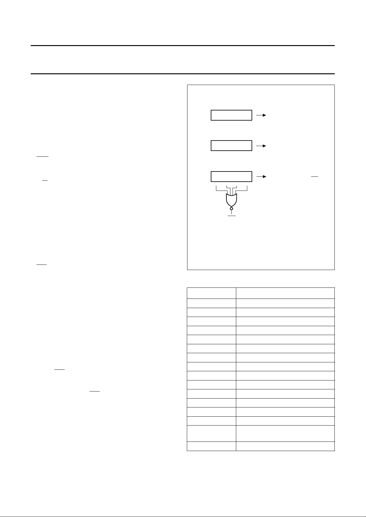
7.4 Microcontroller interface
The microcontroller interface provides a means of
communication between a system controller (for instance
“Philips 90CE201”
) in a digital TV receiver and the
descrambler internal registers and buffers. The physical
interface consists of:
• DAT7 to DAT0; an 8-bit wide bidirectional data bus.
Data and address information are multiplexed on this
bus.
• DCS; an active LOW chip select signal.
The descrambler only responds to microcontroller
communication if this signal is driven LOW.
W; an active HIGH read signal, indicating that the
• R/
microcontroller is attempting to read data from registers
or buffers inside the descrambler. If this signal is LOW,
data is being written to registers or buffers inside the
descrambler.
• A1 and A0; a 2-bit address bus. If the least significant
address bit (0) is logic 0, the most significant byte of a
16-bit register is addressed, otherwise the least
significant byte is selected. If the most significant
address bit (1) is logic 1 DAT7 to DAT0 carries the
address information, otherwise it will carry control data.
• IRQ; an active LOW (open-drain output) interrupt
request signal. An interrupt is set if one of the15 bits in
the descramblers internal interrupt register is set.
The interrupt mechanism consists of three 15-bit
registers and one 4-bit register, as illustrated in Fig.8.
The interrupt status register enables the microcontroller
to monitor the momentary status of the interrupts.
This is particularly useful during read operations in the
descramblers CA buffers, as the interrupt status bits in
question [‘flt0_stat’, ‘flt1_stat’, etc. (see Table 10,
addresses 0x0002 and 0x0004)] are reset when the
buffers have been emptied or released.
The interrupt mask register (see Table 10,
address 0x0001) prevents individual interrupts from
resetting IRQ (to logic 0). The interrupt status bits are
logically ANDed with the mask. If a rising edge occurs on
one of the resulting signals, it is latched into the interrupt
register, thus resetting IRQ.
handbook, halfpage
The interrupt register is reset when addressed.
0x0002/0x0004
(read only)
19-bit status
0x0001
(write only)
15-bit mask
0x0000
(read/write)
15-bit interrupt
IRQ
momentary status of the
individual interrupt bits
enables/disables
individual interrupts
latched interrupts, indicating
which interrupt(s) set IRQ
MGG320
Fig.8 Descrambler version 3, microcontroller
interrupt mechanism.
Table 6 Definition of interrupt mechanism; see Fig.8
BIT NUMBER MEANING OF INTERRUPT
0 filter 0 retrieved CA data
1 filter 1 retrieved CA data
2 filter 2 retrieved CA data
3 filter 3 retrieved CA data
4 filter 4 retrieved CA data
5 filter 5 retrieved CA data
6 filter 6 retrieved CA data
7 filter 7 retrieved CA data
8 filter 8 retrieved CA data
9 filter 9 retrieved CA data
10 filter 10 retrieved CA data
11 filter 11 retrieved CA data
12 filter 12 retrieved CA data
13 filter 13 retrieved CA data
14 filter 14, 15, 16 or 17 retrieved
CA data
15 empty
1996 Oct 09 15
Page 16
Philips Semiconductors Product specification
DVB compliant descrambler SAA7206H
The interrupt register itself is reset
(to 0000000000000000) as soon as it is addressed
(0x0000) by the microcontroller.
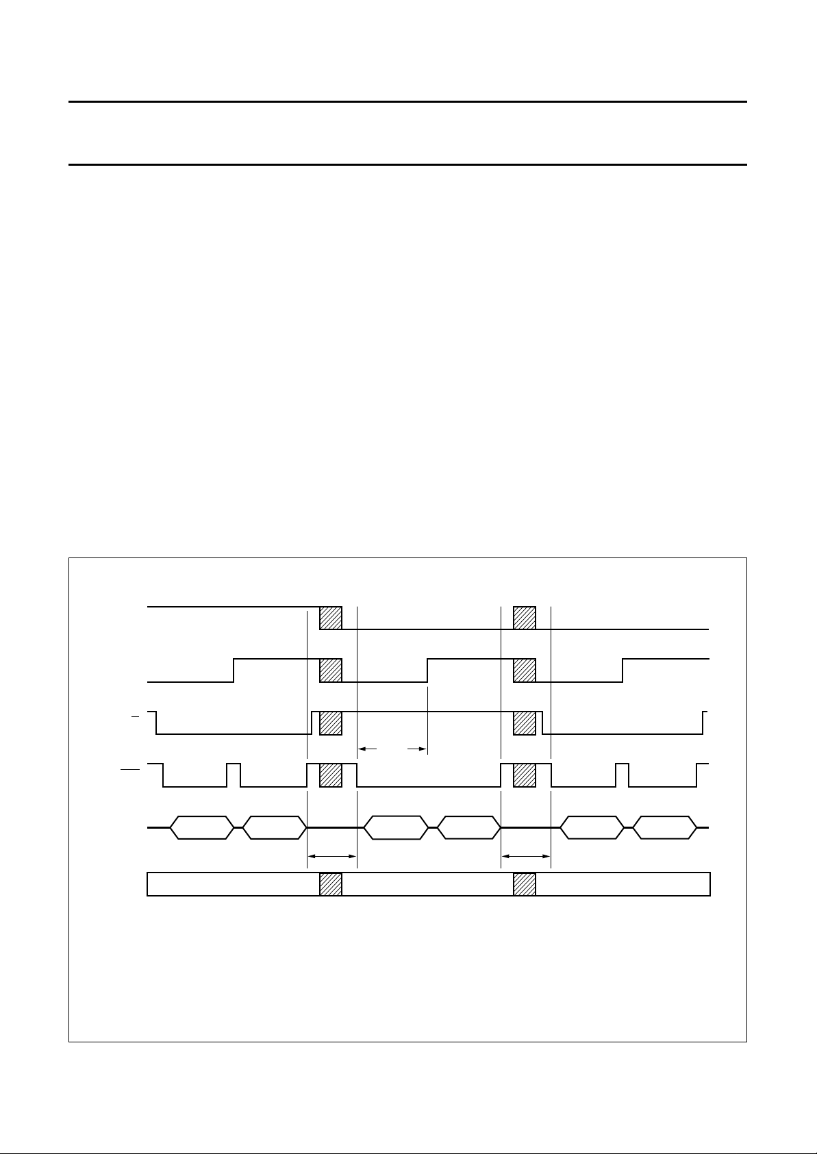
A typical example of communication between
microcontroller and descrambler is illustrated in Fig.9.
The descrambler contains an auto increment address
counter which can be loaded by performing a write
address operation. The present operation, whether read or
write, is now performed on the current address. The next
operation, whether read or write, is performed on the
current address plus 1.
Remark: Avoid resetting the auto increment address
counter to 0x0000, when not handling interrupts, as
addressing it causes the interrupt register to be reset.
Consequently, interrupt information might be lost.
The descrambler internal register and buffer addresses
are organized as illustrated in Fig.10. The first 4 address
bits (15 to 12) are used to select either the descrambler
registers (equals 0) or one of the descrambler buffers
(ranges 1 and 2).
In the buffer mode, the remaining address bits (11 to 0) are
part of the word address (range depending on the buffer,
see Table 10). In the register mode, bits 11 to 8 specify
the register unit number (see Fig.10). The remaining 8 bits
of the address (7 to 0) indicate specific register addresses
within a selected unit. The address range in a specific
register unit depends on the number of registers present
and is different for each unit. For details refer to Table 10.
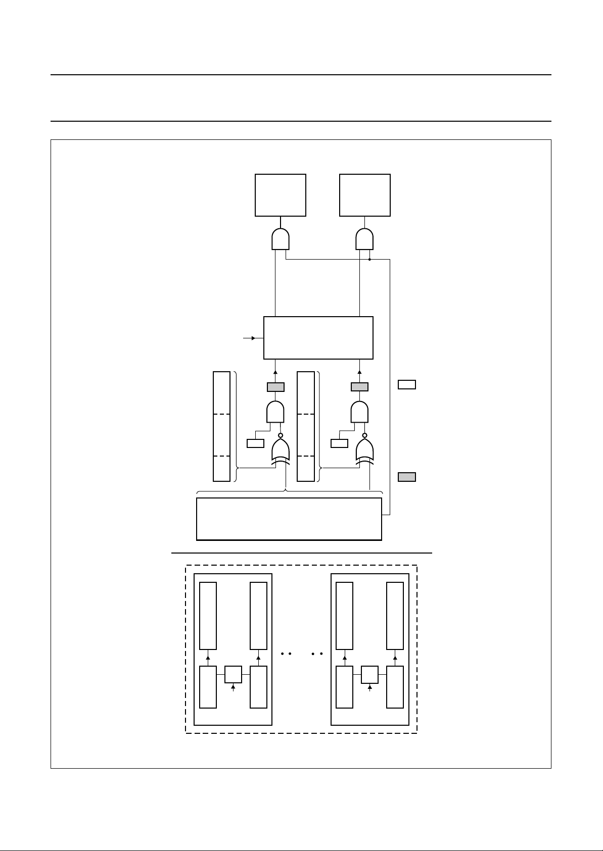
The CA filter module in the microcontroller interface unit is
capable of accessing general CA messages (ECM and
EMM, etc.) in the transport stream. The CA filter module
consists of 18 filters and 18 buffers of 256 bytes each,
thus each filter has its own data buffer. The 18 filters are
divided into two types of filters, which are specified in
Table 9. For each filter the ‘table_id’ of the section (the first
byte of the section see Fig.9), can be masked.
The architecture of the 9 CA filter pairs is shown in Fig.11.
handbook, full pagewidth
A1
A0
R/W
DCS
DAT7 to
DAT0
The descrambler internal register address is incremented automatically.
MSByte LSByte MSByte LSByte MSByte LSByte
>666 ns >666 ns
write address N read data @ N write data @ N+1
>24 ns
MGG321
Fig.9 Microcontroller descrambler communication (example).
1996 Oct 09 16
Page 17

Philips Semiconductors Product specification
DVB compliant descrambler SAA7206H
Table 7 Buffer contents
BUFFER NUMBER BUFFER CONTENTS
handbook, halfpage
(1)
(2)
if 0, registers are addressed,
if >0, buffers are addressed
register unit number, range 0 to 3
individual register addresses,
range depending on the unit
number
1 CW bank
2 CA data buffers for filters 0 to 15
3 CA data buffers for filters
16 and 17
Table 8 Unit contents
0 x H H H H
(1) See Table 7.
(2) See Table 8.
MGG322
REGISTER UNIT
NUMBER
0 interrupt request handling control
1 parser input control
UNIT CONTENTS
2 PID filter bank control
Fig.10 Descrambler, register organization
3 CA filtering control
(see Table 10).
Table 9 Specification of the number of CA_data_bytes which can be used for address filtering in the three types of
filters in the CA filter module (all bits in the filter can be masked individually)
FILTER NUMBER NUMBER OF FILTERS FILTER LENGTH (BYTES) PID MASKABLE
Filters 0 to 15 16 7 no
Filters 16 and 17
2 17 yes
(DVB compliant)
The filter consists of 18 section detectors. Each section
detector selects and retrieves section data for
CA_messages on the basis of:
• PID; which is maskable only for filters 16 and 17
• Table_id; which is maskable for all filters
• For filters 0 to 15; the first 7 bytes in the section payload,
which are maskable for all filters (see Fig.4)
• For filters 16 and 17; the first 17 bytes in the section
payload, which are maskable
• For all filters (see Fig.4).
The maximum section length of a conditional access
message is 256 bytes. If the section length of a message
is higher, data acquisition into the buffer is stopped after
256 bytes and an interrupt signal (plus filter fired signal) is
generated as normal. In this (erroneous) situation the
‘section_to_long’ bit of the filter is also set, which can be
read by the microcontroller (see Table 10).
The CA filters allow retrieval of multiple consecutive CA
messages, even if these messages have identical
selection criteria. For this purpose the 18 filters are
grouped in 9 filter pairs (0 and 1, 2 and 3 to 16 and 17).
Each of the CA filters in a pair can be programmed
The CA data detected by a certain filter is stored in the
256 byte buffer, only if its buffer is empty. As soon as an
entire section of CA data is stored, an interrupt is
generated (see Table 10, address 0x0000).
The 18 section detectors can be separately enabled, to
avoid unnecessary interrupts. The ‘filter fired’ registers
enable the microcontroller to track which filter caused a
buffer to be loaded (see Table 10, addresses 0x0300 and
0x0301).
equivalently. To prevent two filters from firing at the same
time the ‘equal conditions’ bits of the appropriate filter pair
can be programmed to logic 1. As a result, the filter with
the even (equals lowest) index number (for instance
filter_8 of filter pair 8 and 9) fires at the first occurrence of
a matching section. If, at the time of the second occurrence
of a matching section, the buffer of the filter with the even
index number is still occupied, the other filter (with odd
index number) of a filter pair fires, thus storing the section
data in its buffer.
1996 Oct 09 17
Page 18

Philips Semiconductors Product specification
DVB compliant descrambler SAA7206H
If the microcontroller decides to read data from one of the
CA buffers (see Table 10, address range filter_0:
0x2000 to 0x207F to filter_17: 0x2880 to 0x28FF) it can
determine when to stop reading in two ways. It can
periodically poll the ‘flt0_stat’ to ‘flt17_stat’ bits in the
interrupt status register (see Table 10, address 0x0002
and 0x0004). Each of these bits goes LOW as soon as the
last valid section data is read from the associated CA
buffer.
Another possibility is to read the ‘high_flt_address’ word
(‘haddr7 to 0’, Table 10, addresses 0x0302 to 0x0313).
The high address indicates the number of valid section
words (1 word = 2 bytes) that were written into the buffer.
This number equals the number of read cycles that has to
be performed to retrieve all valid data from the buffer.
If the buffer contents have to be removed without being
read, the microcontroller can write a logic 1 to the
‘rst_bf17-0’ bit (see Table 10, address 0x0314 and
0x0315) thus releasing the buffer. Another possibility is to
perform a write address operation with a value of
haddr7 to haddr0 plus buffer base address. The internal
auto increment address counter is thus set to the last word
in the buffer, causing the interrupt status bit to be reset and
the filters to be reactivated, after having been idle during
buffer emptying.
7.5 Output interfacing
The output data stream consists of a sequence of bytes.
A new byte is present at the data output pins
DATO7 to DATO0 at each rising edge of the descrambler
chip clock DCLK. The control signals SYNCO and DVO
are a delayed (9 MHz) version of the input interface signals
MSYNC and MDV respectively. By this form of delay
correction the relationship between the data and control
signals is maintained.
The
MB/MB and MBCLK signals are not output to the
demultiplexer. The descrambler converts the
signal to the transport_error_indicator bit in the TS
packets. At the descrambler output all information is
consequently contained in the stream. MBCLK is only
used to clock data into the descrambler, interfacing to the
demultiplexer is performed using the 9 MHz DCLK, which
is generated by the demultiplexer.
7.6 Boundary scan test
The DVB compliant descrambler is equipped with a 5-pins
test port interface for Boundary Scan Test (BST).
The implementation is in accordance with the BST
standard.
MB/MB
If, during the acquisition of a CA message, one of the TS
packets composing a message contains an error
(‘transport_error_indicator’ = ‘1’) the erroneous TS packet
is removed and CA message acquisition is restarted. Thus
the complete CA message is lost when at least one of the
TS packets which composes this message contains an
error. Duplicate TS packets containing CA messages are
also removed.
1996 Oct 09 18
Page 19
Philips Semiconductors Product specification
DVB compliant descrambler SAA7206H
handbook, full pagewidth
equal
conditions
CA filter pair architecture
PID r table_id y address c
CA
BUFFER
interrupt to
microcontroller
(256 bytes)
PID s table_id z address d
CA
BUFFER
(256 bytes)
interrupt to
microcontroller
MGG323
= filter fired indicator = filter enable
INPUT
STREAM
256B BUFFER_0
256B BUFFER_1
CA module structure
FILTER 0
equal
conditions
FILTER 1
1996 Oct 09 19
256B BUFFER_16
identical filter (pairs) 2 to15
FILTER 16
equal
conditions
Fig.11 CA two filter architecture.
256B BUFFER_17
FILTER 17
Page 20

Philips Semiconductors Product specification
DVB compliant descrambler SAA7206H
9 MHz_
interface
polarity
BITS
15/7 14/6 13/5 12/4 11/3 10/2 9/1 8/0
(HEX)
ADDRESS
flt7_irp flt6_irp flt5_irp flt4_irp flt3_irp flt2_irp flt1_irpt flt0_irpt
msk7 msk6 msk5 msk4 msk3 msk2 msk1 msk0
−−−−flt17_stat flt16_stat flt15_stat flt14_stat
−− −−−−−−
−− −−−−−−
−− −−−−bad_
−− −−−−−−
00 000011
flt7_stat flt6_stat flt5_stat flt4_stat flt3_stat flt2_stat flt1_stat flt0_stat
W −−−−−−−−
0x0003- R −−−−−−−−
0x0004- R −−−−−−−−
0x00FF
−− −−−−−−
pid4 pid3 pid2 pid1 pid0 cwpi2 cwpi1 cwpi0
pid4 pid3 pid2 pid1 pid0 cwpi2 cwpi1 cwpi0
pid4 pid3 pid2 pid1 pid0 cwpi2 cwpi1 cwpi0
pid4 pid3 pid2 pid1 pid0 cwpi2 cwpi1 cwpi0
pid4 pid3 pid2 pid1 pid0 cwpi2 cwpi1 cwpi0
W pid12 pid11 pid10 pid9 pid8 pid7 pid6 pid5
W pid12 pid11 pid10 pid9 pid8 pid7 pid6 pid5
W pid12 pid11 pid10 pid9 pid8 pid7 pid6 pid5
W pid12 pid11 pid10 pid9 pid8 pid7 pid6 pid5
W pid12 pid11 pid10 pid9 pid8 pid7 pid6 pid5
W pid12 pid11 pid10 pid9 pid8 pid7 pid6 pid5
0x01FF
pid4 pid3 pid2 pid1 pid0 cwpi2 cwpi1 cwpi0
REGISTER
FUNCTION
IRPT_ STATUS 0x0002- R − flt14-17_stat flt13_stat flt12_stat flt11_stat flt10_stat flt9_stat flt8_stat
CHIP_
IDENTIFICATION
IRPT_ STATUS_
FLT14-17
IRPT_ MASK 0x0001- R/W − msk14 msk13 msk12 msk11 msk10 msk9 msk8
7.7 Programming the descrambler
Table 10 Descrambler programming.
1996 Oct 09 20
IRPT 0x0000- R/W flt14-17_irp flt13_irp flt12_irp flt11_irp flt10_irp flt9_irp flt8_irp
EMPTY 0x0005 to
PRS_INP CTRL 0x0100-
EMPTY 0x0101 to
PID0, CWPI0 0x0200-
PID1, CWPI1 0x0201-
PID2, CWPI2 0x0202-
PID3, CWPI3 0x0203-
PID4, CWPI4 0x0204-
PID5, CWPI5 0x0205-
Page 21

Philips Semiconductors Product specification
DVB compliant descrambler SAA7206H
msk0
msk8
pid5_
ts_sc_
ts_sc_
is_pes
ts_sc_
is_pes
is_pes
pid4_0
pid4_1
pid5_0
pid5_1
DCW_valid
PID0_
PID1_
PID2_
ts_sc_
pid0_0
ts_sc_
pid0_1
ts_sc_
pid1_0
ts_sc_
pid1_1
pid4_0
pes_sc_
pid4_1
pes_sc_
pid5_0
pes_sc_
pid5_1
pid5_
pid0_0
pes_sc_
pid5_
pid0_1
pes_sc_
pid5_
pid1_0
pes_sc_
pid5_
pid1_1
pes_sc_
msk9
pid5_
pid5_
msk10
pid5_
msk11
msk1
msk2
msk3
BITS
15/7 14/6 13/5 12/4 11/3 10/2 9/1 8/0
(HEX)
ADDRESS
PID3_
is_pes
PID4_
is_pes
is_pes
−PID5_
ts_sc_
pid2_0
ts_sc_
pid2_1
ts_sc_
pid3_0
ts_sc_
pid3_1
pid2_0
pes_sc_
pid2_1
pes_sc_
pid3_0
pes_sc_
pid3_1
pes_sc_
W −−−pid5_
pid5_
msk12
pid5_
pid5_
pid5_
msk4
msk5
msk6
−− −−−−−−
−− −−−−−−
msk7
0x02FF
−− −−−−flt17_frd flt16_frd
0x0300- R −−−−−−−−
−−−−−−−
flt7_frd flt6_frd flt5_frd flt4_frd flt3_frd flt2_frd flt1_frd flt0_frd
0x0301- R flt15_frd flt14_frd flt13_frd flt12_frd flt11_frd flt10_frd flt9_frd flt8_frd
−−−−−−−
to_long
hadr0_7 hadr0_6 hadr0_5 hadr0_4 hadr0_3 hadr0_2 hadr0_1 hadr0_0
−−−−−−−
to_long
hadr1_7 hadr1_6 hadr1_5 hadr1_4 hadr1_3 hadr1_2 hadr1_1 hadr1_0
−−−−−−−
to_long
hadr2_7 hadr2_6 hadr2_5 hadr2_4 hadr2_3 hadr2_2 hadr2_1 hadr2_0
to_long
hadr3_7 hadr3_6 hadr3_5 hadr3_4 hadr3_3 hadr3_2 hadr3_1 hadr3_0
REGISTER
FUNCTION
DCW_ VALID 0x0206- W −−−−−−−−
1996 Oct 09 21
TS_SCR_ CTRL 0x0207- R −−−−ts_sc_
PES_SCR_CTRL 0x0208- R −−−−pes_sc_
PID5_MASK 0x0209-
EMPTY 0x0210 to
FLT17-16 FIRED
STATUS
FLT15-0 FIRED
STATUS
FLT0 STATUS 0x0302- R section
FLT1 STATUS 0x0303- R section
FLT2 STATUS 0x0304- R section
FLT3 STATUS 0x0305- R section
Page 22

Philips Semiconductors Product specification
DVB compliant descrambler SAA7206H
_0
hadr11
_1
hadr11
_2
hadr11
_3
hadr11
BITS
15/7 14/6 13/5 12/4 11/3 10/2 9/1 8/0
(HEX)
ADDRESS
_4
hadr11
_5
hadr11
−−−−−−−
−−−−−−−
to_long
to_long
hadr4_7 hadr4_6 hadr4_5 hadr4_4 hadr4_3 hadr4_2 hadr4_1 hadr4_0
−−−−−−−
to_long
hadr5_7 hadr5_6 hadr5_5 hadr5_4 hadr5_3 hadr5_2 hadr5_1 hadr5_0
−−−−−−−
hadr6_7 hadr6_6 hadr6_5 hadr6_4 hadr6_3 hadr6_2 hadr6_1 hadr6_0
−−−−−−−
to_long
hadr7_7 hadr7_6 hadr7_5 hadr7_4 hadr7_3 hadr7_2 hadr7_1 hadr7_0
−−−−−−−
to_long
hadr8_7 hadr8_6 hadr8_5 hadr8_4 hadr8_3 hadr8_2 hadr8_1 hadr8_0
−−−−−−−
to_long
hadr9_7 hadr9_6 hadr9_5 hadr9_4 hadr9_3 hadr9_2 hadr9_1 hadr9_0
−−−−−−−
to_long
to_long
hadr10_7 hadr10_6 hadr10_5 hadr10_4 hadr10_3 hadr10_2 hadr10_1 hadr10_0
−−−−−−−
_6
hadr11
_7
hadr11
−−−−−−−
to_long
to_long
hadr12_7 hadr12_6 hadr12_5 hadr12_4 hadr12_3 hadr12_2 hadr12_1 hadr12_0
hadr13_7 hadr13_6 hadr13_5 hadr13_4 hadr13_3 hadr13_2 hadr13_1 hadr13_0
REGISTER
FUNCTION
FLT4 STATUS 0x0306- R section
1996 Oct 09 22
FLT5 STATUS 0x0307- R section
FLT6 STATUS 0x0308- R section
FLT7 STATUS 0x0309- R section
FLT8 STATUS 0x030A- R section
FLT9 STATUS 0x030B- R section
FLT10 STATUS 0x030C- R section
FLT11 STATUS 0x030D- R section
FLT12 STATUS 0x030E- R section
FLT13 STATUS 0x030F- R section
Page 23

Philips Semiconductors Product specification
DVB compliant descrambler SAA7206H
BITS
15/7 14/6 13/5 12/4 11/3 10/2 9/1 8/0
(HEX)
ADDRESS
−−−−−−−
−−−−−−−
to_long
to_long
hadr14_7 hadr14_6 hadr14_5 hadr14_4 hadr14_3 hadr14_2 hadr14_1 hadr14_0
−−−−−−−
to_long
hadr15_7 hadr15_6 hadr15_5 hadr15_4 hadr15_3 hadr15_2 hadr15_1 hadr15_0
−−−−−−−
to_long
hadr16_7 hadr16_6 hadr16_5 hadr16_4 hadr16_3 hadr16_2 hadr16_1 hadr16_0
−− −−−−rst_bf17 rst_bf16
hadr17_7 hadr17_6 hadr17_5 hadr17_4 hadr17_3 hadr17_2 hadr17_1 hadr17_0
W −−−−−−−−
0x0314-
W rst_bf15 rst_bf14 rst_bf13 rst_bf12 rst_bf11 rst_bf10 rst_bf9 rst_bf8
0x0315-
rst_bf7 rst_bf6 rst_bf5 rst_bf4 rst_bf3 rst_bf2 rst_bf1 rst_bf0
W − equal_cond enable pid12 pid11 pid10 pid9 pid8
pid7 pid6 pid5 pid4 pid3 pid2 pid1 pid0
W msk7 msk6 msk5 msk4 msk3 msk2 msk1 msk0
tblid_7 tblid_6 tblid_5 tblid_4 tblid_3 tblid_2 tblid_1 tblid_0
W msk7 msk6 msk5 msk4 msk3 msk2 msk1 msk0
adr7 adr6 adr5 adr4 adr3 adr2 adr1 adr0
adr7 adr6 adr5 adr4 adr3 adr2 adr1 adr0
adr7 adr6 adr5 adr4 adr3 adr2 adr1 adr0
W msk7 msk6 msk5 msk4 msk3 msk2 msk1 msk0
adr7 adr6 adr5 adr4 adr3 adr2 adr1 adr0
adr7 adr6 adr5 adr4 adr3 adr2 adr1 adr0
W msk7 msk6 msk5 msk4 msk3 msk2 msk1 msk0
REGISTER
FUNCTION
FLT14 STATUS 0x0310- R section
1996 Oct 09 23
FLT15 STATUS 0x0311- R section
FLT16 STATUS 0x0312- R section
FLT17 STATUS 0x0313- R section
RESET BUFFER
RESET BUFFER
16 and 17
0to15
FLT0 CNTRL 0x0316-
FLT0 TBL_ID 0x0317-
FLT0 ADR BYTE0 0x0318-
FLT0 ADR BYTE1 0x0319- W msk7 msk6 msk5 msk4 msk3 msk2 msk1 msk0
FLT0 ADR BYTE2 0x031A- W msk7 msk6 msk5 msk4 msk3 msk2 msk1 msk0
FLT0 ADR BYTE3 0x031B-
FLT0 ADR BYTE4 0x031C-
Page 24

Philips Semiconductors Product specification
DVB compliant descrambler SAA7206H
BITS
15/7 14/6 13/5 12/4 11/3 10/2 9/1 8/0
(HEX)
ADDRESS
adr7 adr6 adr5 adr4 adr3 adr2 adr1 adr0
W msk7 msk6 msk5 msk4 msk3 msk2 msk1 msk0
adr7 adr6 adr5 adr4 adr3 adr2 adr1 adr0
W − equal_cond enable pid12 pid11 pid10 pid9 pid8
pid7 pid6 pid5 pid4 pid3 pid2 pid1 pid0
tblid_7 tblid_6 tblid_5 tblid_4 tblid_3 tblid_2 tblid_1 tblid_0
W msk7 msk6 msk5 msk4 msk3 msk2 msk1 msk0
adr7 adr6 adr5 adr4 adr3 adr2 adr1 adr0
W msk7 msk6 msk5 msk4 msk3 msk2 msk1 msk0
adr7 adr6 adr5 adr4 adr3 adr2 adr1 adr0
W msk7 msk6 msk5 msk4 msk3 msk2 msk1 msk0
W msk7 msk6 msk5 msk4 msk3 msk2 msk1 msk0
adr7 adr6 adr5 adr4 adr3 adr2 adr1 adr0
W msk7 msk6 msk5 msk4 msk3 msk2 msk1 msk0
adr7 adr6 adr5 adr4 adr3 adr2 adr1 adr0
adr7 adr6 adr5 adr4 adr3 adr2 adr1 adr0
W msk7 msk6 msk5 msk4 msk3 msk2 msk1 msk0
adr7 adr6 adr5 adr4 adr3 adr2 adr1 adr0
W msk7 msk6 msk5 msk4 msk3 msk2 msk1 msk0
adr7 adr6 adr5 adr4 adr3 adr2 adr1 adr0
W − equal_cond enable pid12 pid11 pid10 pid9 pid8
pid7 pid6 pid5 pid4 pid3 pid2 pid1 pid0
W msk7 msk6 msk5 msk4 msk3 msk2 msk1 msk0
tblid_7 tblid_6 tblid_5 tblid_4 tblid_3 tblid_2 tblid_1 tblid_0
W msk7 msk6 msk5 msk4 msk3 msk2 msk1 msk0
adr7 adr6 adr5 adr4 adr3 adr2 adr1 adr0
adr7 adr6 adr5 adr4 adr3 adr2 adr1 adr0
W msk7 msk6 msk5 msk4 msk3 msk2 msk1 msk0
REGISTER
FUNCTION
FLT1 ADR BYTE0 0x0321-
FLT1 ADR BYTE1 0x0322-
FLT0 ADR BYTE5 0x031D- W msk7 msk6 msk5 msk4 msk3 msk2 msk1 msk0
FLT0 ADR BYTE6 0x031E-
FLT1 CNTRL 0x031F-
1996 Oct 09 24
FLT1 TBL_ID 0x0320-
FLT1 ADR BYTE2 0x0323-
FLT1 ADR BYTE3 0x0324-
FLT1 ADR BYTE4 0x0325- W msk7 msk6 msk5 msk4 msk3 msk2 msk1 msk0
FLT1 ADR BYTE5 0x0326-
FLT1 ADR BYTE6 0x0327-
FLT2 CNTRL 0x0328-
FLT2 TBL_ID 0x0329-
FLT2 ADR BYTE0 0x032A-
FLT2 ADR BYTE1 0x032B-
Page 25

Philips Semiconductors Product specification
DVB compliant descrambler SAA7206H
BITS
15/7 14/6 13/5 12/4 11/3 10/2 9/1 8/0
(HEX)
ADDRESS
adr7 adr6 adr5 adr4 adr3 adr2 adr1 adr0
W msk7 msk6 msk5 msk4 msk3 msk2 msk1 msk0
adr7 adr6 adr5 adr4 adr3 adr2 adr1 adr0
W msk7 msk6 msk5 msk4 msk3 msk2 msk1 msk0
adr7 adr6 adr5 adr4 adr3 adr2 adr1 adr0
adr7 adr6 adr5 adr4 adr3 adr2 adr1 adr0
W msk7 msk6 msk5 msk4 msk3 msk2 msk1 msk0
adr7 adr6 adr5 adr4 adr3 adr2 adr1 adr0
W msk7 msk6 msk5 msk4 msk3 msk2 msk1 msk0
W − equal_cond enable pid12 pid11 pid10 pid9 pid8
pid7 pid6 pid5 pid4 pid3 pid2 pid1 pid0
W msk7 msk6 msk5 msk4 msk3 msk2 msk1 msk0
tblid_7 tblid_6 tblid_5 tblid_4 tblid_3 tblid_2 tblid_1 tblid_0
W msk7 msk6 msk5 msk4 msk3 msk2 msk1 msk0
adr7 adr6 adr5 adr4 adr3 adr2 adr1 adr0
adr7 adr6 adr5 adr4 adr3 adr2 adr1 adr0
W msk7 msk6 msk5 msk4 msk3 msk2 msk1 msk0
adr7 adr6 adr5 adr4 adr3 adr2 adr1 adr0
W msk7 msk6 msk5 msk4 msk3 msk2 msk1 msk0
adr7 adr6 adr5 adr4 adr3 adr2 adr1 adr0
W msk7 msk6 msk5 msk4 msk3 msk2 msk1 msk0
adr7 adr6 adr5 adr4 adr3 adr2 adr1 adr0
W msk7 msk6 msk5 msk4 msk3 msk2 msk1 msk0
adr7 adr6 adr5 adr4 adr3 adr2 adr1 adr0
W msk7 msk6 msk5 msk4 msk3 msk2 msk1 msk0
adr7 adr6 adr5 adr4 adr3 adr2 adr1 adr0
pid7 pid6 pid5 pid4 pid3 pid2 pid1 pid0
W − equal_cond enable pid12 pid11 pid10 pid9 pid8
REGISTER
FUNCTION
FLT3 CNTRL 0x0331-
FLT2 ADR BYTE2 0x032C- W msk7 msk6 msk5 msk4 msk3 msk2 msk1 msk0
FLT2 ADR BYTE3 0x032D-
FLT2 ADR BYTE4 0x032E-
1996 Oct 09 25
FLT2 ADR BYTE5 0x032F-
FLT2 ADR BYTE6 0x0330-
FLT3 TBL_ID 0x0332-
FLT3 ADR BYTE0 0x0333-
FLT3 ADR BYTE1 0x0334- W msk7 msk6 msk5 msk4 msk3 msk2 msk1 msk0
FLT3 ADR BYTE2 0x0335-
FLT3 ADR BYTE3 0x0336-
FLT3 ADR BYTE4 0x0337-
FLT3 ADR BYTE5 0x0338-
FLT3 DR BYTE6 0x0339-
FLT4 CNTRL 0x033A-
Page 26

Philips Semiconductors Product specification
DVB compliant descrambler SAA7206H
BITS
15/7 14/6 13/5 12/4 11/3 10/2 9/1 8/0
(HEX)
ADDRESS
tblid_7 tblid_6 tblid_5 tblid_4 tblid_3 tblid_2 tblid_1 tblid_0
W msk7 msk6 msk5 msk4 msk3 msk2 msk1 msk0
adr7 adr6 adr5 adr4 adr3 adr2 adr1 adr0
W msk7 msk6 msk5 msk4 msk3 msk2 msk1 msk0
adr7 adr6 adr5 adr4 adr3 adr2 adr1 adr0
adr7 adr6 adr5 adr4 adr3 adr2 adr1 adr0
W msk7 msk6 msk5 msk4 msk3 msk2 msk1 msk0
adr7 adr6 adr5 adr4 adr3 adr2 adr1 adr0
W msk7 msk6 msk5 msk4 msk3 msk2 msk1 msk0
adr7 adr6 adr5 adr4 adr3 adr2 adr1 adr0
W msk7 msk6 msk5 msk4 msk3 msk2 msk1 msk0
W msk7 msk6 msk5 msk4 msk3 msk2 msk1 msk0
adr7 adr6 adr5 adr4 adr3 adr2 adr1 adr0
W msk7 msk6 msk5 msk4 msk3 msk2 msk1 msk0
adr7 adr6 adr5 adr4 adr3 adr2 adr1 adr0
pid7 pid6 pid5 pid4 pid3 pid2 pid1 pid0
W msk7 msk6 msk5 msk4 msk3 msk2 msk1 msk0
tblid_7 tblid_6 tblid_5 tblid_4 tblid_3 tblid_2 tblid_1 tblid_0
W msk7 msk6 msk5 msk4 msk3 msk2 msk1 msk0
adr7 adr6 adr5 adr4 adr3 adr2 adr1 adr0
W msk7 msk6 msk5 msk4 msk3 msk2 msk1 msk0
adr7 adr6 adr5 adr4 adr3 adr2 adr1 adr0
adr7 adr6 adr5 adr4 adr3 adr2 adr1 adr0
W msk7 msk6 msk5 msk4 msk3 msk2 msk1 msk0
adr7 adr6 adr5 adr4 adr3 adr2 adr1 adr0
adr7 adr6 adr5 adr4 adr3 adr2 adr1 adr0
W msk7 msk6 msk5 msk4 msk3 msk2 msk1 msk0
REGISTER
FUNCTION
FLT4 ADR BYTE0 0x033C-
FLT4 TBL_ID 0x033B- W msk7 msk6 msk5 msk4 msk3 msk2 msk1 msk0
1996 Oct 09 26
FLT4 ADR BYTE1 0x033D-
FLT4 ADR BYTE2 0x033E-
FLT4 ADR BYTE3 0x033F-
FLT4 ADR BYTE4 0x0340-
FLT4 ADR BYTE5 0x0341-
FLT4 ADR BYTE6 0x0342-
FLT5 CNTRL 0x0343- W − equal_cond enable pid12 pid11 pid10 pid9 pid8
FLT5 TBL_ID 0x0344-
FLT5 ADR BYTE0 0x0345-
FLT5 ADR BYTE1 0x0346-
FLT5 ADR BYTE2 0x0347- W msk7 msk6 msk5 msk4 msk3 msk2 msk1 msk0
FLT5 ADR BYTE3 0x0348-
FLT5 ADR BYTE4 0x0349-
Page 27

Philips Semiconductors Product specification
DVB compliant descrambler SAA7206H
BITS
15/7 14/6 13/5 12/4 11/3 10/2 9/1 8/0
(HEX)
ADDRESS
adr7 adr6 adr5 adr4 adr3 adr2 adr1 adr0
W msk7 msk6 msk5 msk4 msk3 msk2 msk1 msk0
adr7 adr6 adr5 adr4 adr3 adr2 adr1 adr0
W − equal_cond enable pid12 pid11 pid10 pid9 pid8
pid7 pid6 pid5 pid4 pid3 pid2 pid1 pid0
tblid_7 tblid_6 tblid_5 tblid_4 tblid_3 tblid_2 tblid_1 tblid_0
W msk7 msk6 msk5 msk4 msk3 msk2 msk1 msk0
adr7 adr6 adr5 adr4 adr3 adr2 adr1 adr0
W msk7 msk6 msk5 msk4 msk3 msk2 msk1 msk0
adr7 adr6 adr5 adr4 adr3 adr2 adr1 adr0
W msk7 msk6 msk5 msk4 msk3 msk2 msk1 msk0
W msk7 msk6 msk5 msk4 msk3 msk2 msk1 msk0
adr7 adr6 adr5 adr4 adr3 adr2 adr1 adr0
W msk7 msk6 msk5 msk4 msk3 msk2 msk1 msk0
adr7 adr6 adr5 adr4 adr3 adr2 adr1 adr0
adr7 adr6 adr5 adr4 adr3 adr2 adr1 adr0
W msk7 msk6 msk5 msk4 msk3 msk2 msk1 msk0
adr7 adr6 adr5 adr4 adr3 adr2 adr1 adr0
W msk7 msk6 msk5 msk4 msk3 msk2 msk1 msk0
adr7 adr6 adr5 adr4 adr3 adr2 adr1 adr0
W − equal_cond enable pid12 pid11 pid10 pid9 pid8
pid7 pid6 pid5 pid4 pid3 pid2 pid1 pid0
W msk7 msk6 msk5 msk4 msk3 msk2 msk1 msk0
tblid_7 tblid_6 tblid_5 tblid_4 tblid_3 tblid_2 tblid_1 tblid_0
W msk7 msk6 msk5 msk4 msk3 msk2 msk1 msk0
adr7 adr6 adr5 adr4 adr3 adr2 adr1 adr0
adr7 adr6 adr5 adr4 adr3 adr2 adr1 adr0
W msk7 msk6 msk5 msk4 msk3 msk2 msk1 msk0
REGISTER
FUNCTION
FLT5 ADR BYTE5 0x034A- W msk7 msk6 msk5 msk4 msk3 msk2 msk1 msk0
FLT5 ADR BYTE6 0x034B-
FLT6 CNTRL 0x034C-
1996 Oct 09 27
FLT6 TBL_ID 0x034D-
FLT6 ADR BYTE0 0x034E-
FLT6 ADR BYTE1 0x034F-
FLT6 ADR BYTE2 0x0350-
FLT6 ADR BYTE3 0x0351-
FLT6 ADR BYTE4 0x0352- W msk7 msk6 msk5 msk4 msk3 msk2 msk1 msk0
FLT6 ADR BYTE5 0x0353-
FLT6 ADR BYTE6 0x0354-
FLT7 CNTRL 0x0355-
FLT7 TBL_ID 0x0356-
FLT7 ADR BYTE0 0x0357-
FLT7 ADR BYTE1 0x0358-
Page 28

Philips Semiconductors Product specification
DVB compliant descrambler SAA7206H
BITS
15/7 14/6 13/5 12/4 11/3 10/2 9/1 8/0
(HEX)
ADDRESS
adr7 adr6 adr5 adr4 adr3 adr2 adr1 adr0
W msk7 msk6 msk5 msk4 msk3 msk2 msk1 msk0
adr7 adr6 adr5 adr4 adr3 adr2 adr1 adr0
W msk7 msk6 msk5 msk4 msk3 msk2 msk1 msk0
adr7 adr6 adr5 adr4 adr3 adr2 adr1 adr0
adr7 adr6 adr5 adr4 adr3 adr2 adr1 adr0
W msk7 msk6 msk5 msk4 msk3 msk2 msk1 msk0
adr7 adr6 adr5 adr4 adr3 adr2 adr1 adr0
W msk7 msk6 msk5 msk4 msk3 msk2 msk1 msk0
W − equal_cond enable pid12 pid11 pid10 pid9 pid8
pid7 pid6 pid5 pid4 pid3 pid2 pid1 pid0
W msk7 msk6 msk5 msk4 msk3 msk2 msk1 msk0
tblid_7 tblid_6 tblid_5 tblid_4 tblid_3 tblid_2 tblid_1 tblid_0
W msk7 msk6 msk5 msk4 msk3 msk2 msk1 msk0
adr7 adr6 adr5 adr4 adr3 adr2 adr1 adr0
adr7 adr6 adr5 adr4 adr3 adr2 adr1 adr0
W msk7 msk6 msk5 msk4 msk3 msk2 msk1 msk0
adr7 adr6 adr5 adr4 adr3 adr2 adr1 adr0
W msk7 msk6 msk5 msk4 msk3 msk2 msk1 msk0
adr7 adr6 adr5 adr4 adr3 adr2 adr1 adr0
W msk7 msk6 msk5 msk4 msk3 msk2 msk1 msk0
adr7 adr6 adr5 adr4 adr3 adr2 adr1 adr0
W msk7 msk6 msk5 msk4 msk3 msk2 msk1 msk0
adr7 adr6 adr5 adr4 adr3 adr2 adr1 adr0
W msk7 msk6 msk5 msk4 msk3 msk2 msk1 msk0
adr7 adr6 adr5 adr4 adr3 adr2 adr1 adr0
pid7 pid6 pid5 pid4 pid3 pid2 pid1 pid0
W − equal_cond enable pid12 pid11 pid10 pid9 pid8
REGISTER
FUNCTION
FLT7 ADR BYTE3 0x035A-
FLT7 ADR BYTE2 0x0359- W msk7 msk6 msk5 msk4 msk3 msk2 msk1 msk0
1996 Oct 09 28
FLT7 ADR BYTE4 0x035B-
FLT7 ADR BYTE5 0x035C-
FLT7 ADR BYTE6 0x035D-
FLT8 CNTRL 0x035E-
FLT8 TBL_ID 0x031F-
FLT8 ADR BYTE0 0x0360-
FLT8 ADR BYTE1 0x0361- W msk7 msk6 msk5 msk4 msk3 msk2 msk1 msk0
FLT8 ADR BYTE2 0x0362-
FLT8 ADR BYTE3 0x0363-
FLT8 ADR BYTE4 0x0364-
FLT8 ADR BYTE5 0x0365-
FLT8 ADR BYTE6 0x0366-
FLT9 CNTRL 0x0367-
Page 29

Philips Semiconductors Product specification
DVB compliant descrambler SAA7206H
BITS
15/7 14/6 13/5 12/4 11/3 10/2 9/1 8/0
(HEX)
ADDRESS
tblid_7 tblid_6 tblid_5 tblid_4 tblid_3 tblid_2 tblid_1 tblid_0
W msk7 msk6 msk5 msk4 msk3 msk2 msk1 msk0
adr7 adr6 adr5 adr4 adr3 adr2 adr1 adr0
W msk7 msk6 msk5 msk4 msk3 msk2 msk1 msk0
adr7 adr6 adr5 adr4 adr3 adr2 adr1 adr0
adr7 adr6 adr5 adr4 adr3 adr2 adr1 adr0
W msk7 msk6 msk5 msk4 msk3 msk2 msk1 msk0
adr7 adr6 adr5 adr4 adr3 adr2 adr1 adr0
W msk7 msk6 msk5 msk4 msk3 msk2 msk1 msk0
adr7 adr6 adr5 adr4 adr3 adr2 adr1 adr0
W msk7 msk6 msk5 msk4 msk3 msk2 msk1 msk0
W msk7 msk6 msk5 msk4 msk3 msk2 msk1 msk0
adr7 adr6 adr5 adr4 adr3 adr2 adr1 adr0
W msk7 msk6 msk5 msk4 msk3 msk2 msk1 msk0
adr7 adr6 adr5 adr4 adr3 adr2 adr1 adr0
pid7 pid6 pid5 pid4 pid3 pid2 pid1 pid0
W msk7 msk6 msk5 msk4 msk3 msk2 msk1 msk0
tblid_7 tblid_6 tblid_5 tblid_4 tblid_3 tblid_2 tblid_1 tblid_0
W msk7 msk6 msk5 msk4 msk3 msk2 msk1 msk0
0x0372-
adr7 adr6 adr5 adr4 adr3 adr2 adr1 adr0
adr7 adr6 adr5 adr4 adr3 adr2 adr1 adr0
W msk7 msk6 msk5 msk4 msk3 msk2 msk1 msk0
0x0373-
adr7 adr6 adr5 adr4 adr3 adr2 adr1 adr0
W msk7 msk6 msk5 msk4 msk3 msk2 msk1 msk0
0x0374-
adr7 adr6 adr5 adr4 adr3 adr2 adr1 adr0
W msk7 msk6 msk5 msk4 msk3 msk2 msk1 msk0
0x0375-
adr7 adr6 adr5 adr4 adr3 adr2 adr1 adr0
W msk7 msk6 msk5 msk4 msk3 msk2 msk1 msk0
0x0376-
REGISTER
FUNCTION
FLT9 ADR BYTE0 0x0369-
FLT9 TBL_ID 0x0368- W msk7 msk6 msk5 msk4 msk3 msk2 msk1 msk0
1996 Oct 09 29
FLT9 ADR BYTE1 0x036A-
FLT9 ADR BYTE2 0x036B-
FLT9 ADR BYTE3 0x036C-
FLT9 ADR BYTE4 0x036D-
FLT9 ADR BYTE5 0x036E-
FLT10 CNTRL 0x0370- W − equal_cond enable pid12 pid11 pid10 pid9 pid8
FLT9 ADR BYTE6 0x0363F-
FLT10 TBL_ID 0x0371-
FLT10 ADR
BYTE0
FLT10 ADR
BYTE1
FLT10 ADR
BYTE2
FLT10 ADR
BYTE3
FLT10 ADR
BYTE4
Page 30

Philips Semiconductors Product specification
DVB compliant descrambler SAA7206H
BITS
15/7 14/6 13/5 12/4 11/3 10/2 9/1 8/0
(HEX)
ADDRESS
0x0377- W msk7 msk6 msk5 msk4 msk3 msk2 msk1 msk0
adr7 adr6 adr5 adr4 adr3 adr2 adr1 adr0
adr7 adr6 adr5 adr4 adr3 adr2 adr1 adr0
W msk7 msk6 msk5 msk4 msk3 msk2 msk1 msk0
0x0378-
W − equal_cond enable pid12 pid11 pid10 pid9 pid8
pid7 pid6 pid5 pid4 pid3 pid2 pid1 pid0
tblid_7 tblid_6 tblid_5 tblid_4 tblid_3 tblid_2 tblid_1 tblid_0
W msk7 msk6 msk5 msk4 msk3 msk2 msk1 msk0
adr7 adr6 adr5 adr4 adr3 adr2 adr1 adr0
W msk7 msk6 msk5 msk4 msk3 msk2 msk1 msk0
0x037B-
adr7 adr6 adr5 adr4 adr3 adr2 adr1 adr0
W msk7 msk6 msk5 msk4 msk3 msk2 msk1 msk0
0x037C-
adr7 adr6 adr5 adr4 adr3 adr2 adr1 adr0
W msk7 msk6 msk5 msk4 msk3 msk2 msk1 msk0
0x037D-
adr7 adr6 adr5 adr4 adr3 adr2 adr1 adr0
W msk7 msk6 msk5 msk4 msk3 msk2 msk1 msk0
0x037E-
0x037F- W msk7 msk6 msk5 msk4 msk3 msk2 msk1 msk0
adr7 adr6 adr5 adr4 adr3 adr2 adr1 adr0
adr7 adr6 adr5 adr4 adr3 adr2 adr1 adr0
W msk7 msk6 msk5 msk4 msk3 msk2 msk1 msk0
0x0380-
adr7 adr6 adr5 adr4 adr3 adr2 adr1 adr0
W msk7 msk6 msk5 msk4 msk3 msk2 msk1 msk0
0x0381-
W − equal_cond enable pid12 pid11 pid10 pid9 pid8
pid7 pid6 pid5 pid4 pid3 pid2 pid1 pid0
tblid_7 tblid_6 tblid_5 tblid_4 tblid_3 tblid_2 tblid_1 tblid_0
W msk7 msk6 msk5 msk4 msk3 msk2 msk1 msk0
0x0384-
adr7 adr6 adr5 adr4 adr3 adr2 adr1 adr0
adr7 adr6 adr5 adr4 adr3 adr2 adr1 adr0
W msk7 msk6 msk5 msk4 msk3 msk2 msk1 msk0
0x0385-
REGISTER
FUNCTION
FLT11 ADR
FLT10 ADR
BYTE6
FLT10 ADR
BYTE5
1996 Oct 09 30
FLT11 CNTRL 0x0379-
FLT11 TBL_ID 0x037A-
BYTE0
FLT11 ADR
FLT11 ADR
BYTE1
BYTE2
FLT11 ADR
BYTE3
FLT11 ADR
BYTE4
FLT11 ADR
BYTE5
FLT11 ADR
BYTE6
FLT12 CNTRL 0x0382-
FLT12 TBL_ID 0x0383- W msk7 msk6 msk5 msk4 msk3 msk2 msk1 msk0
FLT12 ADR
BYTE0
FLT12 ADR
BYTE1
Page 31

Philips Semiconductors Product specification
DVB compliant descrambler SAA7206H
BITS
15/7 14/6 13/5 12/4 11/3 10/2 9/1 8/0
(HEX)
ADDRESS
0x0386- W msk7 msk6 msk5 msk4 msk3 msk2 msk1 msk0
adr7 adr6 adr5 adr4 adr3 adr2 adr1 adr0
adr7 adr6 adr5 adr4 adr3 adr2 adr1 adr0
W msk7 msk6 msk5 msk4 msk3 msk2 msk1 msk0
0x0387-
adr7 adr6 adr5 adr4 adr3 adr2 adr1 adr0
W msk7 msk6 msk5 msk4 msk3 msk2 msk1 msk0
0x0388-
adr7 adr6 adr5 adr4 adr3 adr2 adr1 adr0
W msk7 msk6 msk5 msk4 msk3 msk2 msk1 msk0
0x0389-
adr7 adr6 adr5 adr4 adr3 adr2 adr1 adr0
W msk7 msk6 msk5 msk4 msk3 msk2 msk1 msk0
0x038A-
W − equal_cond enable pid12 pid11 pid10 pid9 pid8
pid7 pid6 pid5 pid4 pid3 pid2 pid1 pid0
W msk7 msk6 msk5 msk4 msk3 msk2 msk1 msk0
tblid_7 tblid_6 tblid_5 tblid_4 tblid_3 tblid_2 tblid_1 tblid_0
W msk7 msk6 msk5 msk4 msk3 msk2 msk1 msk0
0x038D-
adr7 adr6 adr5 adr4 adr3 adr2 adr1 adr0
0x038E- W msk7 msk6 msk5 msk4 msk3 msk2 msk1 msk0
adr7 adr6 adr5 adr4 adr3 adr2 adr1 adr0
adr7 adr6 adr5 adr4 adr3 adr2 adr1 adr0
W msk7 msk6 msk5 msk4 msk3 msk2 msk1 msk0
0x038F-
adr7 adr6 adr5 adr4 adr3 adr2 adr1 adr0
W msk7 msk6 msk5 msk4 msk3 msk2 msk1 msk0
0x0390-
adr7 adr6 adr5 adr4 adr3 adr2 adr1 adr0
W msk7 msk6 msk5 msk4 msk3 msk2 msk1 msk0
0x0391-
adr7 adr6 adr5 adr4 adr3 adr2 adr1 adr0
W msk7 msk6 msk5 msk4 msk3 msk2 msk1 msk0
0x0392-
adr7 adr6 adr5 adr4 adr3 adr2 adr1 adr0
W msk7 msk6 msk5 msk4 msk3 msk2 msk1 msk0
0x0393-
pid7 pid6 pid5 pid4 pid3 pid2 pid1 pid0
W − equal_cond enable pid12 pid11 pid10 pid9 pid8
REGISTER
FUNCTION
FLT12 ADR
BYTE3
FLT12 ADR
BYTE4
FLT12 ADR
BYTE5
FLT12 ADR
FLT12 ADR
BYTE2
1996 Oct 09 31
BYTE6
FLT13 CNTRL 0x038B-
FLT13 TBL_ID 0x038C-
FLT13 ADR
BYTE0
FLT13 ADR
BYTE1
FLT13 ADR
FLT13 ADR
BYTE2
FLT13 ADR
BYTE3
BYTE4
FLT13 ADR
BYTE5
FLT13 ADR
BYTE6
FLT14 CNTRL 0x0394-
Page 32

Philips Semiconductors Product specification
DVB compliant descrambler SAA7206H
BITS
15/7 14/6 13/5 12/4 11/3 10/2 9/1 8/0
(HEX)
ADDRESS
tblid_7 tblid_6 tblid_5 tblid_4 tblid_3 tblid_2 tblid_1 tblid_0
W msk7 msk6 msk5 msk4 msk3 msk2 msk1 msk0
0x0396-
adr7 adr6 adr5 adr4 adr3 adr2 adr1 adr0
adr7 adr6 adr5 adr4 adr3 adr2 adr1 adr0
W msk7 msk6 msk5 msk4 msk3 msk2 msk1 msk0
0x0397-
adr7 adr6 adr5 adr4 adr3 adr2 adr1 adr0
W msk7 msk6 msk5 msk4 msk3 msk2 msk1 msk0
0x0398-
adr7 adr6 adr5 adr4 adr3 adr2 adr1 adr0
W msk7 msk6 msk5 msk4 msk3 msk2 msk1 msk0
0x0399-
adr7 adr6 adr5 adr4 adr3 adr2 adr1 adr0
W msk7 msk6 msk5 msk4 msk3 msk2 msk1 msk0
0x039A-
adr7 adr6 adr5 adr4 adr3 adr2 adr1 adr0
W msk7 msk6 msk5 msk4 msk3 msk2 msk1 msk0
0x039B-
adr7 adr6 adr5 adr4 adr3 adr2 adr1 adr0
W msk7 msk6 msk5 msk4 msk3 msk2 msk1 msk0
0x039C-
pid7 pid6 pid5 pid4 pid3 pid2 pid1 pid0
W msk7 msk6 msk5 msk4 msk3 msk2 msk1 msk0
tblid_7 tblid_6 tblid_5 tblid_4 tblid_3 tblid_2 tblid_1 tblid_0
W msk7 msk6 msk5 msk4 msk3 msk2 msk1 msk0
0x039F-
adr7 adr6 adr5 adr4 adr3 adr2 adr1 adr0
W msk7 msk6 msk5 msk4 msk3 msk2 msk1 msk0
0x03A0-
adr7 adr6 adr5 adr4 adr3 adr2 adr1 adr0
adr7 adr6 adr5 adr4 adr3 adr2 adr1 adr0
W msk7 msk6 msk5 msk4 msk3 msk2 msk1 msk0
0x03A1-
adr7 adr6 adr5 adr4 adr3 adr2 adr1 adr0
W msk7 msk6 msk5 msk4 msk3 msk2 msk1 msk0
0x03A2-
adr7 adr6 adr5 adr4 adr3 adr2 adr1 adr0
W msk7 msk6 msk5 msk4 msk3 msk2 msk1 msk0
0x03A3-
REGISTER
FUNCTION
FLT14 ADR
BYTE0
FLT14 ADR
BYTE1
FLT14 ADR
BYTE2
FLT14 ADR
BYTE3
FLT14 ADR
FLT14 TBL_ID 0x0395- W msk7 msk6 msk5 msk4 msk3 msk2 msk1 msk0
1996 Oct 09 32
BYTE4
FLT14 ADR
BYTE5
FLT15 CNTRL 0x039D- W − equal_cond enable pid12 pid11 pid10 pid9 pid8
FLT14 ADR
BYTE6
FLT15 TBL_ID 0x039E-
FLT15 ADR
BYTE0
FLT15 ADR
BYTE1
FLT15 ADR
BYTE2
FLT15 ADR
BYTE3
FLT15 ADR
BYTE4
Page 33

Philips Semiconductors Product specification
DVB compliant descrambler SAA7206H
BITS
15/7 14/6 13/5 12/4 11/3 10/2 9/1 8/0
(HEX)
ADDRESS
0x03A4- W msk7 msk6 msk5 msk4 msk3 msk2 msk1 msk0
adr7 adr6 adr5 adr4 adr3 adr2 adr1 adr0
adr7 adr6 adr5 adr4 adr3 adr2 adr1 adr0
W msk7 msk6 msk5 msk4 msk3 msk2 msk1 msk0
0x03A5-
W −−−msk12 msk11 msk10 msk9 msk8
msk7 msk6 msk5 msk4 msk3 msk2 msk1 msk0
W − equal_cond enable pid12 pid11 pid10 pid9 pid8
pid7 pid6 pid5 pid4 pid3 pid2 pid1 pid0
tblid_7 tblid_6 tblid_5 tblid_4 tblid_3 tblid_2 tblid_1 tblid_0
W msk7 msk6 msk5 msk4 msk3 msk2 msk1 msk0
adr7 adr6 adr5 adr4 adr3 adr2 adr1 adr0
W msk7 msk6 msk5 msk4 msk3 msk2 msk1 msk0
0x03A9-
adr7 adr6 adr5 adr4 adr3 adr2 adr1 adr0
W msk7 msk6 msk5 msk4 msk3 msk2 msk1 msk0
0x03AA-
adr7 adr6 adr5 adr4 adr3 adr2 adr1 adr0
W msk7 msk6 msk5 msk4 msk3 msk2 msk1 msk0
0x03AB-
0x03AC- W msk7 msk6 msk5 msk4 msk3 msk2 msk1 msk0
adr7 adr6 adr5 adr4 adr3 adr2 adr1 adr0
W msk7 msk6 msk5 msk4 msk3 msk2 msk1 msk0
0x03AD-
adr7 adr6 adr5 adr4 adr3 adr2 adr1 adr0
adr7 adr6 adr5 adr4 adr3 adr2 adr1 adr0
W msk7 msk6 msk5 msk4 msk3 msk2 msk1 msk0
0x03AE-
adr7 adr6 adr5 adr4 adr3 adr2 adr1 adr0
W msk7 msk6 msk5 msk4 msk3 msk2 msk1 msk0
0x03AF-
adr7 adr6 adr5 adr4 adr3 adr2 adr1 adr0
W msk7 msk6 msk5 msk4 msk3 msk2 msk1 msk0
0x03B0-
adr7 adr6 adr5 adr4 adr3 adr2 adr1 adr0
W msk7 msk6 msk5 msk4 msk3 msk2 msk1 msk0
0x03B1-
adr7 adr6 adr5 adr4 adr3 adr2 adr1 adr0
W msk7 msk6 msk5 msk4 msk3 msk2 msk1 msk0
0x03B2-
REGISTER
FUNCTION
FLT16 CNTRL 0x03A7-
FLT16 TBL_ID 0x03A8-
FLT16 ADR
FLT15 ADR
BYTE5
FLT15 ADR
BYTE6
FLT16 PID MASK 0x03A6-
1996 Oct 09 33
BYTE0
FLT16 ADR
BYTE1
FLT16 ADR
BYTE2
FLT16 ADR
FLT16 ADR
BYTE3
BYTE4
FLT16 ADR
BYTE5
FLT16 ADR
FLT16 ADR
BYTE6
BYTE7
FLT16 ADR
BYTE8
FLT16 ADR
BYTE9
Page 34

Philips Semiconductors Product specification
DVB compliant descrambler SAA7206H
BITS
15/7 14/6 13/5 12/4 11/3 10/2 9/1 8/0
(HEX)
ADDRESS
0x03B3- W msk7 msk6 msk5 msk4 msk3 msk2 msk1 msk0
adr7 adr6 adr5 adr4 adr3 adr2 adr1 adr0
adr7 adr6 adr5 adr4 adr3 adr2 adr1 adr0
W msk7 msk6 msk5 msk4 msk3 msk2 msk1 msk0
0x03B4-
adr7 adr6 adr5 adr4 adr3 adr2 adr1 adr0
W msk7 msk6 msk5 msk4 msk3 msk2 msk1 msk0
0x03B5-
adr7 adr6 adr5 adr4 adr3 adr2 adr1 adr0
W msk7 msk6 msk5 msk4 msk3 msk2 msk1 msk0
0x03B6-
adr7 adr6 adr5 adr4 adr3 adr2 adr1 adr0
W msk7 msk6 msk5 msk4 msk3 msk2 msk1 msk0
0x03B7-
adr7 adr6 adr5 adr4 adr3 adr2 adr1 adr0
W msk7 msk6 msk5 msk4 msk3 msk2 msk1 msk0
0x03B8-
adr7 adr6 adr5 adr4 adr3 adr2 adr1 adr0
W msk7 msk6 msk5 msk4 msk3 msk2 msk1 msk0
0x03B9-
W −−−msk12 msk11 msk10 msk9 msk8
msk7 msk6 msk5 msk4 msk3 msk2 msk1 msk0
pid7 pid6 pid5 pid4 pid3 pid2 pid1 pid0
W msk7 msk6 msk5 msk4 msk3 msk2 msk1 msk0
tblid_7 tblid_6 tblid_5 tblid_4 tblid_3 tblid_2 tblid_1 tblid_0
W msk7 msk6 msk5 msk4 msk3 msk2 msk1 msk0
0x03BD-
adr7 adr6 adr5 adr4 adr3 adr2 adr1 adr0
W msk7 msk6 msk5 msk4 msk3 msk2 msk1 msk0
0x03BE-
adr7 adr6 adr5 adr4 adr3 adr2 adr1 adr0
adr7 adr6 adr5 adr4 adr3 adr2 adr1 adr0
W msk7 msk6 msk5 msk4 msk3 msk2 msk1 msk0
0x03BF-
adr7 adr6 adr5 adr4 adr3 adr2 adr1 adr0
W msk7 msk6 msk5 msk4 msk3 msk2 msk1 msk0
0x03C0-
adr7 adr6 adr5 adr4 adr3 adr2 adr1 adr0
W msk7 msk6 msk5 msk4 msk3 msk2 msk1 msk0
0x03C1-
REGISTER
FUNCTION
FLT16 ADR
BYTE10
FLT16 ADR
BYTE11
FLT16 ADR
BYTE12
FLT16 ADR
BYTE13
FLT16 ADR
BYTE14
FLT16 ADR
BYTE15
FLT16 ADR
BYTE16
1996 Oct 09 34
FLT17 PID MASK 0x03BA-
FLT17 CNTRL 0x03BB- W − equal_cond enable pid12 pid11 pid10 pid9 pid8
FLT17 TBL_ID 0x03BC-
FLT17 ADR
BYTE0
FLT17 ADR
BYTE1
FLT17 ADR
FLT17 ADR
BYTE2
BYTE3
FLT17 ADR
BYTE4
Page 35

Philips Semiconductors Product specification
DVB compliant descrambler SAA7206H
BITS
15/7 14/6 13/5 12/4 11/3 10/2 9/1 8/0
(HEX)
ADDRESS
0x03C2- W msk7 msk6 msk5 msk4 msk3 msk2 msk1 msk0
adr7 adr6 adr5 adr4 adr3 adr2 adr1 adr0
adr7 adr6 adr5 adr4 adr3 adr2 adr1 adr0
W msk7 msk6 msk5 msk4 msk3 msk2 msk1 msk0
0x03C3-
adr7 adr6 adr5 adr4 adr3 adr2 adr1 adr0
W msk7 msk6 msk5 msk4 msk3 msk2 msk1 msk0
0x03C4-
adr7 adr6 adr5 adr4 adr3 adr2 adr1 adr0
W msk7 msk6 msk5 msk4 msk3 msk2 msk1 msk0
0x03C5-
adr7 adr6 adr5 adr4 adr3 adr2 adr1 adr0
W msk7 msk6 msk5 msk4 msk3 msk2 msk1 msk0
0x03C6-
adr7 adr6 adr5 adr4 adr3 adr2 adr1 adr0
W msk7 msk6 msk5 msk4 msk3 msk2 msk1 msk0
0x03C7-
adr7 adr6 adr5 adr4 adr3 adr2 adr1 adr0
W msk7 msk6 msk5 msk4 msk3 msk2 msk1 msk0
0x03C8-
adr7 adr6 adr5 adr4 adr3 adr2 adr1 adr0
W msk7 msk6 msk5 msk4 msk3 msk2 msk1 msk0
0x03C9-
0x03CA- W msk7 msk6 msk5 msk4 msk3 msk2 msk1 msk0
adr7 adr6 adr5 adr4 adr3 adr2 adr1 adr0
W msk7 msk6 msk5 msk4 msk3 msk2 msk1 msk0
0x03CB-
adr7 adr6 adr5 adr4 adr3 adr2 adr1 adr0
W msk7 msk6 msk5 msk4 msk3 msk2 msk1 msk0
0x03CC-
adr7 adr6 adr5 adr4 adr3 adr2 adr1 adr0
W msk7 msk6 msk5 msk4 msk3 msk2 msk1 msk0
0x03CD-
−− −−−−−−
adr7 adr6 adr5 adr4 adr3 adr2 adr1 adr0
−− −−−−−−
cw55 cw54 cw53 cw52 cw51 cw50 cw49 cw48
cw39 cw38 cw37 cw36 cw35 cw34 cw33 cw32
W cw63 cw62 cw61 cw60 cw59 cw58 cw57 cw56
W cw47 cw46 cw45 cw44 cw43 cw42 cw41 cw40
0x0FFF
0x1000-
0x1001-
REGISTER
FUNCTION
FLT17 ADR
BYTE5
FLT17 ADR
BYTE6
FLT17 ADR
BYTE7
FLT17 ADR
BYTE8
FLT17 ADR
BYTE9
FLT17 ADR
BYTE10
FLT17 ADR
BYTE11
1996 Oct 09 35
FLT17 ADR
BYTE12
FLT17 ADR
BYTE13
FLT17 ADR
BYTE14
FLT17 ADR
FLT17 ADR
BYTE15
BYTE16
EMPTY 0x03CE to
CTRL WRD0_
EVEN3
CTRL_ WRD0_
EVEN2
Page 36

Philips Semiconductors Product specification
DVB compliant descrambler SAA7206H
BITS
15/7 14/6 13/5 12/4 11/3 10/2 9/1 8/0
(HEX)
ADDRESS
0x1002- W cw31 cw30 cw29 cw28 cw27 cw26 cw25 cw24
cw23 cw22 cw21 cw20 cw19 cw18 cw17 cw16
cw7 cw6 cw5 cw4 cw3 cw2 cw1 cw0
W cw15 cw14 cw13 cw12 cw11 cw10 cw9 cw8
0x1003-
cw55 cw54 cw53 cw52 cw51 cw50 cw49 cw48
W cw63 cw62 cw61 cw60 cw59 cw58 cw57 cw56
0x1004-
cw39 cw38 cw37 cw36 cw35 cw34 cw33 cw32
W cw47 cw46 cw45 cw44 cw43 cw42 cw41 cw40
0x1005-
cw23 cw22 cw21 cw20 cw19 cw18 cw17 cw16
W cw31 cw30 cw29 cw28 cw27 cw26 cw25 cw24
0x1006-
cw7 cw6 cw5 cw4 cw3 cw2 cw1 cw0
W cw15 cw14 cw13 cw12 cw11 cw10 cw9 cw8
0x1007-
cw55 cw54 cw53 cw52 cw51 cw50 cw49 cw48
W cw63 cw62 cw61 cw60 cw59 cw58 cw57 cw56
0x1008-
cw39 cw38 cw37 cw36 cw35 cw34 cw33 cw32
W cw47 cw46 cw45 cw44 cw43 cw42 cw41 cw40
0x1009-
0x100A- W cw31 cw30 cw29 cw28 cw27 cw26 cw25 cw24
cw23 cw22 cw21 cw20 cw19 cw18 cw17 cw16
cw7 cw6 cw5 cw4 cw3 cw2 cw1 cw0
W cw15 cw14 cw13 cw12 cw11 cw10 cw9 cw8
0x100B-
cw55 cw54 cw53 cw52 cw51 cw50 cw49 cw48
W cw63 cw62 cw61 cw60 cw59 cw58 cw57 cw56
0x100C-
cw39 cw38 cw37 cw36 cw35 cw34 cw33 cw32
W cw47 cw46 cw45 cw44 cw43 cw42 cw41 cw40
0x100D-
cw23 cw22 cw21 cw20 cw19 cw18 cw17 cw16
W cw31 cw30 cw29 cw28 cw27 cw26 cw25 cw24
0x100E-
cw7 cw6 cw5 cw4 cw3 cw2 cw1 cw0
W cw15 cw14 cw13 cw12 cw11 cw10 cw9 cw8
0x100F-
cw55 cw54 cw53 cw52 cw51 cw50 cw49 cw48
W cw63 cw62 cw61 cw60 cw59 cw58 cw57 cw56
0x1010-
REGISTER
FUNCTION
CTRL WRD0_
CTRL WRD0_
EVEN1
CTRL_ WRD0_
1996 Oct 09 36
EVEN0
ODD3
CTRL_ WRD0_
ODD2
CTRL WRD0_
ODD1
CTRL WRD1_
ODD0
EVEN3
CTRL_ WRD0_
CTRL_ WRD1_
EVEN2
CTRL WRD1_
EVEN1
CTRL WRD1_
EVEN0
ODD3
CTRL_ WRD1_
CTRL_ WRD1_
ODD2
CTRL WRD1_
ODD1
CTRL WRD2_
ODD0
EVEN3
CTRL_ WRD1_
Page 37

Philips Semiconductors Product specification
DVB compliant descrambler SAA7206H
BITS
15/7 14/6 13/5 12/4 11/3 10/2 9/1 8/0
(HEX)
ADDRESS
0x1011- W cw47 cw46 cw45 cw44 cw43 cw42 cw41 cw40
cw39 cw38 cw37 cw36 cw35 cw34 cw33 cw32
cw23 cw22 cw21 cw20 cw19 cw18 cw17 cw16
W cw31 cw30 cw29 cw28 cw27 cw26 cw25 cw24
0x1012-
cw7 cw6 cw5 cw4 cw3 cw2 cw1 cw0
W cw15 cw14 cw13 cw12 cw11 cw10 cw9 cw8
0x1013-
cw55 cw54 cw53 cw52 cw51 cw50 cw49 cw48
W cw63 cw62 cw61 cw60 cw59 cw58 cw57 cw56
0x1014-
cw39 cw38 cw37 cw36 cw35 cw34 cw33 cw32
W cw47 cw46 cw45 cw44 cw43 cw42 cw41 cw40
0x1015-
cw23 cw22 cw21 cw20 cw19 cw18 cw17 cw16
W cw31 cw30 cw29 cw28 cw27 cw26 cw25 cw24
0x1016-
cw7 cw6 cw5 cw4 cw3 cw2 cw1 cw0
W cw15 cw14 cw13 cw12 cw11 cw10 cw9 cw8
0x1017-
cw55 cw54 cw53 cw52 cw51 cw50 cw49 cw48
W cw63 cw62 cw61 cw60 cw59 cw58 cw57 cw56
0x1018-
0x1019- W cw47 cw46 cw45 cw44 cw43 cw42 cw41 cw40
cw39 cw38 cw37 cw36 cw35 cw34 cw33 cw32
cw23 cw22 cw21 cw20 cw19 cw18 cw17 cw16
W cw31 cw30 cw29 cw28 cw27 cw26 cw25 cw24
0x101A-
cw7 cw6 cw5 cw4 cw3 cw2 cw1 cw0
W cw15 cw14 cw13 cw12 cw11 cw10 cw9 cw8
0x101B-
cw55 cw54 cw53 cw52 cw51 cw50 cw49 cw48
W cw63 cw62 cw61 cw60 cw59 cw58 cw57 cw56
0x101C-
cw39 cw38 cw37 cw36 cw35 cw34 cw33 cw32
W cw47 cw46 cw45 cw44 cw43 cw42 cw41 cw40
0x101D-
0x101E- W cw31 cw30 cw29 cw28 cw27 cw26 cw25 cw24
cw23 cw22 cw21 cw20 cw19 scw18 cw17 cw16
cw7 cw6 cw5 cw4 cw3 cw2 cw1 cw0
0x101F- W cw15 cw14 cw13 cw12 cw11 cw10 cw9 cw8
REGISTER
FUNCTION
CTRL WRD2_
CTRL_ WRD2_
EVEN2
CTRL WRD2_
EVEN1
CTRL_ WRD2_
1996 Oct 09 37
EVEN0
ODD3
CTRL_ WRD2_
ODD2
CTRL WRD2_
ODD1
CTRL_ WRD2_
ODD0
CTRL WRD3_
EVEN3
CTRL_ WRD3_
EVEN2
CTRL_ WRD3_
EVEN1
EVEN0
CTRL WRD3_
CTRL WRD3_
ODD3
CTRL_ WRD3_
ODD2
CTRL WRD3_
ODD1
CTRL_ WRD3_
ODD0
Page 38

Philips Semiconductors Product specification
DVB compliant descrambler SAA7206H
BITS
15/7 14/6 13/5 12/4 11/3 10/2 9/1 8/0
(HEX)
ADDRESS
0x1020- W cw63 cw62 cw61 cw60 cw59 cw58 cw57 cw56
cw55 cw54 cw53 cw52 cw51 cw50 cw49 cw48
0x1021- W cw47 cw46 cw45 cw44 cw43 cw42 cw41 cw40
cw39 cw38 cw37 cw36 cw35 cw34 cw33 cw32
0x1022- W cw31 cw30 cw29 cw28 cw27 cw26 cw25 cw24
cw23 cw22 cw21 cw20 cw19 cw18 cw17 cw16
0x1023- W cw15 cw14 cw13 cw12 cw11 cw10 cw9 cw8
cw7 cw6 cw5 cw4 cw3 cw2 cw1 cw0
cw55 cw54 cw53 cw52 cw51 cw50 cw49 cw48
0x1024- W cw63 cw62 cw61 cw60 cw59 cw58 cw57 cw56
0x1025- W cw47 cw46 cw45 cw44 cw43 cw42 cw41 cw40
cw39 cw38 cw37 cw36 cw35 cw34 cw33 cw32
0x1026- W cw31 cw30 cw29 cw28 cw27 cw26 cw25 cw24
cw23 cw22 cw21 cw20 cw19 cw18 cw17 cw16
0x1027- W cw15 cw14 cw13 cw12 cw11 cw10 cw9 cw8
cw7 cw6 cw5 cw4 cw3 cw2 cw1 cw0
0x1028- W cw63 cw62 cw61 cw60 cw59 cw58 cw57 cw56
cw55 cw54 cw53 cw52 cw51 cw50 cw49 cw48
0x1029- W cw47 cw46 cw45 cw44 cw43 cw42 cw41 cw40
cw39 cw38 cw37 cw36 cw35 cw34 cw33 cw32
0x102A- W cw31 cw30 cw29 cw28 cw27 cw26 cw25 cw24
cw23 cw22 cw21 cw20 cw19 cw18 cw17 cw16
0x102B- W cw15 cw14 cw13 cw12 cw11 cw10 cw9 cw8
cw7 cw6 cw5 cw4 cw3 cw2 cw1 cw0
0x102C- W cw63 cw62 cw61 cw60 cw59 cw58 cw57 cw56
cw55 cw54 cw53 cw52 cw51 cw50 cw49 cw48
cw39 cw38 cw37 cw36 cw35 cw34 cw33 cw32
W cw47 cw46 cw45 cw44 cw43 cw42 cw41 cw40
0x102D-
cw23 cw22 cw21 cw20 cw19 cw18 cw17 cw16
W cw31 cw30 cw29 cw28 cw27 cw26 cw25 cw24
0x102E-
REGISTER
FUNCTION
CTRL WRD4_
EVEN3
CTRL_ WRD4_
EVEN2
CTRL WRD4_
EVEN1
CTRL_ WRD4_
EVEN0
CTRL WRD4_
ODD3
CTRL_ WRD4_
ODD2
CTRL WRD4_
ODD1
1996 Oct 09 38
CTRL_ WRD4_
ODD0
CTRL WRD5_
EVEN3
CTRL_ WRD5_
EVEN2
CTRL WRD5_
EVEN1
CTRL_ WRD5_
EVEN0
CTRL WRD5_
ODD3
CTRL WRD5_
ODD2
ODD1
CTRL_ WRD5_
Page 39

Philips Semiconductors Product specification
DVB compliant descrambler SAA7206H
BITS
15/7 14/6 13/5 12/4 11/3 10/2 9/1 8/0
(HEX)
ADDRESS
0x102F- W cw15 cw14 cw13 cw12 cw11 cw10 cw9 cw8
cw7 cw6 cw5 cw4 cw3 cw2 cw1 cw0
cw55 cw54 cw53 cw52 cw51 cw50 cw49 cw48
W cw63 cw62 cw61 cw60 cw59 cw58 cw57 cw56
0x1030-
cw39 cw38 cw37 cw36 cw35 cw34 cw33 cw32
W cw47 cw46 cw45 cw44 cw43 cw42 cw41 cw40
0x1031-
cw23 cw22 cw21 cw20 cw19 cw18 cw17 cw16
W cw31 cw30 cw29 cw28 cw27 cw26 cw25 cw24
0x1032-
−− −−−−−−
cw7 cw6 cw5 cw4 cw3 cw2 cw1 cw0
W cw15 cw14 cw13 cw12 cw11 cw10 cw9 cw8
0x1033-
−− −−−−−−
0x1FFF
−− −−−−−−
data7 data6 data5 data4 data3 data2 data1 data0
data15 data14 data13 data12 data11 data10 data9 data8
0x207F- R
−− −−−−−−
0x20FF
−− −−−−−−
data7 data6 data5 data4 data3 data2 data1 data0
data15 data14 data13 data12 data11 data10 data9 data8
0x217F- R
−− −−−−−−
0x21FF
−− −−−−−−
data7 data6 data5 data4 data3 data2 data1 data0
data15 data14 data13 data12 data11 data10 data9 data8
0x227F- R
−− −−−−−−
0x22FF
−− −−−−−−
−− −−−−−−
data7 data6 data5 data4 data3 data2 data1 data0
data15 data14 data13 data12 data11 data10 data9 data8
0x237F- R
0x23FF
data7 data6 data5 data4 data3 data2 data1 data0
data15 data14 data13 data12 data11 data10 data9 data8
0x247F- R
REGISTER
FUNCTION
DFLT_ CTRL_
ODD0
WRD3
DFLT_ CTRL_
WRD2
DFLT_ CTRL_
WRD1
CTRL_ WRD5_
1996 Oct 09 39
EMPTY 0x1034 to
DFLT_ CTRL_
WRD0
FLT0_ BUFFER 0x2000 to
EMPTY 0x2080 to
FLT1_ BUFFER 0x2100 to
EMPTY 0x2180 to
FLT2_ BUFFER 0x2200 to
EMPTY 0x2280 to
FLT3_ BUFFER 0x2300 to
EMPTY 0x2380 to
FLT4_ BUFFER 0x2400 to
Page 40

Philips Semiconductors Product specification
DVB compliant descrambler SAA7206H
BITS
15/7 14/6 13/5 12/4 11/3 10/2 9/1 8/0
(HEX)
ADDRESS
−− −−−−−−
−− −−−−−−
0x24FF
−− −−−−−−
data7 data6 data5 data4 data3 data2 data1 data0
data15 data14 data13 data12 data11 data10 data9 data8
0x257F- R
−− −−−−−−
0x25FF
−− −−−−−−
data7 data6 data5 data4 data3 data2 data1 data0
data15 data14 data13 data12 data11 data10 data9 data8
0x267F- R
−− −−−−−−
0x26FF
−− −−−−−−
data7 data6 data5 data4 data3 data2 data1 data0
data15 data14 data13 data12 data11 data10 data9 data8
0x277F- R
−− −−−−−−
0x27FF
−− −−−−−−
data7 data6 data5 data4 data3 data2 data1 data0
data15 data14 data13 data12 data11 data10 data9 data8
0x287F- R
−− −−−−−−
data15 data14 data13 data12 data11 data10 data9 data8
0x28FF
−− −−−−−−
data7 data6 data5 data4 data3 data2 data1 data0
0x297F- R
−− −−−−−−
data7 data6 data5 data4 data3 data2 data1 data0
data15 data14 data13 data12 data11 data10 data9 data8
0x29FF
0x2A7F- R
−− −−−−−−
−− −−−−−−
−− −−−−−−
data7 data6 data5 data4 data3 data2 data1 data0
data15 data14 data13 data12 data11 data10 data9 data8
0x2AFF
0x2B7F- R
−− −−−−−−
0x2BFF
REGISTER
FUNCTION
EMPTY 0x2480 to
FLT5_ BUFFER 0x2500 to
EMPTY 0x2580 to
1996 Oct 09 40
FLT6_ BUFFER 0x2600 to
EMPTY 0x2680 to
FLT7_ BUFFER 0x2700 to
EMPTY 0x2780 to
FLT11_ BUFFER 0x2B00 to
FLT8_ BUFFER 0x2800 to
EMPTY 0x2880 to
FLT9_ BUFFER 0x2900 to
EMPTY 0x2980 to
FLT10_ BUFFER 0x2A00 -
EMPTY 0x2A80 to
EMPTY 0x2B80 to
Page 41

Philips Semiconductors Product specification
DVB compliant descrambler SAA7206H
BITS
15/7 14/6 13/5 12/4 11/3 10/2 9/1 8/0
(HEX)
ADDRESS
−− −−−−−−
−− −−−−−−
data7 data6 data5 data4 data3 data2 data1 data0
data15 data14 data13 data12 data11 data10 data9 data8
0x2C7F- R
−− −−−−−−
data15 data14 data13 data12 data11 data10 data9 data8
0x2CFF
−− −−−−−−
−− −−−−−−
data7 data6 data5 data4 data3 data2 data1 data0
0x2D7F- R
data15 data14 data13 data12 data11 data10 data9 data8
0x2DFF
0x2E7F- R
−− −−−−−−
data7 data6 data5 data4 data3 data2 data1 data0
0x2EFF
−− −−−−−−
data7 data6 data5 data4 data3 data2 data1 data0
data15 data14 data13 data12 data11 data10 data9 data8
0x2F7F- R
−− −−−−−−
0x2FFF
−− −−−−−−
−− −−−−−−
data7 data6 data5 data4 data3 data2 data1 data0
data15 data14 data13 data12 data11 data10 data9 data8
0x307F- R
0x30FF
data7 data6 data5 data4 data3 data2 data1 data0
data15 data14 data13 data12 data11 data10 data9 data8
0x317F- R
−− −−−−−−
−− −−−−−−
0xFFFF
REGISTER
FUNCTION
FLT12_ BUFFER 0x2C00 to
EMPTY 0x2C80 to
FLT13_ BUFFER 0x2D00 to
1996 Oct 09 41
EMPTY 0x2D80 to
FLT14_ BUFFER 0x2E00 to
FLT15_ BUFFER 0x2F00 to
EMPTY 0x2E80 to
EMPTY 0x2F80 to
FLT16_ BUFFER 0x3000 to
EMPTY 0x3080 to
FLT17_ BUFFER 0x3100 to
EMPTY 0x3180 to
Page 42

Philips Semiconductors Product specification
DVB compliant descrambler SAA7206H
8 LIMITING VALUES
In accordance with the Absolute Maximum Rating System (IEC 134).
SYMBOL PARAMETER MIN. MAX. UNIT
V
DDD(pads)
V
DDD(core)
V
I
V
O
, I
I
DDD
I
i(max)
I
o(max)
P
tot
T
stg
T
amb
SSD
digital supply voltage for pads (+5 V) −0.5 +6.5 V
digital supply voltage for core (+3.3 V) −0.5 +5.0 V
DC input voltage −0.5 V
DC output voltage; −0.5 V
DC current; VDD or V
SS
− 52 mA
DDD
DDD
+ 0.5 V
+ 0.5 V
maximum input current −10 +10 mA
maximum output current −20 +20 mA
total power dissipation − 250 mW
storage temperature −65 +150 °C
operating ambient temperature 0 70 °C
9 HANDLING
Inputs and outputs are protected against electrostatic discharges in normal handling. However, to be totally safe, it is
desirable to take normal precautions appropriate to handling integrated circuits.
Every pin withstands the ESD test in accordance with
“UZW-BO/FQ-B3020”
; 0 Ω, 200 pF Machine Model (300 V).
10 THERMAL CHARACTERISTICS
SYMBOL PARAMETER CONDITIONS VALUE UNIT
R
th j-a
thermal resistance from junction to ambient in free air 56 K/W
11 DC CHARACTERISTICS
V
DDD(core)
= 3.3 V ±0.3 V; V
=5V±0.5 V; T
DDD
= 0 to 70 °C; unless otherwise specified.
amb
SYMBOL PARAMETER CONDITIONS MIN. MAX. UNIT
I
DDD(q)
I
DDD(core)
I
DDD(pads)
V
IL
V
IH
I
LI
V
OL
V
OH
quiescent supply current V
digital operating current for
core
digital operating current for
pads
LOW level input voltage 0 0.8 V
HIGH level input voltage 2.0 V
input leakage current Vi= 0 V; T
LOW level output voltage Io= 4 mA 0 0.1V
HIGH level output voltage Io= 4 mA 0.9V
= 5.5 V; note 1 − 100 µA
DDD
V
DDD
V
DDD(core)
V
DDD
V
DDD(core)
= 5.5 V; T
V
i
= 5.5 V;
= 3.6 V; note 2
= 5.5 V;
= 3.6 V; note 2
=25°C − 10 µA
amb
amb
=25°C − 10 µA
− 42 mA
− 10 mA
DDD
DDD
V
DDD
DDD
V
V
V
Notes
1. All inputs at V
SSD
or V
DDD
.
2. Operating inputs, unloaded outputs.
1996 Oct 09 42
Page 43

Philips Semiconductors Product specification
DVB compliant descrambler SAA7206H
12 AC CHARACTERISTICS
V
DDD(core)
SYMBOL PARAMETER CONDITIONS MIN. MAX. UNIT
Input interface; (see Fig.12)
C
i
T
cy
t
i(r)(CLK)
t
i(f)(CLK)
t
CLKH
t
CLKL
t
i(r)
t
i(f)
t
su(i)
t
h(i)
Microcontroller interface
C
i
T
cy(CS)
t
r(CS)
t
f(CS)
t
CSH
t
CSL
WRITE CYCLE; (see Figs 14 and 15)
t
i(r)
t
i(f)
t
su(i)
t
h(i)
READ CYCLE; (see Fig.16)
t
CSLr
t
o(r)
t
o(f)
t
o(d)
t
o(h)
t
oL(Z)
t
oH(Z)
= 3.3 V ±0.3 V; V
=5V±0.5 V; T
DDD
= 0 to 70 °C; unless otherwise specified.
amb
input capacitance − 5pF
byte strobe input cycle time
note 1 111 − ns
(asynchronous mode)
input clock rise time − 10 ns
input clock fall time − 10 ns
input clock HIGH time 20 − ns
input clock LOW time 20 − ns
input rise time − 10 ns
input fall time − 10 ns
input set-up time 15 − ns
input hold time 5 − ns
input capacitance − 5pF
chip select cycle time see also Fig.9 111 − ns
chip select rise time − 10 ns
chip select fall time − 10 ns
chip select HIGH time 20 − ns
chip select LOW time 20 − ns
input rise time − 10 ns
input fall time − 10 ns
input set-up time 15 − ns
input hold time 5 − ns
chip select LOW time in read mode 240 − ns
output rise time − 10 ns
output fall time − 10 ns
output delay time − 30 ns
output hold time 5 − ns
output low Z time note 2 3 30 ns
output high Z time note 2 3 30 ns
1996 Oct 09 43
Page 44

Philips Semiconductors Product specification
DVB compliant descrambler SAA7206H
SYMBOL PARAMETER CONDITIONS MIN. MAX. UNIT
Output interface; (see Fig.13)
C
o
C
L
T
cy(DCLK)
t
o(r)(DCLK)
t
o(f)(DCLK)
t
DCLKH
t
DCLKL
t
o(r)
t
o(f)
t
o(h)
t
o(d)
Notes
1. In the synchronous mode all input signals are referenced to the descrambler clock which is specified in the output
interface part. In the asynchronous mode all input signals are referenced to the MBCLK.
2. Data output is low impedance when both (DCS = 0) AND (R/W = 1). t
signals which makes the data output low impedance. t
makes the data output high impedance.
output capacitance − 10 pF
output load capacitance − 50 pF
output clock cycle time (DCLK) 111 − ns
output clock rise time − 10 ns
output clock fall time − 10 ns
output clock HIGH time 20 − ns
output clock LOW time 20 − ns
output rise time − 10 ns
output fall time − 10 ns
output hold time CL= 5 pF 3 − ns
output delay time CL=30pF − 40 ns
is defined after the last change of both
oL(Z)
is defined after the first change of both signals which
oH(Z)
1996 Oct 09 44
Page 45

Philips Semiconductors Product specification
DVB compliant descrambler SAA7206H
handbook, full pagewidth
(asynchronous mode)
(synchronous mode)
MIN 7 to MIN0
MBCLK
or
DCS
MDV
MB/MB
MSYNC
t
t
i(r)
i(r)(CLK)
t
su(i)
t
CLKH
T
t
h(i)
t
i(f)
cy(CLK)
t
i(f)(CLK)
Fig.12 Timing definition of the input interface signals.
t
CLKL
MGG324
handbook, full pagewidth
t
o(r)(DCLK)
DCS
DATO7 to DATO0
DVO
SYNCO
t
o(h)
t
o(r)
t
o(f)(DCLK)
t
DCLKH
t
o(d)
Fig.13 Timing definition of the output interface signals.
1996 Oct 09 45
T
cy(DCLK)
t
o(f)
t
DCLKL
MGG325
Page 46
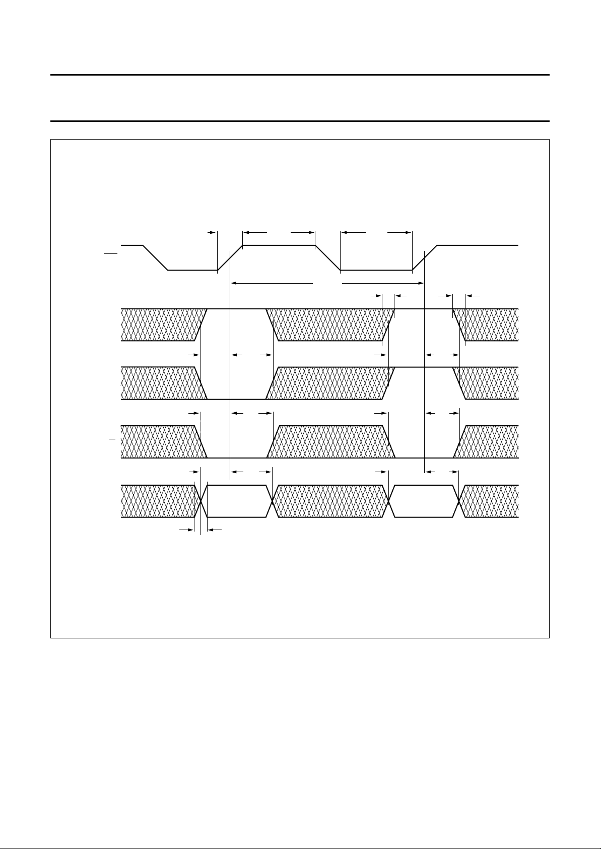
Philips Semiconductors Product specification
DVB compliant descrambler SAA7206H
handbook, full pagewidth
DCS
A1
A0
R/W
DAT0 to DAT7
t
r(CS)
t
su(i)
t
su(i)
t
su(i)
MSByte
t
i(r)
t
i(f)
t
CSH
t
h(i)
t
h(i)
t
h(i)
t
f(CS)
T
cy(CS)
t
CSL
t
i(r)
t
su(i)
t
su(i)
t
su(i)
LSByte
t
t
t
h(i)
h(i)
h(i)
t
i(f)
MGG326
Fig.14 Timing definition of the microcontroller interface signals (address write cycle).
1996 Oct 09 46
Page 47

Philips Semiconductors Product specification
DVB compliant descrambler SAA7206H
handbook, full pagewidth
DCS
A1
A0
R/W
DAT0 to DAT7
t
r(CS)
t
su(i)
t
su(i)
t
su(i)
MSByte
t
i(r)
t
i(f)
t
CSH
t
h(i)
t
h(i)
t
h(i)
t
f(CS)
T
cy(CS)
t
CSL
t
i(f)
t
su(i)
t
su(i)
t
su(i)
LSByte
t
t
t
h(i)
h(i)
h(i)
t
i(r)
MGG327
Fig.15 Timing definition of the microcontroller interface signals (data write cycle).
1996 Oct 09 47
Page 48

Philips Semiconductors Product specification
DVB compliant descrambler SAA7206H
handbook, full pagewidth
DCS
A1
A0
R/W
DATA
t
f(CS)
t
o(h)
t
CSLr
t
su(i)
t
o(h)
t
o(d)
t
o(d)
t
r(CS)
LSByteMSByte
t
h(i)
t
oL(Z)
Fig.16 Timing definition of the microcontroller interface signals (read cycle).
1996 Oct 09 48
t
o(r)
t
o(f)
t
oH(Z)
MGG328
Page 49

Philips Semiconductors Product specification
DVB compliant descrambler SAA7206H
13 PACKAGE OUTLINE
QFP64: plastic quad flat package; 64 leads (lead length 1.95 mm); body 14 x 20 x 2.8 mm
c
y
X
51 33
52
pin 1 index
64
1
32
Z
e
w M
b
p
20
19
A
E
A
H
E
2
A
E
A
1
detail X
SOT319-2
Q
L
p
L
(A )
3
θ
w M
b
e
p
Z
D
D
H
D
0 5 10 mm
scale
DIMENSIONS (mm are the original dimensions)
mm
A
max.
3.20
0.25
0.05
2.90
2.65
0.25
UNIT A1A2A3b
cE
p
0.50
0.25
0.35
0.14
(1)
(1) (1)(1)
D
20.1
19.9
eH
H
14.1
13.9
24.2
1
23.6
Note
1. Plastic or metal protrusions of 0.25 mm maximum per side are not included.
OUTLINE
VERSION
IEC JEDEC EIAJ
REFERENCES
SOT319-2
1996 Oct 09 49
D
B
v M
A
v M
B
LLpQZywv θ
E
18.2
17.6
1.0
0.6
1.4
1.2
0.2 0.10.21.95
EUROPEAN
PROJECTION
Z
D
1.2
1.2
0.8
0.8
ISSUE DATE
E
o
7
o
0
92-11-17
95-02-04
Page 50

Philips Semiconductors Product specification
DVB compliant descrambler SAA7206H
14 SOLDERING
14.1 Introduction
There is no soldering method that is ideal for all IC
packages. Wave soldering is often preferred when
through-hole and surface mounted components are mixed
on one printed-circuit board. However, wave soldering is
not always suitable for surface mounted ICs, or for
printed-circuits with high population densities. In these
situations reflow soldering is often used.
This text gives a very brief insight to a complex technology.
A more in-depth account of soldering ICs can be found in
our
“IC Package Databook”
14.2 Reflow soldering
Reflow soldering techniques are suitable for all QFP and
SO packages.
The choice of heating method may be influenced by larger
plastic QFP packages (44 leads, or more). If infrared or
vapour phase heating is used and the large packages are
not absolutely dry (less than 0.1% moisture content by
weight), vaporization of the small amount of moisture in
them can cause cracking of the plastic body. For more
information, refer to the Drypack chapter in our
Reference Manual”
Reflow soldering requires solder paste (a suspension of
fine solder particles, flux and binding agent) to be applied
to the printed-circuit board by screen printing, stencilling or
pressure-syringe dispensing before package placement.
Several techniques exist for reflowing; for example,
thermal conduction by heated belt. Dwell times vary
between 50 and 300 seconds depending on heating
method. Typical reflow temperatures range from
215 to 250 °C.
Preheating is necessary to dry the paste and evaporate
the binding agent. Preheating duration: 45 minutes at
45 °C.
(order code 9397 750 00192).
(order code 9398 652 90011).
“Quality
If wave soldering cannot be avoided, the following
conditions must be observed:
• A double-wave (a turbulent wave with high upward
pressure followed by a smooth laminar wave)
soldering technique should be used.
• The footprint must be at an angle of 45° to the board
direction and must incorporate solder thieves
downstream and at the side corners.
Even with these conditions, do not consider wave
soldering the following packages: QFP52 (SOT379-1),
QFP100 (SOT317-1), QFP100 (SOT317-2),
QFP100 (SOT382-1) or QFP160 (SOT322-1).
14.3.2 SO
Wave soldering techniques can be used for all SO
packages if the following conditions are observed:
• A double-wave (a turbulent wave with high upward
pressure followed by a smooth laminar wave) soldering
technique should be used.
• The longitudinal axis of the package footprint must be
parallel to the solder flow.
• The package footprint must incorporate solder thieves at
the downstream end.
14.3.3 M
During placement and before soldering, the package must
be fixed with a droplet of adhesive. The adhesive can be
applied by screen printing, pin transfer or syringe
dispensing. The package can be soldered after the
adhesive is cured.
Maximum permissible solder temperature is 260 °C, and
maximum duration of package immersion in solder is
10 seconds, if cooled to less than 150 °C within
6 seconds. Typical dwell time is 4 seconds at 250 °C.
A mildly-activated flux will eliminate the need for removal
of corrosive residues in most applications.
ETHOD (QFP AND SO)
14.3 Wave soldering
14.3.1 QFP
Wave soldering is not recommended for QFP packages.
This is because of the likelihood of solder bridging due to
closely-spaced leads and the possibility of incomplete
solder penetration in multi-lead devices.
1996 Oct 09 50
14.4 Repairing soldered joints
Fix the component by first soldering two diagonallyopposite end leads. Use only a low voltage soldering iron
(less than 24 V) applied to the flat part of the lead. Contact
time must be limited to 10 seconds at up to 300 °C. When
using a dedicated tool, all other leads can be soldered in
one operation within 2 to 5 seconds between
270 and 320 °C.
Page 51

Philips Semiconductors Product specification
DVB compliant descrambler SAA7206H
15 DEFINITIONS
Data sheet status
Objective specification This data sheet contains target or goal specifications for product development.
Preliminary specification This data sheet contains preliminary data; supplementary data may be published later.
Product specification This data sheet contains final product specifications.
Limiting values
Limiting values given are in accordance with the Absolute Maximum Rating System (IEC 134). Stress above one or
more of the limiting values may cause permanent damage to the device. These are stress ratings only and operation
of the device at these or at any other conditions above those given in the Characteristics sections of the specification
is not implied. Exposure to limiting values for extended periods may affect device reliability.
Application information
Where application information is given, it is advisory and does not form part of the specification.
16 LIFE SUPPORT APPLICATIONS
These products are not designed for use in life support appliances, devices, or systems where malfunction of these
products can reasonably be expected to result in personal injury. Philips customers using or selling these products for
use in such applications do so at their own risk and agree to fully indemnify Philips for any damages resulting from such
improper use or sale.
1996 Oct 09 51
Page 52

Philips Semiconductors – a worldwide company
Argentina: see South America
Australia: 34 Waterloo Road, NORTH RYDE, NSW 2113,
Tel. +61 2 9805 4455, Fax. +61 2 9805 4466
Austria: Computerstr. 6, A-1101 WIEN, P.O. Box 213,
Tel. +43 1 60 101, Fax. +43 1 60 101 1210
Belarus: Hotel Minsk Business Center, Bld. 3, r. 1211, Volodarski Str. 6,
220050 MINSK, Tel. +375 172 200 733, Fax. +375 172 200 773
Belgium: see The Netherlands
Brazil: seeSouth America
Bulgaria: Philips Bulgaria Ltd., Energoproject, 15thfloor,
51 James Bourchier Blvd., 1407 SOFIA,
Tel. +359 2 689 211, Fax. +359 2 689 102
Canada: PHILIPS SEMICONDUCTORS/COMPONENTS,
Tel. +1 800 234 7381
China/Hong Kong: 501 Hong Kong Industrial Technology Centre,
72 Tat Chee Avenue, Kowloon Tong, HONG KONG,
Tel. +852 2319 7888, Fax. +852 2319 7700
Colombia: see South America
Czech Republic: see Austria
Denmark: Prags Boulevard 80, PB 1919, DK-2300 COPENHAGEN S,
Tel. +45 32 88 2636, Fax. +45 31 57 1949
Finland: Sinikalliontie 3, FIN-02630 ESPOO,
Tel. +358 9 615800, Fax. +358 9 61580/xxx
France: 4 Rue du Port-aux-Vins, BP317, 92156 SURESNES Cedex,
Tel. +33 1 40 99 6161, Fax. +33 1 40 99 6427
Germany: Hammerbrookstraße 69, D-20097 HAMBURG,
Tel. +49 40 23 53 60, Fax. +49 40 23 536 300
Greece: No. 15, 25th March Street, GR 17778 TAVROS/ATHENS,
Tel. +30 1 4894 339/239, Fax. +30 1 4814 240
Hungary: seeAustria
India: Philips INDIA Ltd, Shivsagar Estate, A Block, Dr. Annie Besant Rd.
Worli, MUMBAI 400 018, Tel. +91 22 4938 541, Fax. +91 22 4938 722
Indonesia: see Singapore
Ireland: Newstead, Clonskeagh, DUBLIN 14,
Tel. +353 1 7640 000, Fax. +353 1 7640 200
Israel: RAPAC Electronics, 7 Kehilat Saloniki St, TEL AVIV 61180,
Tel. +972 3 645 0444, Fax. +972 3 649 1007
Italy: PHILIPS SEMICONDUCTORS, Piazza IV Novembre 3,
20124 MILANO, Tel. +39 2 6752 2531, Fax. +39 2 6752 2557
Japan: Philips Bldg 13-37, Kohnan 2-chome, Minato-ku, TOKYO 108,
Tel. +81 3 3740 5130, Fax. +81 3 3740 5077
Korea: Philips House, 260-199 Itaewon-dong, Yongsan-ku, SEOUL,
Tel. +82 2 709 1412, Fax. +82 2 709 1415
Malaysia: No. 76 Jalan Universiti, 46200 PETALING JAYA, SELANGOR,
Tel. +60 3 750 5214, Fax. +60 3 757 4880
Mexico: 5900 Gateway East, Suite 200, EL PASO, TEXAS 79905,
Tel. +9-5 800 234 7381
Middle East: see Italy
Netherlands: Postbus 90050, 5600 PB EINDHOVEN, Bldg. VB,
Tel. +31 40 27 82785, Fax. +31 40 27 88399
New Zealand: 2 Wagener Place, C.P.O. Box 1041, AUCKLAND,
Tel. +64 9 849 4160, Fax. +64 9 849 7811
Norway: Box 1, Manglerud 0612, OSLO,
Tel. +47 22 74 8000, Fax. +47 22 74 8341
Philippines: Philips Semiconductors Philippines Inc.,
106 Valero St. Salcedo Village, P.O. Box 2108 MCC, MAKATI,
Metro MANILA, Tel. +63 2 816 6380, Fax. +63 2 817 3474
Poland: Ul. Lukiska 10, PL 04-123 WARSZAWA,
Tel. +48 22 612 2831, Fax. +48 22 612 2327
Portugal: see Spain
Romania: see Italy
Russia: Philips Russia, Ul. Usatcheva 35A, 119048 MOSCOW,
Tel. +7 095 247 9145, Fax. +7 095 247 9144
Singapore: Lorong 1, Toa Payoh, SINGAPORE 1231,
Tel. +65 350 2538, Fax. +65 251 6500
Slovakia: see Austria
Slovenia: see Italy
South Africa: S.A. PHILIPS Pty Ltd., 195-215 Main Road Martindale,
2092 JOHANNESBURG, P.O. Box 7430 Johannesburg 2000,
Tel. +27 11 470 5911, Fax. +27 11 470 5494
South America: Rua do Rocio 220, 5th floor, Suite 51,
04552-903 São Paulo, SÃO PAULO - SP, Brazil,
Tel. +55 11 821 2333, Fax. +55 11 829 1849
Spain: Balmes 22, 08007 BARCELONA,
Tel. +34 3 301 6312, Fax. +34 3 301 4107
Sweden: Kottbygatan 7, Akalla, S-16485 STOCKHOLM,
Tel. +46 8 632 2000, Fax. +46 8 632 2745
Switzerland: Allmendstrasse 140, CH-8027 ZÜRICH,
Tel. +41 1 488 2686, Fax. +41 1 481 7730
Taiwan: PHILIPS TAIWAN Ltd., 23-30F, 66,
Chung Hsiao West Road, Sec. 1, P.O. Box 22978,
TAIPEI 100, Tel. +886 2 382 4443, Fax. +886 2 382 4444
Thailand: PHILIPS ELECTRONICS (THAILAND) Ltd.,
209/2 Sanpavuth-Bangna Road Prakanong, BANGKOK 10260,
Tel. +66 2 745 4090, Fax. +66 2 398 0793
Turkey: Talatpasa Cad. No. 5, 80640 GÜLTEPE/ISTANBUL,
Tel. +90 212 279 2770, Fax. +90 212 282 6707
Ukraine: PHILIPS UKRAINE, 4 Patrice Lumumba str., Building B, Floor 7,
252042 KIEV, Tel. +380 44 264 2776, Fax. +380 44 268 0461
United Kingdom: Philips Semiconductors Ltd., 276 Bath Road, Hayes,
MIDDLESEX UB3 5BX, Tel. +44 181 730 5000, Fax. +44 181 754 8421
United States: 811 East Arques Avenue, SUNNYVALE, CA 94088-3409,
Tel. +1 800 234 7381
Uruguay: see South America
Vietnam: see Singapore
Yugoslavia: PHILIPS, Trg N. Pasica 5/v, 11000 BEOGRAD,
Tel. +381 11 625 344, Fax.+381 11 635 777
For all other countries apply to: Philips Semiconductors, Marketing & Sales Communications,
Building BE-p, P.O. Box 218, 5600 MD EINDHOVEN, The Netherlands, Fax. +31 40 27 24825
© Philips Electronics N.V. 1996 SCA52
All rights are reserved. Reproduction in whole or in part is prohibited without the prior written consent of the copyright owner.
The information presented in this document does not form part of any quotation or contract, is believed to be accurate and reliable and may be changed
without notice. No liability will be accepted by the publisher for any consequence of its use. Publication thereof does not convey nor imply any license
under patent- or other industrial or intellectual property rights.
Internet: http://www.semiconductors.philips.com
Printed in The Netherlands 537021/1200/02/pp52 Date of release: 1996Oct 09 Document order number: 9397 750 01331
 Loading...