

Page 1

INTEGRATED CIRCUITS
DATA SH EET
SAA7205H
MPEG-2 systems demultiplexer
Preliminary specification
File under Integrated Circuits, IC02
1997 Jan 21
Page 2

Philips Semiconductors Preliminary specification
MPEG-2 systems demultiplexer SAA7205H
CONTENTS
1 FEATURES
2 GENERAL DESCRIPTION
3 QUICK REFERENCE DATA
4 ORDERING INFORMATION
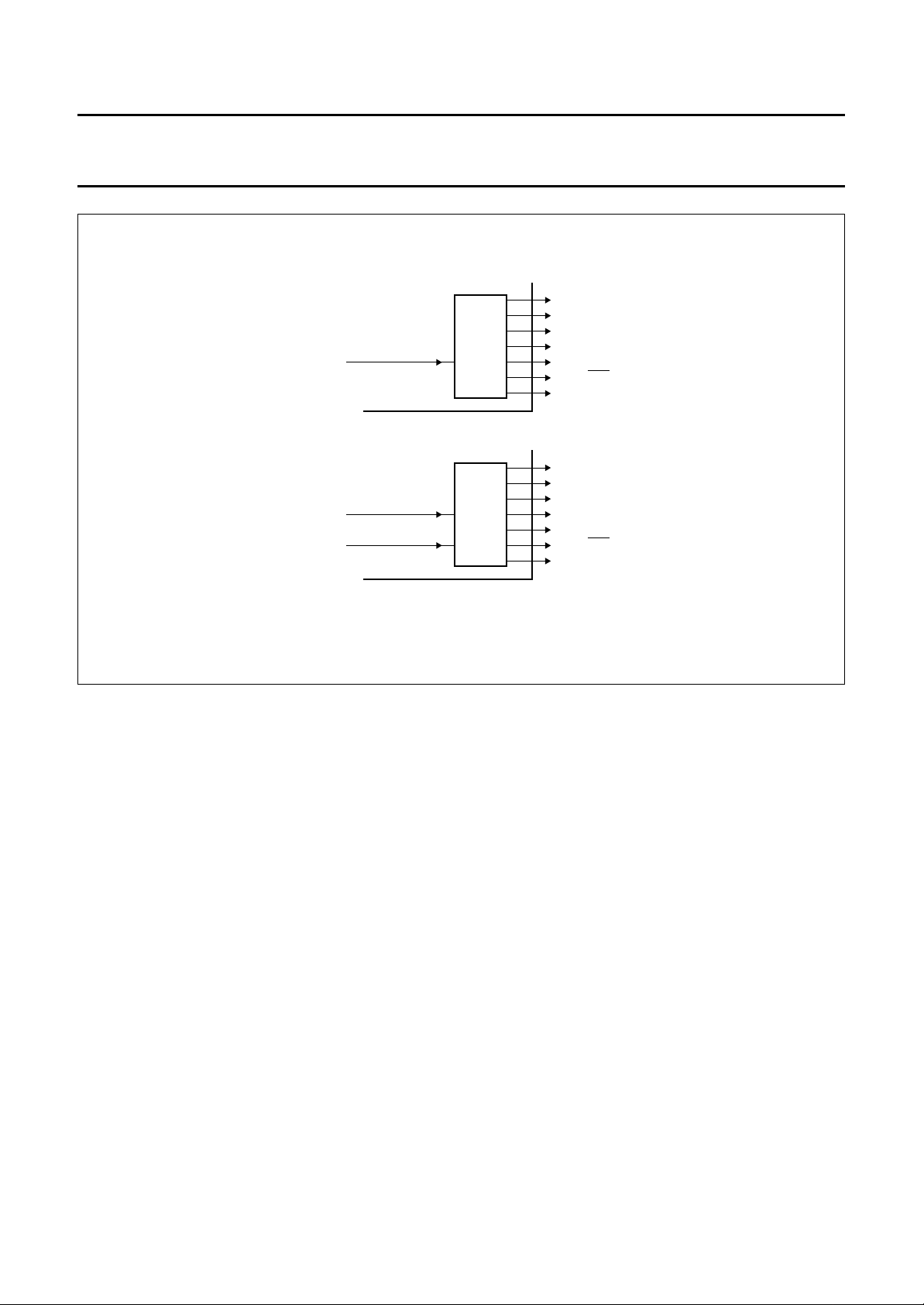
5 BLOCK DIAGRAM
6 PINNING
7 FUNCTIONAL DESCRIPTION
7.1 Functional overview
7.1.1 MPEG-2 syntax parser
7.1.2 Error handling
7.1.3 Teletext filter
7.1.4 Generic data filter
7.1.5 High speed data filter
7.1.6 Video data filter
7.1.7 Audio data filter
7.1.8 Program clock reference processor
7.1.9 Time stamp processors
7.1.10 FIFO buffers
7.1.11 Microcontroller interface
7.1.11.1 Short filters
7.1.11.2 Long filters
7.1.11.3 Subtitling filter
7.2 MPEG-2 systems parsing
7.3 Error handling
7.4 Interfacing to the external descrambler
7.5 High speed data interfacing
7.6 Interfacing to Philips SAA7201 video decoder
7.7 Interfacing to a third party video decoder
7.8 Interfacing to SAA2500 and third party audio
decoders
7.9 Interfacing to combined audio/video decoders
7.10 Interfacing to SAA9042 and SAA5270 teletext
decoders and SAA7183 EURO-DENC
7.11 Program clock reference processing
7.12 Time stamp processing (PTS/DTS)
7.13 Output buffering for audio and video
7.14 Microcontroller interfacing
7.14.1 Short filter module
7.14.2 Long filter module
7.14.3 Subtitling filter
8 PROGRAMMING THE DEMULTIPLEXER
9 LIMITING VALUES
10 HANDLING
11 DC CHARACTERISTICS
12 AC CHARACTERISTICS
13 APPENDIX
14 PACKAGE OUTLINE
15 SOLDERING
15.1 Introduction
15.2 Reflow soldering
15.3 Wave soldering
15.4 Repairing soldered joints
16 DEFINITIONS
17 LIFE SUPPORT APPLICATIONS
1997 Jan 21 2
Page 3

Philips Semiconductors Preliminary specification
MPEG-2 systems demultiplexer SAA7205H
1 FEATURES
• Input data fully compliant with the Transport Stream
(TS) definition of the MPEG-2 systems specification
(International Standard; November 1994)
• Input data signals: Forward Error Correction (FEC) or
descrambler interface
– modem data input bus (8-bit wide)
PKTDAT7 to PKTDAT0
– valid input data indicator (PKTDATV)
– erroneous packet indicator (PKTBAD/PKTBAD)
– first packet byte indicator (PKTSYNC)
– byte strobe signal [for the asynchronous mode only
(PKTBCLK)]
• The interface can be configured to either of two modes:
– asynchronous mode; PKTBCLK < 9 MHz, for
connection to a modem (e.g. FEC)
– synchronous mode; PKTBCLK is not used for
connection to an external descrambler operating at
9 MHz. The descrambler chip clock (9 MHz; 33%
duty cycle) is generated and output to the
demultiplexer.
The descrambler chip clock [DCLK (9 MHz, 33% duty
cycle)] is generated and output by the demultiplexer
• External memory; standard 32K × 8-bit static RAM.
Required typical access time ≤ 50 ns, write pulse width
) ≤ 35 ns.
(t
WP
• Effective bit rate: f
• Control Interface; 8-bit multiplexed data/address
(MDAT7 to MDAT0), memory mapped I/O (P90CE201
microcontroller parallel bus compatible), in combination
with two microcontroller interrupt signals (IRQ andNMI).
In addition, a number of address input pins
(MA9 to MA2) allow direct access to a selected set of
demultiplexer registers.
• Output ports:
Video; two alternative applications;
– third party video decoder compatible (master or slave
horizontal or vertical sync generation)
– Philips SAA7201 compatible (via general purpose
output)
≤ 72 MHz
bit
Audio; third party audio decoder, or Philips SAA2500
compatible
Audio/video; third party combined A/V decoder
compatible, (programmable)
Teletext; a Teletext Clock/Teletext Data (TTC/TTD)
based serial interface to selected teletext decoders
(e.g. SAA9042). Alternatively, this interface can be
programmed to provide data for Vertical Blanking
Interval (VBI) insertion of teletext data. The interface
therefore includes a teletext data request input (TTR).
In this mode, the interface is compatible with the
SAA7183 (EURO-DENC) TXT interface.
HS Data; high-speed data output, outputting entire
transport packets, packet payloads, PES packet
payloads, or sections (programmable) at byte clock
frequency (9 MHz). In the test mode it is capable of
outputting copies of either video, audio or other data
streams (programmable).
HS pins are combined with the general purpose
interface. The general purpose interface is bidirectional,
and can therefore, be used as an alternative transport
stream input.
• Descrambler; 8-bit wide data input interface, combined
with the modem input bus. A descrambler device may
output a descrambled transport stream at 9 MByte/s.
A 9 MHz descrambler clock is generated and output by
the demultiplexer.
• Microcontroller support; only for control, no specific
demultiplexing tasks are performed by the
microcontroller. However, parsing and processing of
Program Specific Information (PSI), and Service
Information (SI) is left to the microcontroller.
• Error handling; stream dependent error handling
algorithms, invoked either if the
signal is set, or if the transport_error_indicator bit
(MPEG-2 syntax) is set or if the parser detects an
MPEG-2 syntax error. Different handling algorithms are
applied for the various output ports.
PKTBAD/PKTBAD input
1997 Jan 21 3
Page 4
Philips Semiconductors Preliminary specification
MPEG-2 systems demultiplexer SAA7205H
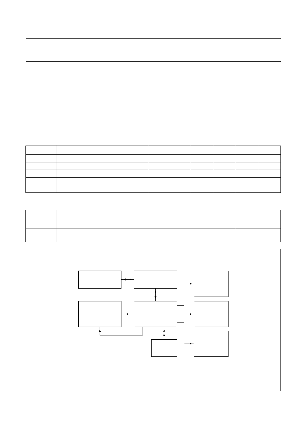
2 GENERAL DESCRIPTION
This document specifies the MPEG-2 systems demultiplexer IC, SAA7205H, for use in MPEG-2 based digital TV
receivers, possibly incorporating conditional access. Such receivers are to be implemented in, for instance, a Digital
Video Broadcasting (DVB) set-top box, or Integrated Receiver Decoder (IRD). An example of a
demultiplexer/descrambler system configuration, containing a channel decoder module, source decoders, a system
microcontroller and a conditional access system is shown in Fig.1. The main function of the demultiplexer is to separate
relevant data from an incoming MPEG-2 systems compliant data stream and pass it to both the individual source
decoders and to the system microcontroller. To support descrambling, the demultiplexer interfaces with the descrambler
part of a conditional access system (optional). The demultiplexer therefore generates a 9 MHz descrambler chip clock.
3 QUICK REFERENCE DATA
SYMBOL PARAMETER CONDITIONS MIN. TYP. MAX. UNIT
V
DDD
V
DDD(core)
P
tot
f
CLK
T
amb
digital supply voltage 4.5 5.0 5.5 V
digital supply voltage for core 3.0 3.3 3.6 V
total power consumption −−380 mW
clock frequency f
≤ 9 MHz −−27 MHz
byte
operating ambient temperature 0 − 70 °C
4 ORDERING INFORMATION
TYPE
NUMBER
NAME DESCRIPTION VERSION
PACKAGE
SAA7205H QFP128 plastic quad flat package; 128 leads (lead length 1.6 mm);
body 28 × 28 × 3.4 mm; high stand-off height
handbook, full pagewidth
CONDITIONAL
ACCESS
SYSTEM
DEMODULATOR PLUS
FORWARD ERROR
CORRECTOR
(AND DESCRAMBLER)
9 MHz DCLK
MICROCONTROLLER
SAA7205H
32K x 8
SRAM
DECODER
DECODER
TELETEXT
DECODER
SOT320-2
AUDIO
SOURCE
VIDEO
SOURCE
Fig.1 Demultiplexer system configuration.
1997 Jan 21 4
MGG374
Page 5
Philips Semiconductors Preliminary specification
MPEG-2 systems demultiplexer SAA7205H
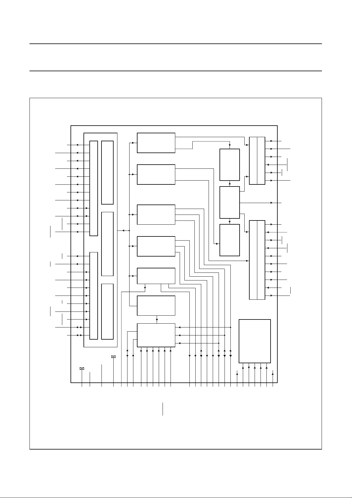
5 BLOCK DIAGRAM
MGG373
59
to
RAMA5
65,
RAMA8
75 71,
70
RAMA11
68
73
RAMA13
69
55
RAMIO0
74 49
WERAM
54
NMI
86 101 102
MA0
87
88
MA9
97
R/W
100 99 98
77
CSDEM
1
VO0
64
66
72
SUBTITLING/
PRIVATE FILTER
RAM INTERFACE
to
57
to
53
MODULE
LONG FILTER
to
95
DATA
AUDIO
FILTER
DATA
VIDEO
FILTER
DATA
FILTER
GENERIC
FILTER
H/S DATA
TXT
FILTER
DECODING
TIME STAMP
PROCESSOR
PRESENTATION/
REFERENCE
PROCESSOR
PROGRAM CLOCK
DECODING
TIME STAMP
PROCESSOR
PRESENTATION/
BUFFER
BUFFER
CONTROL
CONTROL
SAA7205H
ERROR
STREAM
TRANSPORT
HANDLING
AND
AF PARSER
FOR
TEST CONTROL BLOCK
BOUNDARY SCAN TEST
AND
SCAN TEST
MODULE
MICROCONTROLLER INTERFACE
to
84
to
8
SHORT FILTER
AUDAT
AUDATCLK
AUDATV
AUDATR
AUE
10 11 15 14 13 12
AUDECLK
33
COMSYNC PWMO
VSEL
CLKP
VREQ
CLK13.5
CbREF
HSYNC
VSYNC
VIN
40 47 42 43 45 46 128 127 104 44
EVEN/ODD
Fig.2 Block diagram.
to
RAMA0
RAMA7
RAMA6,
RAMA9,
RAMA10
RAMA12
RAMA14
to
RAMIO2
to
RAMIO3
RAMIO7
OERAM
handbook, full pagewidth
IRQ
MA1
to
MA2
MA10
CSVID
to
MDAT0
MDAT7
to
VO7
16, 85
SSD(core)
V
23, 76
9, 34, 41,
DDD(core)
V
32, 36, 48, 67,
105, 113, 126
58, 96, 120
DDD6
V
DDD1 to
V
37
SSD7
V
SSD1 to
V
24 to 31
TTR
109 to 112
118
119
DCLK
PKTBCLK
GPO7 to GPO0
114 to 117
PKTDAT7 to PKTDAT4
PKTDAT3 to PKTDAT0
107
108
106
PKTDATV
PKTSYNC
PKTBAD/PKTBAD
1997 Jan 21 5
38
39
TTD
TTC
171819
21
20
22
HSE
HSV
HSSYNC
GPV
GPST
35
CCLKI
GPSYNC
121
TC0/TDI
122
TDO
123
TMS
124
125
TRST
TC1/TCLK
103
POR
Page 6

Philips Semiconductors Preliminary specification
MPEG-2 systems demultiplexer SAA7205H
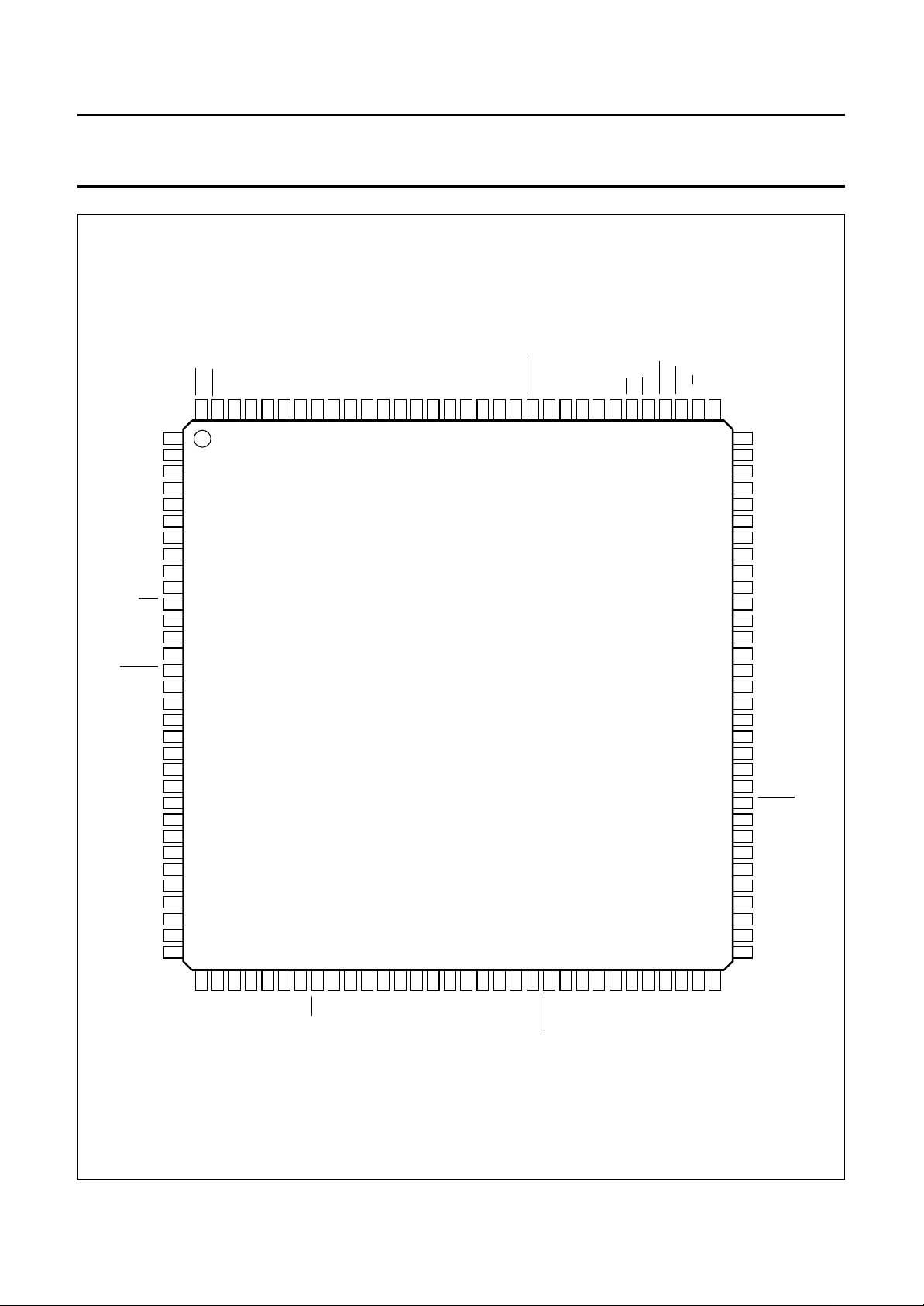
6 PINNING
SYMBOL PIN I/O DESCRIPTION
VO7 1 I/O data output bit 7 to video decoder (shared with microcontroller data)
VO6 2 I/O data output bit 6 to video decoder (shared with microcontroller data)
VO5 3 I/O data output bit 5 to video decoder (shared with microcontroller data)
VO4 4 I/O data output bit 4 to video decoder (shared with microcontroller data)
VO3 5 I/O data output bit 3 to video decoder (shared with microcontroller data)
VO2 6 I/O data output bit 2 to video decoder (shared with microcontroller data)
VO1 7 I/O data output bit 1 to video decoder (shared with microcontroller data)
VO0 8 I/O data output bit 0 to video decoder (shared with microcontroller data)
V
DDD1
AUDECLK 10 O audio decoder clock output [equals CCLKI/M (programmable)]
AUE 11 O audio data error indicator output (active LOW)
AUDAT 12 O data output to audio decoder (elementary stream)
AUDATCLK 13 O audio data clock output (frequency range 32 to 448 kHz; 9 Mbit/s)
AUDATV 14 O audio data valid indicator output
AUDATR 15 I audio data request input (active LOW)
V
SSD1(core)
GPV 17 I/O valid data byte indicator input/output
GPST 18 I/O byte strobe signal input/output (equals 9 MHz gated byte clock)
GPSYNC 19 I/O packet sync byte indicator input/output
HSE 20 I/O indicates erroneous HS data input/output
HSV 21 O valid high speed data indicator
HSSYNC 22 O indicates the first output byte of either a packet or payload
V
DDD1(core)
GPO7 24 I/O high speed byte output bit 7 for transport packets/general purpose byte output
GPO6 25 I/O high speed byte output bit 6 for transport packets/general purpose byte output
GPO5 26 I/O high speed byte output bit 5 for transport packets/general purpose byte output
GPO4 27 I/O high speed byte output bit 4 for transport packets/general purpose byte output
GPO3 28 I/O high speed byte output bit 3 for transport packets/general purpose byte output
GPO2 29 I/O high speed byte output bit 2 for transport packets/general purpose byte output
GPO1 30 I/O high speed byte output bit 1 for transport packets/general purpose byte output
GPO0 31 I/O high speed byte output bit 0 for transport packets/general purpose byte output
V
SSD1
PWMO 33 O pulse width modulated VCO control signal output (local STC)
9 supply digital supply voltage 1 (+5 V)
16 GND digital ground 1 for core
23 supply digital supply voltage 1 for core (+3.3 V)
(e.g. for SAA7201)/alternative transport stream input
(e.g. for SAA7201)/alternative transport stream input
(e.g. for SAA7201)/alternative transport stream input
(e.g. for SAA7201)/alternative transport stream input
(e.g. for SAA7201)/alternative transport stream input
(e.g. for SAA7201)/alternative transport stream input
(e.g. for SAA7201)/alternative transport stream input
(e.g. for SAA7201)/alternative transport stream input
32 GND digital ground 1
1997 Jan 21 6
Page 7

Philips Semiconductors Preliminary specification
MPEG-2 systems demultiplexer SAA7205H
SYMBOL PIN I/O DESCRIPTION
V
DDD2
CCLKI 35 I 27 MHz demultiplexer chip clock Input
V
SSD2
TTR 37 I teletext data request input (for VBI insertion of TXT)
TTD 38 O serial teletext data output (6.75 or 6.9375 Mbit/s)
TTC 39 O TXT clock (6.75 MHz = CCLKI/4)
ODD 40 O field parity output, internally generated, locked to COMSYNC
EVEN/
V
DDD3
VSYNC 42 O vertical sync output, locked to CCLKI and optionally VIN
HSYNC 43 O horizontal sync output, internally generated
COMSYNC 44 O (CCIR601) composite sync (50 and 60 Hz)
CbREF 45 O indicating U samples in UY and VY video decoder output
CLK13.5 46 O equals CCLKI/2
VIN 47 I receiver local vertical sync input, locked to CCLKI (optional)
V
SSD3
RAMIO3 49 I/O external SRAM input/output bus bit 3
RAMIO4 50 I/O external SRAM input/output bus bit 4
RAMIO5 51 I/O external SRAM input/output bus bit 5
RAMIO6 52 I/O external SRAM input/output bus bit 6
RAMIO7 53 I/O external SRAM input/output bus bit 7
OERAM 54 O output enable for external 32K × 8 SRAM (active LOW)
RAMIO2 55 I/O external SRAM input/output bus bit 2
RAMIO1 56 I/O external SRAM input/output bus bit 1
RAMIO0 57 I/O external SRAM input/output bus bit 0
V
DDD4
RAMA0 59 O external SRAM address bus output bit 0
RAMA1 60 O external SRAM address bus output bit 1
RAMA2 61 O external SRAM address bus output bit 2
RAMA3 62 O external SRAM address bus output bit 3
RAMA4 63 O external SRAM address bus output bit 4
RAMA5 64 O external SRAM address bus output bit 5
RAMA6 65 O external SRAM address bus output bit 6
RAMA7 66 O external SRAM address bus output bit 7
V
SSD4
RAMA12 68 O external SRAM address bus output bit 12
RAMA14 69 O external SRAM address bus output bit 14
RAMA11 70 O external SRAM address bus output bit 11
RAMA9 71 O external SRAM address bus output bit 9
RAMA8 72 O external SRAM address bus output bit 8
RAMA13 73 O external SRAM address bus output bit 13
WERAM 74 O write enable output for external SRAM (active LOW)
34 supply digital supply voltage 2 (+5 V)
36 GND digital ground 2
41 supply digital supply voltage 3 (+5 V)
48 GND digital ground 3
58 supply digital supply voltage 4 (+5 V)
67 GND digital ground 4
1997 Jan 21 7
Page 8

Philips Semiconductors Preliminary specification
MPEG-2 systems demultiplexer SAA7205H
SYMBOL PIN I/O DESCRIPTION
RAMA10 75 O external SRAM address bus output bit 10
V
DDD2(core)
MDAT0 77 I/O microcontroller bidirectional data bus bit 0
MDAT1 78 I/O microcontroller bidirectional data bus bit 1
MDAT2 79 I/O microcontroller bidirectional data bus bit 2
MDAT3 80 I/O microcontroller bidirectional data bus bit 3
MDAT4 81 I/O microcontroller bidirectional data bus bit 4
MDAT5 82 I/O microcontroller bidirectional data bus bit 5
MDAT6 83 I/O microcontroller bidirectional data bus bit 6
MDAT7 84 I/O microcontroller bidirectional data bus bit 7
V
SSD2(core)
MA0 86 I microcontroller MSByte/
MA1 87 I microcontroller address/
MA2 88 I microcontroller address input bit 2 for direct access to selected registers
MA3 89 I microcontroller address input bit 3 for direct access to selected registers
MA4 90 I microcontroller address input bit 4 for direct access to selected registers
MA5 91 I microcontroller address input bit 5 for direct access to selected registers
MA6 92 I microcontroller address input bit 6 for direct access to selected registers
MA7 93 I microcontroller address input bit 7 for direct access to selected registers
MA8 94 I microcontroller address input bit 8 for direct access to selected registers
MA9 95 I microcontroller address input bit 9 for direct access to selected registers
V
DDD5
MA10 97 I microcontroller direct addressing/indirect addressing indicator input bit 10
W 98 I read/write input selection
R/
CSVID 99 I (audio)/video decoder chip select input (active LOW)
CSDEM 100 I demultiplexer chip select input (active LOW)
IRQ 101 O interrupt request output for microcontroller (active LOW, open-drain)
NMI 102 O non-maskable interrupt output for VOUT bus access handling (open-drain)
POR 103 I power-on reset input
VSEL 104 I video input select signal (bus control by microcontroller)
V
SSD5
PKTSYNC 106 I indicates the first input byte (sync) of a transport packet
PKTDATV 107 I valid input data indicator
PKTBAD/
PKTBAD
PKTDAT7 109 I 8-bit wide modem data input bit 7
PKTDAT6 110 I 8-bit wide modem data input bit 6
PKTDAT5 111 I 8-bit wide modem data input bit 5
PKTDAT4 112 I 8-bit wide modem data input bit 4
V
SSD6
PKTDAT3 114 I 8-bit wide modem data input bit 3
76 supply digital supply voltage 2 for core (+3.3 V)
85 GND digital ground 2 for core
LSByte indicator input bit 0
data indicator input bit 1
96 supply digital supply voltage 5 (+5 V)
105 GND digital ground 5
108 I packet error indicator input (programmable polarity)
113 GND digital ground 6
1997 Jan 21 8
Page 9

Philips Semiconductors Preliminary specification
MPEG-2 systems demultiplexer SAA7205H
SYMBOL PIN I/O DESCRIPTION
PKTDAT2 115 I 8-bit wide modem data input bit 2
PKTDAT1 116 I 8-bit wide modem data input bit 1
PKTDAT0 117 I 8-bit wide modem data input bit 0
PKTBCLK 118 I byte strobe input signal (< 9 MHz)
DCLK 119 O 9 MHz descrambler chip clock output (33% duty cycle)
V
DDD6
TC0/TDI 121 I scan test data input/boundary scan test data input
TDO 122 O boundary scan test data output
TMS 123 I boundary scan test input mode select
TC1/TCLK 124 I scan test clock input/ boundary scan test clock input
TRST 125 I boundary scan test reset input (LOW in normal operation)
V
SSD7
CLKP 127 O gated clock output signal indicating valid data (9 MHz = CCLKI/3; active LOW)
VREQ 128 I video data request input (active LOW)
120 supply digital supply voltage 6 (+5 V)
126 GND digital ground 7
1997 Jan 21 9
Page 10
Philips Semiconductors Preliminary specification
MPEG-2 systems demultiplexer SAA7205H
handbook, full pagewidth
VO7
1
VO6
2
3
VO5
4
VO4
5
VO3
6
VO2
7
VO1
VO0
8
V
9
DDD1
AUE
AUDAT
AUDATV
AUDATR
GPV
GPST
HSE
HSV
GPO7
GPO6
GPO5
GPO4
GPO3
GPO2
GPO1
GPO0
V
SSD1
10
11
12
13
14
15
16
17
18
19
20
21
22
23
24
25
26
27
28
29
30
31
32
AUDECLK
AUDATCLK
V
SSD1(core)
GPSYNC
HSSYNC
V
DDD1(core)
VREQ
128
CLKP
127
SSD7
V
126
TRST
125
TC1/TCLK
TMS
TDO
122
124
123
DDD6
TC0/TDI
V
121
120
DCLK
119
PKTBCLK
PKTDAT0
118
117
PKTDAT1
116
PKTDAT2
115
SSD6
PKTDAT3
V
PKTDAT4
114
112
113
SAA7205H
PKTDAT5
111
PKTDAT6
PKTDAT7
PKTBAD/PKTBAD
110
109
108
PKTDATV
PKTSYNC
107
106
SSD5
V
105
VSEL
104
POR
103
NMI
102
IRQ
101
CSDEM
CSVID
999897
100
R/W
MA10
96
95
94
93
92
91
90
89
88
87
86
85
84
83
82
81
80
79
78
77
76
75
74
73
72
71
70
69
68
67
66
65
V
DDD5
MA9
MA8
MA7
MA6
MA5
MA4
MA3
MA2
MA1
MA0
V
SSD2(core)
MDAT7
MDAT6
MDAT5
MDAT4
MDAT3
MDAT2
MDAT1
MDAT0
V
DDD2(core)
RAMA10
WERAM
RAMA13
RAMA8
RAMA9
RAMA11
RAMA14
RAMA12
V
SSD4
RAMA7
RAMA6
3334353637
SSD2
DDD2
CCLKI
PWMO
V
V
39404142434445464748495051525354555657585960616263
38
TTR
TTD
TTC
EVEN/ODD
DDD3
V
VSYNC
HSYNC
COMSYNC
CbREF
CLK13.5
VIN
SSD3
V
Fig.3 Pin configuration.
1997 Jan 21 10
RAMIO3
RAMIO4
RAMIO5
RAMIO6
OERAM
RAMIO7
RAMIO2
RAMIO1
DDD4
V
RAMIO0
RAMA0
RAMA1
RAMA2
RAMA3
64
RAMA4
RAMA5
MGG372
Page 11

Philips Semiconductors Preliminary specification
MPEG-2 systems demultiplexer SAA7205H
7 FUNCTIONAL DESCRIPTION
7.1 Functional overview
A schematic diagram of the internal structure of the
MPEG-2 demultiplexer is shown in Fig.2. The diagram
illustrates the main functional entities in the demultiplexer.
7.1.1 MPEG-2
SYNTAX PARSER
The MPEG-2 syntax parser, parsing transport streams
which comply with the MPEG-2 systems specification
(International Standard, November 1994).
7.1.2 E
RROR HANDLING
Error handling is invoked whenever an error is detected.
Error handling is started on the basis of either the
PKTBAD/PKTBAD input signal (driven by the FEC
decoder), or the transport_error_indicator in the transport
packet header, or discovery of a syntax error by the parser.
7.1.3 T
ELETEXT FILTER
A teletext (TXT) filter, generating a teletext clock
(TTC = 6.75 MHz, derived from the chip clock,
CCLKI = 27 MHz) and providing a serial TXT data stream
(TTD) locked to both TTC and the horizontal video sync
(HSYNC) generated by the demultiplexer. In accordance
with the DVB specification, TXT data is transported in
MPEG-2 PES packets. The incoming transport stream is
filtered on the basis of a Programmable Packet
Identification (PID) and elementary stream data is stored
in a 2 kbyte FIFO buffer. Data is read from the TXT buffer
at 6.75 Mbit/s.
The TXT filter can, alternatively, be programmed to a
mode in which it provides TXT bits at 6.9375 MHz, on the
basis of an external request (TTR). This mode is applied
for vertical blanking interval insertion of TXT data. It is
compatible with the TXT input of the EURO-DENC
(SAA7183).
7.1.4 G
ENERIC DATA FILTER
A generic data filter is connected to the generic interface.
This filter in fact does not filter, but passes the entire
transport stream in byte format. A byte strobe signal
(GPST), indicating consecutive valid bytes, a valid signal
(GPV) and a header sync byte indicator (GPSYNC) are
generated.
Alternatively the general purpose interface can be
configured to function as transport stream input
(GP_Direction = 1; address 0x0700; see Table 13).
7.1.5 H
IGH SPEED DATA FILTER
A high speed data filter (HS), retrieves the entire transport
packets, packet payloads, PES payloads or sections from
the input stream on the basis of a programmable filter.
Data is output at the byte clock frequency
(DCLK = 9 MHz = CCLKI/3, 33% duty cycle). Selected
parts of a data stream are indicated by the HSV signal.
The first byte of a data entity is indicated by HSSYNC. The
HS filter shares its data output pins with the generic data
filter.
It should be noted that in the event that the HS filter is
programmed to the section mode, the GP bus only outputs
selected sections and not an entire transport stream.
7.1.6 V
IDEO DATA FILTER
A video data filter, with a decoder specific interface. This
filter selects either Packetized Elementary Stream (PES)
data, or Elementary Stream (ES) data (programmable) on
the basis of a programmable PID, and passes it to the
video FIFO. Presentation Time Stamps and Decoding
Time Stamps (PTS and DTS) are obtained from the PES
stream and can be read by the microcontroller (optional).
Video PES or ES data is output at 9 MHz, via a
bidirectional 8-bit wide bus which is time-shared with the
microcontroller. Access to the output bus is controlled by
the microcontroller using the VSEL signal.
The demultiplexer therefore, halts output video data
whenever VSEL = 0 and creates a bidirectional
communication link between the microcontroller and the
video decoder.
7.1.7 A
UDIO DATA FILTER
An audio data filter with a decoder specific interface. This
filter selects PES or ES data (programmable) on the basis
of a programmable PID and passes it to the audio FIFO.
Time-stamps are retrieved from audio PES headers and
can be read by the microcontroller (optional).
The audio filter can be switched to a mode in which the
microcontroller controls audio and video synchronization
(software sync). In this mode the filter outputs audio data
at 9 Mbit/s. The filter is also capable of handling
synchronization independently from the microcontroller.
In this situation the audio elementary stream output is
(hardware) synchronized to the System Time Clock (STC)
automatically. In the hardware synchronization mode, the
audio elementary stream data is output via a bit serial data
link at a bit rate between 32 to 448 kbit/s. The actual bit
rate depends on the type of audio frame that is handled
(as specified in the MPEG-2 audio specification).
1997 Jan 21 11
Page 12

Philips Semiconductors Preliminary specification
MPEG-2 systems demultiplexer SAA7205H
It should be noted that audio and video data can be
optionally combined on the output bus to interface to
combined audio/video decoders. In this mode the video
bus is controlled by the VSEL signal, an audio request
signal (AUDATR) and a video request signal (VREQ;
optional). Video and audio bytes are output at 9 MBytes
and are interleaved with a programmable audio/video
ratio.
7.1.8 P
ROGRAM CLOCK REFERENCE PROCESSOR
The PCR processor is capable of regenerating a local
system time clock. This block contains a digital clock
recovery loop. Two local clock counters generate an
absolute timing value (cycle time approximately 24 hours),
which is used to verify the phase relationship between the
local system time clock and the transmitter reference clock
(Program Clock Reference, or PCR). Two STC counters
are implemented to allow for correct handling of PCR
discontinuations.
7.1.9 T
IME STAMP PROCESSORS
These two PTS/DTS processors are capable of
synchronizing attached source decoders. The PTS/DTS
processors retrieve time stamps from the incoming
transport stream. They also compare emulated time
stamps (PTS/DTS) with the local absolute time value
generated by the PCR processor. In the event of equality
a microcontroller interrupt is generated.
The microcontroller can respond to this pulse by
instructing the attached source decoders to start decoding,
or to start presentation. For audio, the PTS values are
stored in the audio FIFO to be used for synchronization of
the FIFO output stream (called lip-sync).
7.1.10 FIFO
BUFFERS
There are two FIFO buffers for audio and video (6 kBytes
and 768 Bytes respectively), including buffer control, to
interface between different clock systems. These FIFOs
are filled at byte clock (CCLKI/3) frequency and emptied
on the acquisition clocks of the respective source
decoders [9 MByte/s for video and combined audio/video,
and a frequency in the range 32 to 448 kbit/s (hardware
sync), or 9 Mbit/s (software sync) for audio].
7.1.11 M
ICROCONTROLLER INTERFACE
The microcontroller interface provides protocol handling
for the memory mapped I/O control bus (Philips
P90CE201 compatible). This module also contains an
interrupt request handler and data filters for retrieval of
Program Specific Information (PSI), service information
(SI), Electronic Program Guides (EPG) (private sections),
subtitling (private sections) and low speed (LS) data
(private).
7.1.11.1 Short filters
The short filters select data on the basis of PIDs and a
combination of MPEG-2 section addressing fields.
Selected data is stored in twelve 1 kByte (constrained
random access) buffers. These buffers are located in the
external SRAM memory and can be read by the
microcontroller. The short filters are capable of monitoring
12 section streams simultaneously.
7.1.11.2 Long filters
The long filters also select data on the basis of PIDs and a
combination of MPEG-2 section addressing fields.
Selected data is stored in four 4 kByte (constrained
random access) buffers. These buffers are located in the
external SRAM memory and can be read by the
microcontroller. The long filters are capable of monitoring
4 section streams simultaneously.
7.1.11.3 Subtitling filter
The subtitling filter is capable of retrieving transport packet
payloads or PES payloads from the input stream, on the
basis of a programmable filter. It is also capable of
retrieving adaptation field and PES header private data.
Data is stored in a 4 kByte FIFO which is located in the
external SRAM memory and can be read by the
microcontroller.
Table 1 Filter types
FILTER TYPE NUMBER OF FILTERS BUFFER SIZE REMARKS
Short (sections) 12 12 × 1 kByte −
Long (sections) 4 4 × 4 kByte −
Subtitling 1 1 × 4 kByte PES and PES payload (ES), adaption field
private data, PES header private data
1997 Jan 21 12
Page 13

Philips Semiconductors Preliminary specification
MPEG-2 systems demultiplexer SAA7205H
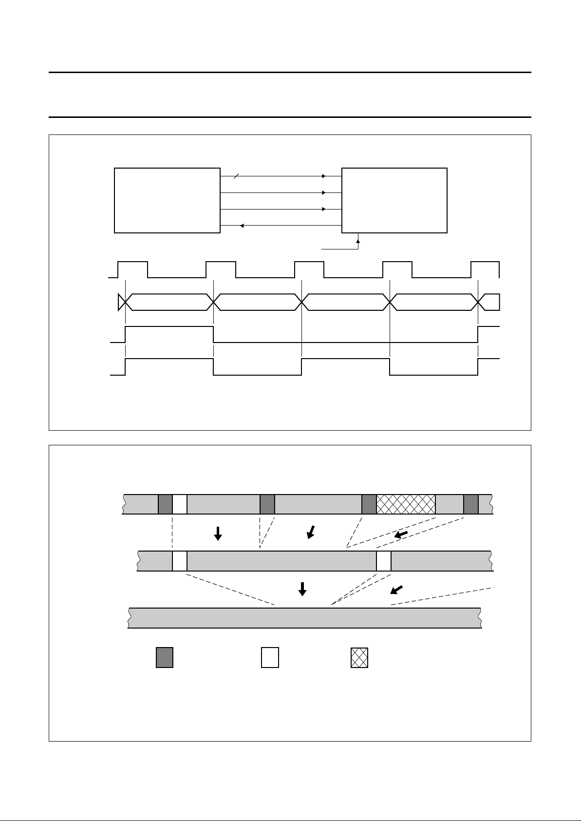
7.2 MPEG-2 systems parsing
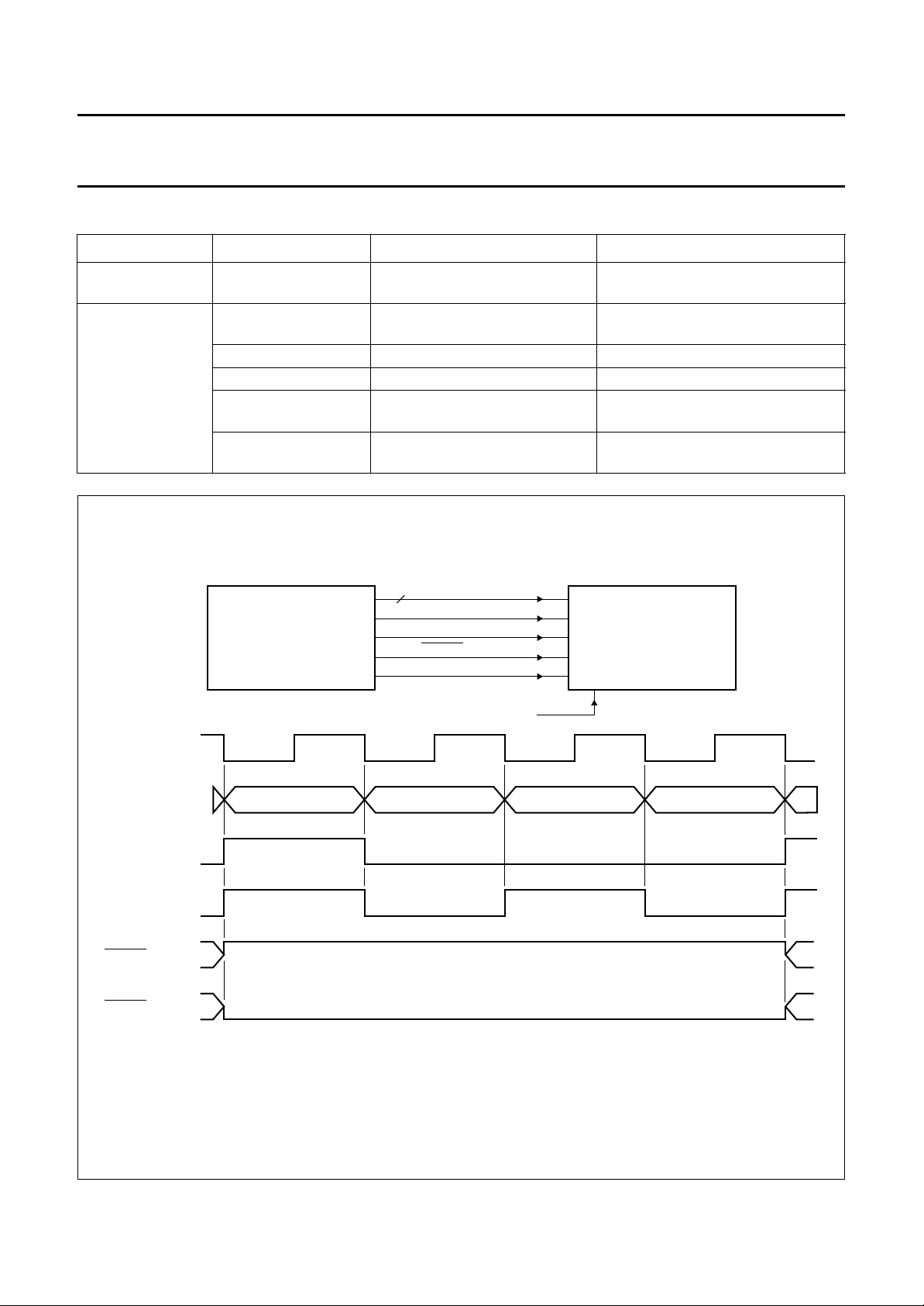
The demultiplexer receives data from a Forward Error
Correction (FEC) decoder (see Fig.4) or a descrambler
(see Fig.5) in a digital TV receiver in the following input
data format:
• A number of data bits via PKTDAT7 to PKTDAT0
(8-bit wide input bus)
• A valid input data indicator signal (PKTDATV) which is
HIGH for consecutive valid bytes and output by either a
FEC decoder or a descrambler. The demultiplexer input
is allowed to have a ‘bursty’ nature.
• A transport packet error indicator (
which is HIGH for the duration of each 188 byte
transport packet in which the FEC decoder found more
errors than it could correct. The polarity (active HIGH or
LOW) of the error indicator is programmable
(bit Bad_polarity, address 0x0100; see Table 13).
• A packet sync signal (PKTSYNC) which goes HIGH at
the start of the first byte of a transport packet. Only the
rising edge of PKTSYNC is used for synchronization,
the exact HIGH time of the signal is therefore irrelevant.
• A byte strobe signal [PKTBCLK (< 9 MHz)] which
indicates consecutive data bytes in the input stream, in
the non-9 MHz mode only (bit 9 MHz_interface = 0,
address 0x0100;see Table 13). PKTBCLK is used as an
enable signal and transport stream input bytes are
sampled on its rising edges of the clock pulse. If the
input interface is programmed to the 9 MHz mode
(9 MHz interface = 1), the PKTBCLK signal is ignored.
• A descrambler clock signal [DCLK (9 MHz, 30% duty
cycle)] which is the data output clock for the
descrambler. If rising edges of this clock signal are used
to input data to the demultiplexer the 9 MHz mode must
be used (bit 9 MHz_interface = 1, address 0x0100;
see Table 13).
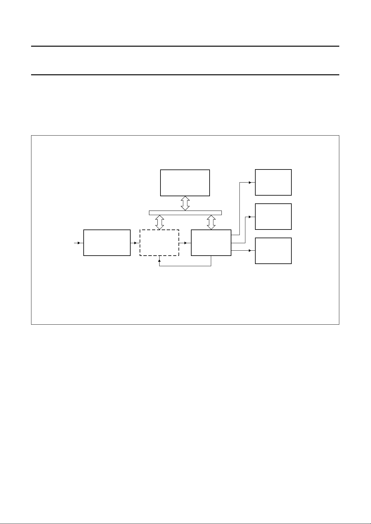
The parser module in the demultiplexer parses MPEG-2
systems compliant transport streams. MPEG-2 systems
specifies a hierarchical two level multiplex (see Fig.6).
The top hierarchical level is the transport stream,
consisting of relatively short (188 byte) transport packets.
Each transport packet consists of a 4 byte transport
header, an optional adaptation field and a payload.
PKTBAD/PKTBAD)
The transport header contains a 13-bit packet
identification field. The adaptation field may contain
Program Clock Reference (PCR) data and transport
private data, among others. Both the transport header and
the optional adaptation fields are parsed by the parser
module within the demultiplexer. The individual states of
the MPEG-2 parser in the demultiplexer are listed in
Table 14.
The hierarchical multiplex level below the MPEG-2
transport stream and the packetized elementary stream, is
partly parsed by the demultiplexer, for instance in the
audio and video filters. A packetized elementary stream
consists of an elementary stream (e.g. MPEG-2 audio, or
video data) which is divided into subsequent variable
section lengths. To each section a PES header is added,
thus creating PES packets. A PES header may contain
time stamp information (PTS or DTS), scrambling control,
copy information and PES private data.
In the demultiplexer, parsing is performed for all incoming
transport packets. The parser is synchronized to a rising
edge on the PKTSYNC input. A microcontroller can
compose a set of PIDs by programming the appropriate
registers in the various filters within the demultiplexer. If a
packet is part of an audio or video transport stream, some
of the information fields in the transport and PES packet
headers are automatically retrieved. The microcontroller
can read the obtained information. Table 2 lists data that
can be accessed by the microcontroller, for both video
(address 0x0509; see Table 13) and audio streams
(address 0x0609; see Table 13).
MPEG-2 multiplex fields which are related to program
specific information (PSI), service information (SI), private
data and conditional access data (called sections) are
parsed partly in the section data filters. Program
association tables, program map tables and conditional
access tables can be retrieved from the stream and stored
in buffers in an external 32K × 8 SRAM. The same can be
performed (optional) for transport_private_data,
PES_private_data, and private sections in the subtitling
and section data filters. A microcontroller may access data
in the section data and subtitling buffers for further
processing in software.
1997 Jan 21 13
Page 14
Philips Semiconductors Preliminary specification
MPEG-2 systems demultiplexer SAA7205H
Table 2 Microcontroller accessible MPEG-2 systems information
POSITION NUMBER OF BITS FIELD NAME FUNCTION
Transport packet
header
PES header 2 PES_scrambling_control
2 transport_scrambling_control
(bits: ts_scr_ctrl1 and 0)
indicates whether the associated bit
stream is scrambled or not
indicates whether the associated
(bits: pes_scr_ctrl1 and 0)
PES payload is scrambled or not
1 copyright (bit: cp_info1) anticopy management
1 original_or_copy (bit: cp_info0) anticopy management
1 additional_copy_info_flag
anticopy management
(bit: ad_cp_flag)
7 additional_copy_info
anticopy management
(bits: ad_cp_info7 to 0)
handbook, full pagewidth
PKTBCLK
PKTDAT7
PKTDAT0
PKTSYNC
PKTDATV
PKTBAD/PKTBAD
PKTBAD/PKTBAD
8
PKTDAT7 to PKTDAT0
FORWARD
ERROR
CORRECTOR
to
message invalid data
error-free transport packet (programmable polarity)
PKTBCLK
PKTDATV
PKTBAD/PKTBAD
PKTSYNC
erroneous transport packet
DEMULTIPLEXER
CCLKI
message invalid data
MGG375
Fig.4 Signal constellation FEC decoder - demultiplexer interfacing.
1997 Jan 21 14
Page 15
Philips Semiconductors Preliminary specification
MPEG-2 systems demultiplexer SAA7205H
8
handbook, full pagewidth
DESCRAMBLER
DCLK
PKTDAT7 to PKTDAT0
PKTDATV
PKTSYNC
DCLK
DEMULTIPLEXER
CCLKI
PKTDAT7
to
PKTDAT0
PKTSYNC
PKTDATV
handbook, full pagewidth
transport
stream
packetized
elementary
stream
message invalid data
message
Fig.5 Signal constellation descrambler - demultiplexer interfacing.
invalid data
MGG376
elementary
stream
= transport_header = pes_header = stuffing
Fig.6 MPEG-2 two level hierarchical demultiplexing.
1997 Jan 21 15
MGG318
Page 16

Philips Semiconductors Preliminary specification
MPEG-2 systems demultiplexer SAA7205H
7.3 Error handling
The error handling module responds to four situations in
which errors are present in the incoming stream:
• An erroneous packet is signalled to the demultiplexer,
by means of the PKTBAD/PKTBAD input signal.
The FEC decoder drives this signal LOW (or HIGH)
should it discovers that the number of errors in a packet
exceeds its correction capability. The polarity of the
PKTBAD/PKTBAD input signal is programmable
(bit Bad_pol, address 0x0100; see Table 13).
• The transport_error_indicator bit in the transport packet
header is set (equals logic 1), indicating that an error
occurred prior to, or during transmission
• A continuity counter discontinuity is detected
• The parser detects a syntax error in a packet, or is out
of sync.
In the first two cases, the transport_error_indicator bit in
the transport packet header is set. In all cases error
handling depends on the data stream the packet belongs
to, as indicated in Table 3. Most of the functions in this
table are executed in the data filters, not in the error
handling module. Error handling is therefore implemented
as a distributed function.
If the parser detects a syntax error or is out of sync, the
error handling module discards all incoming data, and an
interrupt is set (bit prs_sync_lost, address 0x0000,
see Table 13).
The error handling module keeps track of an average error
count. The module counts every occurrence of both
PKTBAD = 0 (or PKTBAD = 1) and
“transport_error_indicator = 1. The 16-bit error count value
can be read by the microcontroller, which can also reset
the counter every once in a while by writing all zeroes
(00..00) to the register (word cnt15 to cnt0], address
0x0200; see Table 13). The microcontroller can thus
determine an average packet error rate.
Table 3 Error handling algorithms
DATA STREAM OPTION ERROR HANDLING
Video third party decoder erroneous transport packets are discarded, no error flag is set, but a
sequence_error_code (0x000001B4) is inserted, whenever a
continuity_counter discontinuity is discovered
SAA7201 handling is altogether done in the SAA7201 source decoder
Audio − discard erroneous packets
TXT − discard erroneous packets
Subtitling − PES packet data are passed to the microcontroller. The error handling
decision is left to the microcontroller.
High speed
data
Section data − CRC calculation is performed in the filters. If an error is detected, an error flag
− programmable error handling (see Section “High speed data interfacing”)
(bit err_stat, address 0x0305 to 0x0314, see Table 13) is set. The error
handling decision is left to the microcontroller.
1997 Jan 21 16
Page 17
Philips Semiconductors Preliminary specification
MPEG-2 systems demultiplexer SAA7205H
7.4 Interfacing to the external descrambler
An optional external descrambler can be incorporated in a digital TV receiver in the configuration indicated in Fig.7.
In such a configuration the demultiplexer generates a 9 MHz, 33% duty cycle descrambler clock (DCLK) signal
(see Fig.5). A descrambler could use this clock signal for data processing and outputting data. In such a configuration
the demultiplexer input interface is set to 9 MHz mode (bit 9 MHz_interface = 1, address 0x0100, see Table 13).
handbook, full pagewidth
SYSTEM
MICROCONTROLLER
VIDEO
DECODER
AUDIO
DECODER
DEMODULATOR
AND
FORWARD ERROR
CORRECTOR
OPTIONAL
DESCRAMBLER
DCLK (9 MHz)
MPEG2
DEMULTIPLEXER
SAA7205H
Fig.7 Digital TV receiver configuration including a descrambler.
TELETEXT
AND
H/S DATA
APPLICATIONS
MGG767
1997 Jan 21 17
Page 18

Philips Semiconductors Preliminary specification
MPEG-2 systems demultiplexer SAA7205H
7.5 High speed data interfacing
The High Speed (HS) data filter module retrieves entire
transport packets, packet payloads, PES payloads, or
sections from the input stream, on the basis of a
programmable filter. The packets may contain data for
specific high speed data applications. In test mode
however, by reprogramming the filter
(word HS_pid12 to HS_pid0, address 0x0700;
see Table 13), data of other filters can be output. This
enables the user to monitor data streams directed to audio,
video, section data, and other filters. The HS data filter
features a programmable error handling mechanism. If the
‘HS_err_rmv’ (address 0x0701;see Table 13) bit is set,
erroneous output packets are removed from the stream.
If ‘HS_dupl_rmv’ (address 0x0701, see Table 13) is set,
the same is true for duplicate packets. Both removal
options can also be disabled.
In the single PID mode, the HS filter can be programmed
to operate in one of four filter modes (bits HS_mode,
address 0x0700, see Table 13), as indicated in Table 4.
Table 4 HS programmable filtering modes
OPERATING
MODE
Single PID
mode
Single PID
mode
(continued)
Multiple PID
mode
‘1 1..11’, indicating all PID
bits are relevant,
therefore only one
particular PID matches
‘1 1..11’, indicating all PID
bits are relevant,
therefore only one
particular PID matches
‘..0..1..’, indicating one or
more PID bits are don’t
care, so multiple PIDs
may match
PID MASK
(ADDRESS 0X0701;
see Table 13
FILTERING
OPTION
total TS packet outputs entire transport packets.
TS packet
payload
PES packet
payload
section outputs entire sections, based on
total TS packet output packet payloads only.
In multiple PID mode, only entire transport packets can be
output, for packets matching the PID specification.
Selected stream data is output (unbuffered) via the
GPO7 to GPO0 bus, at byte clock (DCLK) frequency
(rate = 9 MByte/s). Data is output in the format indicated in
Fig.8. The DCLK signal is a continuous byte clock.
The HSV signal is set for matching data only, otherwise it
is kept low. The HSSYNC signal indicates the position of
the first byte of the selected data, as indicated in Table 4.
Erroneous data is signalled by means of the HSE signal,
which is high for the duration of the erroneous packet.
In section mode HS data is selected on the basis of
table_id, and two section header bytes following the
section_length indicator (see Fig.26). For this purpose,
programmable filter masks are provided (address
0x0702 to 0x0704, see Table 13). If section mode is
selected, the general purpose output GPO7 to GPO0 does
not carry the full transport stream. Only selected sections
are output
FUNCTION HSSYNC
first byte of transport
(HS_mode = 00,
address 0x0700, see Table 13)
outputs transport packet
payloads for a selected PID.
(HS_mode = 01)
output PES packet payloads for a
selected PID. (HS_mode = 10)
PID, and table_id + 2 bytes
selection (addresses 0x0702 to
0x0704, see Table 13).
(HS_mode = 11 and
HS_sect_flt_en = 1)
(HS_mode = 00)
packet
first byte of transport
packet payload, only
if payload_unit_
start_indicator is set
first byte of PES
packet payload
first byte of section
header
first byte of transport
packet
1997 Jan 21 18
Page 19
Philips Semiconductors Preliminary specification
MPEG-2 systems demultiplexer SAA7205H
handbook, full pagewidth
DMUX
GPO7 to GPO0
8
HSV
DCLK
HSE
HSSYNC
PID matched data non-matching PID
1 byte 1 byte
Fig.8 High speed data output format.
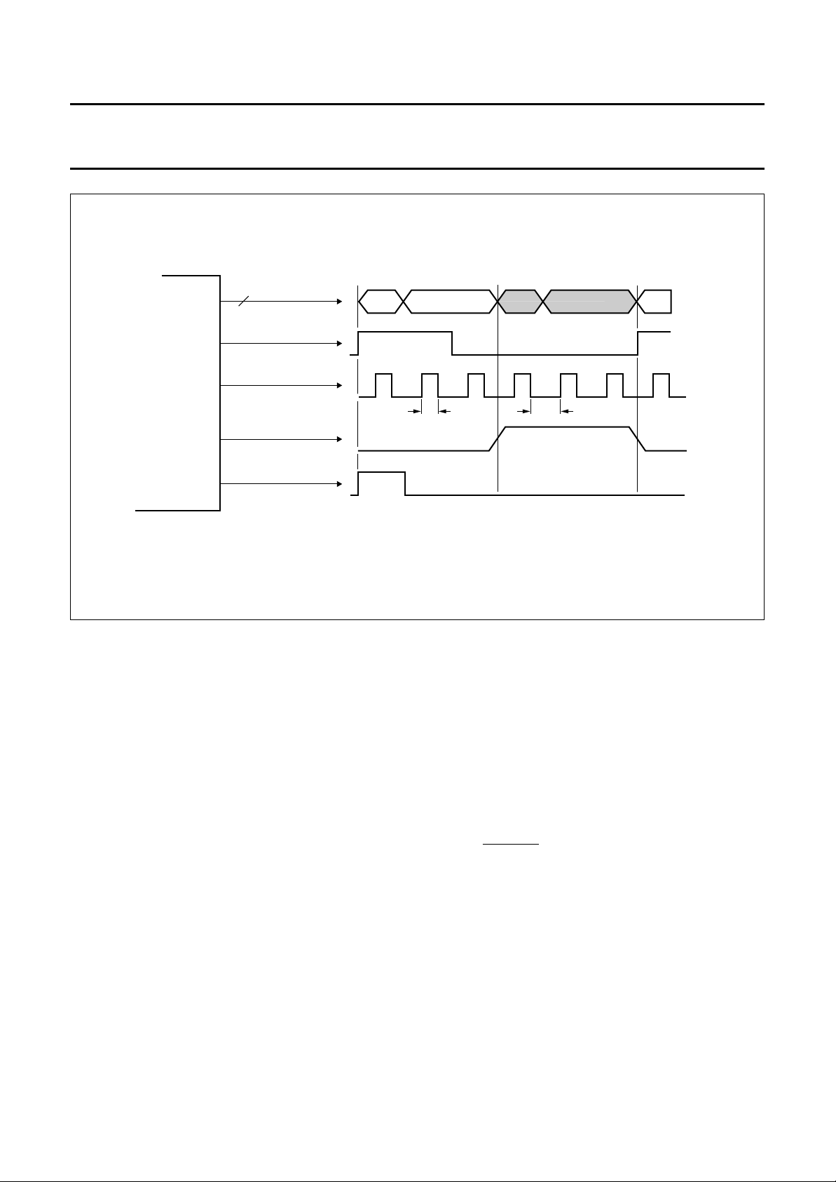
7.6 Interfacing to Philips SAA7201 video decoder
The Generic Data Filter (GDF) is connected to the General
Purpose interface, which shares its output bus
GPO7 to GPO0 with the high speed data interface.
This output can be used to interface with the Philips
SAA7201 video decoder. The GDF does not filter at all, it
merely passes the entire transport stream to the output in
byte format. The filter generates a GPST signal, which is a
gated byte clock, defined by a fixed high time (t
a minimum low time (t
) (see Fig.9). In addition to the
CLKOL
CLKOH
) and
strobe signal, the filter generates a GPV signal which can
be used in combination with the continuous DCLK to select
valid bytes, should a continuous clock be needed.
The filter furthermore generates a packet sync byte
indicator (GPSYNC).
1 byte 1 byte
t
t
CLKOH
CLKOL
MGG769
The general purpose interface is bidirectional and can
therefore serve as an alternative transport stream input to
the demultiplexer. The mode of the general purpose
interface is set by configuring the ‘GP_direction’ bit
(input = 1, output = 0, address 0x0700, see Table 13).
The GP pins have the following meaning when configured
to operate as inputs:
GPO7 to GPO0 = PKTDAT7 to PKTDAT0
GPST = PKTBCLK
GPSYNC = PKTSYNC
GPV = PKTDATV
HSE =
PKTBAD.
It should be noted that the HS filter is programmed to
section mode (see Table 4), the general purpose output is
not available.
1997 Jan 21 19
Page 20

Philips Semiconductors Preliminary specification
MPEG-2 systems demultiplexer SAA7205H
handbook, full pagewidth
GPO7 to GPO0 byte 187 sync byte (0)
GPST
GPSYNC
GPV
consecutive transport packet bytes
t
CLKOH
Fig.9 Signal constellation for general purpose interface (SAA7201 compatible).
7.7 Interfacing to a third party video decoder
Communication to a third party video decoder involves
merging both video packetized elementary stream (PES)
or elementary stream (ES) data and control data on the
same 8-bit bidirectional bus VO7 to VO0 (see Fig.10).
PES or ES (bit: ‘video_pes_esn’, address 0x050A, see
Table 13) data is filtered by the video data filter and is
passed to a 768 Byte video FIFO buffer (see Section
“Output buffering for audio and video”), in which it is stored
at byte clock frequency (9 MHz). The video PES or ES
stream is read from the FIFO at video data acquisition
clock frequency
CLKP (equals 9 MHz = CCLKI/3, 67%
duty cycle, see Fig.10). However, CLKP is a gated clock
signal, which is frozen to logic 1 in case of control
exchange between the microcontroller and the video
decoder (⇒ VSEL = 0), or FIFO underflow (see Fig.10).
A bidirectional bus multiplexer (‘Merger’) is therefore
located at the output of the video FIFO. The timing
associated with the video output interface is illustrated in
Fig.11.
t
CLKOL
byte 1
bytes 2 to 187
The third party video interface outputs clock and
synchronization references. The set of references consists
of a 13.5 MHz clock (CLK13.5, programmable phase, bit:
‘clk_13p5_pol’, address 0x050A, see Table 13), a CbREF
signal,
“CCIR 601”
compliant H, V, composite syncs, and
a field parity (EVEN/ODD) signal (both 50 Hz and 60 Hz,
bit: ‘ccir_50_60n’, address 0x050A, see Table 13).
The CbREF signal is locked to CCLKI and indicates
U samples in the UY/VY video decoder output.
To compensate for the delay in the decoding path, the
phase of CbREF (active LOW) is programmable as
illustrated in Fig.13 [bits: cb_ref_phase (1 to 0)], address
0x050A, see Table 13). The clock period immediately
following a COMSYNC falling edge in normal lines (equals
HSYNC falling edge) corresponds to counter position 0,
the clock period preceding the falling edge corresponds to
position 1727 (50 Hz), or 1715 (60 Hz),
MGG770
1997 Jan 21 20
Page 21
Philips Semiconductors Preliminary specification
MPEG-2 systems demultiplexer SAA7205H
The set of references can be generated either in master
(internal), or in slave (external) mode. Both options are
compared in Fig.12. If bit ‘v_in_pol’ (address 0x050A,
see Table 13) is programmed to logic 1, the sync
generator synchronizes to a rising edge on VIN, or it locks
to a falling edge. The sync circuitry automatically operates
in slave mode, if an appropriate edge occurs on VIN.
The position in the
CCIR 601
field at a VIN triggering edge
is determined by the programmable registers ‘horiz_offset’
and ‘verti_offset’ (addresses 0x050F and 0x0510,
see Table 13). The phase relationships between the
COMSYNC and the HSYNC and VSYNV are
programmable (words: ‘h_sync_fall’, ‘h_sync_rise’,
‘v_sync_fall’, ‘v_sync_rise’, addresses 0x050B to 0x050E,
see Table 13). For details on the sync signal constellation
see Fig.13. It should be noted that the sync generator is
not reset by ‘Pwr_On_Rst’.
In the slave mode, the demultiplexer offers a possibility to
lock the 27 MHz system clock to the incoming vertical sync
pulses (VIN). The demultiplexer stores the position of the
horizontal and vertical sync counters as soon as a
triggering edge occurs on VIN (‘vin_hpos’, ‘vin_vpos’,
addresses 0x0408 and 0x0409, see Table 13).
The triggering edge furthermore resets the H and V
counters. The microcontroller can retrieve the position
data and calculate the difference between the detected
position and the required position (horiz_offset,
verti_offset). From this the microcontroller is able to derive
VCO control values (see Section “Program clock reference
processing”). The 27 MHz system clock can thus be
locked to external display sync sources.
handbook, full pagewidth
TS
CSDEM VSEL
VSEL = 1
VO7 to VO0
DMUX
MUX
FIFO
control
MICROCONTROLLER
CLKP
MDAT7
to
MDAT0
t
CLKOL
VO7 to VO0
video/control
CLKP
address
CSVID
VIDEO
(THIRD
PARTY)
t
CLKOH
video FIFO
output
1
VSEL
MGG772
DATA
1
VSEL
VO
MUX
Fig.10 Merger of video elementary stream and video control data within the demultiplexer.
1997 Jan 21 21
Page 22

Philips Semiconductors Preliminary specification
MPEG-2 systems demultiplexer SAA7205H
Table 5 VSEL = 0; see Fig.10
R/W CSVID = 0 CSVID = 1
W = 0 DMUX drives VO7 to VO0
R/
DMUX does not drive MDAT7 to MDAT0
W = 1 DMUX does not drive VO7 to VO0
R/
DMUX drives MDAT7 to MDAT0 DMUX does not drive MDAT7 to MDAT0
handbook, full pagewidth
VSEL
R/W
Address
CSVID
MDAT7
to MDAT0
VO7 to VO0
t
1
t1=2×111 = 222 ns.
t2= demultiplexer throughput delay = 24 ns.
t3>0ns
t4> 5 ns.
t5< 17 ns.
≤90 µs ≥360 µs
to video from video
to video from video video datavideo data
t
2
t
3
t
4
t
2
t
5
t
1
MGG773
Fig.11 Video output interface timing diagram (read and write cycle).
1997 Jan 21 22
Page 23
Philips Semiconductors Preliminary specification
MPEG-2 systems demultiplexer SAA7205H
handbook, halfpage
Internal timing
reference
÷
CCLKI
DMUX
CLK13.5
CbREF
HSYNC
COMSYNC
VSYNC
EVEN/ODD
PWMO
External timing
reference
CCLKI
VIN
DMUX
÷
Fig.12 Reference timing alternatives.
CLK13.5
CbREF
HSYNC
COMSYNC
VSYNC
EVEN/ODD
PWMO
MGG774
1997 Jan 21 23
Page 24
Philips Semiconductors Preliminary specification
MPEG-2 systems demultiplexer SAA7205H
dbook, full pagewidth
626 half lines
VSYNC rise
VSYNC fall
MGG775
. . . .1726 1727 0 1 2 3 4 5 6 7 . . . . .
623 624 0 1 2 3 4
624 half lines
COMSYNC
EVEN/ODD
VSYNC
(= field_sync!)
(half line count)
COMSYNC
1997 Jan 21 24
HSYNC fall HSYNC rise
0 1 2 3 4 5 6 7 . . . .
HSYNC
(pixel count)
CCLKI
2468101214161820222410 35791113151719212325
CLK 13.5
CbREF
('clk_13p5_pol' = '0')
Fig.13 Reference timing (CCIR 601; 50 Hz).
"01" "10" "11" "00"
cb_ref_phase
Page 25

Philips Semiconductors Preliminary specification
MPEG-2 systems demultiplexer SAA7205H
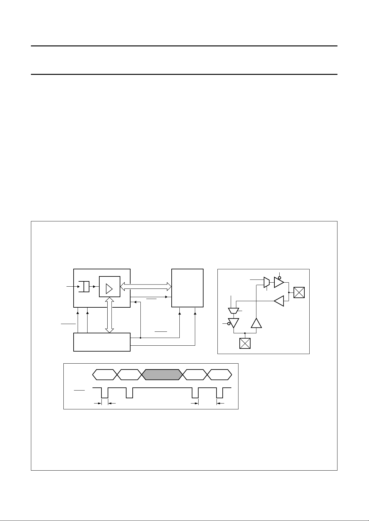
7.8 Interfacing to SAA2500 and third party audio decoders
The audio interface performs system support for Philips
SAA2500 or third party audio decoders. The pin
assignment for the interface and a description of the
respective functions is given in Table 6. Audio PES or
elementary stream data are filtered by the audio data filter
and passed to a 6 kByte FIFO buffer in which they are
stored at the byte clock frequency (9 MHz). Audio
elementary stream data is read from the FIFO at the
AUDATCLK frequency. The frequency of this clock is
adapted to the audio bit rate index (32 to 448 kbit/s), which
is derived from audio frame header information. However,
to compensate for decoder delays, the output process is
conditioned to synchronize to presentation time stamps
(PTS).
The AUDECLK output is derived from the 27 MHz
demultiplexer chip clock through division by a real
number M, which is generated by programming I0 and I1
(words: ‘audio_incr0’, ‘audio_incr1’, addresses 0x060B
and 0x060C, see Table 13). The AUDECLK can be used
as an audio decoder chip clock and is generated by the
circuitry illustrated in Fig.14. The decoder clock is
generated with a maximum edge jitter of 37/2 = 18.5 ns.
Therefore, if this clock is used for audio digital-to-analog
conversion, for high quality audio it may have to be
dejittered using an external PLL or an LC filter.
Since most audio decoders accept only elementary audio
data, the demultiplexer takes care of the following basic
tasks in the audio path:
• Parsing of audio transport packets with the proper PID
• Suppression of transport packet header data
• Detection of PES packet boundaries to find PES packet
length and PTS time stamps
• Suppression of PES headers and stuffing bytes (bit
‘audio_pes’, address 0x060A, see Table 13), optional
• Detection of audio frame boundaries to find audio frame
length and audio bit rate, optional
• Delay compensation and expansion of audio data to the
correct time and bit rate (bit ‘uc_sw_sync’, address
0x060A, see Table 13), optional.
A block diagram of the audio interface circuitry is illustrated
in Fig.15.
One basic function of the audio data filter is to optionally
determine the audio frame length and find the frame
boundaries. The audio frame length depends on the basic
audio sampling frequency, the coded bit rate, the MPEG
layer used and in case of 44.1 kHz sampling frequency,
the padding bit. The frame length ranges between
32 and 1728 bytes. All frame length related data are
coded in the audio frame header directly after the sync
word. Since the 12-bit sync word is not unique and could
be emulated in the audio stream, a recursive detection
algorithm consisting of the following steps is implemented:
1. Detect first occurrence of sync word
2. Evaluate header and determine frame length
3. If frame length is non valid go to step 1
4. Check whether a sync word exists at frame length
distance in the stream
5. If no valid sync word is detected at this position go to
step 1
6. If sync word is valid go to step 2.
All relevant header parameters are stored in dedicated
registers. Their value is used for internal control but can
also be accessed by the external microcontroller (words:
‘audio_frame_length’, ‘audio_frame_info’, addresses
0x0611 and 0x0612, see Table 13).
The delay of the audio data from input to output of the
FIFO is basically determined by PTS time stamps. In order
to avoid difficult PTS management these time stamps are
stored in the FIFO between consecutive audio frames
(see Fig.15). If a PTS exists for one specific audio frame
the 23 least significant bits of the 33-bit time stamp are
stored together with a PTS_valid flag in three byte
positions preceding the associated audio frame. If no PTS
is available, three bytes are also inserted preceding the
audio frame, but in this case the PTS_valid flag indicates
that the remaining 23 bits may not be interpreted as a valid
PTS (see Fig.15).
The input process to the audio FIFO operates in stand
alone, but can be restarted by the microcontroller
(bit ‘µc_frc_restart’, address 0x060A, see Table 13).
During restart, the write address counter is reset to 0 and
kept at this position until the first audio frame with a valid
PTS is available from the stream. The storage of PTS plus
elementary audio data is then started. The storage
process continues as long as the detected audio frame
length remains the same. If a change in frame length
occurs, or if a sync word is missing, the write counter is
reset to 0 automatically and data storage is halted until a
valid audio frame with associated PTS is retrieved from the
stream. This kind of discontinuity handling is performed
unconditionally and is signalled to the external
microcontroller (interrupt: ‘irpt_audio_restart’, address
0x0000, see Table 13).
1997 Jan 21 25
Page 26

Philips Semiconductors Preliminary specification
MPEG-2 systems demultiplexer SAA7205H
The FIFO output process can operate in stand alone, but
it can also be controlled by the microcontroller. During
start-up the read address counter is reset to 0. After the
FIFO input process is started the first PTS is retrieved from
the first three byte positions in the FIFO. To this PTS value
a programmable offset is applied [resulting in: PTS* = PTS
- ‘audio_pts_offset’, addresses 0x060D to 0x060E (two’s
complement), see Table 13] to compensate for the delay
of the audio decoder. The FIFO output process is
subsequently put on hold as long as the System Time
Clock (STC) counter has not reached the value of PTS*.
When the STC counter exceeds the PTS* position the
output process is started and audio data is retrieved from
the FIFO at a speed indicated by the bit rate parameter in
the frame header (32 to 448 kbit/s).Only valid audio data is
passed to the output. Each time a valid PTS occurs at the
FIFO output the difference between PTS* and STC is
calculated and stored, to enable reading by the
microcontroller (words: ‘audio_stc_min_epts’, addresses
0x060F to 0x0611, see Table 13). Two modes of
operation can be selected by the microcontroller (bit
‘µc_free_run’, address 0x060A, see Table 13):
• PTS controlled: (‘µc_free_run’ = 0) the output process is
put on hold if PTS* is greater than the STC counter
position. Otherwise the output process continues at the
given bit-rate. In this mode, the output process could be
halted for every valid PTS which is being output by the
FIFO.
• Free running: (uc_free_run = 1) the output process is
synchronized once during start-up only and continues at
the derived bit rate without resynchronizing to new PTS
time stamps. The difference between PTS* and the STC
value is sampled and stored at the moment a PTS is
taken from the FIFO (words: ‘audio_stc_min_epts’,
addresses 0x060F to 0x0611, see Table 13). This event
is signalled to the microcontroller (interrupt:
‘irpt_audio_diff’, address 0x0000, see Table 13).
A decision for a restart (bit ‘µc_frc_restart’, address
0x060A, see Table 13) can consequently be taken in
software, whenever the difference ‘audio_stc_min_epts’
exceeds a certain audible threshold (20 ms for
instance).
After the input process is started a continuous check is
performed on the distance between the FIFO read and
write counters. If one pointer approaches the other one a
wrap around may take place (buffer underflow or
overflow), causing synchronization to be lost completely.
Should this occur an internal start-up (restart) is initiated
automatically and signalled to the microcontroller
(interrupt: ‘irpt_audio_restart’, address 0x0000,
see Table 13).
If a third party audio decoder is capable of adjusting the
output delay by itself, the demultiplexer audio output
process does not have to be PTS controlled. In this case
the functionality of the demultiplexer audio interface can
optionally be reduced to (bit ‘µc_sw_sync’ = 1, address
0x060A, see Table 13):
• Parsing of audio transport packets with the proper PID
• Suppression of transport packet header data
• Detection of PES packet borders to find PES packet
length and PTS time stamps
• Suppression of PES headers and stuffing bytes (bit
‘audio_pes’, address 0x060A, see Table 13), optional
• Time expansion of the audio transport packet payload.
In this so called software sync mode (‘µc_sw_sync’ = 1)
the FIFO input runs freely. Either entire PES packets (bit
‘audio_pes’ = 1, address 0x060A, see Table 13), or the
payload of selected PES packets is stored in the FIFO at
subsequent addresses starting from 0 at start-up.
PTS information is stored in the FIFO but is also available
in registers to make it accessible for the microcontroller
(words: ‘audio_pts’, addresses 0x0601 to 0x0602,
see Table 13).
In the software sync mode, the FIFO output process is
controlled by the microcontroller. The read address
counter is reset to 0 during start-up and stays at this
position until the write address exceeds the read address.
This is the case immediately after the input process starts.
The output process subsequently starts reading data at a
fixed data rate of 9 Mbit/s (AUDATCLK = 9 MHz, 67% duty
cycle (see Table 6 and Fig.10). The output process
continues outputting data as long as the read address
does not exceed the write address. If the read address
equals the write address the output stops (AUDATV is set
to logic 0) until new data is received at the input and the
write address counter increments again. Consequently, if
audio transport packets are equally distributed along the
transport stream, the FIFO remains almost empty.
The FIFO cannot overflow if the output rate equals at least
the average input rate. Given a capacity of 6 kByte for the
FIFO this means that at least 30 audio transport packets
can be stored before an overflow occurs.
Audio data can be downloaded by the microcontroller to
enable generation of ‘beeps’. For this purpose, the
demultiplexer has to be set to download mode (bit
‘µc_downl’ = 1, address 0x060A, see Table 13).
1997 Jan 21 26
Page 27

Philips Semiconductors Preliminary specification
MPEG-2 systems demultiplexer SAA7205H
The microcontroller must first force the audio interface to restart (µc_frc_restart = 1). Subsequently it may download
compressed audio data by writing consecutive bytes to the audio buffer (address 0x1xxx, see Table 13). A ‘beep’ must
always consist of valid packetized elementary stream (PES) data. If the ‘beep’ is to be output to the audio decoder in
PES format, ‘audio_pes’ must be set to logic 1. If the audio interface is programmed to software sync mode, the PES
headers do not have to contain PTS data words. However, if the ‘beep’ has to occur at a specific point in time, the
hardware sync mode (µc_sw_sync = 0 and µc_free_run = 1) is most suitable and at least the first PES header has to
contain a valid PTS.
Table 6 SAA2500 and third party audio output interface
PIN I/O MODE FUNCTION
AUDAT O normal, SAA2500 and
gated clock
ADATCLK O both normal and SAA2500 continuous audio data acquisition clock, 32 to 448 kHz, or
gated clock gated audio data acquisition mode, 32 to 448 kHz.
AUDECLK O normal, SAA2500 and
gated clock
AUDATV O normal mode, gated clock valid audio data indicator (microcontroller SAA2500 = 0)
SAA2500 mode audio sync word indicator (microcontroller SAA2500 = 1)
AUE O normal mode, gated clock audio data error flag (active LOW)
SAA2500 mode sampling frequency indicator; logic 1 for 44.1 kHz, logic 0 for
audio elementary stream data, clocked out 111 ns after an
AUDATCLK rising edge in 32 to 448 kHz mode, and 74 ns
after an AUDATCLK rising edge in 9 MHz mode
9 MHz
AUDATCLK = 0 in case of invalid data (gated_clock = 1,
address 0x060A, see Table 13)
continuous audio decoder chip clock (N × 27 MHz/M)
the other frequencies
handbook, full pagewidth
CCLKI
27 MHz
27
27
f
1
divide-by-M
0
I
0
1
I
1
f
o
11.29
12.288
C
o
+
M
12
12 (b 0 to 11)
12
2.392 (= 3750/1568)
2.197 (= 3375/1536)
DFF
Fig.14 Audio descrambler clock circuit and programming examples.
1997 Jan 21 27
I
1568
1536
fo = 256f
= 11.29 or 12.288 MHz
12
0
1914 (= 1568 + 4096 − 3750)
2257 (= 1536 + 4096 − 3375)
= AUDECLK
s
I
1
MGG776
Page 28

Philips Semiconductors Preliminary specification
MPEG-2 systems demultiplexer SAA7205H
ndbook, full pagewidth
SYNC WORD
MICRO-
SAMPLE FROM
INTERFACE
CONTROLLER
AUDIO DATA
LAYER
BIT RATE
FILTER
PADDING
AUDAT
EXTRACT
INSERT
AUDIO
FRAME
AUDATV
AUE
PTS
FIFO
PTS
3 BYTES
DATA
PARSING
APPLY
OFFSET
WRITE
ADDRESS
COUNTER
FRAME
LENGTH
CALCULATE
READ
ADDRESS
COUNTER
OUTPUT
GENERATE
RATE
(1)
PTS
FIFO
CONTROL
ADATCLK
AUDECLK
MGG777
PTS_valid indicator bit: '1' if PTS is valid, '0' otherwise
PTS
PTS
STUFFING
PES
DATA
PARSING
PROCESSING
PARSER
TRANSPORT
DATA
PARSING
PCR
VCO
CONTROL
1997 Jan 21 28
STC
PCR
PROCESSOR
DIVIDER
audio frame data audio frame data23 bits PTS
23 bits PTS
FIFO format of audio data in ES mode (audio_pes = 0):
Fig.15 Audio data filtering and delay compensation.
Page 29

Philips Semiconductors Preliminary specification
MPEG-2 systems demultiplexer SAA7205H
7.9 Interfacing to combined audio/video decoders
If the audio and video interfaces are programmed to the
A/V combined mode (av_combi = 1, address 0x060A,
see Table 13) they assume operation as illustrated in
Fig.16. The microcontroller controls the VO bus in much
the same way as described in Section “Interfacing to a
third party video decoder”. If VSEL = 0, the demultiplexer
sets up a transparent path between the microcontroller
and the combined A/V decoder (see Section “Interfacing to
a third party video decoder”). However, If the data level in
the video FIFO reaches a programmable overflow
threshold (‘v_ovfl’, address 0x0512, see Table 13), a
non-maskable interrupt (
indicates that the microcontroller must release the VO bus,
otherwise video data is lost. As soon as the data level in
the video FIFO reaches the programmable underflow
threshold (‘v_undfl’, address 0x0512, see Table 13), NMI
is driven HIGH again.
NMI) is pulled LOW. This
Audio and video data are output at the request of the
combined A/V decoder, as illustrated in Fig.16 (
AUDATR). If an A/V decoder does not have such a
request, these demultiplexer inputs may be grounded.
In the A/V combined mode, both CLKP and AUDATV can
be used as data valid signals (see Fig.16). Timing figures
for these valid signals are as indicated for CLKP in Fig.10.
Audio and video data are output in a sequence of, for
instance, four video bytes followed by one audio byte.
The length of this sequence is programmable and is
repeated incessantly. However, if the audio FIFO is empty,
or AUDATR is HIGH, a video byte is output, even in audio
time slots (see Fig.16), if VREQ is LOW. Audio data
however, are never output in video time slots.
VREQ,
1997 Jan 21 29
Page 30

Philips Semiconductors Preliminary specification
MPEG-2 systems demultiplexer SAA7205H
handbook, full pagewidth
VSEL
NMI
VREQ
AUDATR
VO
VREQ
AUDATR
overflow
threshold
VIDEO FIFO
video only A and V A and V
underflow
threshold
audio only
NMI
micro-
controller
bus
video FIFO level
at overflow
threshold
video
underflow
video FIFO level
at underflow
threshold
video only
audio
underflow
CLKP
AUDATV
VO
VVVVVVVVVAVVVVAV
1234512345123451234 12345
Fig.16 Interfacing to combined audio/video decoders.
1997 Jan 21 30
VV V
MGG778
Page 31

Philips Semiconductors Preliminary specification
MPEG-2 systems demultiplexer SAA7205H
7.10 Interfacing to SAA9042 and SAA5270 teletext decoders and SAA7183 EURO-DENC
The Demultiplexer contains a ITU-R System B compatible
Teletext (TXT) filter. This filter extracts relevant data from
the incoming data stream in accordance with the syntax
specified by the European Telecommunications Standards
Institute (ETSI). The TXT filter interprets the data, provides
temporary storage (2 kBytes) and outputs the data in a
TTC/TTD protocol (compatible with SAA9042 and
SAA5270), or in a TTR/TTX protocol (compatible with
SAA7183). The TTC/TTD output protocol is shown in
Fig.17 and the connection of SAA9042 to the
demultiplexer is shown in Fig.18. The SAA9042 and
SAA5270 teletext decoders are assumed to operate in
‘Normal Synchronous Mode’, applying 4 channel
acquisition. Some of the options associated with MPEG2
PES packets, such as PTS handling and CRC checking
are not implemented in the demultiplexer TXT filter.
The TXT filter does support interfacing with the
microcontroller, for use with future extensions such as
Close Caption (CC) and OSD. The TXT filter can therefore
be used to retrieve full PES packets. Various modes of
operation can be configured (address 0x0800,
see Table 13).
The PID of the TXT filter is programmable ‘txt_pid’
(address 0x0801, see Table 13). The delay between an
active horizontal sync edge and the start of TTD/TTX
output is controlled by sync_to_window_delay ‘sw_del
[6 to 0]’ (address 0x0802, see Table 13). The active
horizontal sync edge is defined by ‘sync_parity’ (address
0x0800, see Table 13), logic 0 meaning falling edge. All of
the control registers are write only. The TXT filter however
also has some readable registers which contain the
current values of PES scrambling control, PES flags
(address 0x0805, see Table 13), data_identifier,
data_unit_identifier (address 0x0806, see Table 13,) and
data_unit_flags (address 0x0807, see Table 13,).
The status register of the TXT filter (address 0x0808,
see Table 13) contains the current error code and the
number of 16-bit words in the TXT FIFO.
The TXT interface is capable of supporting TXT insertion
into the vertical blanking interval of a CVBS signal. For this
purpose, it provides an SAA7183 (EURO-DENC)
compatible TXT output. If EURO-DENC requests data via
TTR, the demultiplexer provides it at 6.9375 Mbit/s. This
frequency is generated by dividing 27 MHz by 3 or 4 in a
specific sequence. The rhythm required by the
EURO-DENC is exactly matched. The interpretation of the
field_parity bit, in the TXT data stream, is programmable
(‘parity_sign’, address 0x0800, see Table 13). Allocation
of TXT data to odd or even fields can therefore be
configured as desired. Field allocation can be switched on
or off with ‘check_field’ (address 0x0800, see Table 13).
The TXT filter can be separately enabled by setting the
input and output modes to ‘idle’ (see Table 7) in the
txt_mode register (address 0x0800, see Table 13) and
reset (‘txt_reset’, address 0x0804, see Table 13). When
the TXT filter is used in one of the microcontroller
interaction modes close_caption or µc_download, the
FIFO may generate a warning that the TXT_FIFO is almost
full. The threshold for this warning can be set to any value
between 0 and 1023, being the number of 16-bit words in
the TXT_FIFO (‘fifo_tresh [9 to 0]’, address 0x0803,
see Table 13). An interrupt is also generated at the
moment an overflow occurs. At this point the TXT_FIFO is
automatically reset to empty. If the microcontroller is
writing to the TXT_FIFO, overflow must be prevented and
the reset must be performed by the microcontroller.
Table 7 TXT filter modes and error codes
CODE TXT INPUT MODE TXT OUTPUT MODE TXT_FIFO ERROR CODE
00 idle idle no error
01 teletext TTC/TTD threshold passed
10 close_caption TTXrq/TTX overflow
11 µc_download idle not used
1997 Jan 21 31
Page 32

Philips Semiconductors Preliminary specification
MPEG-2 systems demultiplexer SAA7205H
handbook, full pagewidth
TXT FIFO data format:
HSYNC
TTC
TTD
12 µs
'sync_parity' set to 0, 'sw_del [8 to 0]' set to 0 × 51.
TTC
TTD
reserved
21 5 8 16
field_parity line_offset
6.75 MHz continuous clock
(6.75 MHz)
framing_code
43 bytes
64 µs
magazine
and packet
address
TXT data bytes
40 × 8 = 320 bits
Fig.17 Teletext output protocol for teletext decoders.
1997 Jan 21 32
output to TXT decoder
MGG779
Page 33

Philips Semiconductors Preliminary specification
MPEG-2 systems demultiplexer SAA7205H
handbook, full pagewidth
CLK13.5
DMUX
HSYNC
VSYNC
13.5 MHz
TTC
TTD
TTR
Fig.18 Demultiplexer - Teletext decoder interconnection.
7.11 Program clock reference processing
To provide a reference for all timing related actions, two
System Time Counters (STC) are implemented in the
demultiplexer. Each system time counter is split up into
two counters as illustrated in Fig.20. This split has the
advantage that the STC output has the same format as the
incoming PCRs, thus enabling direct comparison.
The STC counters (both of them 9 + 24 bits) are compared
with PCRs alternately. In a selected stream (word:
‘pcr_pid’, address 0x0401, see Table 13), PCR values are
transmitted at least once every 100 ms in the adaptation
field of a transport header. Each STC counter is therefore
updated once every 200 ms. Whenever a new PCR value
is retrieved (‘irpt_discnt_a’, or ‘irpt_discnt_b’, address
0x0000, see Table 13), both its value and the value of the
difference ∆PCR = PCR - STC can be read by the
microcontroller (words: ‘pcr_base_msw’, ‘pcr_base_lsw’,
‘pcr_ext’, ‘pcr_base_diff_msw’, ‘pcr_base_diff_lsw’,
‘pcr_ext_diff’, addresses 0x0402 to 0x0407,
see Table 13). The STC counters are preset in turn to the
PCR timing reference, as illustrated in Fig.19. If an STC
counter is preset, the other is used as a timing reference
for PTS/DTS comparison. It should be noted that preset
operations may cause discontinuities and may render
PTS/DTS time stamps obsolete.
LL3A LL3D
TTC
TTD
HSA
HSA
SAA9042
(Reg 17, bit 6 = 0
for normal
acquisition mode)
VSD VSA
display
sync
MGG780
threshold, the microcontroller can postpone the switching
from the continuous STC counter to the one that was
preset, as indicated by the vertical dotted line in Fig.19.
For this purpose the microcontroller drives the signal
‘stop_toggle’ to logic 1 (address 0x0400, see Table 13) as
soon as it detects ∆PCR > threshold. If ‘stop_toggle’ is
reset, toggling between the STC counters continues,
starting with taking as a reference the STC that is most up
to date.
The measured phase offset (∆PCR_ext, ∆PCR_base) is
filtered by the microcontroller to derive control data for an
externally implemented crystal oscillator. To avoid having
to implement DACs in the demultiplexer, a duty cycle
controlled Pulse Width Modulated (PWM) output is
implemented. The PWM circuit connected to this output
delivers a pulse width modulated signal, the ratio of HIGH
and LOW time which is adjustable by the microcontroller
(byte: ‘pwm_ctrl [7 to 0]’, address 0x0511, see Table 13).
A ‘pwm_ctrl’ value of 127 corresponds to a ‘Pwm_Out’
signal with a 50% duty cycle, higher values represent a
higher duty cycle. The pulse width modulated signal can
be filtered externally by an RC filter to create a control
signal for a crystal oscillator. The PLL loop bandwidth for
the clock regeneration circuit is determined in software.
An application diagram is shown in Fig.21.
Two STC counters are implemented to cope with decoding
problems resulting from discontinuities. Discontinuity
handling is left to the microcontroller. After a discontinuity,
if ∆PCR (equals PCR - STC) exceeds a certain (software)
1997 Jan 21 33
The 27 MHz system clock can be locked to an external
display sync source (see Section “Interfacing to a third
party video decoder”).
Page 34

Philips Semiconductors Preliminary specification
MPEG-2 systems demultiplexer SAA7205H
handbook, full pagewidth
STC-A
incoming
PCR
STC-B
'stop_toggle'
∆PCR-a ∆PCR-a ∆PCR-a ∆PCR-a
reference
for PTS
reference
for PTS
∆PCR-b ∆PCR-b∆PCR-b∆PCR-b
> threshold
reference
for PTS
reference
for PTS
reference
for PTS
MGG781
Fig.19 Example of PTS/DTS reference switching.
1997 Jan 21 34
Page 35

Philips Semiconductors Preliminary specification
MPEG-2 systems demultiplexer SAA7205H
handbook, full pagewidth
CCLKI
(27 MHz)
transport
stream
DIVIDE-BY-3
load A or B
when new PCR
arrives
9 MHz
PCR EXTENSION
9 bits
−
9
COU NTER
COUNTER
0 to 299 (step 3)
back-end part runs
on byte clock (9 MHz)
PCR REGISTERS
load A or B
when new PCR
arrives
90 kHz
COUNTER
STC COUNTER-B
PCR BASE
24 LSBs
−
24
COUNTER
24
0 to 2
microcontroller
interface
PCR received
of 33
∆PCR_ext
∆PCR_base
STC_samples
− 1
PTS REGISTERS
PTS REGISTERS
PTS-BASE
Fig.20 PCR and PTS/DTS processing implementation.
1997 Jan 21 35
−
−
emulated_PTS
incoming_PTS
interrupt upon
zero transition
MGG782
Page 36

Philips Semiconductors Preliminary specification
MPEG-2 systems demultiplexer SAA7205H
handbook, full pagewidth
MICROCONTROLLER
(LOOP FILTER)
DMUX
CCLKI (27 MHz)
Fig.21 VCO control for local time reference regeneration.
7.12 Time stamp processing (PTS/DTS)
Time stamp processing generates decoding (DTS) or
presentation (PTS) start interrupts for source decoders
(bits: ‘irpt_audio_strt’, irpt_video_strt’, address 0x0000,
see Table 13). Each time the stamp processor therefore
compares emulated PTS/DTS values (word:
‘video_emu_pts’, addresses 0x0505 and 0x0506, or
‘audio_emu_pts’, addresses 0x0605 and 0x0606,
see Table 13) to the local system time clock (STC,
see Fig.20). An interrupt (IRQ) to the microcontroller is
generated in the event of a positive zero transition of the
differences (STC - ‘video_emu_pts’ and STC ‘audio_emu_pts’).
Interrupt-handling routines in the microcontroller translate
the demultiplexer interrupt to control and synchronization
data for the attached source decoder, as illustrated in
Fig.23 for the video time stamp processor. Figure 23
assumes that PTS/DTS are retrieved inside the video
decoder, but this is not necessary. The demultiplexer also
retrieves PTS/DTS words from the stream (words:
‘video_pts’, ‘video_dts’, addresses 0x0501 to 0x0504,
see Table 13). In contrast to what is illustrated in Fig.23,
video PTS/DTS processing could therefore be identical to
audio PTS/DTS processing (see Fig.24).
While the third party video decoder could retrieve
PTS/DTS data from the incoming PES stream, the audio
decoder generally does not. PTS/DTS retrieval is therefore
performed in each of the time stamp processors
control voltage
PWMOVOR
C
OSCILLATOR
MGG783
(audio and video) within the demultiplexer. It is for the
microcontroller to decide whether it uses the retrieved time
stamps. For audio time stamp processing the
microcontroller may want to use the values retrieved by the
demultiplexer (words: ‘audio_pts’, audio_dts’, addresses
0x0601 to 0x0604, see Table 13) when operating in the
software controlled synchronization mode. In this mode
(bit ‘µc_sw_sync’ = 1, address 0x060A, see Table 13) the
microcontroller loads emulated PTS values into the
demultiplexer (words: ‘audio_emupts’, addresses 0x0605
to 0x0606, see Table 13) to get it to generate start
interrupts (interrupt: ‘irpt_audio_strt’, address 0x0000,
see Table 13), as illustrated in Fig.23. However, audio
synchronization can also be performed automatically by
the demultiplexer (bit ‘µc_sw_sync’ = 0, address 0x060A,
see Table 13) (see Section “Interfacing to SAA2500 and
third party audio decoders”).
The microcontroller has to perform time stamp emulation
on the basis of incoming PTS/DTS values (words:
‘audio_pts’, ‘audio_dts’, addresses 0x0601 to 0x0604,
see Table 13). Emulation involves compensation for
source decoder internal delays and repetitive generation
of time stamps. The latter could be necessary because
time stamps could be needed for every access unit in an
elementary stream, but are broadcast far less frequently.
It should be noted that video PTS/DTS processing can
operate along the same lines as illustrated in Fig.23 for
audio decoders.
1997 Jan 21 36
Page 37

Philips Semiconductors Preliminary specification
MPEG-2 systems demultiplexer SAA7205H
handbook, full pagewidth
PES
STC
STC>PTS*
PTS/DTS
PTS*/DTS*
DMUX VIDEO
handbook, full pagewidth
IRQ
IR HANDLING
EMULATION
MICROCONTROLLER
control/sync
MGG784
Fig.22 Example of PTS/DTS processing for a third party video decoder.
ES
STC
STC>PTS*
PTS/DTS
PTS*/DTS*PTS/DTS
DMUX AUDIO
Fig.23 Example of PTS/DTS processing for a third party audio decoder.
1997 Jan 21 37
IRQ
IR HANDLING
EMULATION
MICROCONTROLLER
control/sync
MGG785
Page 38

Philips Semiconductors Preliminary specification
MPEG-2 systems demultiplexer SAA7205H
7.13 Output buffering for audio and video
Output buffering for both audio and video is based on
FIFOs and buffer control circuitry. For audio, a 6 kByte
buffer is needed in which data is written at byte clock
frequency (9 MHz). Data is output bit serially via pin
AUDAT, at AUDATCLK frequency, which is adjusted to the
bit rate of the audio data (32 to 448 kbit/s, or 9 Mbit/s
(software sync mode)). Alternatively, in audio/video
combined mode, audio data is output byte parallel at rates
determined by ‘av_ratio’ (see Section “Interfacing to
SAA9042 and SAA5270 teletext decoders and SAA7183
EURO-DENC”). Valid audio elementary stream data is
indicated by AUDATV = 1. In case of buffer underflow,
AUDATV is kept LOW, unless the combined audio/video
mode is configured (see Fig.16). The audio FIFO is used
to overcome clock interfacing problems and to provide
sufficient delay to synchronize audio and video. The buffer
output process is controllable by the microcontroller
(see Section “Interfacing to SAA2500 and third party audio
decoders”).
The microcontroller can access the audio FIFO for
downloading ‘beeps’. For this purpose the microcontroller
has to program the audio interface to ‘µc_downl’ = 1
(address 0x060A, see Table 13). Furthermore it has to
write valid audio PES packets (to addresses 0x1xxx),
including at least one valid PTS for the first frame, if the
audio interface is not programmed to PES mode or
software sync mode.
For video, a 768 Byte buffer is implemented which is filled
at byte clock frequency (9 MHz). The buffer is emptied on
the video decoder acquisition clock
(9 MHz = CCLKI/3, or lower rates in audio/video combined
mode). CLKP is gated to create a valid indicator. CLKP is
therefore frozen to logic 1 whenever the microcontroller
wants to communicate with the video decoder (VSEL = 0)
and in the event of buffer underflow.
A 2 kByte FIFO is incorporated for TXT data. The TXT
FIFO is filled at 9 MHz and is emptied at a rate of either
6.75 Mbit/s or 6.9375 Mbit/s (TXT insertion).
The microcontroller can access the FIFO to download TXT
pages. For this purpose the microcontroller has to program
the TXT interface to ‘txt_downl’ = 1 (address 0x0801,
see Table 13). Furthermore it has to write valid TXT pages
(to addresses 0x2000 to 0x23FF) in accordance with the
FIFO format specified in Fig.17.
CLKP
7.14 Microcontroller interfacing
The microcontroller interface provides the means of
communication between a system controller (e.g. Philips
P90CE201) in a digital TV receiver and the demultiplexer
internal registers and buffers. The physical interface
consists of:
• MDAT7 to MDAT0: an 8-bit wide bidirectional data bus.
Data and addresses information can be multiplexed on
this bus (optional).
•
CSDEM: an active LOW chip select signal.
The demultiplexer only responds to microcontroller
communication if this signal is driven LOW.
CSVID: an active LOW chip select signal for the video
•
decoder. The demultiplexer responds to a logic 1 on this
pin by putting MDAT7 to MDAT0 in high impedance
state should VSEL = 0. Consequently the
microcontroller is allowed to communicate with other
devices (i.e. RAMs and ROMs) when the demultiplexer
has a transparent control path set up between the
microcontroller and video decoder.
• R/W: an active HIGH read signal indicating that the
microcontroller is attempting to read data from registers
or buffers inside the demultiplexer or the video decoder.
If this signal is LOW, data is being written to registers
inside the demultiplexer or video decoder.
• MA10 to MA0: an 11-bit address bus. If bit MA10 = 1, it
indicates that direct addressing is applied and address
bits MA9 to MA2 are considered to be valid address
inputs. If MA10 = 0 normal indirect addressing is applied
and address bits MA9 to MA2 are ignored. The address
in this case is derived from the multiplexed data address
bus MDAT7 to MDAT0.
Direct addressing is applicable to a very restricted
number of demultiplexer registers only:
– MA9 to MA7: specify register unit numbers, so only
units in the range 0 to 7 are directly accessible
– MA6 to MA2: specify individual register addresses,
so only the first 32 registers (0 to 31) of a register unit
can be directly addressed. If address bit MA1 equals
logic 1, MDAT7 to MDAT0 carries address
information, otherwise it carries data (indirect
addressing mode). If the least significant address bit
(MA0) is logic 0, the most significant byte of a 16-bit
register is addressed, otherwise the least significant
byte is selected.
1997 Jan 21 38
Page 39

Philips Semiconductors Preliminary specification
MPEG-2 systems demultiplexer SAA7205H
• IRQ: an active LOW interrupt request signal.
An interrupt is set should if one of the 14 bits in the
demultiplexer internal interrupt register is set.
The interrupt mechanism consists of 3 × 14-bit and
1 × 16-bit register in total, as indicated in Fig.24.
The interrupt status registers enable the microcontroller
to monitor the momentary status of the interrupts. This
is particularly useful during read actions in the
demultiplexer’s section buffers, since the status bit in
question (interrupt: ‘flt [F to 0]_stat’, address 0x0003,
see Table 13) is reset as soon as the buffer is empty.
The interrupt mask register (address 0x0001,
see Table 13) allows individual interrupts to be
prevented from resetting IRQ (to 0). Prior to latching the
interrupts status bits into the interrupt register, they are
logically ANDed with the mask. The interrupt register is
reset (to 0000000000000000) as soon as it is
addressed (0x0000) by the microcontroller.
A typical example of communication between
microcontroller and demultiplexer is illustrated in Fig.25.
The demultiplexer contains an auto-increment address
counter which can be loaded by performing a write
address operation. The subsequent operation, whether
read or write, is then performed at that address.
The operation after that is then automatically performed at
address + 1, unless a new address is loaded.
Note: avoid resetting the auto-increment address counter
to 0x0000, when not handling interrupts, as addressing it
causes the interrupt register to be reset. Interrupt
information might consequently be lost.
The demultiplexer internal register and buffer addresses
are organized as indicated in Fig.26. The first 4 address
(15 to 12) bits are used to select either control registers (0)
or the data buffers (range 1 to 3, 8 to F). In the data buffer
mode, the remaining address bits (11 to 0) are part of the
word address (range depending on the data buffer). In the
register mode, bits 11 to 8 specify the register unit
number. The remaining 8 bits of the address (7 to 0)
specify register addresses within a selected unit. The
address range in a specific register unit depends on the
number of registers present and is different for each unit.
For details refer to see Table 13.
handbook, halfpage
The interrupt register is reset upon addressing.
See Table 8 for definition of interrupt mechanism.
Fig.24 Demultiplexer microcontroller interrupt mechanism.
0x0002/0x0003
(read only)
30-bit status
0x0001
(write only)
14-bit mask
0x0000
(read/write)
14-bit interrupt
IRQ
momentary status of the
individual interrupt bits
enables/disables
individual interrupts
latched interrupts, indicating
which interrupt(s) set IRQ
MGG768
1997 Jan 21 39
Page 40

Philips Semiconductors Preliminary specification
MPEG-2 systems demultiplexer SAA7205H
handbook, full pagewidth
Address 1
Address 0
R/W
> 24 ns
CSDEM
DATA7
to
DATA0
MSB LSB MSB
> 666 ns
LSB MSB LSB
> 666 ns
write address N
read data @ N
Fig.25 Example of microcontroller to demultiplexer communication.
handbook, halfpage
(1)
if 0, registers are addressed,
if 1 to F, buffers are addressed
register unit number, range 0 to 8
individual register addresses,
range depending on the unit
number
write data @ N + 1
MGG786
0 x H H H H
(1) See Table 9
Fig.26 Demultiplexer register organization (see Table 13).
1997 Jan 21 40
MGG771
Page 41

Philips Semiconductors Preliminary specification
MPEG-2 systems demultiplexer SAA7205H
Table 8 Definition of interrupt mechanism
BIT NUMBER MEANING OF INTERRUPT
0 a new PCR arrived, STC_B preset
1 a new video PTS arrived
2 a new video DTS arrived
3 video emulated PTS matched STC
4 a new PCR arrived, STC_A preset
5 a new audio PTS arrived
6 audio emulated PTS matched STC
7 audio output processing was restarted
8 the difference: STC - emulated PTS
was recalculated at the audio FIFO
output
9 the parser lost synchronization
10 subtitling FIFO level at threshold
11 TXT FIFO level at threshold
12 one of the 12 short detection units
detected data
13 one of the 4 long detection units
detected data
1 kBytes. The configuration of the short filter module is
shown in Fig. 28.
The filter consists of 12 section detectors. Each section
detector selects and retrieves section data on the basis of:
PID
Table_id
4 maskable bytes (32 bits) in the section payload
(see Fig 28).
The section data detected by a certain section detector is
always stored in the associated 1 kByte section buffer.
As soon as an entire section of data is stored, an interrupt
(interrupt: ‘flt0_B_irpt’, address 0x0000, see Table 13) is
generated. The 12 section detectors can be separately
enabled (disabled), to avoid unnecessary interrupts.
The ‘filter fired’ registers enable the microcontroller to track
which section detector loaded its buffer (bits: ‘flt
[B to 0]_frd’, address 0x0304, see Table 13). Each of the
section detectors checks incoming section data for errors,
by means of the CRC_32 mechanism specified in MPEG2
systems. If an error is detected, an error status flag is set
(bit: ‘err_stat’, see Table 13). The error flag can therefore
be accessed by the microcontroller.
Table 9 Unit contents
REGISTER
UNIT NUMBER
0 interrupt request handling control
1 parser input control
2 error handling, error count
3 data filtering control
4 PCR and timing regeneration control
5 video filtering and interfacing control
6 audio filtering and interfacing control
7 GP and HS Data filtering control
8 TXT filtering control
The microcontroller interface module contains a short filter
module, a long module and a subtitling module. These
filter modules allow the microcontroller to retrieve several
sorts of data from the incoming transport stream.
7.14.1 S
The short filter module is capable of accessing, for
instance, program specific or service information,
transported in sections, with a length of up to and including
HORT FILTER MODULE
UNIT CONTENTS
If the microcontroller decides to read data from one of the
buffers (see Table 13, address range as indicated in
Table 10) it can determine when to stop reading in two
ways. It can periodically poll the ‘flt [B to 0]_stat’ bits in the
interrupt status register (address 0x0003, see Table 13).
These bits go LOW as soon as the last valid section data
word is read from the buffer in question.
Another possibility is for the microcontroller to read the
‘high_address’ word (‘hadr [B to 0]’, see Table 13). This
word is proportional to the number of valid section words
(1 word equals 2 bytes) that was written into the buffer.
Actually #words equal ‘high_address’ + 1. This number
equals the number of read cycles that has to be performed
to retrieve all valid data from the section buffer.
If the buffer contents have to be removed without being
read, the microcontroller can write a logic 1 to one of the
‘rst_bf [B to 0]’ bits (address 0x0315, see Table 13), thus
releasing the buffer. Another possibility is to perform one
write address operation to (0x.... - hadr [B to 0] + 1).
The internal auto increment address counter is thus set to
the last byte in the buffer. The filters are reactivated after
having been idle during buffer emptying.
1997 Jan 21 41
Page 42

Philips Semiconductors Preliminary specification
MPEG-2 systems demultiplexer SAA7205H
Table 10 Description of filter modules
FILTER
MODULE
SECTION DETECTORS
(DEPTH)
BUFFERS (SIZE) RESPECTIVE ADDRESS RANGES
Short 12 (4 Bytes), detectors 0 to B 12 (1 kBytes) 0x8000 to 0x81FF; 0x8200 to 0x83FF;
0x8400 to 0x85FF; 0x8600 to 0x87FF;
0x8800 to 0x89FF; 0x8A00 to 0x8BFF;
0x8C00 to 0x8DFF; 0x8E00 to 0x8FFF;
0x9000 to 0x91FF; 0x9200 to 0x93FF;
0x9400 to 0x95FF; 0x9600 to 0x97FF
Long 4 (7 Bytes), detectors C to F 4 (4 kBytes) 0x9800 to 0x9FFF; 0xA000 to 0xA7FF;
0xA800 to 0xAFFF; 0xB000 to 0xB7FF
Subtitling 1 (PES) 1 FIFO, 4 kBytes 0xF000 to 0xFFFF
handbook, full pagewidth
table_id reserved section length
4 or 7 bytes
of filtering
section_data_bytes
(max. 4093 bytes)
section header
(3 bytes)
section payload
(max. 4093 bytes)
MGG787
Fig.27 Architecture of long data filters
Table 11 Explanation of Fig.27
SYNTAX DESCRIPTION
Table_id 8-bit section identification field
Reserved 4 reserved bits; section_syntax_indicator (1 bit), DVB reserved (1 bit), ISO reserved (2 bits)
Section length number of bytes in the section following this 12-bit word
Section_data_byte 8-bit field carrying section payload information
1997 Jan 21 42
Page 43

Philips Semiconductors Preliminary specification
MPEG-2 systems demultiplexer SAA7205H
handbook, full pagewidth
packet
header
0
adaptation field PES header PES payload
complete PES(3)
1
Fig.28 Architecture of short data filters
Table 12 Explanation of Fig.28
NUMBER PRIV_DAT AND PES/AFN DESCRIPTION
0 10 adaptation field private data
1 11 PES private data
2 01 PES payload
3 00 complete PES
2
MGG788
1997 Jan 21 43
Page 44

Philips Semiconductors Preliminary specification
MPEG-2 systems demultiplexer SAA7205H
7.14.2 LONG FILTER MODULE
The long filter module is capable of accessing, for
instance, electronic program guides or event information
tables, transported in private sections, with a length of up
to and including 4 kBytes. The configuration of the long
filter module is shown in Fig. 27.
The filter consists of 4 section detectors. Each section
detector selects and retrieves section data on the basis of:
PID
Table_id
7 maskable bytes (56 bits) in the section payload
(see Fig. 27).
The section data detected by a certain section detector is
always stored in the associated 4 kByte section buffer.
As soon as an entire section of data is stored, an interrupt
(interrupt: ‘fltC_F_irpt’, address 0x0000, see Table 13) is
generated. The 4 section detectors can be separately
enabled (disabled), to avoid unnecessary interrupts.
The ‘filter fired’ registers enable the microcontroller to track
which section detector loaded its buffer (bits ‘flt
[F to C]_frd’, address 0x0304, see Table 13). Each of the
section detectors checks incoming data for errors by
means of the CRC_32 mechanism specified in MPEG2
systems. If an error is detected, an error status flag is set
(bit ‘err_stat’, see Table 13) in the filter unit. The error flag
can therefore be accessed by the microcontroller.
If the microcontroller decides to read data from the long
filter buffers (see Table 13; address range as indicated in
Table 10) it can determine when to stop reading in two
ways. It can periodically poll the ‘flt [F to C]_stat’ bits in the
interrupt status register (address 0x0003, see Table 13).
These bits go LOW as soon as the last valid section data
word is read from the section buffer.
Another possibility is for the microcontroller to read the
‘high_address’ word (‘hadr [9 to 0]’, see Table 13). This
word is proportional to the number of valid section words
(1 word equals 2 bytes) that was written into the buffer.
Actually #words equal ‘high_address’ + 1. This number
equals the number of read cycles that has to be performed
to retrieve all valid data from the buffer.
7.14.3 SUBTITLING FILTER
The subtitling filter is capable of accessing, for instance,
subtitling data transported in PES packets, transport
packet private data or PES private data. The architecture
of the subtitling filter is shown in Figs 27 and 28.
The filter consists of 1 PES detector, which selects and
retrieves data on the basis of PID filtering. The subtitling
data (including PES header), or private data (without
headers) detected by the filter is stored in a 4 kByte PES
FIFO.
The microcontroller can read the data in the FIFO one
word (equals 2 bytes) at a time. The ‘subt_cont’ (address
0x0303, see Table 13) register indicates the number of
bytes in the FIFO. If this number is odd, one byte remains
after reading all words. Before reading the last byte the
‘hlt_adr_ptr’ bit has to be set (address 0x0301,
see Table 13). The valid byte can be found in the MSB’s.
The first byte of new data is stored in the LSB. Reset the
‘hlt_adr_ptr’ before reading the new data.
An interrupt ‘subt_irpt’ (address 0x0000, see Table 13) is
generated as soon as the FIFO contains more than a
programmable level of bytes. This level may indicate that
there is just enough room in the FIFO to store one
additional packet payload. The microcontroller should
therefore start reading data, or halt data retrieval
(‘enable’ = 0, address 0x0300, see Table 13) otherwise an
overflow may occur.
The subtitling filter is capable of retrieving private data on
the basis of PID selection (word: ‘subt_pid’, address
0x0300, see Table 13) by programming ‘priv_dat’ to
logic 1 (address 0x0301, see Table 13). The filter can be
programmed to retrieve transport_private_data (bit:
‘pes_afn’ = 0, address 0x0301, see Table 13) or
PES_private_data (‘pes_afn’ = 1) for a selected PID.
The filter is separately enabled (bit ‘enable’, address
0x0300, see Table 13).
If the buffer contents have to be removed without being
read, the microcontroller can write a logic 1 to the ‘rst_bf
[F to C]’ bit (address 0x0315, see Table 13) thus releasing
the buffer. Another possibility is to perform one write
address operation to (0x.... - hadr [9 to 0] + 1). The internal
auto-increment address counter is thus set to the last byte
in the buffer and the filters are reactivated, after having
been idle during buffer emptying.
1997 Jan 21 44
Page 45

Philips Semiconductors Preliminary specification
MPEG-2 systems demultiplexer SAA7205H
irpt_ audio_
diff
irpt_ discnt_
lost
irpt_ video_
irpt_ video_
b
pts
dts
audio_ diff_
stat
stat
video_
discnt_ stat
video_ pts_
stat
video_ dts_
stat
9 MHz_
interface
polarity
BITS
15/7 14/6 13/5 12/4 11/3 10/2 9/1 8/0
− − fltC_F_ irpt ftl0_B_ irpt cc_txt_ irpt subt_ irpt prs_ sync_
irpt_ video_
strt
irpt_ discnt_
a
irpt_ audio_
pts
irpt_ audio_
strt
irpt_ audio_
rstrt
- - msk13 msk12 msk11 msk10 msk9 msk8
msk7 msk6 msk5 msk4 msk3 msk2 msk1 msk0
video_ strt_
audio_
audio_ pts_
audio_ strt_
− − fltC_F_ stat flt0_B_ stat cc_txt_ stat subt_ stat prs_ sync_
audio_ rstrt_
stat
discnt_ stat
stat
stat
stat
fltF_ stat fltE_ stat fltD_ stat fltC_ stat fltB_ stat fltA_ stat flt9_ stat flt8_ stat
flt7_ stat flt6_ stat flt5_ stat flt4_ stat flt3_ stat flt2_ stat flt1_ stat flt0_ stat
0 0 0 0 0 0 0 0
0 0 0 0 0 0 1 1
− − − − − − − −
− −−−−−−−
− − − − − prs_ reset Bad_
− −−−−−−−
cnt15 cnt14 cnt13 cnt12 cnt11 cnt10 cnt9 cnt8
− −−−−−−−
cnt7 cnt6 cnt5 cnt4 cnt3 cnt2 cnt1 cnt0
− −−−−−−−
− −−−−−−−
− −−−−−−−
(HEX)
ADDR
REGISTER
FUNCTION
individual bits in a register. The shaded areas in the table indicate registers which are also directly addressable by the microcontroller.
8 PROGRAMMING THE DEMULTIPLEXER
An overview of the registers and buffer in the Demultiplexer that are available for microcontroller access is incorporated in see Table 13. The table
contains information on register functionality, addressing, accessibility (read only = - R -, write only = - W -, read/write = - R/W -) and the meaning of the
1997 Jan 21 45
Table 13 Demultiplexer programming
- R/W -
IRPT 0x0000
- W -
IRPT_ MASK 0x0001
- R -
IRPT_ STATUS 0x0002
- R -
IRPT_ STATUS 0x0003
- R -
VER-SION_ NR 0x0004
0x00FF
EMPTY 0x0003 -
- W -
PRS_INP CTRL 0x0100
0x01FF
EMPTY 0x0101 -
- R/W -
ERR_H CNT 0x0200
0x02FF
EMPTY 0x0201 -
Page 46

Philips Semiconductors Preliminary specification
MPEG-2 systems demultiplexer SAA7205H
BITS
(HEX)
ADDR
15/7 14/6 13/5 12/4 11/3 10/2 9/1 8/0
− − Enable Pid12 Pid_11 Pid_10 Pid_9 Pid_8
Pid_7 Pid_6 Pid_5 Pid_4 Pid_3 Pid_2 Pid_1 Pid_0
- W -
− − − − − − − −
− − − − hlt_rd_ptr µc_rst priv_ dat pes/afn
− − − − threshold 11 threshold 10 threshold 9 threshold 8
-W -
0x0302
threshold 7 threshold 6 threshold 5 threshold 4 threshold 3 threshold 2 threshold 1 threshold 0
-W -
− − − − nr_11 nr_10 nr_9 nr_8
nr_7 nr_6 nr_5 nr_4 nr_3 nr_2 nr_1 nr_0
0x0303
- R -
fltF_frd fltE_frd fltD_frd fltC_frd fltB_frd fltA_frd flt9_frd flt8_frd
flt7_frd flt6_frd flt5_frd flt4_frd flt3_frd flt2_frd flt1_frd flt0_frd
-R -
err_stat − − − − − − hadr8
hadr7 hadr6 hadr5 hadr4 hadr3 hadr2 hadr1 hadr0
-R -
err_stat − − − − − − hadr8
hadr7 hadr6 hadr5 hadr4 hadr3 hadr2 hadr1 hadr0
-R -
err_stat − − − − − − hadr8
hadr7 hadr6 hadr5 hadr4 hadr3 hadr2 hadr1 hadr0
-R -
err_stat − − − − − − hadr8
hadr7 hadr6 hadr5 hadr4 hadr3 hadr2 hadr1 hadr0
-R -
err_stat − − − − − − hadr8
hadr7 hadr6 hadr5 hadr4 hadr3 hadr2 hadr1 hadr0
-R -
err_stat − − − − − − hadr8
hadr7 hadr6 hadr5 hadr4 hadr3 hadr2 hadr1 hadr0
-R -
err_stat − − − − − − hadr8
hadr7 hadr6 hadr5 hadr4 hadr3 hadr2 hadr1 hadr0
-R -
err_stat − − − − − − hadr8
hadr7 hadr6 hadr5 hadr4 hadr3 hadr2 hadr1 hadr0
-R -
err_stat − − − − − − hadr8
hadr7 hadr6 hadr5 hadr4 hadr3 hadr2 hadr1 hadr0
-R -
err_stat − − − − − − hadr8
hadr7 hadr6 hadr5 hadr4 hadr3 hadr2 hadr1 hadr0
-R -
REGISTER
FUNCTION
SUBT_PID 0x0300
1997 Jan 21 46
SUBT_ CTRL 0x0301
SUBT_
threshold
SUBT_
contents
FLT_ FIRED 0x0304
FLT0_ STATUS 0x0305
FLT1_ STATUS 0x0306
FLT2_ STATUS 0x0307
FLT3_ STATUS 0x0308
FLT4_ STATUS 0x0309
FLT5_ STATUS 0x030A
FLT6_ STATUS 0x030B
FLT7_ STATUS 0x030C
FLT8_ STATUS 0x030D
FLT9_ STATUS 0x030E
Page 47

Philips Semiconductors Preliminary specification
MPEG-2 systems demultiplexer SAA7205H
BITS
(HEX)
ADDR
15/7 14/6 13/5 12/4 11/3 10/2 9/1 8/0
err_stat − − − − − − hadr8
hadr7 hadr6 hadr5 hadr4 hadr3 hadr2 hadr1 hadr0
-R -
err_stat − − − − − − hadr8
hadr7 hadr6 hadr5 hadr4 hadr3 hadr2 hadr1 hadr0
-R -
err_stat − − − − hadr10 hadr9 hadr8
hadr7 hadr6 hadr5 hadr4 hadr3 hadr2 hadr1 hadr0
-R -
err_stat − − − − hadr10 hadr9 hadr8
hadr7 hadr6 hadr5 hadr4 hadr3 hadr2 hadr1 hadr0
-R -
err_stat − − − − hadr10 hadr9 hadr8
hadr7 hadr6 hadr5 hadr4 hadr3 hadr2 hadr1 hadr0
-R -
err_stat − − − − hadr10 hadr9 hadr8
hadr7 hadr6 hadr5 hadr4 hadr3 hadr2 hadr1 hadr0
-R -
rst_bfF rst_bfE rst_bfD rst_bfC rst_bfB rst_bfA rst_bf9 rst_bf8
rst_bf7 rst_bf6 rst_bf5 rst_bf4 rst_bf3 rst_bf2 rst_bf1 rst_bf0
0x0315
- W -
− − Enable Pid12 Pid_11 Pid_10 Pid_9 Pid_8
Pid_7 Pid_6 Pid_5 Pid_4 Pid_3 Pid_2 Pid_1 Pid_0
- W -
msk_7 msk_6 msk_5 msk_4 msk_3 msk_2 msk_1 msk_0
tblid_7 tblid_6 tblid_5 tblid_4 tblid_3 tblid_2 tblid_1 tblid_0
- W -
msk7 msk6 msk5 msk4 msk3 msk2 ms1 msk0
- W -
bit_7 bit_6 bit_5 bit_4 bit_3 bit_2 bit_1 bit_0
msk7 msk6 msk5 msk4 msk3 msk2 ms1 msk0
- W -
bit_7 bit_6 bit_5 bit_4 bit_3 bit_2 bit_1 bit_0
msk7 msk6 msk5 msk4 msk3 msk2 ms1 msk0
bit_7 bit_6 bit_5 bit_4 bit_3 bit_2 bit_1 bit_0
- W -
msk7 msk6 msk5 msk4 msk3 msk2 ms1 msk0
- W -
bit_7 bit_6 bit_5 bit_4 bit_3 bit_2 bit_1 bit_0
− − Enable Pid12 Pid_11 Pid_10 Pid_9 Pid_8
Pid_7 Pid_6 Pid_5 Pid_4 Pid_3 Pid_2 Pid_1 Pid_0
- W -
msk_7 msk_6 msk_5 msk_4 msk_3 msk_2 msk_1 msk_0
tblid_7 tblid_6 tblid_5 tblid_4 tblid_3 tblid_2 tblid_1 tblid_0
- W -
REGISTER
FUNCTION
FLTA_ STATUS 0x030F
1997 Jan 21 47
FLTB_ STATUS 0x0310
FLTCSTATUS 0x0311
FLTDSTATUS 0x0312
FLTE- STATUS 0x0313
FLTFSTATUS 0x0314
RESET
BUFFER
FLT0_ PID 0x0316
FLT0_ TBL_ID 0x0317
FLT0_ BYTE0 0x0318
FLT0_ BYTE1 0x0319
FLT0_ BYTE2 0x031A
FLT0_ BYTE3 0x031B
FLT1_ PID 0x031C
FLT1_ TBL_ID 0x031D
Page 48

Philips Semiconductors Preliminary specification
MPEG-2 systems demultiplexer SAA7205H
BITS
(HEX)
ADDR
15/7 14/6 13/5 12/4 11/3 10/2 9/1 8/0
msk7 msk6 msk5 msk4 msk3 msk2 ms1 msk0
- W -
bit_7 bit_6 bit_5 bit_4 bit_3 bit_2 bit_1 bit_0
msk7 msk6 msk5 msk4 msk3 msk2 ms1 msk0
bit_7 bit_6 bit_5 bit_4 bit_3 bit_2 bit_1 bit_0
- W -
msk7 msk6 msk5 msk4 msk3 msk2 ms1 msk0
- W -
bit_7 bit_6 bit_5 bit_4 bit_3 bit_2 bit_1 bit_0
msk7 msk6 msk5 msk4 msk3 msk2 ms1 msk0
- W -
bit_7 bit_6 bit_5 bit_4 bit_3 bit_2 bit_1 bit_0
−−Enable Pid12 Pid_11 Pid_10 Pid_9 Pid_8
Pid_7 Pid_6 Pid_5 Pid_4 Pid_3 Pid_2 Pid_1 Pid_0
- W -
msk_7 msk_6 msk_5 msk_4 msk_3 msk_2 msk_1 msk_0
tblid_7 tblid_6 tblid_5 tblid_4 tblid_3 tblid_2 tblid_1 tblid_0
- W -
msk7 msk6 msk5 msk4 msk3 msk2 ms1 msk0
- W -
bit_7 bit_6 bit_5 bit_4 bit_3 bit_2 bit_1 bit_0
msk7 msk6 msk5 msk4 msk3 msk2 ms1 msk0
- W -
bit_7 bit_6 bit_5 bit_4 bit_3 bit_2 bit_1 bit_0
msk7 msk6 msk5 msk4 msk3 msk2 ms1 msk0
- W -
bit_7 bit_6 bit_5 bit_4 bit_3 bit_2 bit_1 bit_0
msk7 msk6 msk5 msk4 msk3 msk2 ms1 msk0
- W -
bit_7 bit_6 bit_5 bit_4 bit_3 bit_2 bit_1 bit_0
−−Enable Pid12 Pid_11 Pid_10 Pid_9 Pid_8
Pid_7 Pid_6 Pid_5 Pid_4 Pid_3 Pid_2 Pid_1 Pid_0
- W -
msk_7 msk_6 msk_5 msk_4 msk_3 msk_2 msk_1 msk_0
tblid_7 tblid_6 tblid_5 tblid_4 tblid_3 tblid_2 tblid_1 tblid_0
- W -
msk7 msk6 msk5 msk4 msk3 msk2 ms1 msk0
- W -
bit_7 bit_6 bit_5 bit_4 bit_3 bit_2 bit_1 bit_0
msk7 msk6 msk5 msk4 msk3 msk2 ms1 msk0
- W -
bit_7 bit_6 bit_5 bit_4 bit_3 bit_2 bit_1 bit_0
msk7 msk6 msk5 msk4 msk3 msk2 ms1 msk0
- W -
bit_7 bit_6 bit_5 bit_4 bit_3 bit_2 bit_1 bit_0
REGISTER
FUNCTION
FLT1_ BYTE0 0x031E
1997 Jan 21 48
FLT1_ BYTE1 0x031F
FLT1_ BYTE2 0x0320
FLT1_ BYTE3 0x0321
FLT2_ PID 0x0322
FLT2_ TBL_ID 0x0323
FLT2_ BYTE0 0x0324
FLT2_ BYTE1 0x0325
FLT2_ BYTE2 0x0326
FLT2_ BYTE3 0x0327
FLT3_ PID 0x0328
FLT3_ TBL_ID 0x0329
FLT3_ BYTE0 0x032A
FLT3_ BYTE1 0x032B
FLT3_ BYTE2 0x032C
Page 49

Philips Semiconductors Preliminary specification
MPEG-2 systems demultiplexer SAA7205H
BITS
(HEX)
ADDR
15/7 14/6 13/5 12/4 11/3 10/2 9/1 8/0
msk7 msk6 msk5 msk4 msk3 msk2 ms1 msk0
- W -
bit_7 bit_6 bit_5 bit_4 bit_3 bit_2 bit_1 bit_0
−−Enable Pid12 Pid_11 Pid_10 Pid_9 Pid_8
Pid_7 Pid_6 Pid_5 Pid_4 Pid_3 Pid_2 Pid_1 Pid_0
- W -
msk_7 msk_6 msk_5 msk_4 msk_3 msk_2 msk_1 msk_0
tblid_7 tblid_6 tblid_5 tblid_4 tblid_3 tblid_2 tblid_1 tblid_0
- W -
msk7 msk6 msk5 msk4 msk3 msk2 ms1 msk0
- W -
bit_7 bit_6 bit_5 bit_4 bit_3 bit_2 bit_1 bit_0
msk7 msk6 msk5 msk4 msk3 msk2 ms1 msk0
- W -
bit_7 bit_6 bit_5 bit_4 bit_3 bit_2 bit_1 bit_0
msk7 msk6 msk5 msk4 msk3 msk2 ms1 msk0
- W -
bit_7 bit_6 bit_5 bit_4 bit_3 bit_2 bit_1 bit_0
msk7 msk6 msk5 msk4 msk3 msk2 ms1 msk0
- W -
bit_7 bit_6 bit_5 bit_4 bit_3 bit_2 bit_1 bit_0
−−−Pid12 Pid_11 Pid_10 Pid_9 Pid_8
Pid_7 Pid_6 Pid_5 Pid_4 Pid_3 Pid_2 Pid_1 Pid_0
- W -
msk_7 msk_6 msk_5 msk_4 msk_3 msk_2 msk_1 msk_0
tblid_7 tblid_6 tblid_5 tblid_4 tblid_3 tblid_2 tblid_1 tblid_0
- W -
msk7 msk6 msk5 msk4 msk3 msk2 ms1 msk0
- W -
bit_7 bit_6 bit_5 bit_4 bit_3 bit_2 bit_1 bit_0
msk7 msk6 msk5 msk4 msk3 msk2 ms1 msk0
- W -
bit_7 bit_6 bit_5 bit_4 bit_3 bit_2 bit_1 bit_0
msk7 msk6 msk5 msk4 msk3 msk2 ms1 msk0
bit_7 bit_6 bit_5 bit_4 bit_3 bit_2 bit_1 bit_0
- W -
msk7 msk6 msk5 msk4 msk3 msk2 ms1 msk0
- W -
bit_7 bit_6 bit_5 bit_4 bit_3 bit_2 bit_1 bit_0
−−Enable Pid12 Pid_11 Pid_10 Pid_9 Pid_8
Pid_7 Pid_6 Pid_5 Pid_4 Pid_3 Pid_2 Pid_1 Pid_0
- W -
msk_7 msk_6 msk_5 msk_4 msk_3 msk_2 msk_1 msk_0
tblid_7 tblid_6 tblid_5 tblid_4 tblid_3 tblid_2 tblid_1 tblid_0
- W -
REGISTER
FUNCTION
FLT3_ BYTE3 0x032D
1997 Jan 21 49
FLT4_ PID 0x032E
FLT4_ TBL_ID 0x032F
FLT4_ BYTE0 0x0330
FLT4_ BYTE1 0x0331
FLT4_ BYTE2 0x0332
FLT4_ BYTE3 0x0333
FLT5_ PID 0x0334
FLT5_ TBL_ID 0x0335
FLT5_ BYTE0 0x0336
FLT5_ BYTE1 0x0337
FLT5_ BYTE2 0x0338
FLT5_ BYTE3 0x0339
FLT6_ PID 0x033A
FLT6_ TBL_ID 0x033B
Page 50

Philips Semiconductors Preliminary specification
MPEG-2 systems demultiplexer SAA7205H
BITS
(HEX)
ADDR
15/7 14/6 13/5 12/4 11/3 10/2 9/1 8/0
msk7 msk6 msk5 msk4 msk3 msk2 ms1 msk0
- W -
bit_7 bit_6 bit_5 bit_4 bit_3 bit_2 bit_1 bit_0
msk7 msk6 msk5 msk4 msk3 msk2 ms1 msk0
bit_7 bit_6 bit_5 bit_4 bit_3 bit_2 bit_1 bit_0
- W -
msk7 msk6 msk5 msk4 msk3 msk2 ms1 msk0
- W -
bit_7 bit_6 bit_5 bit_4 bit_3 bit_2 bit_1 bit_0
msk7 msk6 msk5 msk4 msk3 msk2 ms1 msk0
- W -
bit_7 bit_6 bit_5 bit_4 bit_3 bit_2 bit_1 bit_0
−−Eanble Pid12 Pid_11 Pid_10 Pid_9 Pid_8
Pid_7 Pid_6 Pid_5 Pid_4 Pid_3 Pid_2 Pid_1 Pid_0
- W -
msk_7 msk_6 msk_5 msk_4 msk_3 msk_2 msk_1 msk_0
tblid_7 tblid_6 tblid_5 tblid_4 tblid_3 tblid_2 tblid_1 tblid_0
- W -
msk7 msk6 msk5 msk4 msk3 msk2 ms1 msk0
- W -
bit_7 bit_6 bit_5 bit_4 bit_3 bit_2 bit_1 bit_0
msk7 msk6 msk5 msk4 msk3 msk2 ms1 msk0
- W -
bit_7 bit_6 bit_5 bit_4 bit_3 bit_2 bit_1 bit_0
msk7 msk6 msk5 msk4 msk3 msk2 ms1 msk0
- W -
bit_7 bit_6 bit_5 bit_4 bit_3 bit_2 bit_1 bit_0
msk7 msk6 msk5 msk4 msk3 msk2 ms1 msk0
- W -
bit_7 bit_6 bit_5 bit_4 bit_3 bit_2 bit_1 bit_0
−−Enable Pid12 Pid_11 Pid_10 Pid_9 Pid_8
Pid_7 Pid_6 Pid_5 Pid_4 Pid_3 Pid_2 Pid_1 Pid_0
- W -
msk_7 msk_6 msk_5 msk_4 msk_3 msk_2 msk_1 msk_0
tblid_7 tblid_6 tblid_5 tblid_4 tblid_3 tblid_2 tblid_1 tblid_0
- W -
msk7 msk6 msk5 msk4 msk3 msk2 ms1 msk0
- W -
bit_7 bit_6 bit_5 bit_4 bit_3 bit_2 bit_1 bit_0
msk7 msk6 msk5 msk4 msk3 msk2 ms1 msk0
- W -
bit_7 bit_6 bit_5 bit_4 bit_3 bit_2 bit_1 bit_0
msk7 msk6 msk5 msk4 msk3 msk2 ms1 msk0
- W -
bit_7 bit_6 bit_5 bit_4 bit_3 bit_2 bit_1 bit_0
REGISTER
FUNCTION
FLT6_ BYTE0 0x033C
1997 Jan 21 50
FLT6_ BYTE1 0x033D
FLT6_ BYTE2 0x033E
FLT6_ BYTE3 0x033F
FLT7_ PID 0x0340
FLT7_ TBL_ID 0x0341
FLT7_ BYTE0 0x0342
FLT7_ BYTE1 0x0343
FLT7_ BYTE2 0x0344
FLT7_ BYTE3 0x0345
FLT8_ PID 0x0346
FLT8_ TBL_ID 0x0347
FLT8_ BYTE0 0x0348
FLT8_ BYTE1 0x0349
FLT8_ BYTE2 0x034A
Page 51

Philips Semiconductors Preliminary specification
MPEG-2 systems demultiplexer SAA7205H
BITS
(HEX)
ADDR
15/7 14/6 13/5 12/4 11/3 10/2 9/1 8/0
msk7 msk6 msk5 msk4 msk3 msk2 ms1 msk0
- W -
bit_7 bit_6 bit_5 bit_4 bit_3 bit_2 bit_1 bit_0
−−Enable Pid12 Pid_11 Pid_10 Pid_9 Pid_8
Pid_7 Pid_6 Pid_5 Pid_4 Pid_3 Pid_2 Pid_1 Pid_0
- W -
msk_7 msk_6 msk_5 msk_4 msk_3 msk_2 msk_1 msk_0
tblid_7 tblid_6 tblid_5 tblid_4 tblid_3 tblid_2 tblid_1 tblid_0
- W -
msk7 msk6 msk5 msk4 msk3 msk2 ms1 msk0
- W -
bit_7 bit_6 bit_5 bit_4 bit_3 bit_2 bit_1 bit_0
msk7 msk6 msk5 msk4 msk3 msk2 ms1 msk0
- W -
bit_7 bit_6 bit_5 bit_4 bit_3 bit_2 bit_1 bit_0
msk7 msk6 msk5 msk4 msk3 msk2 ms1 msk0
- W -
bit_7 bit_6 bit_5 bit_4 bit_3 bit_2 bit_1 bit_0
msk7 msk6 msk5 msk4 msk3 msk2 ms1 msk0
- W -
bit_7 bit_6 bit_5 bit_4 bit_3 bit_2 bit_1 bit_0
−−Enable Pid12 Pid_11 Pid_10 Pid_9 Pid_8
Pid_7 Pid_6 Pid_5 Pid_4 Pid_3 Pid_2 Pid_1 Pid_0
- W -
msk_7 msk_6 msk_5 msk_4 msk_3 msk_2 msk_1 msk_0
tblid_7 tblid_6 tblid_5 tblid_4 tblid_3 tblid_2 tblid_1 tblid_0
- W -
msk7 msk6 msk5 msk4 msk3 msk2 ms1 msk0
- W -
bit_7 bit_6 bit_5 bit_4 bit_3 bit_2 bit_1 bit_0
msk7 msk6 msk5 msk4 msk3 msk2 ms1 msk0
- W -
bit_7 bit_6 bit_5 bit_4 bit_3 bit_2 bit_1 bit_0
msk7 msk6 msk5 msk4 msk3 msk2 ms1 msk0
bit_7 bit_6 bit_5 bit_4 bit_3 bit_2 bit_1 bit_0
- W -
msk7 msk6 msk5 msk4 msk3 msk2 ms1 msk0
- W -
bit_7 bit_6 bit_5 bit_4 bit_3 bit_2 bit_1 bit_0
−−Enable Pid12 Pid_11 Pid_10 Pid_9 Pid_8
Pid_7 Pid_6 Pid_5 Pid_4 Pid_3 Pid_2 Pid_1 Pid_0
- W -
msk_7 msk_6 msk_5 msk_4 msk_3 msk_2 msk_1 msk_0
tblid_7 tblid_6 tblid_5 tblid_4 tblid_3 tblid_2 tblid_1 tblid_0
- W -
REGISTER
FUNCTION
FLT8_ BYTE3 0x034B
1997 Jan 21 51
FLT9_ PID 0x034C
FLT9_ TBL_ID 0x034D
FLT9_ BYTE0 0x034E
FLT9_ BYTE1 0x034F
FLT9_ BYTE2 0x0350
FLT9_ BYTE3 0x0351
FLTA_ PID 0x0352
FLTA_ TBL_ID 0x0353
FLTA_ BYTE0 0x0354
FLTA_ BYTE1 0x0355
FLTA_ BYTE2 0x0356
FLTA_ BYTE3 0x0357
FLTB_ PID 0x0358
FLTB_ TBL_ID 0x0359
Page 52

Philips Semiconductors Preliminary specification
MPEG-2 systems demultiplexer SAA7205H
BITS
(HEX)
ADDR
15/7 14/6 13/5 12/4 11/3 10/2 9/1 8/0
msk7 msk6 msk5 msk4 msk3 msk2 ms1 msk0
- W -
bit_7 bit_6 bit_5 bit_4 bit_3 bit_2 bit_1 bit_0
msk7 msk6 msk5 msk4 msk3 msk2 ms1 msk0
bit_7 bit_6 bit_5 bit_4 bit_3 bit_2 bit_1 bit_0
- W -
msk7 msk6 msk5 msk4 msk3 msk2 ms1 msk0
- W -
bit_7 bit_6 bit_5 bit_4 bit_3 bit_2 bit_1 bit_0
msk7 msk6 msk5 msk4 msk3 msk2 ms1 msk0
- W -
bit_7 bit_6 bit_5 bit_4 bit_3 bit_2 bit_1 bit_0
−−Enable Pid12 Pid_11 Pid_10 Pid_9 Pid_8
Pid_7 Pid_6 Pid_5 Pid_4 Pid_3 Pid_2 Pid_1 Pid_0
- W -
msk_7 msk_6 msk_5 msk_4 msk_3 msk_2 msk_1 msk_0
tblid_7 tblid_6 tblid_5 tblid_4 tblid_3 tblid_2 tblid_1 tblid_0
- W -
msk7 msk6 msk5 msk4 msk3 msk2 ms1 msk0
- W -
bit_7 bit_6 bit_5 bit_4 bit_3 bit_2 bit_1 bit_0
msk7 msk6 msk5 msk4 msk3 msk2 ms1 msk0
- W -
bit_7 bit_6 bit_5 bit_4 bit_3 bit_2 bit_1 bit_0
msk7 msk6 msk5 msk4 msk3 msk2 ms1 msk0
- W -
bit_7 bit_6 bit_5 bit_4 bit_3 bit_2 bit_1 bit_0
msk7 msk6 msk5 msk4 msk3 msk2 ms1 msk0
- W -
bit_7 bit_6 bit_5 bit_4 bit_3 bit_2 bit_1 bit_0
msk7 msk6 msk5 msk4 msk3 msk2 ms1 msk0
- W -
bit_7 bit_6 bit_5 bit_4 bit_3 bit_2 bit_1 bit_0
msk7 msk6 msk5 msk4 msk3 msk2 ms1 msk0
bit_7 bit_6 bit_5 bit_4 bit_3 bit_2 bit_1 bit_0
- W -
msk7 msk6 msk5 msk4 msk3 msk2 ms1 msk0
- W -
bit_7 bit_6 bit_5 bit_4 bit_3 bit_2 bit_1 bit_0
−−Enable Pid12 Pid_11 Pid_10 Pid_9 Pid_8
Pid_7 Pid_6 Pid_5 Pid_4 Pid_3 Pid_2 Pid_1 Pid_0
- W -
msk7 msk6 msk5 msk4 msk3 msk2 ms1 msk0
- W -
bit_7 bit_6 bit_5 bit_4 bit_3 bit_2 bit_1 bit_0
REGISTER
FUNCTION
FLTB_ BYTE0 0x035A
1997 Jan 21 52
FLTB_ BYTE1 0x035B
FLTB_ BYTE2 0x035C
FLTB_ BYTE3 0x035D
FLTC_ PID 0x035E
FLTC_ TBL_ID 0x035F
FLTC_ BYTE0 0x0360
FLTC_ BYTE1 0x0361
FLTC_ BYTE2 0x0362
FLTC_ BYTE3 0x0363
FLTC_ BYTE4 0x0364
FLTC_ BYTE5 0x0365
FLTC_ BYTE6 0x0366
FLTD_ PID 0x0367
FLTD_ TBL_ID 0x0368
Page 53

Philips Semiconductors Preliminary specification
MPEG-2 systems demultiplexer SAA7205H
BITS
(HEX)
ADDR
15/7 14/6 13/5 12/4 11/3 10/2 9/1 8/0
msk7 msk6 msk5 msk4 msk3 msk2 ms1 msk0
- W -
bit_7 bit_6 bit_5 bit_4 bit_3 bit_2 bit_1 bit_0
msk7 msk6 msk5 msk4 msk3 msk2 ms1 msk0
bit_7 bit_6 bit_5 bit_4 bit_3 bit_2 bit_1 bit_0
- W -
msk7 msk6 msk5 msk4 msk3 msk2 ms1 msk0
- W -
bit_7 bit_6 bit_5 bit_4 bit_3 bit_2 bit_1 bit_0
msk7 msk6 msk5 msk4 msk3 msk2 ms1 msk0
- W -
bit_7 bit_6 bit_5 bit_4 bit_3 bit_2 bit_1 bit_0
msk7 msk6 msk5 msk4 msk3 msk2 ms1 msk0
- W -
bit_7 bit_6 bit_5 bit_4 bit_3 bit_2 bit_1 bit_0
msk7 msk6 msk5 msk4 msk3 msk2 ms1 msk0
- W -
bit_7 bit_6 bit_5 bit_4 bit_3 bit_2 bit_1 bit_0
msk7 msk6 msk5 msk4 msk3 msk2 ms1 msk0
- W -
bit_7 bit_6 bit_5 bit_4 bit_3 bit_2 bit_1 bit_0
−−Enable Pid12 Pid_11 Pid_10 Pid_9 Pid_8
Pid_7 Pid_6 Pid_5 Pid_4 Pid_3 Pid_2 Pid_1 Pid_0
- W -
msk7 msk6 msk5 msk4 msk3 msk2 ms1 msk0
- W -
bit_7 bit_6 bit_5 bit_4 bit_3 bit_2 bit_1 bit_0
msk7 msk6 msk5 msk4 msk3 msk2 ms1 msk0
- W -
bit_7 bit_6 bit_5 bit_4 bit_3 bit_2 bit_1 bit_0
msk7 msk6 msk5 msk4 msk3 msk2 ms1 msk0
- W -
bit_7 bit_6 bit_5 bit_4 bit_3 bit_2 bit_1 bit_0
msk7 msk6 msk5 msk4 msk3 msk2 ms1 msk0
bit_7 bit_6 bit_5 bit_4 bit_3 bit_2 bit_1 bit_0
- W -
msk7 msk6 msk5 msk4 msk3 msk2 ms1 msk0
- W -
bit_7 bit_6 bit_5 bit_4 bit_3 bit_2 bit_1 bit_0
msk7 msk6 msk5 msk4 msk3 msk2 ms1 msk0
- W -
bit_7 bit_6 bit_5 bit_4 bit_3 bit_2 bit_1 bit_0
msk7 msk6 msk5 msk4 msk3 msk2 ms1 msk0
- W -
bit_7 bit_6 bit_5 bit_4 bit_3 bit_2 bit_1 bit_0
REGISTER
FUNCTION
FLTD_ BYTE0 0x0369
1997 Jan 21 53
FLTD_ BYTE1 0x036A
FLTD_ BYTE2 0x036B
FLTD_ BYTE3 0x036C
FLTD_ BYTE4 0x036D
FLTD_ BYTE5 0x036E
FLTD_ BYTE6 0x036F
FLTE_ PID 0x0370
FLTE_ TBL_ID 0x0371
FLTE_ BYTE0 0x0372
FLTE_ BYTE1 0x0373
FLTE_ BYTE2 0x0374
FLTE_ BYTE3 0x0375
FLTE_ BYTE4 0x0376
FLTE_ BYTE5 0x0377
Page 54

Philips Semiconductors Preliminary specification
MPEG-2 systems demultiplexer SAA7205H
Stop_
Toggle_A
Stop_
Toggle_B
PCR_
base25
PCR_
base26
PCR_
base17
PCR_
base18
BITS
Toggle
PCR_
base27
PCR_
base28
PCR_
base29
PCR_
base30
PCR_
base31
PCR_
base19
PCR_
base20
PCR_
base21
PCR_
base22
PCR_
base23
15/7 14/6 13/5 12/4 11/3 10/2 9/1 8/0
msk7 msk6 msk5 msk4 msk3 msk2 ms1 msk0
bit_7 bit_6 bit_5 bit_4 bit_3 bit_2 bit_1 bit_0
−−Enable Pid12 Pid_11 Pid_10 Pid_9 Pid_8
Pid_7 Pid_6 Pid_5 Pid_4 Pid_3 Pid_2 Pid_1 Pid_0
msk7 msk6 msk5 msk4 msk3 msk2 ms1 msk0
bit_7 bit_6 bit_5 bit_4 bit_3 bit_2 bit_1 bit_0
msk7 msk6 msk5 msk4 msk3 msk2 ms1 msk0
bit_7 bit_6 bit_5 bit_4 bit_3 bit_2 bit_1 bit_0
msk7 msk6 msk5 msk4 msk3 msk2 ms1 msk0
bit_7 bit_6 bit_5 bit_4 bit_3 bit_2 bit_1 bit_0
msk7 msk6 msk5 msk4 msk3 msk2 ms1 msk0
bit_7 bit_6 bit_5 bit_4 bit_3 bit_2 bit_1 bit_0
msk7 msk6 msk5 msk4 msk3 msk2 ms1 msk0
bit_7 bit_6 bit_5 bit_4 bit_3 bit_2 bit_1 bit_0
(HEX)
ADDR
REGISTER
FUNCTION
1997 Jan 21 54
- W -
FLTE_ BYTE6 0x0378
- W -
FLTF_ PID 0x0379
- W -
FLTF_ TBL_ID 0x037A
- W -
FLTF_ BYTE0 0x037B
- W -
FLTF_ BYTE1 0x037C
- W -
FLTF_ BYTE2 0x037D
- W -
FLTF_ BYTE3 0x037E
msk7 msk6 msk5 msk4 msk3 msk2 ms1 msk0
bit_7 bit_6 bit_5 bit_4 bit_3 bit_2 bit_1 bit_0
- W -
FLTF_ BYTE4 0x037F
msk7 msk6 msk5 msk4 msk3 msk2 ms1 msk0
bit_7 bit_6 bit_5 bit_4 bit_3 bit_2 bit_1 bit_0
- W -
FLTF_ BYTE5 0x0380
msk7 msk6 msk5 msk4 msk3 msk2 ms1 msk0
bit_7 bit_6 bit_5 bit_4 bit_3 bit_2 bit_1 bit_0
− −−−−−−−
− −−−−−−−
− − − − − − − −
− − − − − Stop_
− − enable pid12 pid11 pid10 pid9 pid8
pid7 pid6 pid5 pid4 pid3 pid2 pid1 pid0
PCR_
base32
PCR_
base24
- W -
0x03FF
FLTF_ BYTE6 0x0381
EMPTY 0x0380 -
- W -
PCR_ CTRL 0x0400
- W -
PCR_ PID 0x0401
0x0402
- R -
PCR_ BASE_
MSW
Page 55

Philips Semiconductors Preliminary specification
MPEG-2 systems demultiplexer SAA7205H
PCR_
base9
PCR_
base10
PCR_
base11
v_emu_
pts16
v_emu_
pts17
v_emu_
pts18
BITS
15/7 14/6 13/5 12/4 11/3 10/2 9/1 8/0
PCR_
base12
PCR_
base13
PCR_
base14
PCR_
base15
PCR_
base16
PCR_ base8 PCR_ base7 PCR_ base6 PCR_ base5 PCR_ base4 PCR_ base3 PCR_ base2 PCR_ base1
PCR_ base0 − − − − − − PCR_ ext8
PCR_ ext7 PCR_ ext6 PCR_ ext5 PCR_ ext4 PCR_ ext3 PCR_ ext2 PCR_ ext1 PCR_ ext0
− − − − − − − base_ diff24
base_ diff23 base_ diff22 base_ diff21 base_ diff20 base_ diff19 base_ diff18 base_ diff17 base_ diff16
v_emu_
pts19
v_emu_
pts20
v_emu_
pts21
v_emu_
pts22
base_ diff15 base_ diff14 base_ diff13 base_ diff12 base_ diff11 base_ diff10 base_ diff9 base_ diff8
base_ diff7 base_ diff6 base_ diff5 base_ diff4 base_ diff3 base_ diff2 base_ diff1 base_ diff0
− − − − − − ext_ diff9 ext_ diff8
ext_ diff7 ext_ diff6 ext_ diff5 ext_ diff4 ext_ diff3 ext_ diff2 ext_ diff1 ext_ diff0
− − − − − hpos10 hpos9 hpos8
hpos7 hpos6 hpos5 hpos4 hpos3 hpos2 hpos1 hpos0
− − − − − − vpos9 vpos8
vpos7 vpos6 vpos5 vpos4 vpos3 vpos2 vpos1 vpos0
− −−−−−−−
− − enable pid12 pid11 pid10 pid9 pid8
pid7 pid6 pid5 pid4 pid3 pid2 pid1 pid0
v_pts31 v_pts30 v_pts29 v_pts28 v_pts27 v_pts26 v_pts25 v_pts24
v_pts23 v_pts22 v_pts21 v_pts20 v_pts19 v_pts18 v_pts17 v_pts16
v_pts15 v_pts14 v_pts13 v_pts12 v_pts11 v_pts10 v_pts9 v_pts8
v_pts7 v_pts6 v_pts5 v_pts4 v_pts3 v_pts2 v_pts1 v_pts0
v_dts31 v_dts30 v_dts29 v_dts28 v_dts27 v_dts26 v_dts25 v_dts24
v_dts23 v_dts22 v_dts21 v_dts20 v_dts19 v_dts18 v_dts17 v_dts16
v_dts15 v_dts14 v_dts13 v_dts12 v_dts11 v_dts10 v_dts9 v_dts8
v_dts7 v_dts6 v_dts5 v_dts4 v_dts3 v_dts2 v_dts1 v_dts0
− − − − − − − −
v_emu_
− −−−−−−−
pts23
(HEX)
ADDR
REGISTER
1997 Jan 21 55
0x0403
- R -
FUNCTION
PCR_ BASE_
LSW
- R -
PCR_ EXT 0x0404
0x0405
- R -
0x0406
- R -
PCR_ BASE_
DIFF_ MSW
PCR_ BASE_
DIFF_ LSW
0x0407
- R -
- R -
PCR_ EXT_
DIFF
VIN_ H_POS 0x0408
VIN_ V_POS 0x0409
- R -
0x04FF
EMPTY 0x040A -
- R -
VIDEO_ PID 0x0500
- R -
VIDEO_ PTS 0x0501
- R -
VIDEO_ PTS 0x0502
- R -
VIDEO_ DTS 0x0503
- R -
VIDEO_ DTS 0x0504
0x0505
- W -
VIDEO_
EMUPTS
Page 56

Philips Semiconductors Preliminary specification
MPEG-2 systems demultiplexer SAA7205H
v_emu_
pts8
v_emu_
pts9
v_emu_
pts10
v_stc_
smpl16
v_stc_
smpl17
v_stc_
smpl18
v_stc_
smpl8
v_stc_
smpl9
v_stc_
smpl10
v_stc_
smpl0
v_stc_
smpl1
v_stc_
smpl2
ts_scr_
ctrl0
ts_scr_
ctrl1
pes_scr
_ctrl0
v_in_ pol ccir_50_60n
cb_ref_
phase0
BITS
15/7 14/6 13/5 12/4 11/3 10/2 9/1 8/0
v_emu_
pts11
v_emu_
pts12
v_emu_
pts13
v_emu_
pts14
v_emu_
pts15
v_stc_
smpl19
v_stc_
smpl20
v_stc_
smpl21
v_stc_
smpl22
v_emu_pts7 v_emu_pts6 v_emu_pts5 v_emu_pts4 v_emu_pts3 v_emu_pts2 v_emu_pts1 v_emu_pts0
− − − − − − − −
v_stc_
smpl23
v_stc_
smpl11
v_stc_
smpl12
v_stc_
smpl13
v_stc_
smpl14
v_stc_
smpl15
v_stc_
smpl3
v_stc_
smpl4
v_stc_
smpl5
v_stc_
smpl6
v_stc_
smpl7
ctrl1
ad_cp_ info7 ad_cp_ info6 ad_cp_ info5 ad_cp_ info4 ad_cp_ info3 ad_cp_ info2 ad_cp_ info1 ad_cp_ info0
− ad_cp_ flag cp_ info1 cp_ info0 pes_scr_
− − − − − − − −
cb_ref_
phase1
video_
pes_esn
pol
− video_ rst clk_ 13p5_
− − − − − hs_fl10 hs_fl9 hs_fl8
hs_fl7 hs_fl6 hs_fl5 hs_fl4 hs_fl3 hs_fl2 hs_fl1 hs_fl0
− − − − − hs_rs10 hs_rs9 hs_rs8
hs_rs7 hs_rs6 hs_rs5 hs_rs4 hs_rs3 hs_rs2 hs_rs1 hs_rs0
− − − − − − vs_fl9 vs_fl8
vs_fl7 vs_fl6 vs_fl5 vs_fl4 vs_fl3 vs_fl2 vs_fl1 vs_fl0
− − − − − − vs_rs9 vs_rs8
vs_rs7 vs_rs6 vs_rs5 vs_rs4 vs_rs3 vs_rs2 vs_rs1 vs_rs0
− − − − − hoffs10 hoffs9 hofss8
hoffs7 hoffs6 hoffs5 hoffs4 hoffs3 hoffs2 hoffs1 hoffs0
− − − − − − voffs9 voffs8
voffs7 voffs6 voffs5 voffs4 voffs3 voffs2 voffs1 voffs0
− − − − − − − −
pwm7 pwm6 pwm5 pwm4 pwm3 pwm2 pwm1 pwm0
− − − − − − − v_ undfl8
v_ undfl7 v_ undfl6 v_ undfl5 v_ undfl4 v_ undfl3 v_ undfl2 v_ undfl1 v_ undfl0
(HEX)
ADDR
REGISTER
1997 Jan 21 56
0x0506
- W -
FUNCTION
VIDEO_
EMUPTS
0x0507
- R -
VIDEO_ STC_
SMPL
0x0508
- R -
VIDEO_ STC_
SMPL
- R -
VIDEO_ INFO 0x0509
0x050A
- W -
VIDEO_
OUTP_ CTRL
- W -
H_SYNCFALL 0x050B
- W -
H_SYNCRISE 0x050C
- W -
V_SYNCFALL 0x050D
- W -
V_SYNCRISE 0x050E
0x050F
- W -
HORIZ_
OFFSET
0x0510
- W -
VERTI_
OFFSET
PWM_ CTRL 0x0511
- W -
0x0512
V_ FIFO_
- W -
THRESHOLD
Page 57

Philips Semiconductors Preliminary specification
MPEG-2 systems demultiplexer SAA7205H
a_emu_
pts16
a_emu_
a_emu_
pts17
a_emu_
pts18
pts8
a_emu_
pts9
a_emu_
pts10
a_stc_
smpl16
a_stc_
smpl17
a_stc_
smpl18
a_stc_
smpl8
a_stc_
smpl9
a_stc_
smpl10
a_stc_
smpl0
a_stc_
smpl1
a_stc_
smpl2
ts_scr_
ctrl0
ts_scr_
ctrl1
pes_scr_
ctrl0
BITS
15/7 14/6 13/5 12/4 11/3 10/2 9/1 8/0
− − − − − − − v_ ovfl8
v_ ovfl7 v_ ovfl6 v_ ovfl5 v_ ovfl4 v_ ovfl3 v_ ovfl2 v_ ovfl1 v_ ovfl0
a_emu_
pts19
a_emu_
pts11
a_emu_
pts20
a_emu_
pts12
a_emu_
pts21
a_emu_
pts13
a_emu_
pts22
a_emu_
pts14
− − enable pid12 pid11 pid10 pid9 pid8
pid7 pid6 pid5 pid4 pid3 pid2 pid1 pid0
a_pts31 a_pts30 a_pts29 a_pts28 a_pts27 a_pts26 a_pts25 a_pts24
a_pts23 a_pts22 a_pts21 a_pts20 a_pts19 a_pts18 a_pts17 a_pts16
a_pts15 a_pts14 a_pts13 a_pts12 a_pts11 a_pts10 a_pts9 a_pts8
a_pts7 a_pts6 a_pts5 a_pts4 a_pts3 a_pts2 a_pts1 a_pts0
a_dts31 a_dts30 a_dts29 a_dts28 a_dts27 a_dts26 a_dts25 a_dts24
a_dts23 a_dts22 a_dts21 a_dts20 a_dts19 a_dts18 a_dts17 a_dts16
a_dts15 a_dts14 a_dts13 a_dts12 a_dts11 a_dts10 a_dts9 a_dts8
a_dts7 a_dts6 a_dts5 a_dts4 a_dts3 a_dts2 a_dts1 a_dts0
− − − − − − − −
a_emu_
pts23
a_emu_
pts15
− −−−−−−−
− −−−−−−−
a_emu_pts7 a_emu_pts6 a_emu_pts5 a_emu_pts4 a_emu_pts3 a_emu_pts2 a_emu_pts1 a_emu_pts0
− − − − − − − −
a_stc_
smpl19
a_stc_
smpl20
a_stc_
smpl21
a_stc_
smpl22
a_stc_
smpl23
a_stc_
smpl11
a_stc_
smpl12
a_stc_
smpl13
a_stc_
smpl14
a_stc_
smpl15
a_stc_
smpl3
a_stc_
smpl4
a_stc_
smpl5
a_stc_
smpl6
a_stc_
smpl7
ad_cp_ info7 ad_cp_ info6 ad_cp_ info5 ad_cp_ info4 ad_cp_ info3 ad_cp_ info2 ad_cp_ info1 ad_cp_ info0
ctrl1
− ad_cp_ flag cp_ info1 cp_ info0 pes_scr_
(HEX)
ADDR
REGISTER
1997 Jan 21 57
0x0513
- W -
FUNCTION
V_ FIFO_
THRES HOLD
0x05FF
EMPTY 0x0514 -
- W -
AUDIO_ PID 0x0600
- R -
AUDIO_ PTS 0x0601
- R -
AUDIO_ PTS 0x0602
- R -
AUDIO_ DTS 0x0603
- R -
AUDIO_ DTS 0x0604
0x0605
- W-
AUDIO_
EMUPTS
0x0606
- W -
AUDIO_
EMUPTS
0x0607
- R -
AUDIO_ STC_
SMPL
0x0608
- R -
AUDIO_ STC_
SMPL
- R -
AUDIO_ INFO 0x0609
Page 58

Philips Semiconductors Preliminary specification
MPEG-2 systems demultiplexer SAA7205H
BITS
restart
epts24
stc_m_
stc_m_
stc_m_
stc_m_
stc_m_
epts16
stc_m_
epts17
stc_m_
epts18
stc_m_
epts19
stc_m_
epts20
stc_m_
epts8
epts9
epts10
epts11
epts12
frame_
len8
frame_
len9
len10
audio_
layer0
audio_
layer1
bitrate_
index0
bitrate_
index1
bitrate_
index2
pid_ msk12 pid_ msk11 pid_ msk10 pid_ msk9 pid_ msk8
stc_m_
epts21
stc_m_
epts22
15/7 14/6 13/5 12/4 11/3 10/2 9/1 8/0
− − − av_ ratio3 av_ ratio2 av_ ratio1 av_ ratio0 av_ combi
gated_ clock audio_ pes pes_ pusi µc_ downl µc_saa 2500 µc_sw_sync µc_free_run µc_frc_
− − − − a0_ inc11 a0_ inc10 a0_ inc9 a0_ inc8
a0_ inc7 a0_ inc6 a0_ inc5 a0_ inc4 a0_ inc3 a0_ inc2 a0_ inc1 a0_ inc0
− − − − a1_ inc11 a1_ inc10 a1_ inc9 a1_ inc8
a1_ inc7 a1_ inc6 a1_ inc5 a1_ inc4 a1_ inc3 a1_ inc2 a1_ inc1 a1_ inc0
− − − − − − − −
pts_ offs23 pts_ offs22 pts_ offs21 pts_ offs20 pts_ offs19 pts_ offs18 pts_ offs17 pts_ offs16
pts_ offs15 pts_ offs14 pts_ offs13 pts_ offs12 pts_ offs11 pts_ offs10 pts_ offs9 pts_ offs8
pts_ offs7 pts_ offs6 pts_ offs5 pts_ offs4 pts_ offs3 pts_ offs2 pts_ offs1 pts_ offs0
− − − − − − − stc_m_
stc_m_
epts23
(HEX)
ADDR
REGISTER
1997 Jan 21 58
0x060A
- W -
FUNCTION
AUDIO_OUTP
UT_CTRL
- W -
AUDIO_ INCR0 0x060B
- W -
AUDIO_ INCR1 0x060C
0x060D
- W -
0x060E
- W -
AUDIO_PTS_
OFFSET
AUDIO_ PTS_
OFFSET
0x060F
-R -
AUDIO_STC_
MIN_EPTS
stc_m_
epts13
stc_m_
epts14
stc_m_
epts15
stc_m_epts7 stc_m_epts6 stc_m_epts5 stc_m_epts4 stc_m_epts3 stc_m_epts2 stc_m_epts1 stc_m_epts0
− − − − − frame_
0x0610
-R -
0x0611
-R -
AUDIO_ STC_
MIN_ EPTS
AUDIO_
FRAME_
bitrate_
sample_
frame_ len7 frame_ len6 frame_ len5 frame_ len4 frame_ len3 frame_ len2 frame_ len1 frame_ len0
− − − − − − − padding
sample_
0x0612
-R -
LENGTH
AUDIO_
FRAME_ INFO
index3
freq0
freq1
HS_ mode1 HS_ mode0 HS_ pid12 HS_ pid11 HS_ pid10 HS_ pid9 HS_ pid8
GP_
− −−−−−−−
EMPTY 0x0613 -
direction
− −−−−−−−
0x06FF
- W -
GP_HS_ CTRL 0x0700
rmv
HS_err_rmv HS_dupl_
HS_ pid7 HS_ pid6 HS_ pid5 HS_ pid4 HS_ pid3 HS_ pid2 HS_ pid1 HS_ pid0
HS_sect_flt_
en
0x0701
- W -
GP_HS_ PID_
MSK
pid_ msk7 pid_ msk6 pid_ msk5 pid_ msk4 pid_ msk3 pid_ msk2 pid_ msk1 pid_ msk0
Page 59

Philips Semiconductors Preliminary specification
MPEG-2 systems demultiplexer SAA7205H
input_
mode0
mode1
BITS
15/7 14/6 13/5 12/4 11/3 10/2 9/1 8/0
hs_tbl_ id7 hs_tbl_ id6 hs_tbl_ id5 hs_tbl_ id4 hs_tbl_ id3 hs_tbl_ id2 hs_tbl_ id1 hs_tbl_ id0
tid_ msk7 tid_ msk6 tid_ msk5 tid_ msk4 tid_ msk3 tid_ msk2 tid_ msk1 tid_ msk0
byte1_7 byte1_6 byte1_5 byte1_4 byte1_3 byte1_2 byte1_1 byte1_0
b1msk7 b1msk6 b1msk5 b1msk4 b1msk3 b1msk2 b1msk1 b1msk0
− check_field parity_sign sync_ parity
output_
mode0
mode1
byte2_7 byte2_6 byte2_5 byte2_4 byte2_3 byte2_2 byte2_1 byte2_0
b2msk7 b2msk6 b2msk5 b2msk4 b2msk3 b2msk2 b2msk1 b2msk0
− −−−−−−−
− −−−−−−−
−−output_
−−enable pid12 pid11 pid10 pid9 pid8
pid7 pid6 pid5 pid4 pid3 pid2 pid1 pid0
− −−−−−−del8
del7 del6 del5 del4 del3 del2 del1 del0
− −−−−thold10 thold9 thold8
thold7 thold6 thold5 thold4 thold3 thold2 thold1 thold0
− −−−−−−−
escr_ flag es_rate_flag trickmd_flag add_cp_info pes_crc_flag pes_ext_flag
pts_dts_
flag0
−−scrmbl_ctrl1 scrmbl_ctrl0 priority alignment copyright org_or_copy
dat_id7 dat_id6 dat_id5 dat_id4 dat_id3 dat_id2 dat_id1 dat_id0
pts_dts_
flag1
unt_id7 unt_id6 unt_id5 unt_id4 unt_id3 unt_id2 unt_id1 unt_id0
− −−−−−−−
−−fld_par offset4 offset3 offset2 offset1 offset0
−−fifoerr1 fifoerr0 load11 load10 load9 load8
load7 load6 load5 load4 load3 load2 load1 load0
− −−−−−−−
− −−−−−−−
(HEX)
ADDR
REGISTER
1997 Jan 21 59
0x0702
- W -
FUNCTION
GP_HS_
TBL_ID
0x0703
- W -
0x0704
GP_HS_
BYTE1
GP_HS_
- W -
BYTE2
EMPTY 0x0705 -
0x07FF
TXT_ CTRL 0x0800 − −−−−−input_
- W -
TXT_ PID 0x0801
0x0802
- W -
TXT_SW_
DELAY
TXT_ TRSHLD 0x0803
- W -
- W -
TXT_reset 0x0804
- R -
TXT_pes_info 0x0805
- R -
TXT_ ID&unit 0x0806
- R -
TXT_ unit_flags 0x0807
- R -
TXT_ STATUS 0x0808
0x08FF
EMPTY 0x0809 -
Page 60

Philips Semiconductors Preliminary specification
MPEG-2 systems demultiplexer SAA7205H
BITS
(HEX)
ADDR
15/7 14/6 13/5 12/4 11/3 10/2 9/1 8/0
beep15 beep14 beep13 beep12 beep11 beep10 beep9 beep8
beep7 beep6 beep5 beep4 beep3 beep2 beep1 beep0
0x1BFF
− −−−−−−−
− −−−−−−−
txt15 txt14 txt13 txt12 txt11 txt10 txt9 txt8
txt7 txt6 txt5 txt4 txt3 txt2 txt1 txt0
− −−−−−−−
− −−−−−−−
data15 data14 data13 data12 data11 data10 data9 data8
data7 data6 data5 data4 data3 data2 data1 data0
data15 data14 data13 data12 data11 data10 data9 data8
data7 data6 data5 data4 data3 data2 data1 data0
data15 data14 data13 data12 data11 data10 data9 data8
data7 data6 data5 data4 data3 data2 data1 data0
data15 data14 data13 data12 data11 data10 data9 data8
data7 data6 data5 data4 data3 data2 data1 data0
data15 data14 data13 data12 data11 data10 data9 data8
data7 data6 data5 data4 data3 data2 data1 data0
data15 data14 data13 data12 data11 data10 data9 data8
data7 data6 data5 data4 data3 data2 data1 data0
data15 data14 data13 data12 data11 data10 data9 data8
data7 data6 data5 data4 data3 data2 data1 data0
data15 data14 data13 data12 data11 data10 data9 data8
data7 data6 data5 data4 data3 data2 data1 data0
- W -
0x1FFF
0x23FF
- R/W -
0x7FFF
0x81FF
0x83FF
0x85FF
0x87FF
0x89FF
0x8BFF
0x8DFF
0x8FFF
data15 data14 data13 data12 data11 data10 data9 data8
data7 data6 data5 data4 data3 data2 data1 data0
0x91FF
data15 data14 data13 data12 data11 data10 data9 data8
data7 data6 data5 data4 data3 data2 data1 data0
0x93FF
REGISTER
FUNCTION
AUDIO_ FIFO 0x1000 -
1997 Jan 21 60
EMPTY 0x1C00 -
TXT_ FIFO 0x2000 -
EMPTY 0x2400 -
Sct_ buffer_0 0x8000 -
Sct_ buffer_1 0x8200 -
Sct_ buffer_2 0x8400 -
Sct_ buffer_3 0x8600 -
Sct_ buffer_4 0x8800 -
Sct_ buffer_5 0x8A00-
Sct_ buffer_6 0x8C00-
Sct_ buffer_7 0x8E00-
Sct_ buffer_8 0x9000-
Sct_ buffer_9 0x9200-
Page 61

Philips Semiconductors Preliminary specification
MPEG-2 systems demultiplexer SAA7205H
BITS
(HEX)
ADDR
15/7 14/6 13/5 12/4 11/3 10/2 9/1 8/0
data15 data14 data13 data12 data11 data10 data9 data8
0x95FF
data7 data6 data5 data4 data3 data2 data1 data0
data15 data14 data13 data12 data11 data10 data9 data8
data7 data6 data5 data4 data3 data2 data1 data0
data15 data14 data13 data12 data11 data10 data9 data8
0x97FF
data7 data6 data5 data4 data3 data2 data1 data0
data15 data14 data13 data12 data11 data10 data9 data8
0x9FFF
data7 data6 data5 data4 data3 data2 data1 data0
data15 data14 data13 data12 data11 data10 data9 data8
0xA7FF
data7 data6 data5 data4 data3 data2 data1 data0
data15 data14 data13 data12 data11 data10 data9 data8
0xAFFF
data7 data6 data5 data4 data3 data2 data1 data0
data15 data14 data13 data12 data11 data10 data9 data8
0xB7FF
data7 data6 data5 data4 data3 data2 data1 data0
− −−−−−−−
− −−−−−−−
0xBFFF
0xFFFF
REGISTER
FUNCTION
Sct_ buffer_A 0x9400-
1997 Jan 21 61
Sct_ buffer_B 0x9600-
Sct_ buffer_C 0x9800-
Sct_ buffer_D 0xA000-
Sct_ buffer_E 0xA800-
Sct_ buffer_F 0xB000-
Subtitle buffer 0xB800-
Empty 0xC000-
Page 62

Philips Semiconductors Preliminary specification
MPEG-2 systems demultiplexer SAA7205H
9 LIMITING VALUES
In accordance with the Absolute Maximum Rating System (IEC 134).
SYMBOL PARAMETER MIN. MAX. UNIT
V
DDD(core)
V
DDD(pads)
V
I
V
O
I
i(max)
I
o(max)
T
stg
T
amb
10 HANDLING
Inputs and outputs are protected against electrostatic charge in normal handling. However, to be totally safe, it is
desirable to take normal precautions appropriate to handling integrated circuits.
digital supply voltage for core −0.5 +5.0 V
digital supply voltage for pads −0.5 +6.5 V
DC input voltage −0.5 V
DC output voltage; −0.5 V
DDD
DDD
+ 0.5 V
+ 0.5 V
maximum input current −10 +10 mA
maximum output current −20 +20 mA
storage temperature −65 +150 °C
operating ambient temperature 0 70 °C
11 DC CHARACTERISTICS
V
DDD(core)
= 3.3 V; V
DDD(pads)
=5V; T
=25°C; unless otherwise specified.
amb
SYMBOL PARAMETER CONDITIONS MIN. MAX. UNIT
I
DDD(q)
I
DDD(pads)
I
DDD(core)
V
IL
V
IH
I
LI
V
OL
V
OH
quiescent supply current note 1 − 100 µA
operating current for pads note 2 − 50 mA
operating current for core note 2 − 40 mA
LOW level input voltage 0 0.8 V
HIGH level input voltage 2.0 V
input leakage current Vi=0V; T
V
i=VDDD
=25°C −−10 µA
amb
; T
=25°C − +10 µA
amb
DDD
LOW level output voltage Io= 4 mA 0 0.1V
HIGH level output voltage Io= 4 mA 0.9V
DDD
V
DDD
DDD
V
V
V
Notes
1. V
2. V
DDD(pads)
DDD(pads)
= 5.5 V, V
= 5.5 V, V
DDD(core)
DDD(core)
= 3.6 V, all inputs at VSS or VDD.
= 3.6 V, operating inputs, unloaded outputs, T
amb
=70°C.
1997 Jan 21 62
Page 63

Philips Semiconductors Preliminary specification
MPEG-2 systems demultiplexer SAA7205H
12 AC CHARACTERISTICS
V
DDD(core)
SYMBOL PARAMETER CONDITIONS MIN. MAX. UNIT
Chip clock (see Figs 43 and 44)
T
cy(CCLK)
t
r(CCLK)
t
f(CCLK)
t
CCLKH
t
CCLKL
Input interface (see Figs 29, 30, 31, 32 and 43)
C
i
T
cy(DCLK)
t
DCLKH
t
DCLKL
t
i(r)(DCLK)
t
i(f)(DCLK)
t
i(r)
t
i(f)
t
i(su)
t
i(h)
t
i(h)s
t
i(h)a
Microcontroller interface
C
i
T
cy(CS)
t
r(CS)
t
f(CS)
t
CSH
t
CSL
t
o(L-Z)
t
o(H-Z)
t
o(h)(R)
WRITE CYCLE (see Figs. 33, 34 and 35)
t
i(r)(W)
t
i(f)(W)
t
i(su)(W)
t
i(h)(W)
= 3.3 V; V
DDD(pads)
=5V; T
=25°C; unless otherwise specified.
amb
chip clock cycle time 37 − ns
chip clock rise time − 4ns
chip clock fall time − 4ns
chip clock HIGH time 40 60 %
chip clock LOW time 40 60 %
input capacitance note 1 − 5pF
input clock cycle time 111 − ns
input clock HIGH time 37 − ns
input clock LOW time 37 − ns
input clock rise time − 4ns
input clock fall time − 4ns
input rise time − 4ns
input fall time − 4ns
input set-up time 18 − ns
input hold time 3 − ns
input hold time 0 − ns
input hold time 40 − ns
input capacitance note 1 − 5pF
chip select cycle time 111 − ns
chip select rise time − 10 ns
chip select fall time − 10 ns
chip select HIGH time 20 − ns
chip select LOW time 20 − ns
output LOW to Z time 12 ns
output HIGH to Z time 12 ns
output hold time 5 ns
input rise time − 10 ns
input fall time − 10 ns
input set-up time 15 − ns
input hold time 5 − ns
1997 Jan 21 63
Page 64

Philips Semiconductors Preliminary specification
MPEG-2 systems demultiplexer SAA7205H
SYMBOL PARAMETER CONDITIONS MIN. MAX. UNIT
READ CYCLE (see Fig. 36)
t
o(r)(R)
t
o(f)(R)
t
o(d)(R)
DIRECT READ CYCLE (see Fig.37)
t
CSL(R)
t
o(d)(1R)
t
o(d)(2R)
t
o(r)(R)
t
o(f)(R)
Output interface
C
o
C
L
T
cy(DCLK)
t
r(CLKO)
t
f(CLKO)
t
CLKOH
t
CLKOL
t
o(r)
t
o(f)
t
o(h)
t
o(d)
t
o(d)p
AUDIO INTERFACE (see Fig.44)
T
cy(CLKOa)
t
CLKOHa
t
CLKOLa
GP/HS INTERFACE (see Figs 38 and 39)
t
o(h)g
t
o(d)g
t
o(h)h
t
o(d)h
TXT INTERFACE (see Figs 44 and 48)
T
cy(CLKOtt)
t
CLKOHtt
t
CLKOLtt
t
o(h)tt
t
o(d)tt
output rise time − 10 ns
output fall time − 10 ns
output delay time − 30 ns
chip select LOW time for read 240 − ns
output delay time on first byte − 240 ns
output delay time on second byte − 30 ns
output rise time − 10 ns
output fall time − 10 ns
output capacitance note 1 − 10 pF
output load capacitance − 50 pF
output clock cycle time of the
111 − ns
descrambler clock
output clock rise time − 10 ns
output clock fall time − 10 ns
output clock HIGH time 25 − ns
output clock LOW time 25 − ns
output rise time − 10 ns
output fall time − 10 ns
output hold time CL= 5 pF 3 − ns
output delay time CL=30pF − 20 ns
output delay time CL= 5 pF 0 − ns
output clock cycle time 2232 31250 ns
output clock HIGH time 40 60 %
output clock LOW time 40 60 %
output hold time 74 − ns
output delay time − t
+20 ns
o(h)g
output hold time 2 − ns
output delay time − t
+8 ns
o(h)h
output clock cycle time 111 148 ns
output clock HIGH time 37 74 ns
output clock LOW time 37 74 ns
output clock HIGH time CL= 5 pF 68 − ns
output clock LOW time CL=30pF − t
+15 ns
o(h)tt
1997 Jan 21 64
Page 65

Philips Semiconductors Preliminary specification
MPEG-2 systems demultiplexer SAA7205H
SYMBOL PARAMETER CONDITIONS MIN. MAX. UNIT
SRAM interface (see Figs 49 and 50)
T
cy(W)
t
su(A)
t
h(A)
t
W
t
su(D-W)
t
h(D-W)
t
su(OE-RAMA)
t
AV
t
dat(Z-OE)
T
cy(R)
t
su(A-OE)
t
su(WE-OE)
t
d(DAT)(h)
Note
1. Actual input capacitance maximum value may change because of package selection.
write cycle time 86 98 ns
address set-up to write enable 12 28 ns
WE inactive to end of RAMA 12 − ns
pulse width 35 − ns
data set-up to write end 32 − ns
data hold from write end 12 − ns
OE to RAM A set-up time −5+5 ns
address valid time 69 − ns
data 3-state to OE inactive 12 24 ns
read cycle time 123 135 ns
address set-up to OE 10 24 ns
WE to OE set-up time − 60 ns
data hold delay time 0 − ns
handbook, full pagewidth
DCLK
PKTDAT7 to PKTDAT0
PKTDATV
PKTBAD/PKTBAD
PKTSYNC
t
i(r)(DCLK)
t
i(r)
t
i(su)
t
DCLKH
t
i(h)s
t
i(f)
Fig.29 Timing definition of the synchronous input interface signals with the SAA7206 (descrambler).
1997 Jan 21 65
T
cy(DCLK)
t
i(f)(DCLK)
t
DCLKL
MGG789
Page 66

Philips Semiconductors Preliminary specification
MPEG-2 systems demultiplexer SAA7205H
handbook, full pagewidth
PKTBCLK
PKTDAT7 to PKTDAT0
PKTDATV
PKTBAD/PKTBAD
PKTSYNC
t
t
i(r)
i(r)(CLK)
t
i(su)
t
CLKH
T
t
i(h)a
t
i(f)
cy(CLK)
t
i(f)(CLK)
t
CLKL
Fig.30 Timing definition of the asynchronous interface signals with FEC.
MGG790
handbook, full pagewidth
DCLK
GPO7 to GPO0
GPV
GPSYNC
HSE
t
i(r)(DCLK)
t
i(r)
t
i(su)
t
DCLKH
t
i(h)s
t
i(f)
Fig.31 Timing definition of the alternative synchronous input interface signals.
1997 Jan 21 66
T
cy(DCLK)
t
i(f)(DCLK)
t
DCLKL
MGG791
Page 67
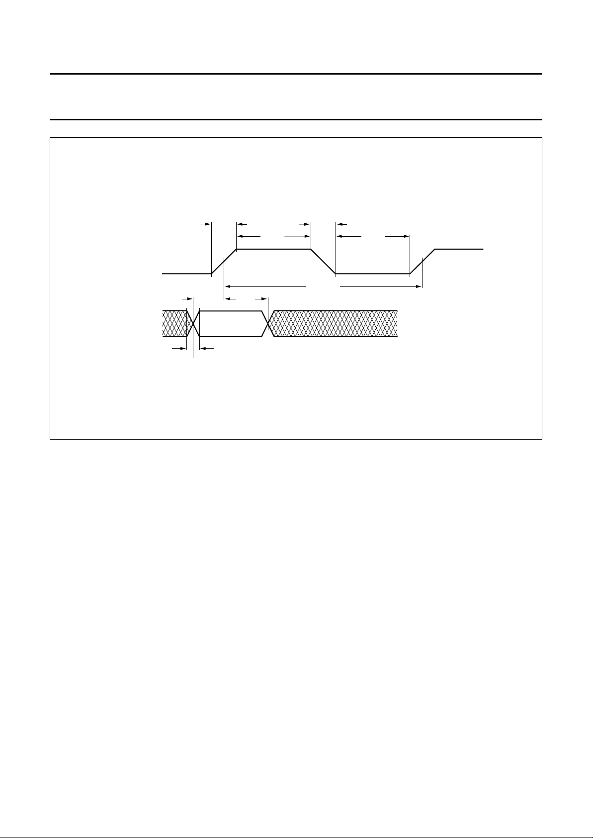
Philips Semiconductors Preliminary specification
MPEG-2 systems demultiplexer SAA7205H
handbook, full pagewidth
GPST
GPO7 to GPO0
GPSYNC
GPV
HSE
t
t
i(r)
i(r)(CLK)
t
i(su)
t
CLKH
T
t
i(h)a
t
i(f)
cy(CLK)
t
i(f)(CLK)
t
CLKL
Fig.32 Timing definition of the alternative asynchronous input interface signals.
MGG792
1997 Jan 21 67
Page 68
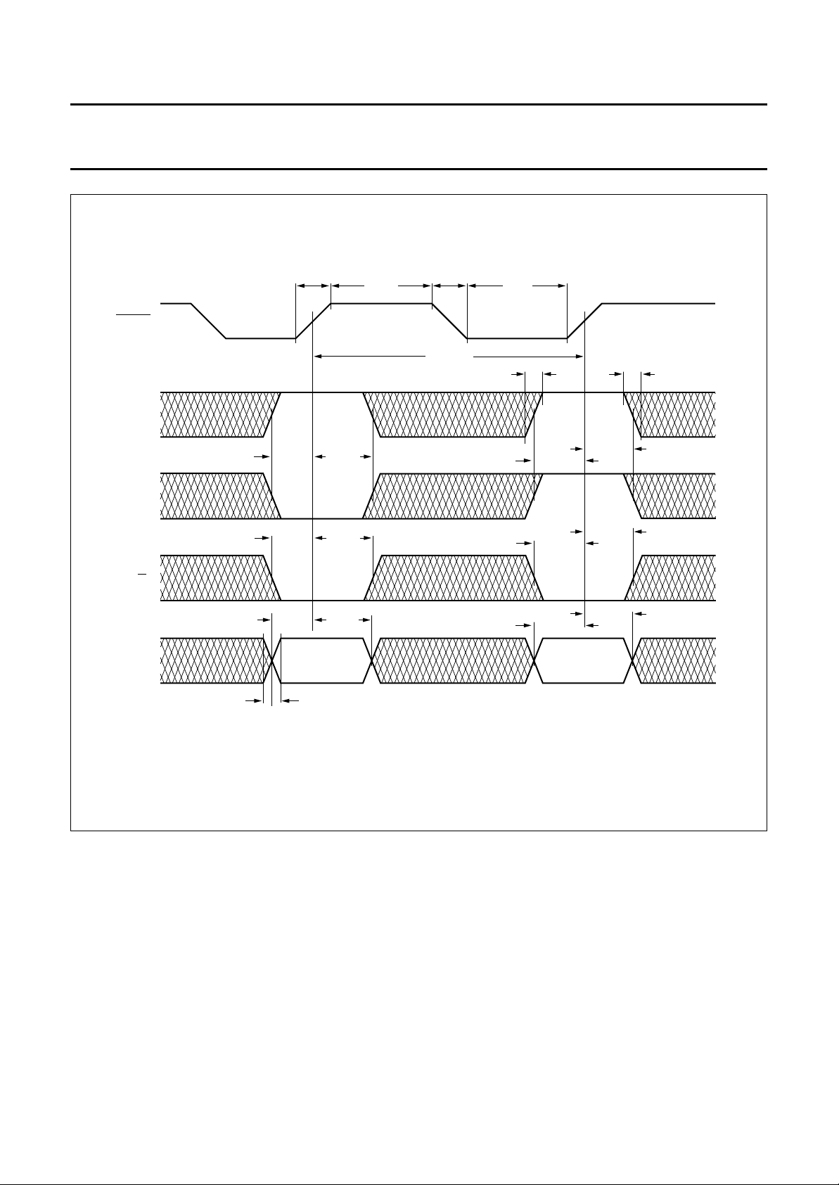
Philips Semiconductors Preliminary specification
MPEG-2 systems demultiplexer SAA7205H
handbook, full pagewidth
CSDEM
A1
A0
R/W
MDAT
t
i(su)(W)
t
i(su)(W)
t
i(su)(W)
t
r(CS)
MSB
t
i(h)(W)
t
i(h)(W)
t
i(h)(W)
t
CSH
t
f(CS)
T
cy(CS)
t
i(r)(W)
t
CSL
t
i(su)(W)
t
i(su)(W)
t
i(su)(W)
LSB
t
i(h)(W)
t
i(h)(W)
t
i(h)(W)
t
i(f)(W)
t
i(r)(W)
t
i(f)(W)
Fig.33 Timing definition of the microcontroller interface signals (address write cycle).
1997 Jan 21 68
MGG793
Page 69

Philips Semiconductors Preliminary specification
MPEG-2 systems demultiplexer SAA7205H
handbook, full pagewidth
CSDEM
A1
A0
R/W
MDAT
t
i(su)(W)
t
i(su)(W)
t
i(su)(W)
t
r(CS)
MSB
t
i(h)(W)
t
i(h)(W)
t
i(h)(W)
t
CSH
t
f(CS)
T
cy(CS)
t
i(f)(W)
t
CSL
t
i(su)(W)
t
i(su)(W)
t
i(su)(W)
LSB
t
i(h)(W)
t
i(h)(W)
t
i(h)(W)
t
i(r)(W)
t
i(r)(W)
t
i(f)(W)
Fig.34 Timing definition of the microcontroller interface signals (data write cycle).
MGG794
1997 Jan 21 69
Page 70
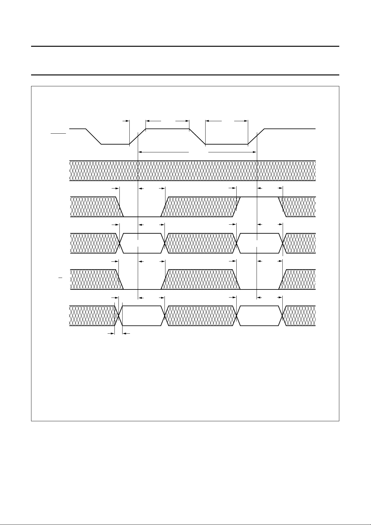
Philips Semiconductors Preliminary specification
MPEG-2 systems demultiplexer SAA7205H
handbook, full pagewidth
CSDEM
A1
A0
A2 to A9
R/W
i(h)(W)
i(h)(W)
i(h)(W)
i(h)(W)
t
CSH
t
f(CS)
T
cy(CS)
t
CSL
t
i(su)(W)
t
i(su)(W)
t
i(su)(W)
t
i(su)(W)
t
r(CS)
t
i(su)(W)
t
i(su)(W)
t
i(su)(W)
t
i(su)(W)
t
t
ADDRESS ADDRESS
t
t
t
i(h)(W)
t
i(h)(W)
t
i(h)(W)
t
i(h)(W)
MDAT
t
i(r)(W)
MSB
t
i(f)(W)
LSB
Fig.35 Timing definition of the microcontroller interface signals (data write cycle in direct addressing mode).
1997 Jan 21 70
MGG795
Page 71

Philips Semiconductors Preliminary specification
MPEG-2 systems demultiplexer SAA7205H
handbook, full pagewidth
CSDEM
A1
A0
R/W
MDAT
t
f(CS)
t
o(h)(R)
t
o(d)(R)
T
cy(CSL)(R)
t
i(su)(W)
t
o(d)(R)
t
o(h)(R)
MSB LSB
t
r(CS)
t
i(h)(W)
t
o(L-Z)
t
o(r)(R)
t
o(f)(R)
t
o(H-Z)
Fig.36 Timing definition of the microcontroller interface signals (read cycle).
MGG796
1997 Jan 21 71
Page 72

Philips Semiconductors Preliminary specification
MPEG-2 systems demultiplexer SAA7205H
handbook, full pagewidth
CSDEM
A1
A2 to A9
A0
R/W
t
f(CS)
t
i(su)(W)
t
i(h)(W)
ADDRESS ADDRESS
T
cy(CSL)(R)
t
i(su)(W)
t
i(h)(W)
t
i(su)(W)
t
r(CS)
t
i(h)(W)
t
o(r)(R)
t
o(d)(R2)
t
o(f)(R)
t
o(H-Z)
MGG797
MDAT
t
o(h)(R)
t
o(L-Z)
t
o(d)(R1)
t
o(h)(R)
MSB LSB
Fig.37 Timing definition of the microcontroller interface signals (read cycle in direct addressing mode).
1997 Jan 21 72
Page 73

Philips Semiconductors Preliminary specification
MPEG-2 systems demultiplexer SAA7205H
handbook, full pagewidth
DCLK
GPO7 to GPO0
HSV
HSYNC
HSE
Fig.38 Timing definition of the high speed data output interface signals.
t
r(CLKO)
t
CLKOH
t
f(CLKO)
t
o(h)h
T
cy(CLKO)
t
o(d)h
t
o(r)
t
CLKOL
t
o(f)
MGG798
handbook, full pagewidth
GPO7 to GPO0
GPSYNC
GPST
GPV
t
r(CLKO)
t
CLKOH
t
f(CLKO)
t
o(h)g
T
cy(CLKO)
t
o(d)g
t
Fig.39 Timing definition of the generic data filter output interface signals.
1997 Jan 21 73
o(r)
t
CLKOL
t
o(f)
MGG799
Page 74

Philips Semiconductors Preliminary specification
MPEG-2 systems demultiplexer SAA7205H
handbook, full pagewidth
VO7 to VO0
CLKP
t
f(CLKO)
t
t
o(d)p
t
o(r)
t
o(d)
r(CLKO)
t
o(f)
t
CLKOH
video or audio datavideo or audio data
T
cy(CLKO)
t
CLKOL
MGG800
Fig.40 Timing definition of the third party video output interface signals.
1997 Jan 21 74
Page 75

Philips Semiconductors Preliminary specification
MPEG-2 systems demultiplexer SAA7205H
k, full pagewidth
<360 µs
222 ns
>5 ns
<90 µs
<24 ns <24 ns <24 ns
MGG801
<17 ns>0 ns
See microcontroller timing definition of read write cycle
VSEL
R/W
MICRO-
CONTROLLER
PIN's CONTROL
MDAT7 to
MDAT0
1997 Jan 21 75
<24 ns
>222 ns
video data
Fig.41 Timing definition of the third party video read and write cycle interface signals.
CSVID
VO7 to VO0
Page 76

Philips Semiconductors Preliminary specification
MPEG-2 systems demultiplexer SAA7205H
handbook, full pagewidth
CCLKI
CLK13.5
CbREF
COMSYNC
HSYNC
VSYNC
EVEN/ODD
PWMO
handbook, full pagewidth
t
r(CCLK)
t
o(h)
t
o(f)
t
CCLKH
t
o(d) + 5
t
o(r)
T
cy(CCLK)
t
f(CCLK)
t
CCLKL
MGG802
Fig.42 Timing definition of the generic video interface signals in master mode.
t
r(CCLK)
t
CCLKH
t
f(CCLK)
t
CCLKL
CCLKI
VIN
CLK13.5
CbREF
COMSYNC
HSYNC
VSYNC
EVEN/ODD
PWMO
t
i(su)
t
i(f)
t
i(r)
t
o(h)
t
o(f)
t
i(h)
t
o(d) + 5
Fig.43 Timing definition of the generic video interface signals in slave mode.
1997 Jan 21 76
t
T
o(r)
cy(CCLK)
MGG803
Page 77

Philips Semiconductors Preliminary specification
MPEG-2 systems demultiplexer SAA7205H
handbook, full pagewidth
AUDECLK
AUDAT
AUDATV
AUE
t
r(CLKO)
111 ns + t
111 ns − t
o(h)
t
CLKOHa
o(d)
T
cy(CLKOa)
t
f(CLKO)
t
CLKOLa
Fig.44 Timing definition of audio decoders in normal mode (32 to 448 kHz).
MGG804
handbook, full pagewidth
AUDECLK
AUDAT
AUDATV
AUE
t
r(CLKO)
74 ns + t
74 ns − t
o(h)
t
CLKOHa
o(d)
T
cy(CLKOa)
Fig.45 Timing definition of audio decoders in SAA2500 mode (9 MHz).
1997 Jan 21 77
t
f(CLKO)
t
CLKOLa
MGG805
Page 78

Philips Semiconductors Preliminary specification
MPEG-2 systems demultiplexer SAA7205H
handbook, full pagewidth
handbook, full pagewidth
AUDATV
CCLKI
AUDECLK
CLKP
or
t
r(CCLK)
t
o(h)
t
CCLKH
t
o(d)
T
cy(CCLK)
t
f(CCLK)
t
CCLKL
Fig.46 Timing definition of audio decoders in gated clock mode.
T
cy(CLKO)
t
CLKOL
MGG806
111 + t
t
o(f)
o(d)
t
o(r)
VO7 to VO0
VSEL = 1.
VREQ (for video) = 0.
or
AREQ (for audio) = 0.
111 − t
o(h)
Fig.47 Timing definition of the combined audio/video output interface signals.
1997 Jan 21 78
video or audio datavideo or audio data
MGG807
Page 79

Philips Semiconductors Preliminary specification
MPEG-2 systems demultiplexer SAA7205H
handbook, full pagewidth
handbook, full pagewidth
TTC
TTD
t
r(CLKO)
t
CLKOHtt
t
o(h)tt
t
f(CLKO)
T
cy(CLKOtt)
t
o(d)tt
t
CLKOLtt
Fig.48 Timing definition of the teletext decoders.
T
cy(W)
MGG808
OERAM
t
su(OE-RAMA)
RAMA14 to
RAMA0
WERAM
RAMIO7 to
RAMIO0
t
su(A)
t
AV
t
W
t
su(D-W)
Fig.49 Timing definition of the SRAM interface write cycle.
1997 Jan 21 79
t
h(A)
t
h(D-W)
t
dat(Z-OE)
MGG809
Page 80

Philips Semiconductors Preliminary specification
MPEG-2 systems demultiplexer SAA7205H
handbook, full pagewidth
OERAM
RAMA14 to RAMA0
RAMIO7 to RAMIO0
t
su(WE-OE)
t
su(A-OE)
T
cy(R)
t
d(DAT)(h)
MGG810
Fig.50 Timing definition of the SRAM interface read cycle.
13 APPENDIX Table 14 Parser states
STATE NUMBER STATE NAME MPEG-2 FIELD SIZE (BITS)
1 reset indefinite
2 sync 8
3 indicators 16
4 flag_n_continuity 8
5 adaption_field/af_length 8
6 adaption_field/flags 8
7 adaption_field/prg_clk_ref 48
8 adaption_field/org_prg_clk_ref 48
9 adaption_field/private_segment 8K
10 adaption_field/splice_countdown 8
11 adaption_field/af_extension 8K
12 adaption_field/af_stuffing 8K
1997 Jan 21 80
Page 81

Philips Semiconductors Preliminary specification
MPEG-2 systems demultiplexer SAA7205H
14 PACKAGE OUTLINE
QFP128: plastic quad flat package;
128 leads (lead length 1.6 mm); body 28 x 28 x 3.4 mm; high stand-off height
c
y
96 65
97
X
A
64
Z
E
SOT320-2
pin 1 index
128
1
w M
b
0.25
p
D
H
D
D
0.45
0.23
0.13
28.1
27.9
0.30
e
DIMENSIONS (mm are the original dimensions)
mm
A
max.
3.95
0.40
0.25
3.70
3.15
UNIT A1A2A3bpcE
32
Z
D
0 5 10 mm
(1) (1)(1)
(1)
28.1
27.9
e
H
E
w M
b
p
33
v M
A
B
v M
B
scale
eH
H
D
31.45
0.8
30.95
LLpQZywv θ
E
31.45
30.95
E
0.95
0.65
1.70
1.55
A
1
detail X
0.20.3 0.11.6
A
2
A
Q
(A )
3
θ
L
p
L
Z
E
D
1.8
1.4
o
7
o
0
1.8
1.4
Note
1. Plastic or metal protrusions of 0.25 mm maximum per side are not included.
OUTLINE
VERSION
SOT320-2
IEC JEDEC EIAJ
REFERENCES
1997 Jan 21 81
EUROPEAN
PROJECTION
ISSUE DATE
95-02-04
96-03-14
Page 82

Philips Semiconductors Preliminary specification
MPEG-2 systems demultiplexer SAA7205H
15 SOLDERING
15.1 Introduction
There is no soldering method that is ideal for all IC
packages. Wave soldering is often preferred when
through-hole and surface mounted components are mixed
on one printed-circuit board. However, wave soldering is
not always suitable for surface mounted ICs, or for
printed-circuits with high population densities. In these
situations reflow soldering is often used.
This text gives a very brief insight to a complex technology.
A more in-depth account of soldering ICs can be found in
our
“IC Package Databook”
15.2 Reflow soldering
Reflow soldering techniques are suitable for all QFP
packages.
The choice of heating method may be influenced by larger
plastic QFP packages (44 leads, or more). If infrared or
vapour phase heating is used and the large packages are
not absolutely dry (less than 0.1% moisture content by
weight), vaporization of the small amount of moisture in
them can cause cracking of the plastic body. For more
information, refer to the Drypack chapter in our
Reference Handbook”
Reflow soldering requires solder paste (a suspension of
fine solder particles, flux and binding agent) to be applied
to the printed-circuit board by screen printing, stencilling or
pressure-syringe dispensing before package placement.
Several techniques exist for reflowing; for example,
thermal conduction by heated belt. Dwell times vary
between 50 and 300 seconds depending on heating
method. Typical reflow temperatures range from
215 to 250 °C.
Preheating is necessary to dry the paste and evaporate
the binding agent. Preheating duration: 45 minutes at
45 °C.
(order code 9398 652 90011).
“Quality
(order code 9397 750 00192).
15.3 Wave soldering
Wave soldering is not recommended for QFP packages.
This is because of the likelihood of solder bridging due to
closely-spaced leads and the possibility of incomplete
solder penetration in multi-lead devices.
If wave soldering cannot be avoided, the following
conditions must be observed:
• A double-wave (a turbulent wave with high upward
pressure followed by a smooth laminar wave)
soldering technique should be used.
• The footprint must be at an angle of 45° to the board
direction and must incorporate solder thieves
downstream and at the side corners.
Even with these conditions, do not consider wave
soldering the following packages: QFP52 (SOT379-1),
QFP100 (SOT317-1), QFP100 (SOT317-2),
QFP100 (SOT382-1) or QFP160 (SOT322-1).
During placement and before soldering, the package must
be fixed with a droplet of adhesive. The adhesive can be
applied by screen printing, pin transfer or syringe
dispensing. The package can be soldered after the
adhesive is cured.
Maximum permissible solder temperature is 260 °C, and
maximum duration of package immersion in solder is
10 seconds, if cooled to less than 150 °C within
6 seconds. Typical dwell time is 4 seconds at 250 °C.
A mildly-activated flux will eliminate the need for removal
of corrosive residues in most applications.
15.4 Repairing soldered joints
Fix the component by first soldering two diagonallyopposite end leads. Use only a low voltage soldering iron
(less than 24 V) applied to the flat part of the lead. Contact
time must be limited to 10 seconds at up to 300 °C. When
using a dedicated tool, all other leads can be soldered in
one operation within 2 to 5 seconds between
270 and 320 °C.
1997 Jan 21 82
Page 83

Philips Semiconductors Preliminary specification
MPEG-2 systems demultiplexer SAA7205H
16 DEFINITIONS
Data sheet status
Objective specification This data sheet contains target or goal specifications for product development.
Preliminary specification This data sheet contains preliminary data; supplementary data may be published later.
Product specification This data sheet contains final product specifications.
Limiting values
Limiting values given are in accordance with the Absolute Maximum Rating System (IEC 134). Stress above one or
more of the limiting values may cause permanent damage to the device. These are stress ratings only and operation
of the device at these or at any other conditions above those given in the Characteristics sections of the specification
is not implied. Exposure to limiting values for extended periods may affect device reliability.
Application information
Where application information is given, it is advisory and does not form part of the specification.
17 LIFE SUPPORT APPLICATIONS
These products are not designed for use in life support appliances, devices, or systems where malfunction of these
products can reasonably be expected to result in personal injury. Philips customers using or selling these products for
use in such applications do so at their own risk and agree to fully indemnify Philips for any damages resulting from such
improper use or sale.
1997 Jan 21 83
Page 84

Philips Semiconductors – a worldwide company
Argentina: see South America
Australia: 34 Waterloo Road, NORTH RYDE, NSW 2113,
Tel. +61 2 9805 4455, Fax. +61 2 9805 4466
Austria: Computerstr. 6, A-1101 WIEN, P.O. Box 213,
Tel. +43 1 60 101, Fax. +43 1 60 101 1210
Belarus: Hotel Minsk Business Center, Bld. 3, r. 1211, Volodarski Str. 6,
220050 MINSK, Tel. +375 172 200 733, Fax. +375 172 200 773
Belgium: see The Netherlands
Brazil: see South America
Bulgaria: Philips Bulgaria Ltd., Energoproject, 15th floor,
51 James Bourchier Blvd., 1407 SOFIA,
Tel. +359 2 689 211, Fax. +359 2 689 102
Canada: PHILIPS SEMICONDUCTORS/COMPONENTS,
Tel. +1 800 234 7381
China/Hong Kong: 501 Hong Kong Industrial Technology Centre,
72 Tat Chee Avenue, Kowloon Tong, HONG KONG,
Tel. +852 2319 7888, Fax. +852 2319 7700
Colombia: see South America
Czech Republic: see Austria
Denmark: Prags Boulevard 80, PB 1919, DK-2300 COPENHAGEN S,
Tel. +45 32 88 2636, Fax. +45 31 57 1949
Finland: Sinikalliontie 3, FIN-02630 ESPOO,
Tel. +358 9 615800, Fax. +358 9 61580/xxx
France: 4 Rue du Port-aux-Vins, BP317, 92156 SURESNES Cedex,
Tel. +33 1 40 99 6161, Fax. +33 1 40 99 6427
Germany: Hammerbrookstraße 69, D-20097 HAMBURG,
Tel. +49 40 23 53 60, Fax. +49 40 23 536 300
Greece: No. 15, 25th March Street, GR 17778 TAVROS/ATHENS,
Tel. +30 1 4894 339/239, Fax. +30 1 4814 240
Hungary: see Austria
India: Philips INDIA Ltd, Shivsagar Estate, A Block, Dr. Annie Besant Rd.
Worli, MUMBAI 400 018, Tel. +91 22 4938 541, Fax. +91 22 4938 722
Indonesia: see Singapore
Ireland: Newstead, Clonskeagh, DUBLIN 14,
Tel. +353 1 7640 000, Fax. +353 1 7640 200
Israel: RAPAC Electronics, 7 Kehilat Saloniki St, TEL AVIV 61180,
Tel. +972 3 645 0444, Fax. +972 3 649 1007
Italy: PHILIPS SEMICONDUCTORS, Piazza IV Novembre 3,
20124 MILANO, Tel. +39 2 6752 2531, Fax. +39 2 6752 2557
Japan: Philips Bldg 13-37, Kohnan 2-chome, Minato-ku, TOKYO 108,
Tel. +81 3 3740 5130, Fax. +81 3 3740 5077
Korea: Philips House, 260-199 Itaewon-dong, Yongsan-ku, SEOUL,
Tel. +82 2 709 1412, Fax. +82 2 709 1415
Malaysia: No. 76 Jalan Universiti, 46200 PETALING JAYA, SELANGOR,
Tel. +60 3 750 5214, Fax. +60 3 757 4880
Mexico: 5900 Gateway East, Suite 200, EL PASO, TEXAS 79905,
Tel. +9-5 800 234 7381
Middle East: see Italy
Netherlands: Postbus 90050, 5600 PB EINDHOVEN, Bldg. VB,
Tel. +31 40 27 82785, Fax. +31 40 27 88399
New Zealand: 2 Wagener Place, C.P.O. Box 1041, AUCKLAND,
Tel. +64 9 849 4160, Fax. +64 9 849 7811
Norway: Box 1, Manglerud 0612, OSLO,
Tel. +47 22 74 8000, Fax. +47 22 74 8341
Philippines: Philips Semiconductors Philippines Inc.,
106 Valero St. Salcedo Village, P.O. Box 2108 MCC, MAKATI,
Metro MANILA, Tel. +63 2 816 6380, Fax. +63 2 817 3474
Poland: Ul. Lukiska 10, PL 04-123 WARSZAWA,
Tel. +48 22 612 2831, Fax. +48 22 612 2327
Portugal: see Spain
Romania: see Italy
Russia: Philips Russia, Ul. Usatcheva 35A, 119048 MOSCOW,
Tel. +7 095 755 6918, Fax. +7 095 755 6919
Singapore: Lorong 1, Toa Payoh, SINGAPORE 1231,
Tel. +65 350 2538, Fax. +65 251 6500
Slovakia: see Austria
Slovenia: see Italy
South Africa: S.A. PHILIPS Pty Ltd., 195-215 Main Road Martindale,
2092 JOHANNESBURG, P.O. Box 7430 Johannesburg 2000,
Tel. +27 11 470 5911, Fax. +27 11 470 5494
South America: Rua do Rocio 220, 5th floor, Suite 51,
04552-903 São Paulo, SÃO PAULO - SP, Brazil,
Tel. +55 11 821 2333, Fax. +55 11 829 1849
Spain: Balmes 22, 08007 BARCELONA,
Tel. +34 3 301 6312, Fax. +34 3 301 4107
Sweden: Kottbygatan 7, Akalla, S-16485 STOCKHOLM,
Tel. +46 8 632 2000, Fax. +46 8 632 2745
Switzerland: Allmendstrasse 140, CH-8027 ZÜRICH,
Tel. +41 1 488 2686, Fax. +41 1 481 7730
Taiwan: Philips Semiconductors, 6F, No. 96, Chien Kuo N. Rd., Sec. 1,
TAIPEI, Taiwan Tel. +886 2 2134 2870, Fax. +886 2 2134 2874
Thailand: PHILIPS ELECTRONICS (THAILAND) Ltd.,
209/2 Sanpavuth-Bangna Road Prakanong, BANGKOK 10260,
Tel. +66 2 745 4090, Fax. +66 2 398 0793
Turkey: Talatpasa Cad. No. 5, 80640 GÜLTEPE/ISTANBUL,
Tel. +90 212 279 2770, Fax. +90 212 282 6707
Ukraine: PHILIPS UKRAINE, 4 Patrice Lumumba str., Building B, Floor 7,
252042 KIEV, Tel. +380 44 264 2776, Fax. +380 44 268 0461
United Kingdom: Philips Semiconductors Ltd., 276 Bath Road, Hayes,
MIDDLESEX UB3 5BX, Tel. +44 181 730 5000, Fax. +44 181 754 8421
United States: 811 East Arques Avenue, SUNNYVALE, CA 94088-3409,
Tel. +1 800 234 7381
Uruguay: see South America
Vietnam: see Singapore
Yugoslavia: PHILIPS, Trg N. Pasica 5/v, 11000 BEOGRAD,
Tel. +381 11 625 344, Fax.+381 11 635 777
For all other countries apply to: Philips Semiconductors, Marketing & Sales Communications,
Building BE-p, P.O. Box 218, 5600 MD EINDHOVEN, The Netherlands, Fax. +31 40 27 24825
© Philips Electronics N.V. 1997 SCA53
All rights are reserved. Reproduction in whole or in part is prohibited without the prior written consent of the copyright owner.
The information presented in this document does not form part of any quotation or contract, is believed to be accurate and reliable and may be changed
without notice. No liability will be accepted by the publisher for any consequence of its use. Publication thereof does not convey nor imply any license
under patent- or other industrial or intellectual property rights.
Internet: http://www.semiconductors.philips.com
Printed in The Netherlands 547047/1200/01/pp84 Date of release: 1997 Jan 21 Document order number: 9397 750 00924
 Loading...