

Page 1

DATA SH EET
Preliminary specification
Supersedes data of 1996 Sep 11
File under Integrated Circuits, IC22
1996 Oct 02
INTEGRATED CIRCUITS
SAA7182A; SAA7183A
Digital Video Encoder
(EURO-DENC2)
Page 2

1996 Oct 02 2
Philips Semiconductors Preliminary specification
Digital Video Encoder (EURO-DENC2) SAA7182A; SAA7183A
FEATURES
• Monolithic CMOS 3.3 V device with 5 V input stages
• Digital PAL/NTSC/SECAM encoder
• System pixel frequency 13.5 MHz
• Accepts MPEG decoded data on 8-bit wide input port.
Input data format Cb, Y, Cr etc. “
(CCIR 656)
” or
Y and Cb, Cr on 16 lines
• Three DACs for CVBS, Y and C operating at 27 MHz
with 10 bit resolution
• Three DACs for RGB operating at 27 MHz with 9 bit
resolution, RGB sync on CVBS and Y
• Analog multiplexing between internal RGB and external
RGB on-chip
• CVBS, Y, C and RGB output simultaneously
• Closed captioning and teletext encoding including
sequencer and filter
• Line 23 wide screen signalling encoding
• On-chip Cr, Y, Cb to RGB dematrix, including gain
adjustment for Y and Cr, Cb, optionally to be by-passed
for Cr, Y, Cb output on RGB DACs
• Fast I
2
C-bus control port (400 kHz)
• Encoder can be master or slave
• Programmable horizontal and vertical input
synchronization phase
• Programmable horizontal sync output phase
• Internal Colour Bar Generator (CBG)
• Overlay with Look-Up Tables (LUTs) 8 × 3 bytes
• Macrovision Pay-per-View copy protection system as
option, also used for RGB output.
This applies to SAA7183A only. The device is protected
by USA patent numbers 4631603, 4577216 and
4819098 and other intellectual property rights. Use of
the Macrovision anti-copy process in the device is
licensed for non-commercial home use only.
Reverse engineering or disassembly is prohibited.
Please contact your nearest Philips Semiconductor
sales office for more information
• Controlled rise/fall times of output syncs and blanking
• Down-mode of DACs
• PQFP80 or PLCC84 package.
GENERAL DESCRIPTION
The SAA7182A; SAA7183A encodes digital YUV video
data to an NTSC, PAL, SECAM CVBS or S-Video signal
and also RGB.
Optionally, the YUV to RGB dematrix can be by-passed
providing the digital-to-analog converted Cb, Y, Cr signals
instead of RGB.
The circuit accepts CCIR compatible YUV data with
720 active pixels per line in 4:2:2multiplexed formats,
for example MPEG decoded data. It includes a sync/clock
generator and on-chip Digital-to-Analog Converters
(DACs).
The circuit is compatible to the DIG-TV2 chip family.
ORDERING INFORMATION
TYPE
NUMBER
PACKAGE
NAME DESCRIPTION VERSION
SAA7182AWP;
SAA7183AWP
PLCC84 plastic leaded chip carrier; 84 leads SOT189-2
QFP80 plastic quad flat package; 80 leads (lead length 1.95 mm);
body 14 × 20 × 2.8 mm
SOT318-2
Page 3

1996 Oct 02 3
Philips Semiconductors Preliminary specification
Digital Video Encoder (EURO-DENC2) SAA7182A; SAA7183A
QUICK REFERENCE DATA
SYMBOL PARAMETER MIN. TYP. MAX. UNIT
V
DDA3
3.3 V analog supply voltage 3.1 3.3 3.5 V
V
DDD3
3.3 V digital supply voltage 3.0 3.3 3.6 V
V
DDD5
5 V digital supply voltage 4.75 5.0 5.25 V
I
DDA
analog supply current −−110 mA
I
DDD3
3.3 V digital supply current −−80 mA
I
DDD5
5 V digital supply current −−10 mA
V
i
input signal voltage levels TTL compatible
V
o(p-p)
analog output signal voltages Y, C, CVBS and RGB without load
(peak-to-peak value)
− 1.4 − V
R
L
load resistance 75 − 300 Ω
ILE LF integral linearity error −−±2 LSB
DLE LF differential linearity error −−±1 LSB
T
amb
operating ambient temperature 0 − +70 °C
Page 4

1996 Oct 02 4
Philips Semiconductors Preliminary specification
Digital Video Encoder (EURO-DENC2) SAA7182A; SAA7183A
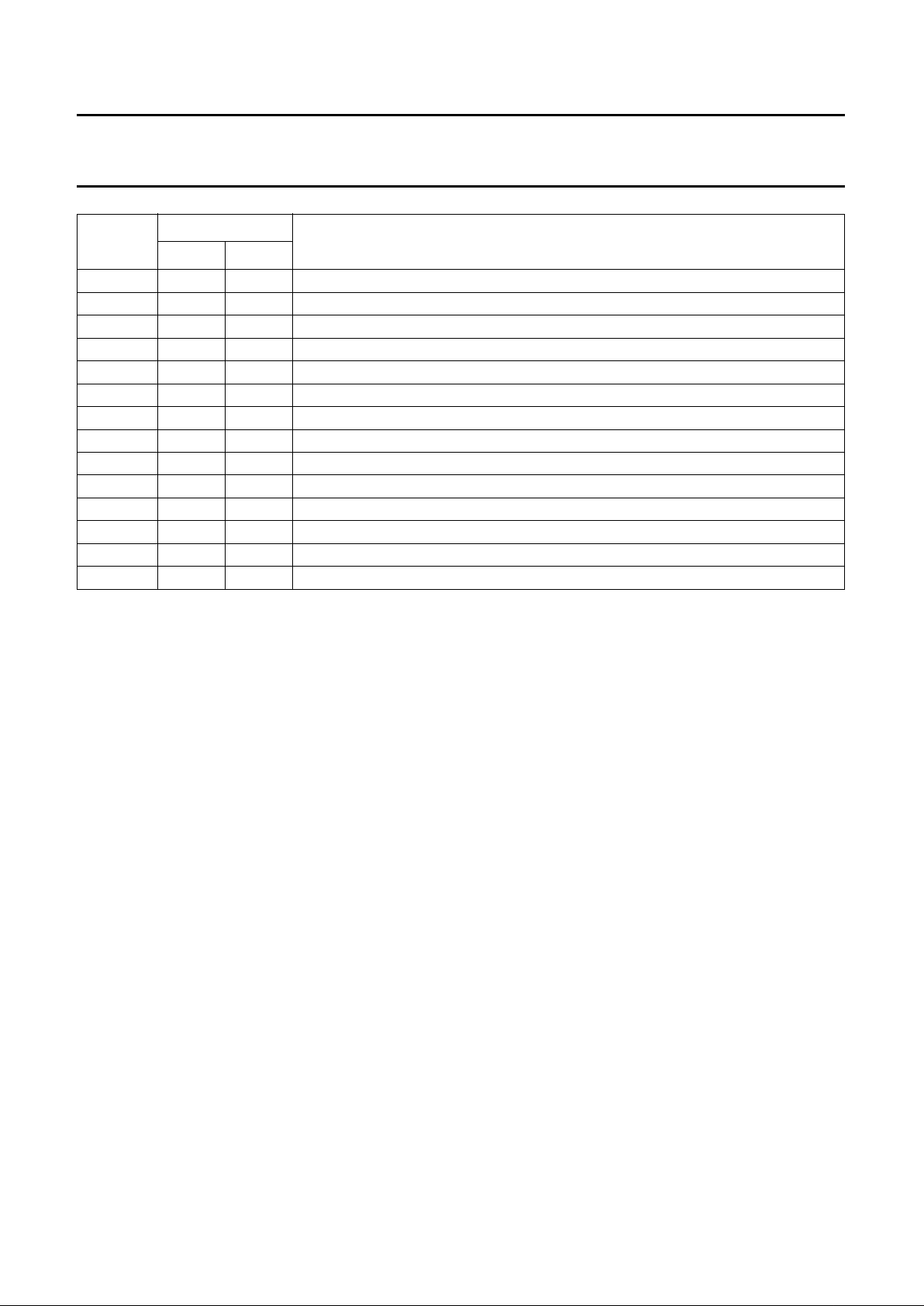
BLOCK DIAGRAM
Fig.1 Block diagram; PLCC84.
handbook, full pagewidth
I2C-BUS
INTERFACE
DATA
MANAGER
SECAM
PROCESSOR
ENCODER
SYNC
CLOCK
OUTPUT
INTERFACE
D
A
RGB
PROCESSOR
D
A
184834
50 35 36 20 47 45
44 48
75
63, 64,
68, 70,
72, 74
37
DP0
to
DP7
MP7
to
MP0
KEY
TTX
OVL2
to
OVL0
3, 15, 24,
30, 39, 42,
51, 79, 81
5, 14, 22,
29, 38, 46,
49, 80, 82
2, 23, 40, 41,
43, 66
78 77
59 56
54,
57, 60
73
71
69
52, 67, 76
65
53
62
61
58
55
RESET SDA SCL
RTCI
CDIR
RCV1
RCV2
TTXRQ
CREF
XTALO
XTALI
LLC
TESTB
V
DDA4
to V
DDA9
SA
CVBS
Y
CHROMA
V
SSA1
to
V
SSA3
TESTC
SELI
RI
RED
GREEN
BLUE
I2C-bus
control
I2C-bus
control
I
2
C-bus
control
I
2
C-bus
control
I
2
C-bus
control
I
2
C-bus
control
I
2
C-bus
control
DbDr
8
V
SSD1
to
V
SSD9
V
DDD1
to
V
DDD9
V
DDA1
to
V
DDA3
n.c.
SP AP
GI
BI
internal
control bus
clock
and timing
8
8
8
8
3
8
8
8
Y
Y
C
CbCr
Y
CbCr
3
21
9
10 to 13
16 to 19
25 to 28
31 to 34
6 to 8
SAA7182A
SAA7183A
MGD668
Page 5

1996 Oct 02 5
Philips Semiconductors Preliminary specification
Digital Video Encoder (EURO-DENC2) SAA7182A; SAA7183A
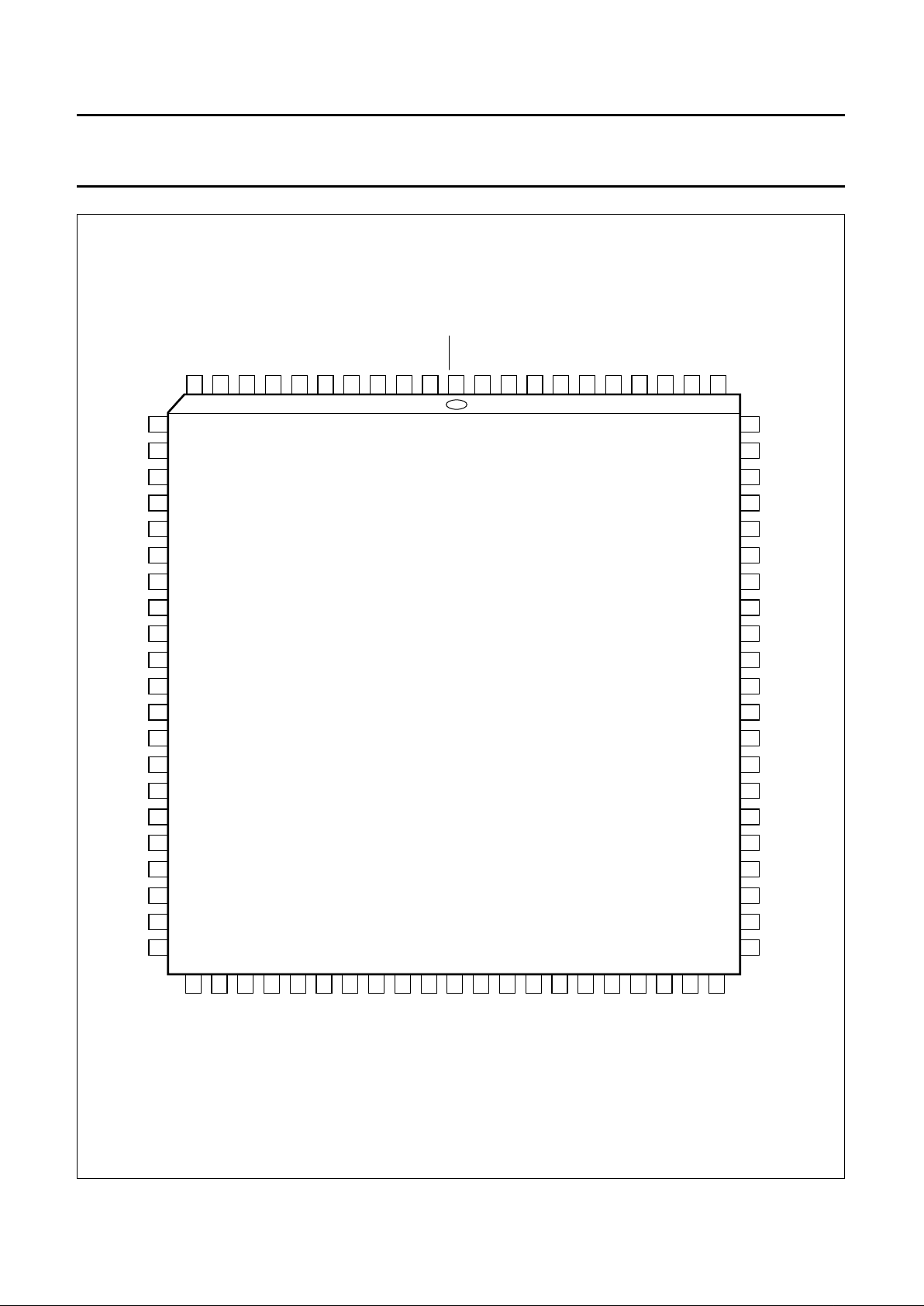
Fig.2 Block diagram; QFP80.
andbook, full pagewidth
I2C-BUS
INTERFACE
DATA
MANAGER
SECAM
PROCESSOR
ENCODER
SYNC
CLOCK
OUTPUT
INTERFACE
D
A
RGB
PROCESSOR
D
A
73 72 71 75
38 25 26 11 35 33
32 36
63
52, 53,
56, 58,
60, 62
27
KEY
TTX
6, 14, 20,
29, 31, 39,
67, 69, 74
5, 13, 19,
28, 34, 37,
68, 70, 76 30, 40
66 65
48 45
43,
46, 49
61
59
57
41, 55, 64
54
42
51
50
47
44
RESET SDA SCL
RTCI
CDIR
RCV1
RCV2
TTXRQ
CREF
XTALO
XTALI
LLC
TESTB
V
DDA4
to V
DDA9
SA
CVBS
Y
CHROMA
TESTC
SELI
RI
RED
GREEN
BLUE
I2C-bus
control
I2C-bus
control
I
2
C-bus
control
I
2
C-bus
control
I
2
C-bus
control
I
2
C-bus
control
I
2
C-bus
control
DbDr
8
V
SSD1
to
V
SSD9
V
DDD1
to
V
DDD9
V
DDA1
to
V
DDA3
n.c.
SP AP
GI
BI
internal
control bus
clock
and timing
8
8
8
8
3
8
8
8
Y
Y
C
CbCr
Y
CbCr
3
12
80
1 to 4
7 to 10
15 to 18
21 to 24
77 to 79
SAA7182A
SAA7183A
MGD670
DP0
to
DP7
MP7
to
MP0
OVL2
to
OVL0
V
SSA1
to
V
SSA3
Page 6

1996 Oct 02 6
Philips Semiconductors Preliminary specification
Digital Video Encoder (EURO-DENC2) SAA7182A; SAA7183A
PINNING
SYMBOL
PIN
DESCRIPTION
PLCC84 QFP80
RESET 1 73 Reset input, active LOW. After reset is applied, all digital I/Os are in input mode.
The I2C-bus receiver waits for the START condition.
n.c. 2 − not connected
V
SSD1
3 6 digital ground 1
SA 4 75 The I
2
C-bus slave address select input pin. LOW: slave address = 88H,
HIGH = 8CH.
V
DDD1
5 13 digital supply voltage 1 (3.3 V)
OVL2 6 77
3-bit overlay data input. This is the index for the internal look-up table.OVL1 7 78
OVL0 8 79
KEY 9 80 Key input for OVL. When HIGH it selects OVL input.
DP0 10 1
Lower 4 bits of the data port. Input for multiplexed Cb, Cr data if 16 line input mode
is used.
DP1 11 2
DP2 12 3
DP3 13 4
V
DDD2
14 5 digital supply voltage 2 (5 V)
V
SSD2
15 14 digital ground 2
DP4 16 7
Upper 4 bits of the data port. Input for multiplexed Cb, Cr data if 16 line input mode
is used.
DP5 17 8
DP6 18 9
DP7 19 10
TTXRQ 20 11 Teletext request output, indicating when bit stream is valid.
TTX 21 12 Teletext bit stream input.
V
DDD3
22 28 digital supply voltage 3 (3.3 V)
n.c. 23 − not connected
V
SSD3
24 20 digital ground 1
MP7 25 15
Upper 4 bits of MPEG port. It is an input for “
CCIR 656
” style multiplexed Cb, Y, Cr
data, or for Y data only, if 16 line input mode is used.
MP6 26 16
MP5 27 17
MP4 28 18
V
DDD4
29 19 digital supply voltage 4 (5 V)
V
SSD4
30 29 digital ground 4
MP3 31 21
Lower 4 bits of MPEG port. It is an input for “
CCIR 656
” style multiplexed Cb, Y, Cr
data, or for Y data only, if 16 line input mode is used.
MP2 32 22
MP1 33 23
MP0 34 24
RCV1 35 25 Raster Control 1 for video port. This pin receives/provides a VS/FS/FSEQ signal.
RCV2 36 26 Raster Control 2 for video port. This pin provides an HS pulse of programmable
length or receives an HS pulse.
Page 7

1996 Oct 02 7
Philips Semiconductors Preliminary specification
Digital Video Encoder (EURO-DENC2) SAA7182A; SAA7183A
RTCI 37 27 Real Time Control input. If the LLC clock is provided by an SAA7111 or SAA7151B,
RTCI should be connected to the RTCO pin of the respective decoder to improve
the signal quality.
V
DDD5
38 68 digital supply voltage 5 (3.3 V)
V
SSD5
39 39 digital ground 5
n.c. 40 40 not connected
n.c. 41 − not connected
V
SSD6
42 31 digital ground 6 for oscillator
n.c. 43 30 not connected
XTALI 44 32 Crystal oscillator input (from crystal). If the oscillator is not used, this pin should be
connected to ground.
XTALO 45 33 Crystal oscillator output (to crystal).
V
DDD6
46 34 digital supply voltage 6 for oscillator (3.3 V)
CREF 47 35 Clock Reference signal. This is the clock qualifier for DIG-TV2 compatible signals.
LLC 48 36 Line-Locked Clock. This is the 27 MHz master clock for the encoder. The I/O
direction is set by the CDIR pin.
V
DDD7
49 37 digital supply voltage 7 (5 V)
CDIR 50 38 Clock direction. If CDIR input is HIGH, the circuit receives a clock and optional
CREF signal, otherwise if CDIR is LOW, CREF and LLC are generated by the
internal crystal oscillator.
V
SSD7
51 67 digital ground 7
V
SSA1
52 41 Analog ground 1 for the DACs.
TESTC 53 42 Analog test pin. Leave open-circuit for normal operation.
V
DDA1
54 43 Analog supply voltage 1 for the RGB DACs (3.3 V).
BLUE 55 44 Analog output of the BLUE component.
BI 56 45 Analog input that can be switched to BLUE when SELI = HIGH.
V
DDA2
57 46 Analog supply voltage 2 for RGB DACs (3.3 V).
GREEN 58 47 Analog output of GREEN component.
GI 59 48 Analog input that can be switched to GREEN when SELI = HIGH.
V
DDA3
60 49 Analog supply voltage 3 for RGB DACs (3.3 V).
RED 61 50 Analog output of RED component.
RI 62 51 Analog input that can be switched to RED when SELI = HIGH.
V
DDA4
63 52 Analog supply voltage 4 for DACs (3.3 V).
V
DDA5
64 53 Analog supply voltage 5 for DACs (3.3 V).
SELI 65 54 Select analog input. Digital-to-analog converted RGB output when SELI = LOW;
RI, GI and BI output when SELI = HIGH.
n.c. 66 − not connected
V
SSA2
67 55 Analog ground 2 for the DACs.
V
DDA6
68 56 Analog supply voltage 6 for DACs (3.3 V).
CHROMA 69 57 Analog output of the chrominance signal.
V
DDA7
70 58 Analog supply voltage 7 for the Y/C/CVBS DACs (3.3 V).
SYMBOL
PIN
DESCRIPTION
PLCC84 QFP80
Page 8
1996 Oct 02 8
Philips Semiconductors Preliminary specification
Digital Video Encoder (EURO-DENC2) SAA7182A; SAA7183A
Y 71 59 Analog output of VBS signal.
V
DDA8
72 60 Analog supply voltage 8 for the Y/C/CVBS DACs.
CVBS 73 61 Analog output of the CVBS signal.
V
DDA9
74 62 Analog supply voltage 9 for the Y/C/CVBS DACs.
TESTB 75 63 Analog test pin. Leave open-circuit for normal operation.
V
SSA3
76 64 Analog ground 3 for the DACs.
AP 77 65 Test pin. Connected to digital ground for normal operation.
SP 78 66 Test pin. Connected to digital ground for normal operation.
V
SSD8
79 69 digital ground 8
V
DDD8
80 76 digital supply voltage 8 (3.3 V)
V
SSD9
81 74 digital ground 9
V
DDD9
82 70 digital supply voltage 9 (5 V)
SCL 83 71 I
2
C-bus serial clock input.
SDA 84 72 I
2
C-bus serial data input/output.
SYMBOL
PIN
DESCRIPTION
PLCC84 QFP80
Page 9
1996 Oct 02 9
Philips Semiconductors Preliminary specification
Digital Video Encoder (EURO-DENC2) SAA7182A; SAA7183A
Fig.3 Pin configuration; PLCC84.
handbook, full pagewidth
SAA7182A
SAA7183A
MGD669
12DP2
DP3
V
DDD2
V
SSD2
DP4
DP5
DP6
DP7
TTXRQ
TTX
V
DDD3
n.c.
V
SSD3
MP7
MP6
MP5
MP4
V
DDD4
V
SSD4
MP3
MP2
V
DDA9
CVBS
V
DDA8
Y
V
DDA7
CHROMA
V
DDA6
V
SSA2
n.c.
SELI
V
DDA5
V
DDA4
RI
RED
V
DDA3
GI
GREEN
V
DDA2
BI
BLUE
V
DDA1
MP1
MP0
RCV1
RCV2
RTCI
V
DDD5
V
SSD5
n.c.
n.c.
V
SSD6
n.c.
XTALI
XTALO
V
DDD6
CREF
LLC
V
DDD7
CDIR
V
SSD7
V
SSA1
TESTC
DP1
DP0
KEY
OVL0
OVL1
OVL2
V
DDD1
SA
V
SSD1
n.c.
RESET
SDA
SCL
V
DDD9VSSD9VDDD8VSSD8
SP
AP
V
SSA3
TESTB
13
14
15
16
17
18
19
20
21
22
23
24
25
26
27
28
29
30
31
32
74
73
72
71
70
69
68
67
66
65
64
63
62
61
60
59
58
57
56
55
54
33
34
35
36
37
38
39
40
41
42
43
44
45
46
47
48
49
50
51
52
53
11
10
9
8
7
6
5
4
3
2
1
84
83
82
81
80
79
78
77
76
75
Page 10
1996 Oct 02 10
Philips Semiconductors Preliminary specification
Digital Video Encoder (EURO-DENC2) SAA7182A; SAA7183A
Fig.4 Pin configuration; QFP80.
handbook, full pagewidth
SAA7182A
SAA7183A
MGD671
1
2
3
4
5
6
7
8
9
10
11
12
13
14
15
16
17
18
19
20
60
59
58
57
56
64
63
62
61
55
54
53
52
51
50
49
48
47
46
45
44
43
42
41
V
DDA8
Y
V
DDA7
CHROMA
V
DDA6
V
SSA3
TESTB
V
DDA9
CVBS
V
SSA2
SELI
V
DDA5
V
DDA4
RI
RED
V
DDA3
GI
GREEN
V
DDA2
BI
BLUE
V
DDA1
TESTC
V
SSA1
V
DDD2
V
SSD1
DP4
DP5
DP6
DP0
DP1
DP2
DP3
DP7
TTXRQ
TTX
V
DDD1
V
SSD2
MP7
MP6
MP5
MP4
V
DDD4
V
SSD3
MP3
MP2
MP1
MP0
21
22
23
24
25
26
27
28
29
30
31
32
33
34
35
36
37
38
39
40
80
79
78
77
76
75
74
73
72
71
70
69
68
67
66
65
KEY
OVL0
OVL1
OVL2
V
DDD8
SA
V
SSD9
RESET
SDA
SCL
V
DDD9VSSD8VDDD5VSSD7
SP
AP
RCV1
RCV2
RTCI
V
DDD3
V
SSD4
n.c.
V
SSD6
XTALI
XTALO
V
DDD6
CREF
LLC
V
DDD7
CDIR
V
SSD5
n.c.
Page 11

1996 Oct 02 11
Philips Semiconductors Preliminary specification
Digital Video Encoder (EURO-DENC2) SAA7182A; SAA7183A
FUNCTIONAL DESCRIPTION
The digital video encoder (EURO-DENC2) encodes digital
luminance and colour difference signals into analog CVBS
and simultaneously S-Video signals. NTSC-M, PAL B/G,
SECAM standards and sub-standards are supported.
Both interlaced and non-interlaced operation is possible
for all standards.
In addition, the de-matrixed Y, Cb, and Cr input is
available on three separate analog outputs as RED,
GREEN and BLUE. Under software control the dematrix
can be by-passed to output digital-to-analog converted Cr,
Y, and Cb signals on RGB outputs. Separate digital gain
adjustment for luminance and colour difference signals is
available.
Analog on-chip multiplexing between internal
digital-to-analog converted RGB and external RI, GI and
BI signals is also supported.
The basic encoder function consists of subcarrier
generation, colour modulation and insertion of
synchronization signals. Luminance and chrominance
signals are filtered in accordance with the standard
requirements of “
RS-170-A
” and “
CCIR 624
”.
For ease of analog post filtering the signals are twice
oversampled with respect to the pixel clock before
digital-to-analog conversion.
For total filter transfer characteristics see
Figs 5, 6, 7, 8, 9 and 10. The DACs for Y, C, and CVBS
are realized with full 10-bit resolution, DACs for RGB are
with 9-bit resolution.
The MPEG port (MP) accept 8 line multiplexed Cb, Y, Cr
data.
The 8-bit multiplexed Cb-Y-Cr formats are “
CCIR 656
”
(D1 format) compatible, but the SAV and EAV codes can
be decoded optionally, when the device is to operate in
slave mode.
Alternatively, 8-bits Y on MP port and 8-bit multiplexed Cb,
Cr on DP port can be chosen as input.
A crystal-stable master clock (LLC) of 27 MHz, which is
twice the CCIR line-locked pixel clock of 13.5 MHz, needs
to be supplied externally. Optionally, a crystal oscillator
input/output pair of pins and an on-chip clock driver is
provided.
It is also possible to connect a Philips Digital Video
Decoder (SAA7111 or SAA7151B) in conjunction with a
CREF clock qualifier to EURO-DENC2. Via the RTCI pin,
connected to RTCO of a decoder, information concerning
actual subcarrier, PAL-ID, and if connected to SAA7111,
definite subcarrier phase can be inserted.
The EURO-DENC2 synthesizes all necessary internal
signals, colour subcarrier frequency, and synchronization
signals, from that clock.
European teletext encoding is supported if an appropriate
teletext bitstream is applied to the TTX pin.
Wide screen signalling data can be loaded via the I
2
C-bus,
and is inserted into line 23 for standards using 50 Hz field
rate.
The IC also contains Closed Caption and Extended Data
Services Encoding (Line 21), and supports anti-taping
signal generation in accordance with Macrovision; it also
supports overlay via KEY and three control bits by a
24 × 8 LUT.
A number of possibilities are provided for setting different
video parameters such as:
Black and blanking level control
Colour subcarrier frequency
Variable burst amplitude etc.
During reset (RESET = LOW) and after reset is released,
all digital I/O stages are set to input mode. A reset forces
the I2C-bus interface to abort any running bus transfer and
sets register 3A to 03H, register 61 to 06H and
registers 6BH and 6EH to 00H. All other control registers
are not influenced by a reset.
Data manager
In the data manager, real time arbitration on the data
stream to be encoded is performed.
Depending on the polarity of pin KEY, the MP input
(or MP/DP input) or OVL input are selected to be encoded
to CVBS and Y/C signals, and output as RGB.
KEY controls OVL entries of a programmable LUT for
encoded signals and for RGB output. The common KEY
switching signal can be disabled by software for the
signals to be encoded (Y, C and CVBS), such that OVL will
appear on RGB outputs, but not on Y, C and CVBS.
OVL input under control of KEY can be also used to insert
decoded teletext information or other on-screen data.
Optionally, the OVL colour LUTs located in this block, can
be read out in a pre-defined sequence (8 steps per active
video line), achieving, for example, a colour bar test
pattern generator without need for an external data
source. The colour bar function is only under software
control.
Page 12

1996 Oct 02 12
Philips Semiconductors Preliminary specification
Digital Video Encoder (EURO-DENC2) SAA7182A; SAA7183A
Encoder
V
IDEO PATH
The encoder generates out of Y, U and V baseband
signals luminance and colour subcarrier output signals,
suitable for use as CVBS or separate Y and C signals.
Luminance is modified in gain and in offset (latter
programmable in a certain range to enable different black
level set-ups). After having been inserted a fixed
synchronization level, in accordance with standard
composite synchronization schemes, and blanking level,
programmable also in a certain range to allow for
manipulations with Macrovision anti-taping, additional
insertion of AGC super-white pulses, programmable in
height, is supported.
In order to enable easy analog post filtering, luminance is
interpolated from 13.5 MHz data rate to 27 MHz data rate,
providing luminance in 10-bit resolution. This filter is also
used to define smoothed transients for synchronization
pulses and blanking period. For transfer characteristic of
the luminance interpolation filter see Figs 7 and 8.
Chrominance is modified in gain (programmable
separately for U and V), standard dependent burst is
inserted, before baseband colour signals are interpolated
from 6.75 MHz data rate to 27 MHz data rate. One of the
interpolation stages can be bypassed, thus providing a
higher colour bandwidth, which can be made use of for
Y and C output. For transfer characteristics of the
chrominance interpolation filter see Figs 5 and 6.
The amplitude of inserted burst is programmable in a
certain range, suitable for standard signals and for special
effects. Behind the succeeding quadrature modulator,
colour in 10-bit resolution is provided on subcarrier.
The numeric ratio between Y and C outputs is in
accordance with set standards.
T
ELETEXT INSERTION AND ENCODING
Pin TTX receives a teletext bitstream sampled at the LLC
clock, each teletext bit is carried by four or three LLC
samples.
Phase variant interpolation is achieved on this bitstream in
the internal teletext encoder, providing sufficient small
phase jitter on the output text lines.
TTXRQ provides a fully programmable request signal to
the teletext source, indicating the insertion period of
bitstream at lines selectable independently for both fields.
The internal insertion window for text is set to 360 teletext
bits including clock run-in bits. For protocol and timing
see Fig.19.
C
LOSED CAPTION ENCODER
Using this circuit, data in accordance with the specification
of Closed Caption or Extended Data Service, delivered by
the control interface, can be encoded (Line 21).
Two dedicated pairs of bytes (two bytes per field), each
pair preceded by run-in clocks and framing code, are
possible.
The actual line number where data is to be encoded in, can
be modified in a certain range.
Data clock frequency is in accordance with definition for
NTSC-M standard 32 times horizontal line frequency.
Data LOW at the output of the DACs corresponds to 0 IRE,
data HIGH at the output of the DACs corresponds to
approximately 50 IRE.
It is also possible to encode Closed Caption Data for 50 Hz
field frequencies at 32 times horizontal line frequency.
A
NTI-TAPING (SAA7183A ONLY)
For more information contact your nearest Philips
Semiconductors sales office.
RGB processor
This block contains a dematrix in order to produce RED,
GREEN and BLUE signals to be fed to a SCART plug.
Before Y, Cb and Cr signals are de-matrixed, individual
gain adjustment for Y and colour difference signals and
2 times oversampling for luminance and 4 times
oversampling for colour difference signals is performed.
For transfer curves of luminance and colour difference
components of RGB see Figs 9 and 10.
SECAM processor
SECAM specific pre-processing is achieved in this block
by a pre-emphasis of colour difference signals (for gain
and phase see Figs 11 and 12).
A baseband frequency modulator with a reference
frequency shifted from 4.286 MHz to DC carries out
SECAM modulation in accordance with appropriate
standard or optionally wide clipping limits.
After the HF pre-emphasis, also applied on a DC reference
carrier (anti-Cloche filter; see Figs 13 and 14), line-by-line
sequential carriers with black reference of 4.25 MHz (Db)
and 4.40625 MHz (Dr) are generated using specified
values for FSC programming bytes.
Alternating phase reset in accordance with SECAM
standard is carried out automatically. During vertical
blanking the so-called bottle pulses are not provided.
Page 13

1996 Oct 02 13
Philips Semiconductors Preliminary specification
Digital Video Encoder (EURO-DENC2) SAA7182A; SAA7183A
Output interface/DACs
In the output interface encoded both Y and C signals are
converted from digital-to-analog in 10-bit resolution.
Y and C signals are also combined to a 10-bit CVBS
signal.
The CVBS output occurs with the same processing delay
as the Y and C outputs. Absolute amplitudes at the input
of the DAC for CVBS is reduced by15⁄16 with respect to
Y and C DACs to make maximum use of conversion
ranges.
RED, GREEN and BLUE signals are also converted from
digital-to-analog, each providing a 9-bit resolution. It is
also possible to feed through three external analog RGB
signals at pins RI, BI and GI when pin SELI = HIGH
Outputs of the DACs can be set together in two groups via
software control to minimum output voltage for either
purpose.
Synchronization
Synchronization of the EURO-DENC2 is able to operate in
two modes; slave mode and master mode.
In the slave mode, the circuit accepts synchronization
pulses at the bidirectional RCV1 port. The timing and
trigger behaviour related to RCV1 can be influenced by
programming the polarity and on-chip delay of RCV1.
Active slope of RCV1 defines the vertical phase and
optionally the odd/even and colour frame phase to be
initialized, it can be also used to set the horizontal phase.
If the horizontal phase is not to be influenced by RCV1, a
horizontal pulse needs to be supplied at the RCV2 pin.
Timing and trigger behaviour can also be influenced for
RCV2.
If there are missing pulses at RCV1 and/or RCV2, the time
base of EURO-DENC2 runs free, thus an arbitrary number
of synchronization slopes may miss, but no additional
pulses (with the incorrect phase) must occur.
If the vertical and horizontal phase is derived from RCV1,
RCV2 can be used for horizontal or composite blanking
input or output.
Alternatively, the device can be triggered by auxiliary
codes in a
CCIR 656
data stream at the MP port
In the master mode, the time base of the circuit
continuously runs free. On the RCV1 port, the IC can
output:
• A Vertical Sync signal (VS) with 3 or 2.5 lines duration,
or;
• An ODD/EVEN signal which is LOW in odd fields, or;
• A field sequence signal (FSEQ) which is HIGH in the first
of 4, 8, 12 fields respectively.
On the RCV2 port, the IC can provide a horizontal pulse
with programmable start and stop phase; this pulse can be
inhibited in the vertical blanking period to build up, for
example, a composite blanking signal.
The polarity of both RCV1 and RCV2 is selectable by
software control.
The length of a field and the start and end of its active part
can be programmed. The active part of a field always
starts at the beginning of a line.
I
2
C-bus interface
The I2C-bus interface is a standard slave transceiver,
supporting 7-bit slave addresses and 400 kbits/s
guaranteed transfer rate. It uses 8-bit subaddressing with
an auto-increment function. All registers are write only,
except one readable status byte.
Two I2C-bus slave addresses are selected:
88H: LOW at pin SA
8CH: HIGH at pin SA.
Input levels and formats
EURO-DENC2 expects digital Y, Cb, Cr data with levels
(digital codes) in accordance with
“CCIR 601”
.
For C and CVBS outputs, deviating amplitudes of the
colour difference signals can be compensated by
independent gain control setting, while gain for luminance
is set to predefined values, distinguishable for 7.5 IRE
set-up or without set-up.
For RGB outputs variable amplification of the Y, Cb and Cr
components is provided, enabling adjustment of contrast
and colour saturation in certain range.
Reference levels are measured with a colour bar,
100% white, 100% amplitude and 100% saturation.
Page 14

1996 Oct 02 14
Philips Semiconductors Preliminary specification
Digital Video Encoder (EURO-DENC2) SAA7182A; SAA7183A
Table 1
“CCIR 601”
signal component levels
Notes
1. Transformation:
a) R = Y + 1.3707 × (Cr − 128)
b) G = Y − 0.3365 × (Cb − 128) − 0.6982 × (Cr − 128)
c) B = Y + 1.7324 × (Cb − 128).
2. Representation of R, G and B (or Cr, Y and Cb) at the output is 9 bits at 27 MHz.
Table 2 8-bit multiplexed format (similar to
“CCIR 601”
)
Table 3 16-bit multiplexed format (DTV2 format)
COLOUR
SIGNALS
(1)
YCbCrR
(2)
G
(2)
B
(2)
White 235 128 128 235 235 235
Yellow 210 16 146 235 235 16
Cyan 170 166 16 16 235 235
Green 145 54 34 16 235 16
Magenta 106 202 222 235 16 235
Red 81 90 240 235 16 16
Blue 41 240 110 16 16 235
Black 16 128 128 16 16 16
TIME
BITS
01224567
Sample Cb
0
Y
0
Cr
0
Y
1
Cb
2
Y
2
Cr
2
Y
3
Luminance pixel number 0123
Colour pixel number 0 2
TIME
BITS
01234567
Sample Y line Y
0
Y
1
Y
2
Y
3
Sample UV line Cb
0
Cr
0
Cb
2
Cr
2
Luminance pixel number 0123
Colour pixel number 0 2
Page 15

1996 Oct 02 15
Philips Semiconductors Preliminary specification
Digital Video Encoder (EURO-DENC2) SAA7182A; SAA7183A
Bit allocation map
Table 4 Slave receiver (slave address 88H or 8CH)
REGISTER FUNCTION
SUB
ADDRESS
DATA BYTE
D7 D6 D5 D4 D3 D2 D1 D0
Null 00 00000000
↓
Null 25 00000000
Wide screen signal 26 WSS7 WSS6 WSS5 WSS4 WSS3 WSS2 WSS1 WSS0
Wide screen signal 27 WSSON 0 WSS13 WSS12 WSS11 WSS10 WSS9 WSS8
Null 28 00000000
↓
Null 37 00000000
Gain Y for RGB 38 0 0 0 GY4 GY3 GY2 GY1 GY0
Gain CD for RGB 39 0 0 0 GCD4 GCD3 GCD2 GCD1 GCD0
Input port control 3A CBENB DISKEY PCREF SYMP DEMOFF FMT16 Y2C UV2C
OVL LUT Y0 42 OVLY07 OVLY06 OVLY05 OVLY04 OVLY03 OVLY02 OVLY01 OVLY00
OVL LUT U0 43 OVLU07 OVLU06 OVLU05 OVLU04 OVLU03 OVLU02 OVLU01 OVLU00
OVL LUT V0 44 OVLV07 OVLV06 OVLV05 OVLV04 OVLV03 OVLV02 OVLV01 OVLV00↓OVL LUT Y7 57 OVLY77 OVLY76 OVLY75 OVLY74 OVLY73 OVLY72 OVLY71 OVLY70
OVL LUT U7 58 OVLU77 OVLU76 OVLU75 OVLU74 OVLU73 OVLU72 OVLU71 OVLU70
OVL_LUT_V7 59 OVLV77 OVLV76 OVLV75 OVLV74 OVLV73 OVLV72 OVLV71 OVLV70
Chrominance phase 5A CHPS7 CHPS6 CHPS5 CHPS4 CHPS3 CHPS2 CHPS1 CHPS0
Gain U 5B GAINU7 GAINU6 GAINU5 GAINU4 GAINU3 GAINU2 GAINU1 GAINU0
Gain V 5C GAINV7 GAINV6 GAINV5 GAINV4 GAINV3 GAINV2 GAINV1 GAINV0
Gain U MSB, black level 5D GAINU8 0 BLCKL5 BLCKL4 BLCKL3 BLCKL2 BLCKL1 BLCKL0
Gain V MSB, blanking level,
decoder type
5E GAINV8 DECTYP BLNNL5 BLNNL4 BLNNL3 BLNNL2 BLNNL1 BLNNL0
CCR, blanking level VBI 5F CCRS1 CCRS0 BLNVB5 BLNVB4 BLNVB3 BLNVB2 BLNVB1 BLNVB0
Null 60 00000000
Standard control 61 DOWNB DOWNA INPI YGS SECAM SCBW PAL FISE
Burst amplitude 62 RTCE BSTA6 BSTA5 BSTA4 BSTA3 BSTA2 BSTA1 BSTA0
Subcarrier 0 63 FSC07 FSC06 FSC05 FSC04 FSC03 FSC02 FSC01 FSC00
Page 16

1996 Oct 02 16
Philips Semiconductors Preliminary specification
Digital Video Encoder (EURO-DENC2) SAA7182A; SAA7183A
Subcarrier 1 64 FSC15 FSC14 FSC13 FSC12 FSC11 FSC10 FSC09 FSC08
Subcarrier 2 65 FSC23 FSC22 FSC21 FSC20 FSC19 FSC18 FSC17 FSC16
Subcarrier 3 66 FSC31 FSC30 FSC29 FSC28 FSC27 FSC26 FSC25 FSC24
Line 21 odd 0 67 L21O07 L21O06 L21O05 L21O04 L21O03 L21O02 L21O01 L21O00
Line 21 odd 1 68 L21O17 L21O16 L21O15 L21O14 L21O13 L21O12 L21O11 L21O10
Line 21 even 0 69 L21E07 L21E06 L21E05 L21E04 L21E03 L21E02 L21E01 L21E00
Line 21 even 1 6A L21E17 L21E16 L21E15 L21E14 L21E13 L21E12 L21E11 L21E10
RCV port control 6B SRCV11 SRCV10 TRCV2 ORCV1 PRCV1 CBLF ORCV2 PRCV2
Trigger control 6C HTRIG7 HTRIG6 HTRIG5 HTRIG4 HTRIG3 HTRIG2 HTRIG1 HTRIG0
Trigger control 6D HTRIG10 HTRIG9 HTRIG8 VTRIG4 VTRIG3 VTRIG2 VTRIG1 VTRIG0
Multi control 6E SBLBN 0 PHRES1 PHRES0 0 0 FLC1 FLCO
Closed caption/teletext control 6F CCEN1 CCEN0 TTXEN CCLN4 CCLN3 CCLN2 CCLN1 CCLN0
RCV2 output start 70 RCV2S7 RCV2S6 RCV2S5 RCV2S4 RCV2S3 RCV2S2 RCV2S1 RCV2S0
RCV2 output end 71 RCV2E7 RCV2E6 RCV2E5 RCV2E4 RCV2E3 RCV2E2 RCV2E1 RCV2E0
MSBs RCV2 output 72 0 RCV2E10 RCV2E9 RCV2E8 0 RCV2S10 RCV2S9 RCV2S8
TTX request H start 73 TTXHS7 TTXHS6 TTXHS5 TTXHS4 TTXHS3 TTXHS2 TTXHS1 TTXHS0
TTX request H end 74 TTXHE7 TTXHE6 TTXHE5 TTXHE4 TTXHE3 TTXHE2 TTXHE1 TTXHE0
MSBs TTX request H 75 0 TTXHE10 TTXHE9 TTXHE8 0 TTXHS10 TTXHS9 TTXHS8
TTX odd request V S 76 TTXOVS7 TTXOVS6 TTXOVS5 TTXOVS4 TTXOVS3 TTXOVS2 TTXOVS1 TTXOVS0
TTX odd request V E 77 TTXOVE7 TTXOVE6 TTXOVE5 TTXOVE4 TTXOVE3 TTXOVE2 TTXOVE1 TTXOVE0
TTX even request V S 78 TTXEVS7 TTXEVS6 TTXEVS5 TTXEVS4 TTXEVS3 TTXEVS2 TTXEVS1 TTXEVS0
TTX even request V E 79 TTXEVE7 TTXEVE6 TTXEVE5 TTXEVE4 TTXEVE3 TTXEVE2 TTXEVE1 TTXEVE0
First active line 7A FAL7 FAL6 FAL5 FAL4 FAL3 FAL2 FAL1 FAL0
Last active line 7B LAL7 LAL6 LAL5 LAL4 LAL3 LAL2 LAL1 LAL0
MSB vertical 7C 0 LAL8 0 FAL8 TTXEVE8 TTXOVE8 TTXEVS8 TTXOVS8
Null 7D 00000000
Disable TTX line 7E LINE15 LINE14 LINE13 LINE12 LINE11 LINE10 LINE9 LINE8
Disable TTX line 7F LINE23 LINE22 LINE21 LINE20 LINE19 LINE18 LINE17 LINE16
REGISTER FUNCTION
SUB
ADDRESS
DATA BYTE
D7 D6 D5 D4 D3 D2 D1 D0
Page 17

1996 Oct 02 17
Philips Semiconductors Preliminary specification
Digital Video Encoder (EURO-DENC2) SAA7182A; SAA7183A
I2C-bus format
Table 5 I
2
C-bus address; see Table 6
Table 6 Explanation of Table 5
Notes
1. X is the read/write control bit; X = logic 0 is order to write; X = logic 1 is order to read, no subaddressing with read.
2. If more than 1 byte DATA is transmitted, then auto-increment of the subaddress is performed.
Slave Receiver
Table 7 Subaddress 26 and 27
Table 8 Subaddress 38 and 39
S SLAVE ADDRESS ACK SUBADDRESS ACK DATA 0 ACK -------- DATA n ACK P
PART DESCRIPTION
S START condition
Slave address 1000100X or 1000110X (note 1)
ACK acknowledge, generated by the slave
Subaddress (note 2) subaddress byte
DATA data byte
-------- continued data bytes and ACKs
P STOP condition
DATA BYTE LOGIC LEVEL DESCRIPTION
WSS0 to WSS13 − Wide Screen Signalling bits
3 to 0 = aspect ratio
7 to 4 = enhanced services
10 to 8 = subtitles
13 to 11 = reserved
WSSON 0 wide screen signalling output is disabled
1 wide screen signalling output is enabled
DATA BYTE DESCRIPTION
GY0 to GY4 Gain luminance of RGB (Cr, Y and Cb) output, ranging from (1 −
16
⁄32) to (1 +15⁄32). Suggested
nominal value = −6 (11010b), depending on external application.
GCD0 to GCD4 Gain Colour Difference of RGB (Cr, Y and Cb) output, ranging from (1 -
16
⁄32)to(1+15⁄32).
Suggested nominal value = −6 (11010b), depending on external application.
Page 18

1996 Oct 02 18
Philips Semiconductors Preliminary specification
Digital Video Encoder (EURO-DENC2) SAA7182A; SAA7183A
Table 9 Subaddress 3A
DATA
BYTE
LOGIC
LEVEL
DESCRIPTION
UV2C 0 Cb, Cr data are two’s complement.
1 Cb, Cr data are straight binary. Default after reset.
Y2C 0 Ydata is two’s complement.
1 Y data is straight binary. Default after reset.
FMT16 0 Selects Cb, Y, Cr and Y on 8 lines on MP port (
“CCIR 656”
compatible). Default after reset.
1 Selects Cb and Cr on DP port and Y on MP port.
DEMOFF 0 Y, Cb and Cr for RGB dematrix is active. Default after reset.
1 Y, Cb and Cr for RGB dematrix is bypassed.
SYMP 0 Horizontal and vertical trigger is taken from RCV2 and RCV1 respectively. Default after reset.
1 Horizontal and vertical trigger is decoded out of
“CCIR 656”
compatible data at MP port.
PCREF 0 Normal polarity of CREF for DIG-TV2 compatible input signals.
1 Inverted polarity of CREF for DIG-TV2 compatible input signals.
DISKEY 0 OVL keying enabled for Y, C and CVBS outputs. Default after reset.
1 OVL keying disabled for Y, C and CVBS outputs.
CBENB 0 Data from input ports is encoded. Default after reset.
1 Colour bar with programmable colours (entries of OVL_LUTs) is encoded. The LUT s are read in
upward order from index 0 to index 7.
Page 19

1996 Oct 02 19
Philips Semiconductors Preliminary specification
Digital Video Encoder (EURO-DENC2) SAA7182A; SAA7183A
Table 10 Subaddress 42 to 59
Notes
1. Contents of OVL look-up tables. All 8 entries are 8-bits. Data representation is in accordance with
“CCIR 601”
(Y, Cb and Cr), but two’s complement, e.g. for a
100
⁄
100
(upper number) or
100
⁄75(lower number) colour bar.
2. For normal colour bar with CBENB = logic 1.
Table 11 Subaddress 5A
Note
1. Phase of encoded colour subcarrier (including burst) relative to horizontal sync. Can be adjusted in steps of 360/256
degrees.
COLOUR
DATA BYTE
(1)
INDEX
(2)
OVLY OVLU OVLV
White 107 (6BH) 0 (00H) 0 (00H) 0
107 (6BH) 0 (00H) 0 (00H)
Yellow 82 (52H) 144 (90H) 18 (12H) 1
34 (22H) 172 (ACH) 14 (0EH)
Cyan 42 (2AH) 38 (26H) 144 (90H) 2
03 (03H) 29 (1DH) 172 (ACH)
Green 17 (11H) 182 (B6H) 162 (A2H) 3
240 (F0H) 200 (C8H) 185 (B9H)
Magenta 234 (EAH) 74 (4AH) 94 (5EH) 4
212 (D4H) 56 (38H) 71 (47H)
Red 209 (D1H) 218 (DAH) 112 (70H) 5
193 (C1H) 227 (E3H) 84 (54H)
Blue 169 (A9H) 112 (70H) 238 (EEH) 6
163 (A3H) 84 (54H) 242 (F2H)
Black 144 (90H) 0 (00H) 0 (00H) 7
144 (90H) 0 (00H) 0 (00H)
DATA BYTE
(1)
VALUE RESULT
CHPS tbf PAL-B/G and data from input ports
tbf PAL-B/G and data from look-up table
tbf NTSC-M and data from input ports
tbf NTSC-M and data from look-up table
Page 20

1996 Oct 02 20
Philips Semiconductors Preliminary specification
Digital Video Encoder (EURO-DENC2) SAA7182A; SAA7183A
Table 12 Subaddress 5B and 5D
Notes
1. GAINU = −2.17 × nominal to +2.16 × nominal.
2. GAINU = −2.05 × nominal to +2.04 × nominal.
Table 13 Subaddress 5C and 5E
Notes
1. GAINV = −1.55 × nominal to +1.55 × nominal.
2. GAINV = −1.46 × nominal to +1.46 × nominal.
Table 14 Subaddress 5D
Notes
1. Output black level/IRE = BLCKL × 25/63 + 24; recommended value: BLCKL = 60 (3CH) normal.
2. Output black level/IRE = BLCKL × 26/63 + 24; recommended value: BLCKL = 45 (2DH) normal.
DATA BYTE DESCRIPTION CONDITIONS REMARKS
GAINU variable gain for Cb signal;
input representation
accordance with
“CCIR 601”
white-to-black = 92.5 IRE
(1)
GAINU = 0 output subcarrier of U contribution = 0
GAINU = 118 (76H) output subcarrier of U contribution = nominal
white-to-black = 100 IRE
(2)
GAINU = 0 output subcarrier of U contribution = 0
GAINU = 125 (7DH) output subcarrier of U contribution = nominal
nominal GAINU for
SECAM encoding
value = 106 (6AH)
DATA BYTE DESCRIPTION CONDITIONS REMARKS
GAINV variable gain for Cr signal;
input representation
accordance with
“CCIR 601”
white-to-black = 92.5 IRE
(1)
GAINV = 0 output subcarrier of V contribution = 0
GAINV = 165 (A5H) output subcarrier of V contribution = nominal
white-to-black = 100 IRE
(2)
GAINV = 0 output subcarrier of V contribution = 0
GAINV = 175 (AFH) output subcarrier of V contribution = nominal
nominal GAINV for
SECAM encoding
value = −129 (17FH)
DATA BYTE DESCRIPTION CONDITIONS REMARKS
BLCKL variable black level; input
representation accordance
with
“CCIR 601”
white-to-sync = 140 IRE
(1)
BLCKL = 0 output black level = 24 IRE
BLCKL = 63 (3FH) output black level = 49 IRE
white-to-sync = 143 IRE
(2)
BLCKL = 0 output black level = 24 IRE
BLCKL = 63 (3FH) output black level = 50 IRE
Page 21

1996 Oct 02 21
Philips Semiconductors Preliminary specification
Digital Video Encoder (EURO-DENC2) SAA7182A; SAA7183A
Table 15 Subaddress 5E
Notes
1. Output black level/IRE = BLNNL × 25/63 + 17; recommended value: BLNNL = 58 (3AH) normal.
2. Output black level/IRE = BLNNL × 26/63 + 17; recommended value: BLNNL = 63 (3FH) normal.
Table 16 Subaddress 5F
Table 17 Logic levels and function of CCRS
DATA BYTE DESCRIPTION CONDITIONS REMARKS
BLNNL variable blanking level white-to-sync = 140 IRE
(1)
BLNNL = 0 output blanking level = 17 IRE
BLNNL = 63 (3FH) output blanking level = 42 IRE
white-to-sync = 143 IRE
(2)
BLNNL = 0 output blanking level = 17 IRE
BLNNL = 63 (3FH) output blanking level = 43 IRE
DECTYP RTCI logic 0 real time control input from SAA7151B
logic 1 real time control input from SAA7111
DATA BYTE DESCRIPTION
BLNVB variable blanking level during vertical blanking interval is typically identical to value of BLNNL
CCRS select cross colour reduction filter in luminance; see Table 17
CCRS1 CCRS0 FUNCTION
0 0 no cross colour reduction; for overall transfer characteristic of luminance see Fig.7
0 1 cross colour reduction #1 active; for overall transfer characteristic see Fig.7
1 0 cross colour reduction #2 active; for overall transfer characteristic see Fig.7
1 1 cross colour reduction #3 active; for overall transfer characteristic see Fig.7
Page 22

1996 Oct 02 22
Philips Semiconductors Preliminary specification
Digital Video Encoder (EURO-DENC2) SAA7182A; SAA7183A
Table 18 Subaddress 61:
DATA BYTE LOGIC LEVEL DESCRIPTION
FISE 0 864 total pixel clocks per line; default after reset
1 858 total pixel clocks per line
PAL 0 NTSC encoding (non-alternating V component)
1 PAL encoding (alternating V component); default after reset
SCBW 0 enlarged bandwidth for chrominance encoding (for overall transfer characteristic of
chrominance in baseband representation see Figs 5 and 6); wide clipping for
SECAM
1 standard bandwidth for chrominance encoding (for overall transfer characteristic of
chrominance in baseband representation see Figs 5 and 6); default after reset
SECAM 0 no SECAM encoding; default after reset
1 SECAM encoding activated
YGS 0 luminance gain for white − black 100 IRE; default after reset
1 luminance gain for white − black 92.5 IRE including 7.5 IRE set-up of black
INPI 0 PAL switch phase is nominal; default after reset
1 PAL switch phase is inverted compared to nominal
DOWNA 0 DACs for CVBS, Y and C in normal operational mode; default after reset
1 DACs for CVBS, Y and C forced to lowest output voltage
DOWNB 0 DACs for R, G and B in normal operational mode; default after reset
1 DACs for R, G and B forced to lowest output voltage
Page 23

1996 Oct 02 23
Philips Semiconductors Preliminary specification
Digital Video Encoder (EURO-DENC2) SAA7182A; SAA7183A
Table 19 Subaddress 62A
Table 20 Subaddress 62B
Notes
1. Recommended value: BSTA = 102 (66H).
2. Recommended value: BSTA = 72 (48H).
3. Recommended value: BSTA = 106 (6AH).
4. Recommended value: BSTA = 75 (4BH).
Table 21 Subaddress 63 to 66 (four bytes to program subcarrier frequency)
Note
1. Examples:
a) NTSC-M: f
fsc
= 227.5, f
llc
= 1716 → FSC = 569408543 (21F07C1FH).
b) PAL-B/G: f
fsc
= 283.7516, f
llc
= 1728 → FSC = 705268427 (2A098ACBH).
c) SECAM: f
fsc
= 274.304, f
llc
= 1728 → FSC = 681786290 (28A33BB2H).
DATA BYTE LOGIC LEVEL DESCRIPTION
RTCE 0 no real time control of generated subcarrier frequency
1 real time control of generated subcarrier frequency through SAA7151B or SAA711 1
(timing see Fig.18)
DATA BYTE DESCRIPTION CONDITIONS REMARKS
BSTA amplitude of colour burst;
input representation in
accordance with
“CCIR 601”
white-to-black = 92.5 IRE;
burst = 40 IRE; NTSC encoding
BSTA = 0 to 1.25 × nominal
(1)
white-to-black = 92.5 IRE;
burst = 40 IRE; PALencoding
BSTA = 0 to 1.76 × nominal
(2)
white-to-black = 100 IRE;
burst = 43 IRE; NTSC encoding
BSTA = 0 to 1.20 × nominal
(3)
white-to-black = 100 IRE;
burst = 43 IRE; PALencoding
BSTA = 0 to 1.67 × nominal
(4)
fixed burst amplitude with SECAM encoding
DATA BYTE DESCRIPTION CONDITIONS REMARKS
FSC0 to FSC3 f
fsc
= subcarrier frequency
(in multiples of line
frequency);
f
llc
= clock frequency (in
multiples of line
frequency)
see note 1
FSC3 = most significant byte
FSC0 = least significant byte
FSC round
f
fsc
f
llc
------- -
2
32
×
=
Page 24

1996 Oct 02 24
Philips Semiconductors Preliminary specification
Digital Video Encoder (EURO-DENC2) SAA7182A; SAA7183A
Table 22 Subaddress 67 to 6A
Note
1. LSBs of the respective bytes are encoded immediately after run-in and framing code, the MSBs of the respective
bytes have to carry the parity bit, in accordance with the definition of Line 21 encoding format.
Table 23 Subaddress 6B
DATA BYTE
(1)
DESCRIPTION
L21O0 first byte of captioning data, odd field
L21O1 second byte of captioning data, odd field
L21E0 first byte of extended data, even field
L21E1 second byte of extended data, even field
DATA BYTE LOGIC LEVEL DESCRIPTION
PRCV2 0 polarity of RCV2 as output is active HIGH, rising edge is taken when input,
respectively; default after reset
1 polarity of RCV2 as output is active LOW, falling edge is taken when input,
respectively
ORCV2 0 pin RCV2 is switched to input; default after reset
1 pin RCV2 is switched to output
CBLF 0 if ORCV2 = HIGH, pin RCV2 provides an HREF signal (Horizontal Reference pulse
that is defined by RCV2S and RCV2E, also during vertical blanking Interval); default
after reset
if ORCV2 = LOW and bit SYMP = LOW, signal input to RCV2 is used for horizontal
synchronization only (if TRCV2 = 1); default after reset
1 if ORCV2 = HIGH, pin RCV2 provides a ‘Composite-Blanking-Not’ signal, this is a
reference pulse that is defined by RCV2S and RCV2E, excluding Vertical Blanking
Interval, which is defined by FAL and LAL
if ORCV2 = LOW and bit SYMP = LOW, signal input to RCV2 is used for horizontal
synchronization (if TRCV2 = 1) and as an internal blanking signal
PRCV1 0 polarity of RCV1 as output is active HIGH, rising edge is taken when input; default
after reset
1 polarity of RCV1 as output is active LOW, falling edge is taken when input
ORCV1 0 pin RCV1 is switched to input; default after reset
1 pin RCV1 is switched to output
TRCV2 0 horizontal synchronization is taken from RCV1 port (at bit SYMP = LOW) or from
decoded frame sync of
CCIR 656
input (at bit SYMP = HIGH); default after reset
1 horizontal synchronization is taken from RCV2 port (at bit SYMP = LOW)
SRCV1 − defines signal type on pin RCV1; see Table 24
Page 25

1996 Oct 02 25
Philips Semiconductors Preliminary specification
Digital Video Encoder (EURO-DENC2) SAA7182A; SAA7183A
Table 24 Logic levels and function of SRCV1
Table 25 Subaddress 6C and 6D
Table 26 Subaddress 6D
Table 27 Subaddress 6E
Table 28 Logic levels and function of PHRES
DATA BYTE
AS OUTPUT AS INPUT FUNCTION
SRCV11 SRCV10
0 0 VS VS vertical sync each field; default after reset
0 1 FS FS frame sync (odd/even)
1 0 FSEQ FSEQ field sequence, vertical sync every fourth field
(PAL = 0), eighth field (PAL = 1) or twelfth field
(SECAM = 1)
1 1 not applicable not applicable −
DATA BYTE DESCRIPTION
HTRIG sets the horizontal trigger phase related to signal on RCV1 or RCV2 input
values above 1715 (FISE = 1) or 1727 (FISE = 0) are not allowed
increasing HTRIG decreases delays of all internally generated timing signals
reference mark: analog output horizontal sync (leading slope) coincides with active edge of RCV
used for triggering at HTRIG = tbf (tbf)
DATA BYTE LOGIC LEVEL DESCRIPTION
VTRIG − sets the vertical trigger phase related to signal on RCV1 input
increasing VTRIG decreases delays of all internally generated timing signals,
measured in half lines
variation range of VTRIG=0to31(1FH)
DATA BYTE LOGIC LEVEL DESCRIPTION
SBLBN 0 vertical blanking is defined by programming of FAL and LAL; default after reset
1 vertical blanking is forced in accordance with
“CCIR 624”
(50 Hz) or RS170A (60 Hz)
PHRES − selects the phase reset mode of the colour subcarrier generator; see Table 28
FLC − field length control; see Table 29
DATA BYTE
FUNCTION
PHRES1 PHRES0
0 0 no reset or reset via RTCI from SAA7111 if bit RTCE = 1; default after reset
0 1 reset every two lines or SECAM-specific if bit SECAM = 1
1 0 reset every eight fields
1 1 reset every four fields
Page 26

1996 Oct 02 26
Philips Semiconductors Preliminary specification
Digital Video Encoder (EURO-DENC2) SAA7182A; SAA7183A
Table 29 Logic levels and function of FLC
Table 30 Subaddress 6F
Table 31 Logic levels and function of CCEN
Table 32 Subaddress 70 to 72
DATA BYTE
FUNCTION
FLC1 FLC0
0 0 interlaced 312.5 lines/field at 50 Hz, 262.5 lines/field at 60 Hz; default after reset
0 1 non-interlaced 312 lines/field at 50 Hz, 262 lines/field at 60 Hz
1 0 non-interlaced 313 lines/field at 50 Hz, 263 lines/field at 60 Hz
1 1 non-interlaced 313 lines/field at 50 Hz, 263 lines/field at 60 Hz
DATA BYTE LOGIC LEVEL DESCRIPTION
CCEN − enables individual Line 21 encoding; see Table31
TTXEN 0 disables teletext insertion
1 enables teletext insertion
SCCLN − selects the actual line, where closed caption or extended data are encoded
line = (SCCLN + 4) for M-systems
line = (SCCLN + 1) for other systems
DATA BYTE
FUNCTION
CCEN1 CCEN0
0 0 Line 21 encoding off
0 1 enables encoding in field 1 (odd)
1 0 enables encoding in field 2 (even)
1 1 enables encoding in both fields
DATA BYTE DESCRIPTION
RCV2S start of output signal on RCV2 pin
values above 1715 (FISE = 1) or 1727 (FISE = 0) are not allowed
first active pixel at analog outputs (corresponding input pixel coinciding with RCV2) at
RCV2S = tbfH (tbfH)
RCV2E end of output signal on RCV2 pin
values above 1715 (FISE = 1) or 1727 (FISE = 0) are not allowed
last active pixel at analog outputs (corresponding input pixel coinciding with RCV2) at
RCV2E = tbfH (tbfH)
Page 27

1996 Oct 02 27
Philips Semiconductors Preliminary specification
Digital Video Encoder (EURO-DENC2) SAA7182A; SAA7183A
Table 33 Subaddress 73 to 75
Table 34 Subaddress 76, 77 and 7C
Table 35 Subaddress 78, 79 and 7C
Table 36 Subaddress 7A to 7C
Table 37 Subaddress 7A to 7C
S
UBADDRESSES
In subaddresses 5B, 5C, 5D, 5E and 62 all IRE values are rounded up.
DATA BYTE DESCRIPTION
TTXHS start of signal on pin TTXRQ (standard for 50 Hz field rate = tbf)
values above 1715 (FISE = 1) or 1727 (FISE = 0) are not allowed
TTXHE end of signal on pin TTXRQ (standard for 50 Hz field rate = TTXHS + 1402)
values above 1715 (FISE = 1) or 1727 (FISE = 0) are not allowed
DATA BYTE DESCRIPTION
TTXOVS first line of occurrence of signal on pin TTXRQ in odd field = TTXOVS + 1 (50 Hz field rate)
TTXOVE last line of occurrence of signal on pin TTXRQ in odd field = TTXOVE (50 Hz field rate)
DATA BYTE DESCRIPTION
TTXEVS first line of occurrence of signal on pin TTXRQ in even field = TTXEVS + 1 (50 Hz field rate)
TTXEVE last line of occurrence of signal on pin TTXRQ in even field = TTXEVE (50 Hz field rate)
DATA BYTE DESCRIPTION
FAL first active line = FAL + 4 for M-systems, = FAL + 1 for other systems, measured in lines
FAL = 0 coincides with the first field synchronization pulse
LAL last active line = LAL + 3 for M-systems, = LAL for other system, measured in lines
LAL = 0 coincides with the first field synchronization pulse
DATA BYTE DESCRIPTION
LINE individual lines in both fields (PAL counting) can be disabled for insertion of teletext by the respective
bits, disabled line = LINExx (50 Hz field rate)
this bit mask is effective only, if the lines are enabled by TTXOVS/TTXOVE and TTXEVS/TTXEVE
Page 28

1996 Oct 02 28
Philips Semiconductors Preliminary specification
Digital Video Encoder (EURO-DENC2) SAA7182A; SAA7183A
Slave Transmitter
Table 38 Slave transmitter (slave address 89H or 8DH)
Table 39 No subaddress
REGISTER
FUNCTION
SUBADDRESS
DATA BYTE
D7 D6 D5 D4 D3 D2 D1 D0
Status byte − VER2 VER1 VER0 CCRDO CCRDE 0 FSEQ O_E
DATA BYTE LOGIC LEVEL DESCRIPTION
VER − Version identification of the device. It will be changed with all versions of the IC that
have different programming models. Current Version is 001 binary.
CCRDO 1 Closed caption bytes of the odd field have been encoded.
0 The bit is reset after information has been written to the subaddresses 67 and 68. It
is set immediately after the data has been encoded.
CCRDE 1 Closed caption bytes of the even field have been encoded.
0 The bit is reset after information has been written to the subaddresses 69 and 6A.
It is set immediately after the data has been encoded.
FSEQ 1 During first field of a sequence (repetition rate: NTSC = 4 fields, PAL = 8 fields,
SECAM = 12 fields.
0 Not first field of a sequence.
O_E 1 During even field.
0 During odd field.
Page 29

1996 Oct 02 29
Philips Semiconductors Preliminary specification
Digital Video Encoder (EURO-DENC2) SAA7182A; SAA7183A
Fig.5 Chrominance transfer characteristic 1.
handbook, full pagewidth
6 8 10 12 14
6
0
024
MBE737
−6
−12
−18
−30
−24
−36
−42
−54
−48
f (MHz)
G
v
(dB)
(1) (2)
(1) SCBW = 1.
(2) SCBW = 0.
Fig.6 Chrominance transfer characteristic 2.
(1) SCBW = 1.
(2) SCBW = 0.
handbook, halfpage
0 0.4 0.8 1.6
2
0
−4
−6
−2
MBE735
1.2
f (MHz)
G
v
(dB)
(1)
(2)
Page 30

1996 Oct 02 30
Philips Semiconductors Preliminary specification
Digital Video Encoder (EURO-DENC2) SAA7182A; SAA7183A
handbook, full pagewidth
6
(1)
(2)
(4)
(3)
8101214
6
0
024
MGD672
−6
−12
−18
−30
−24
−36
−42
−54
−48
f (MHz)
G
v
(dB)
Fig.7 Luminance transfer characteristic 1.
(1) CCRS1 = 0; CCRS0 = 1.
(2) CCRS1 = 1; CCRS0 = 0.
(3) CCRS1 = 1; CCRS0 = 1.
(4) CCRS1 = 0; CCRS0 = 0.
Fig.8 Luminance transfer characteristic 2.
handbook, halfpage
02
(1)
6
1
0
−1
−2
−3
−4
−5
MBE736
4
f (MHz)
G
v
(dB)
(1) CCRS1 = 0; CCRS0 = 0.
Page 31

1996 Oct 02 31
Philips Semiconductors Preliminary specification
Digital Video Encoder (EURO-DENC2) SAA7182A; SAA7183A
Fig.9 Luminance transfer characteristic in RGB.
handbook, full pagewidth
6 8 10 12 14
6
0
024
MGB708
−6
−12
−18
−30
−24
−36
−42
−54
−48
f (MHz)
G
v
(dB)
Fig.10 Colour difference transfer characteristic in RGB.
handbook, full pagewidth
6 8 10 12 14
6
0
024
MGB706
−6
−12
−18
−30
−24
−36
−42
−54
−48
f (MHz)
G
v
(dB)
Page 32

1996 Oct 02 32
Philips Semiconductors Preliminary specification
Digital Video Encoder (EURO-DENC2) SAA7182A; SAA7183A
Fig.11 Gain of SECAM pre-emphasis.
handbook, full pagewidth
0.6
10
0
0 0.2 0.4 1.4 1.60.8 1 1.2
MGB705
2
4
6
8
G
v
(dB)
f (MHz)
Fig.12 Phase of SECAM pre-emphasis.
handbook, full pagewidth
0.6
30
0
0 0.2 0.4 1.4 1.60.8 1 1.2
MGB704
20
10
ϕ
(deg)
f (MHz)
Page 33

1996 Oct 02 33
Philips Semiconductors Preliminary specification
Digital Video Encoder (EURO-DENC2) SAA7182A; SAA7183A
Fig.13 Gain of SECAM anti-Cloche.
handbook, full pagewidth
0.6
20
0
0 0.2 0.4 1.4 1.60.8 1 1.2
MGB703
4
8
12
16
G
v
(dB)
f (MHz)
Fig.14 Phase of SECAM anti-Cloche.
handbook, full pagewidth
0.6
80
0
0 0.2 0.4 1.4 1.60.8 1 1.2
MGB702
20
40
60
ϕ
(deg)
f (MHz)
Page 34

1996 Oct 02 34
Philips Semiconductors Preliminary specification
Digital Video Encoder (EURO-DENC2) SAA7182A; SAA7183A
CHARACTERISTICS
V
DDD(3)
= 3.0 to 3.6 V; V
DDD(5)
= 4.75 to 5.25 V; T
amb
=0to+70°C; unless otherwise specified.
SYMBOL PARAMETER CONDITIONS MIN. MAX. UNIT
Supply
V
DDA(3)
analog supply voltage (3.3 V) 3.1 3.5 V
V
DDD(3)
digital supply voltage (3.3 V) 3.0 3.6 V
V
DDD(5)
digital supply voltage (5 V) 4.75 5.25 V
I
DDA
analog supply current note 1 − 110 mA
I
DDD(3)
digital supply current (3.3 V) note 1 − 80 mA
I
DDD(5)
digital supply current (5 V) note 1 − 10 mA
Inputs
V
IL
LOW level input voltage
(except SDA, SCL, AP, SP and XTALI)
−0.5 +0.8 V
V
IH
HIGH level input voltage
(except LLC, SDA, SCL, AP, SP and XTALI)
2.0 V
DDD(5)
+ 0.5 V
HIGH level input voltage (LLC) 2.4 V
DDD(5)
+ 0.5 V
I
LI
input leakage current − 1 µA
C
i
input capacitance clocks − 10 pF
data − 8pF
I/Os at high impedance − 8pF
Outputs
V
OL
LOW level output voltage
(except SDA and XTALO)
note 2 0 0.6 V
V
OH
HIGH level output voltage
(except LLC, SDA, and XTALO)
note 2 2.4 V
DDD(5)
+ 0.5 V
HIGH level output voltage (LLC) note 2 2.6 V
DDD(5)
+ 0.5 V
I
2
C-bus; SDA and SCL
V
IL
LOW level input voltage −0.5 +1.5 V
V
IH
HIGH level input voltage 3.0 V
DDD(5)
+ 0.5 V
I
i
input current Vi= LOW or HIGH −10 +10 µA
V
OL
LOW level output voltage (SDA) IOL=3mA − 0.4 V
I
o
output current during acknowledge 3 − mA
Clock timing (LLC)
T
LLC
cycle time note 3 34 41 ns
δ duty factor t
HIGH/TLLC
note 4 40 60 %
t
r
rise time note 3 − 5ns
t
f
fall time note 3 − 6ns
Input timing
t
SU;DAT
input data set-up time (any other except
CDIR, SCL, SDA, RESET, AP and SP)
6 − ns
t
HD;DAT
input data hold time (any other except
CDIR, SCL, SDA, RESET, AP and SP)
3 − ns
Page 35

1996 Oct 02 35
Philips Semiconductors Preliminary specification
Digital Video Encoder (EURO-DENC2) SAA7182A; SAA7183A
Notes
1. At maximum supply voltage with highly active input signals.
2. The levels have to be measured with load circuits of 1.2 kΩ to 3.0 V (standard TTL load) and CL= 25 pF.
3. The data is for both input and output direction.
4. With LLC in input mode. In output mode, with a crystal connected to XTALO/XTALI duty factor is typically 50%.
5. If an internal oscillator is used, crystal deviation of nominal frequency is directly proportional to the deviation of
subcarrier frequency and line/field frequency.
6. For full digital range, without load, V
DDA
= 3.3 V. The typical voltage swing is 1.4 V, the typical minimum output
voltage (digital zero at DAC) is 0.2 V.
Crystal oscillator
f
n
nominal frequency (usually 27 MHz) 3rd harmonic − 30 MHz
∆f/f
n
permissible deviation of nominal frequency note 5 −50 +50 10
−6
CRYSTAL SPECIFICATION
T
amb
operating ambient temperature 0 70 °C
C
L
load capacitance 8 − pF
R
S
series resistance − 80 Ω
C
1
motional capacitance (typical) 1.5 −20% 1.5 +20% fF
C
0
parallel capacitance (typical) 3.5 −20% 3.5 +20% pF
Data and reference signal output timing
C
L
output load capacitance 7.5 40 pF
t
h
output hold time 4 − ns
t
d
output delay time − 25 ns
CHROMA, Y, CVBS and RGB outputs
V
o(p-p)
output signal voltage (peak-to-peak value) note 6 1.35 1.45 V
R
int
internal serial resistance 1 3 Ω
R
L
output load resistance 75 300 Ω
B output signal bandwidth of DACs −3dB 10 − MHz
ILE LF integral linearity error of DACs −±2 LSB
DLE LF differential linearity error of DACs −±1 LSB
SYMBOL PARAMETER CONDITIONS MIN. MAX. UNIT
Page 36

1996 Oct 02 36
Philips Semiconductors Preliminary specification
Digital Video Encoder (EURO-DENC2) SAA7182A; SAA7183A
Fig.15 Clock data timing.
handbook, full pagewidth
MBE742
LLC clock output
0.6 V
1.5 V
2.6 V
2.0 V
0.8 V
2.4 V
0.6 V
input data
output data
not valid
valid
valid
not valid
valid
valid
LLC clock input
0.8 V
1.5 V
2.4 V
t
HIGH
t
HD; DAT
T
LLC
t
HIGH
T
LLC
t
d
t
HD; DAT
t
HD; DAT
t
SU; DAT
t
f
t
f
t
r
t
r
Fig.16 Functional timing.
The data demultiplexing phase is coupled to the internal horizontal phase.
The phase of the RCV2 signal is programmed to tbf (tbf for 50 Hz) in this example in output mode (RCV2S).
handbook, full pagewidth
MP(n)
LLC
Cb(0) Y(0) Cr(0) Y(1) Cb(2)
RCV2
MGB699
Page 37

1996 Oct 02 37
Philips Semiconductors Preliminary specification
Digital Video Encoder (EURO-DENC2) SAA7182A; SAA7183A
Fig.17 Digital TV timing.
The data demultiplexing phase is coupled to the internal horizontal phase.
The CREF signal applies only for the 16 line digital TV format, because these signals are only valid in 13.5 MHz.
The phase of the RCV2 signal is programmed to tbf (tbf for 50 Hz) in this example in output mode (RCV2S).
handbook, full pagewidth
LLC
CREF
MP(n) Y(0)
Cb(0)
Y(1)
Cr(0)
Y(2)
Cb(2)
Y(3)
Cr(2)
Y(4)
Cb(4)DP(n)
RCV2
MBE739
Fig.18 RTCI timing.
(1) Sequence bit:
PAL = logic 0 then (R − Y) line normal; PAL = logic 1 then (R − Y) line inverted.
NTSC = logic 0 then no change.
(2) Reserved bits: 235 with 50 Hz systems; 232 with 60 Hz systems.
(3) Only from SAA7111 decoder.
(4) SAAA7111 provides (22 : 0) bits, resulting in 3 reserved bits before sequence bit.
handbook, full pagewidth
128
13
14 19
6768
01
0 021
RTCI
HPLL
increment
FSCPLL increment (4)
H/L transition
count start
4 bits
reserved
valid
sample
invalid
sample
not used in
SAA7182A/83A
sequence
bit (1)
reset
bit (3)
5 bits
reserved
8/LLC
reserved (2)
MGD673
LOW
time slot:
Page 38

1996 Oct 02 38
Philips Semiconductors Preliminary specification
Digital Video Encoder (EURO-DENC2) SAA7182A; SAA7183A
Teletext timing
Time tFD is the time needed to interpolate input data TTX
and inserting it into the CVBS and Y output signal, such
that it appears at t
TTX
= 10.2 µs after the leading edge of
the horizontal synchronization pulse.
Time tPD is the pipeline delay time introduced by the
source that is gated by TTXRQ in order to deliver TTX
data.
Since the pulse representing the TTXRQ signal is fully
programmable in duration and rising/falling edges (TTXHS
and TTXHE), the TTX data is always inserted at the correct
position of 10.2 µs after the leading edge of outgoing
horizontal synchronization pulse.
Time t
TTXWin
is the internally used insertion window for
TTX data; it has a constant length that allows insertion of
360 teletext bits (maximum) at a text data rate of
6.9375 Mbits/s. The insertion window is not opened if the
control bit TTXEN is zero.
T
ELETEXT PROTOCOL
The frequency relationship between TTX bit clock and the
system clock LLC for 50 Hz field rate is given by the
relationship of line frequency multiples, which means
1728/444.
Thus 37 TTX bits correspond to 144 LLC clocks, each bit
has a duration of nearly 4 LLC clocks. The chip-internal
sequencer and variable phase interpolation filter
minimizes the phase jitter, and thus generates a
bandwidth limited signal, which is digital-to-analog
converted for the CVBS and Y outputs.
At the TTX input, bit duration scheme repeats after 37 TTX
bits or 144 LLC clocks. The protocol demands that TXX
bits 10, 19, 28 and 37 are carried by three LLC samples,
all others by four LLC samples. After a cycle of 37 TTX
bits, the next bits with three LLC samples are bits 47, 56,
65 and 74; this scheme holds for all succeeding cycles of
37 TTX bits, until 360 TTX bits (including 16 run-in bits)
are completed. For every additional line with TTX data, the
bit duration scheme starts in the same way.
Using appropriate programming, all suitable lines of the
odd field (TTXOVS and TTXOVE) plus all suitable lines of
the even field (TTXEVS and TTXEVE) can be used for
teletext insertion.
Fig.19 Teletext timing diagram.
handbook, full pagewidth
t
TTXWin
t
TTX
t
PD
t
FD
CVBS/Y
TTX
TTXRQ
textbit #: 1 2 3 4 5 6 7 8 9 10 11
434 4341/LLC 1/LLC
12 13 14 15 16 17 18 19 20 21 22 23 24
MGB701
Page 39

1996 Oct 02 39
Philips Semiconductors Preliminary specification
Digital Video Encoder (EURO-DENC2) SAA7182A; SAA7183A
APPLICATION INFORMATION
handbook, full pagewidth
10
µH
1
nF
10
pF
X1
27.0 MHz
3rd harmonic
V
SSD
V
SSD
V
SSD
V
DDD2
V
SSD
V
DDA4
V
DDA5
V
DDA6
V
DDA8
V
DDA9
V
DDD6
V
SSD6
XTALOXTALI
V
DDA3
10
pF
100
nF
V
DDA2
V
SSA
V
DDA1
100 nF
V
SSDVSSDVSSD
V
SSDVSSDVSSDVSSD
V
DDD4
100 nF
V
DDD7
100 nF
V
DDD9
100 nF
V
DDD1
100 nF
V
DDD3
100 nF
V
DDD5
100 nF
V
DDD8
100 nF
V
SSD1
to
V
SSD5
and
V
SSD7
to V
SSD9
3, 15, 24, 30, 39, 51,
79, 81
75 Ω
27 Ω
0.7 V (p-p)
(2)(4)
2 Ω
(1)
RED
61
V
SSA
100 nF
V
SSA
100 nF
100 nF
V
SSA
100 nF
V
SSA
100 nF
V
SSA
100 nF
V
SSA
100 nF
V
SSA
V
SSA
100 nF
V
SSA
100 nF
V
SSA
75 Ω
27 Ω
0.7 V (p-p)
(2)(4)
2 Ω
(1)
GREEN
58
V
SSA
75 Ω
27 Ω
0.7 V (p-p)
(2)(4)
2 Ω
(1)
BLUE
55
V
SSA
75 Ω
8 Ω
1.23 V (p-p)
(2)
2 Ω
(1)
CVBS
73
V
SSA
75 Ω
13 Ω
1.0 V (p-p)
(2)
2 Ω
(1)
Y
71
V
SSA
V
SSA1
to
V
SSA3
75 Ω
13 Ω
0.62 V (p-p)
(2)
2 Ω
(1)
CHROMA
SELI
65
BI
56
QI
59
RI
62
69
52, 67, 76
+3.3 V analog
3.3 V
oscillator
14
29
49
82
+5 V digital
5
22
38
80
44 45 42 46 74 72
V
DDA7
70 68 64
RED
GREEN
BLUE
63 60 57 54
digital
inputs and
outputs
+3.3 V digital
SAA7182A
SAA7183A
(3)
MGD674
Fig.20 Application environment of the EURO-DENC2; PLCC84.
(1) Typical value. (2) For
100
⁄
100
colour bar. (3) Philips 12NC ordering code: 9922 520 30003. (4) Depending on GY/GCD value.
Page 40

1996 Oct 02 40
Philips Semiconductors Preliminary specification
Digital Video Encoder (EURO-DENC2) SAA7182A; SAA7183A
handbook, full pagewidth
10
µH
1
nF
10
pF
X1
27.0 MHz
3rd harmonic
V
SSD
V
SSD
V
SSD
V
DDD2
V
SSD
V
DDA4
V
DDA5
V
DDA6
V
DDA8
V
DDA9
V
DDD6
V
SSD6
XTALOXTALI
V
DDA3
10
pF
100
nF
V
DDA2
V
SSA
V
DDA1
100 nF
V
SSDVSSDVSSD
V
SSDVSSDVSSDVSSD
V
DDD4
100 nF
V
DDD7
100 nF
V
DDD9
100 nF
V
DDD1
100 nF
V
DDD3
100 nF
V
DDD5
100 nF
V
DDD8
100 nF
V
SSD1
to
V
SSD5
and
V
SSD7
to V
SSD9
6, 14, 20, 29,
39, 67, 69, 74
75 Ω
27 Ω
0.7 V (p-p)
(2)(4)
2 Ω
(1)
RED
50
V
SSA
100 nF
V
SSA
100 nF
100 nF
V
SSA
100 nF
V
SSA
100 nF
V
SSA
100 nF
V
SSA
100 nF
V
SSA
V
SSA
100 nF
V
SSA
100 nF
V
SSA
75 Ω
27 Ω
0.7 V (p-p)
(2)(4)
2 Ω
(1)
GREEN
47
V
SSA
75 Ω
27 Ω
0.7 V (p-p)
(2)(4)
2 Ω
(1)
BLUE
44
V
SSA
75 Ω
8 Ω
1.23 V (p-p)
(2)
2 Ω
(1)
CVBS
61
V
SSA
75 Ω
13 Ω
1.0 V (p-p)
(2)
2 Ω
(1)
Y
59
V
SSA
V
SSA1
to
V
SSA3
75 Ω
13 Ω
0.62 V (p-p)
(2)
2 Ω
(1)
CHROMA
SELI
54
BI
45
QI
48
RI
51
57
41, 55, 64
+3.3 V analog
3.3 V
oscillator
5
19
37
70
+5 V digital
13
28
68
76
32 33 31 34 62 60
V
DDA7
58 56 53
RED
GREEN
BLUE
52 49 46 43
digital
inputs and
outputs
+3.3 V digital
SAA7182A
SAA7183A
(3)
MGD707
Fig.21 Application environment of the EURO-DENC2; QFP80.
(1) Typical value. (2) For
100
⁄
100
colour bar. (3) Philips 12NC ordering code: 9922 520 30003. (4) Depending on GY/GCD value.
Page 41

1996 Oct 02 41
Philips Semiconductors Preliminary specification
Digital Video Encoder (EURO-DENC2) SAA7182A; SAA7183A
Analog output voltages
The analog output voltages are dependent on the open
loop voltage of the operational amplifiers for full-scale
conversion (typical value 1.4 V), the internal series resistor
(typical value 2 Ω), the external series resistor and the
external load impedance.
The digital output signals in front of the DACs under
nominal conditions occupy different conversion ranges, as
indicated in Table 40 for a
100
⁄
100
colour bar signal.
Values for the external series resistors result from a 75 Ω
load (see Figs 20 and 21).
The analog inputs RI, GI, and BI are shifted first by an
offset of 0.16 V (typical value), followed by an amplification
of 1.72 (typical value). For an input voltage of 0 to 0.7 V an
open loop output voltage of 0.28 to 1.48 V is achieved,
resulting in V
o
= 0.86 V (p-p) with an internal series
resistor of 2 Ω, an external series resistor of 27 Ω at a 75 Ω
load impedance.
Table 40 Digital output signals conversion range
CONVERSION RANGE (peak-to-peak
CVBS, SYNC
TIP-TO-PEAK CARRIER
(digits)
Y (VBS) SYNC TIP-TO-WHITE
(digits)
RGB (Y)
BLACK-TO-WHITE AT GDY = GDC = −6
(digits)
1023 888 712
Page 42

1996 Oct 02 42
Philips Semiconductors Preliminary specification
Digital Video Encoder (EURO-DENC2) SAA7182A; SAA7183A
PACKAGE OUTLINES
REFERENCES
OUTLINE
VERSION
EUROPEAN
PROJECTION
ISSUE DATE
IEC JEDEC EIAJ
Note
1. Plastic or metal protrusions of 0.01 inches maximum per side are not included.
SOT189-2
5474
84
1
11
12 32
53
33
75
detail X
(A )
3
b
p
w M
A
1
A
A
4
L
p
b
1
β
k
1
k
X
y
e
E
B
D
H
E
H
v M
B
D
Z
D
A
Z
E
e
v M
A
pin 1 index
0 5 10 mm
scale
92-11-17
95-03-11
PLCC84: plastic leaded chip carrier; 84 leads
SOT189-2
UNIT A
A
min. max. max. max. max.
1
A
4
b
p
E
(1)
(1) (1)
eH
E
Z
ywv β
mm
4.57
4.19
0.51
3.30
0.53
0.33
0.021
0.013
1.27
0.51
2.16
45
o
0.18 0.100.18
DIMENSIONS (millimetre dimensions are derived from the original inch dimensions)
D
(1)
29.41
29.21
H
D
30.35
30.10
E
Z
2.16
D
b
1
0.81
0.66
k
1.22
1.07
k
1
0.180
0.165
0.020
0.13
A
3
0.25
0.01
0.05
0.020
0.085
0.007 0.0040.007
L
p
1.44
1.02
0.057
0.040
1.158
1.150
29.41
29.21
1.158
1.150
1.195
1.185
30.35
30.10
1.195
1.185
e
E
e
D
28.70
27.69
1.130
1.090
28.70
27.69
1.130
1.090
0.085
0.032
0.026
0.048
0.042
E
e
inches
D
e
Page 43

1996 Oct 02 43
Philips Semiconductors Preliminary specification
Digital Video Encoder (EURO-DENC2) SAA7182A; SAA7183A
UNIT A1A2A3b
p
cE
(1)
eH
E
LLpQZywv θ
REFERENCES
OUTLINE
VERSION
EUROPEAN
PROJECTION
ISSUE DATE
IEC JEDEC EIAJ
mm
0.25
0.05
2.90
2.65
0.25
0.45
0.30
0.25
0.14
14.1
13.9
0.8 1.95
18.2
17.6
1.4
1.2
1.2
0.8
7
0
o
o
0.20.2 0.1
DIMENSIONS (mm are the original dimensions)
Note
1. Plastic or metal protrusions of 0.25 mm maximum per side are not included.
1.0
0.6
SOT318-2
D
(1) (1)(1)
20.1
19.9
H
D
24.2
23.6
E
Z
1.0
0.6
D
b
p
e
θ
E
A
1
A
L
p
Q
detail X
L
(A )
3
B
24
c
b
p
E
H
A
2
D
Z
D
A
Z
E
e
v M
A
1
80
65
64 41
40
25
pin 1 index
X
y
D
H
v M
B
w M
w M
92-12-15
95-02-04
0 5 10 mm
scale
QFP80: plastic quad flat package; 80 leads (lead length 1.95 mm); body 14 x 20 x 2.8 mm
SOT318-2
A
max.
3.2
Page 44

1996 Oct 02 44
Philips Semiconductors Preliminary specification
Digital Video Encoder (EURO-DENC2) SAA7182A; SAA7183A
SOLDERING
Introduction
There is no soldering method that is ideal for all IC
packages. Wave soldering is often preferred when
through-hole and surface mounted components are mixed
on one printed-circuit board. However, wave soldering is
not always suitable for surface mounted ICs, or for
printed-circuits with high population densities. In these
situations reflow soldering is often used.
This text gives a very brief insight to a complex technology.
A more in-depth account of soldering ICs can be found in
our
“IC Package Databook”
(order code 9398 652 90011).
Reflow soldering
Reflow soldering techniques are suitable for all PLCC and
QFP packages.
The choice of heating method may be influenced by larger
PLCC or QFP packages (44 leads, or more). If infrared or
vapour phase heating is used and the large packages are
not absolutely dry (less than 0.1% moisture content by
weight), vaporization of the small amount of moisture in
them can cause cracking of the plastic body. For more
information, refer to the Drypack chapter in our
“Quality
Reference Handbook”
(order code 9397 750 00192).
Reflow soldering requires solder paste (a suspension of
fine solder particles, flux and binding agent) to be applied
to the printed-circuit board by screen printing, stencilling or
pressure-syringe dispensing before package placement.
Several techniques exist for reflowing; for example,
thermal conduction by heated belt. Dwell times vary
between 50 and 300 seconds depending on heating
method. Typical reflow temperatures range from
215 to 250 °C.
Preheating is necessary to dry the paste and evaporate
the binding agent. Preheating duration: 45 minutes at
45 °C.
Wave soldering
PLCC
Wave soldering techniques can be used for all PLCC
packages if the following conditions are observed:
• A double-wave (a turbulent wave with high upward
pressure followed by a smooth laminar wave) soldering
technique should be used.
• The longitudinal axis of the package footprint must be
parallel to the solder flow.
• The package footprint must incorporate solder thieves at
the downstream corners.
QFP
Wave soldering is not recommended for QFP packages.
This is because of the likelihood of solder bridging due to
closely-spaced leads and the possibility of incomplete
solder penetration in multi-lead devices.
If wave soldering cannot be avoided, the following
conditions must be observed:
• A double-wave (a turbulent wave with high upward
pressure followed by a smooth laminar wave)
soldering technique should be used.
• The footprint must be at an angle of 45° to the board
direction and must incorporate solder thieves
downstream and at the side corners.
Even with these conditions, do not consider wave
soldering the following packages: QFP52 (SOT379-1),
QFP100 (SOT317-1), QFP100 (SOT317-2),
QFP100 (SOT382-1) or QFP160 (SOT322-1).
M
ETHOD (PLCC AND QFP)
During placement and before soldering, the package must
be fixed with a droplet of adhesive. The adhesive can be
applied by screen printing, pin transfer or syringe
dispensing. The package can be soldered after the
adhesive is cured.
Maximum permissible solder temperature is 260 °C, and
maximum duration of package immersion in solder is
10 seconds, if cooled to less than 150 °C within
6 seconds. Typical dwell time is 4 seconds at 250 °C.
A mildly-activated flux will eliminate the need for removal
of corrosive residues in most applications.
Repairing soldered joints
Fix the component by first soldering two diagonallyopposite end leads. Use only a low voltage soldering iron
(less than 24 V) applied to the flat part of the lead. Contact
time must be limited to 10 seconds at up to 300 °C. When
using a dedicated tool, all other leads can be soldered in
one operation within 2 to 5 seconds between
270 and 320 °C.
Page 45

1996 Oct 02 45
Philips Semiconductors Preliminary specification
Digital Video Encoder (EURO-DENC2) SAA7182A; SAA7183A
DEFINITIONS
LIFE SUPPORT APPLICATIONS
These products are not designed for use in life support appliances, devices, or systems where malfunction of these
products can reasonably be expected to result in personal injury. Philips customers using or selling these products for
use in such applications do so at their own risk and agree to fully indemnify Philips for any damages resulting from such
improper use or sale.
PURCHASE OF PHILIPS I
2
C COMPONENTS
Data sheet status
Objective specification This data sheet contains target or goal specifications for product development.
Preliminary specification This data sheet contains preliminary data; supplementary data may be published later.
Product specification This data sheet contains final product specifications.
Limiting values
Limiting values given are in accordance with the Absolute Maximum Rating System (IEC 134). Stress above one or
more of the limiting values may cause permanent damage to the device. These are stress ratings only and operation
of the device at these or at any other conditions above those given in the Characteristics sections of the specification
is not implied. Exposure to limiting values for extended periods may affect device reliability.
Application information
Where application information is given, it is advisory and does not form part of the specification.
Purchase of Philips I
2
C components conveys a license under the Philips’ I2C patent to use the
components in the I2C system provided the system conforms to the I2C specification defined by
Philips. This specification can be ordered using the code 9398 393 40011.
 Loading...