

Page 1

INTEGRATED CIRCUITS
DATA SH EET
SAA7167A
YUV-to-RGB Digital-to-Analog
Converter DAC
Preliminary specification
File under Integrated Circuits, IC22
1996 Aug 14
Page 2

Philips Semiconductors Preliminary specification
YUV-to-RGB Digital-to-Analog
Converter DAC
FEATURES
• On-chip mixing of digital video data and analog
RGB signals
• Supports video input format of YUV 4 :2:2, 4:1:1,
2:1:1 and RGB 5:6:5
• Video input rate up to 66 MHz
• Allows for both binary and two’s complement video
input data
• Triple 8-bit DACs for video output
• Built-in voltage output amplifier
• Provide keying control with external key and internal
8-bit, 2 × 8-bit and 3 × 8-bit pixel colour key
2
• Programmable via the I
• 5 V CMOS device; LQFP48 package.
GENERAL DESCRIPTION
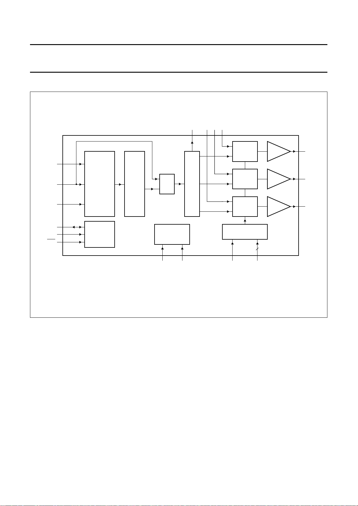
The SAA7167A is a mixed-mode designed IC containing a
video data path, keying control block, analog mixer, and a
C-bus
SAA7167A
voltage output amplifier, capable of converting digital video
data to analog RGB video, and then mixing video and
external analog RGB inputs.
The video data path contains a data re-formatter,
YUV-to-RGB colour space matrix as well as triple DACs for
video data processing. An analog mixer performs
multiplexing between DAC outputs of the video path and
external analog RGB inputs.
The final analog outputs are buffered with built-in voltage
output amplifiers to provide the direct driving capability for
a 150 Ω load. Figure 1 shows the overall block diagram.
2
The operation of SAA7167 is controlled via the I
C-bus.
QUICK REFERENCE DATA
SYMBOL PARAMETER MIN. MAX. UNIT
V
DDD
V
DDA
T
amb
ORDERING INFORMATION
TYPE
NUMBER
SAA7167A LQFP48 plastic low profile quad flat package; 48 leads; body 7 × 7 × 1.4 mm SOT313-2
digital supply voltage 4.75 5.25 V
analog supply voltage 4.75 5.25 V
operating ambient temperature 0 70 °C
PACKAGE
NAME DESCRIPTION VERSION
1996 Aug 14 2
Page 3
Philips Semiconductors Preliminary specification
YUV-to-RGB Digital-to-Analog
Converter DAC
BLOCK DIAGRAM
handbook, full pagewidth
YUV7 to
YUV0
UV7 to
UV0
HREF
SDA
SCL
RES
38 to
45
46 to 48,
1 to 5
9
22
23
24
RE-
FORMATTER
2
C-BUS
I
CONTROL
YUV
TO
RGB
MATRIX
SAA7167A
C
ref(h)
Bin Gin Rin
2936 31 33
MIXER
8-BIT
MUX
CLOCK
GENERATOR
VCLK PCLK EXTKEY P7 to P0
DAC
(3×)
MIXER
MIXER
KEYING CONTROL
8
13 to 2021106
SAA7167A
OPAMP
OPAMP
OPAMP
32
30
28
MBH532
Rout
Gout
Bout
Fig.1 Block diagram.
1996 Aug 14 3
Page 4

Philips Semiconductors Preliminary specification
YUV-to-RGB Digital-to-Analog
SAA7167A
Converter DAC
PINNING
SYMBOL PIN DESCRIPTION I/O
UV4 1 digital video UV (of YUV format 4:1:1 and 4:2:2) input data, or digital G and R
input data
UV3 2 digital video UV (of YUV format 4:1:1 and 4:2:2) input data, or digital G and R
input data
UV2 3 digital video UV (of YUV format 4:1:1 and 4:2:2) input data, or digital G and R
input data
UV1 4 digital video UV (of YUV format 4:1:1 and 4:2:2) input data, or digital G and R
input data
UV0 5 digital video UV (of YUV format 4:1:1 and 4:2:2) input data, or digital G and R
input data
VCLK 6 video clock input I
V
DDD
V
SSD
HREF 9 horizontal reference input signal I
PCLK 10 pixel clock input I
AP 11 test pins, normally connected to ground I
SP 12 test pins, normally connected to ground I
P7 13 pixel bus input 7 (for keying control) I
P6 14 pixel bus input 6 (for keying control) I
P5 15 pixel bus input 5 (for keying control) I
P4 16 pixel bus input 4 (for keying control) I
P3 17 pixel bus input 3 (for keying control) I
P2 18 pixel bus input 2 (for keying control) I
P1 19 pixel bus input 1 (for keying control) I
P0 20 pixel bus input 0 (for keying control) I
EXTKEY 21 external key signal input I
SDA 22 I
SCL 23 I
RES 24 set to LOW to reset the I2C-bus I
n.c. 25 not connected −
V
SSA2
V
DDA2
Bout 28 analog Blue signal output O
Bin 29 analog Blue signal input I
Gout 30 analog Green signal output O
Gin 31 analog Green signal input I
Rout 32 analog Red signal output O
Rin 33 analog Red signal input I
V
SSA1
V
DDA1
C
ref(h)
7 digital supply voltage I/O
8 digital ground I/O
2
C-bus data line I/O
2
C-bus clock line I
26 analog ground 2 I/O
27 analog supply voltage 2 I/O
34 analog ground 1 I/O
35 analog supply voltage 1 I/O
36 capacitor for reference high voltage output (2.25 V) I/O
I
I
I
I
I
1996 Aug 14 4
Page 5

Philips Semiconductors Preliminary specification
YUV-to-RGB Digital-to-Analog
SAA7167A
Converter DAC
SYMBOL PIN DESCRIPTION I/O
n.c. 37 not connected −
YUV7 38 digital video Y or UV (of YUV format 2:1:1) input data, or digital G and B input data I
YUV6 39 digital video Y or UV (of YUV format 2:1:1) input data, or digital G and B input data I
YUV5 40 digital video Y or UV (of YUV format 2:1:1) input data, or digital G and B input data I
YUV4 41 digital video Y or UV (of YUV format 2:1:1) input data, or digital G and B input data I
YUV3 42 digital video Y or UV (of YUV format 2:1:1) input data, or digital G and B input data I
YUV2 43 digital video Y or UV (of YUV format 2:1:1) input data, or digital G and B input data I
YUV1 44 digital video Y or UV (of YUV format 2:1:1) input data, or digital G and B input data I
YUV0 45 digital video Y or UV (of YUV format 2:1:1) input data, or digital G and B input data I
UV7 46 digital video UV (of YUV format 4:1:1 and 4:2:2) input data, or digital G and R
input data
UV6 47 digital video UV (of YUV format 4:1:1 and 4:2:2) input data, or digital G and R
input data
UV5 48 digital video UV (of YUV format 4:1:1 and 4:2:2) input data, or digital G and R
input data
I
I
I
UV4
UV3
UV2
UV1
UV0
VCLK
V
DDD
V
SSD
HREF
PCLK
index
corner
AP
SP
UV7
UV6
47
14
P6
46
15
P5
YUV0
YUV1
45
44
SAA7167A
16
17
P4
P3
UV5
48
1
2
3
4
5
6
7
8
9
10
11
12
13
P7
YUV2
43
18
P2
YUV3
42
19
P1
YUV4
41
20
P0
YUV5
YUV6
40
39
21
22
SDA
EXTKEY
YUV7
38
23
SCL
n.c.
24 37
RES
36
35
34
33
32
31
30
29
28
27
26
25
MBH531
C
ref(h)
V
DDA1
V
SSA1
Rin
Rout
Gin
Gout
Bin
Bout
V
DDA2
V
SSA2
n.c.
1996 Aug 14 5
Fig.2 Pin configuration.
Page 6

Philips Semiconductors Preliminary specification
YUV-to-RGB Digital-to-Analog
Converter DAC
FUNCTIONAL DESCRIPTION
The SAA7167A contains a video data path, 3 analog
mixers and voltage output amplifiers for the RGB channels
respectively, a keying control block as well as an I2C-bus
control block.
Video data path
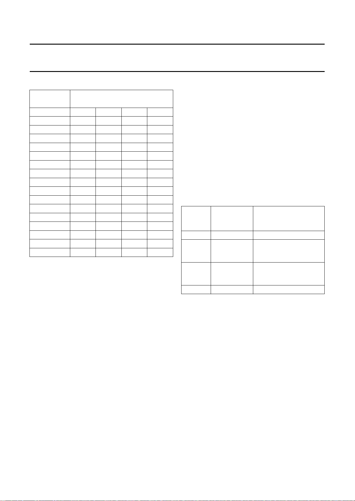
The video data path includes a video data re-formatter, a
YUV-to-RGB colour space conversion matrix, and triple
8-bit DACs.
E-FORMATTER
R
The re-formatter de-multiplexes the different video formats
YUV 4 :1:1, 4:2:2 or 2:1:1 to internal YUV 4 : 4 : 4,
which can then be processed by the RGB matrix. The pixel
byte sequences of those video input formats are shown in
Tables 1 to 4.
Table 1 Pixel byte sequence of 4 :2:2
INPUT
YUV0 (LSB)
YUV1
YUV2
YUV3
YUV4
YUV5
YUV6
YUV7 (MSB)
UV0 (LSB)
UV1
UV2
UV3
UV4
UV5
UV6
UV7 (MSB)
Y data
UV data
PIXEL BYTE SEQUENCE OF
4:2:2
Y0 Y0 Y0 Y0 Y0 Y0
Y1 Y1 Y1 Y1 Y1 Y1
Y2 Y2 Y2 Y2 Y2 Y2
Y3 Y3 Y3 Y3 Y3 Y3
Y4 Y4 Y4 Y4 Y4 Y4
Y5 Y5 Y5 Y5 Y5 Y5
Y6 Y6 Y6 Y6 Y6 Y6
Y7 Y7 Y7 Y7 Y7 Y7
U0 V0 U0 V0 U0 V0
U1 V1 U1 V1 U1 V1
U2 V2 U2 V2 U2 V2
U3 V3 U3 V3 U3 V3
U4 V4 U4 V4 U4 V4
U5 V5 U5 V5 U5 V5
U6 V6 U6 V6 U6 V6
U7 V7 U7 V7 U7 V7
012345
024
SAA7167A
Table 2 Pixel byte sequence of 4:1:1
INPUT PIXEL BYTE SEQUENCE OF 4:1:1
YUV0
YUV1
YUV2
YUV3
YUV4
YUV5
YUV6
YUV7
UV0
UV1
UV2
UV3
UV4
UV5
UV6
UV7
Y data
UV data
Table 3 Pixel byte sequence of 2:1:1
INPUT PIXEL BYTE SEQUENCE OF 2:1:1
YUV0
YUV1
YUV2
YUV3
YUV4
YUV5
YUV6
YUV7
Y data
UV data
Y0 Y0 Y0 Y0 Y0 Y0 Y0 Y0
Y1 Y1 Y1 Y1 Y1 Y1 Y1 Y1
Y2 Y2 Y2 Y2 Y2 Y2 Y2 Y2
Y3 Y3 Y3 Y3 Y3 Y3 Y3 Y3
Y4 Y4 Y4 Y4 Y4 Y4 Y4 Y4
Y5 Y5 Y5 Y5 Y5 Y5 Y5 Y5
Y6 Y6 Y6 Y6 Y6 Y6 Y6 Y6
Y7 Y7 Y7 Y7 Y7 Y7 Y7 Y7
XXXXXXXX
XXXXXXXX
XXXXXXXX
XXXXXXXX
V6 V4 V2 V0 V6 V4 V2 V0
V7 V5 V3 V1 V7 V5 V3 V1
U6 U4 U2 U0 U6 U4 U2 U0
U7 U5 U3 U1 U7 U5 U3 U1
01234567
04
U0 Y0 V0 Y0 U0 Y0 V0 Y0
U1 Y1 V1 Y1 U1 Y1 V1 Y1
U2 Y2 V2 Y2 U2 Y2 V2 Y2
U3 Y3 V3 Y3 U3 Y3 V3 Y3
U4 Y4 V4 Y4 U4 Y4 V4 Y4
U5 Y5 V5 Y5 U5 Y5 V5 Y5
U6 Y6 V6 Y6 U6 Y6 V6 Y6
U7 Y7 V7 Y7 U7 Y7 V7 Y7
X0X2X4X6
0X0X4X4X
1996 Aug 14 6
Page 7
Philips Semiconductors Preliminary specification
YUV-to-RGB Digital-to-Analog
Converter DAC
Table 4 Pixel byte sequence of 5 :6:5
INPUT
UV7
UV6
UV5
UV4
UV3
UV2
UV1
UV0
YUV7
YUV6
YUV5
YUV4
YUV3
YUV2
YUV1
YUV0
RGB data
For RGB 5 :6:5 video inputs, the video data are just
directly bypassed to triple DACs.
The input video data can be selected to either two’s
complement (I
(DRP-bit = 1). The video input format is selected by
I2C-bus bits FMTC1 and FMTC0.
The rising edge of HREF input defines the start of active
video data. When HREF is inactive, the video output will be
blanked.
YUV-
TO-RGB MATRIX
The matrix converts YUV data, in accordance with
CCIR-601, to RGB data with approximately 1.5 LSB
deviation to the theoretical values for 8-bit resolution.
T
RIPLE 8-BIT DACS
Three identical DACs for R, G and B video outputs are
designed with voltage-drive architecture to provide
high-speed operation of up to 66 MHz conversion data
rate. A C
ref(h)
de-coupling capacitor to be connected between the
internal reference voltage source and ground.
PIXEL BYTE SEQUENCE OF RGB
5:6:5
G0 G0 G0 G0
R4 R4 R4 R4
R3 R3 R3 R3
R2 R2 R2 R2
R1 R1 R1 R1
R0 R0 R0 R0
G5 G5 G5 G5
G4 G4 G4 G4
G3 G3 G3 G3
G2 G2 G2 G2
G1 G1 G1 G1
B4 B4 B4 B4
B3 B3 B3 B3
B2 B2 B2 B2
B1 B1 B1 B1
B0 B0 B0 B0
0123
2
C-bus DRP-bit = 0) or binary offset
pin is provided to allow for one external
SAA7167A
Analog mixers and keying control
The analog mixers are controlled to switch between the
outputs from the video DACs and analog RGB inputs by a
keying signal. The analog RGB inputs need to interface
with analog mixers in the way of DC-coupling, also these
RGB inputs are limited to RGB signals without a sync level
pedestal. The keying control can be enabled by setting I2C
bit KEN = 1. Two kinds of keying are possible to generate:
one is external key (from EXTKEY pin when
KMOD2 to KMOD0 are logic 0), and the other is the
internal pixel colour key (when KMOD2 to KMOD0 are not
logic 0) generated by comparing the input pixel data with
the internal I
by KMOD2 to KMOD0 bits, there are 4 ways to compare
the pixel data (see Table 5).
Table 5 KMOD2 to KMOD0
KMOD2
to
KMOD0
1 0 0 8-bit pixel pseudo colour mode
101 2×8-bit pixel high colour mode 1 with
110 2×8-bit pixel high colour mode 2 with
111 3×8-bit pixel true colour mode
Since only one control register KD7 to KD0 provides the
data value for pixel data comparison, when at 2 × 8-bit or
3 × 8-bit pixel input modes, it is presumed that all input
bytes (lower, middle, or higher) of each pixel must be same
as KD7 to KD0 in order to make graphics colour key
active.
The polarity of EXTKEY can be selected with KINV. With
KINV = 0, EXTKEY = HIGH switches analog mixers to
select DAC outputs. Before the internal keying signal
switches the analog multiplexers, it can be further delayed
up to 7 PCLK cycles with the control bits
KDLY2 to KDLY0.
2
C-bus register value KD7 to KD0. Controlled
PIXEL TYPE REMARK
pixels given at both rising
and falling edges of PCLK
pixels given only at rising
edges of PCLK
1996 Aug 14 7
Page 8
Philips Semiconductors Preliminary specification
YUV-to-RGB Digital-to-Analog
SAA7167A
Converter DAC
Voltage output amplifiers
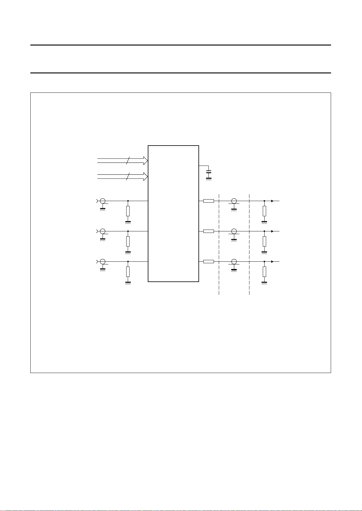
Before the analog input enters the analog mixers, it passes
through voltage output amplifiers. Level shifters are used
internally to provide an offset of 0.2 V and an amplifier gain
of 2 for analog inputs to match with the output levels from
DACs. After buffering with voltage output amplifiers, the
final RGB outputs can drive a 150 Ω load directly (25 Ω
internal resistor, 50 Ω external serial resistor, and 75 Ω
load resistor at monitor side (see Fig.9).
2
I
C-bus control
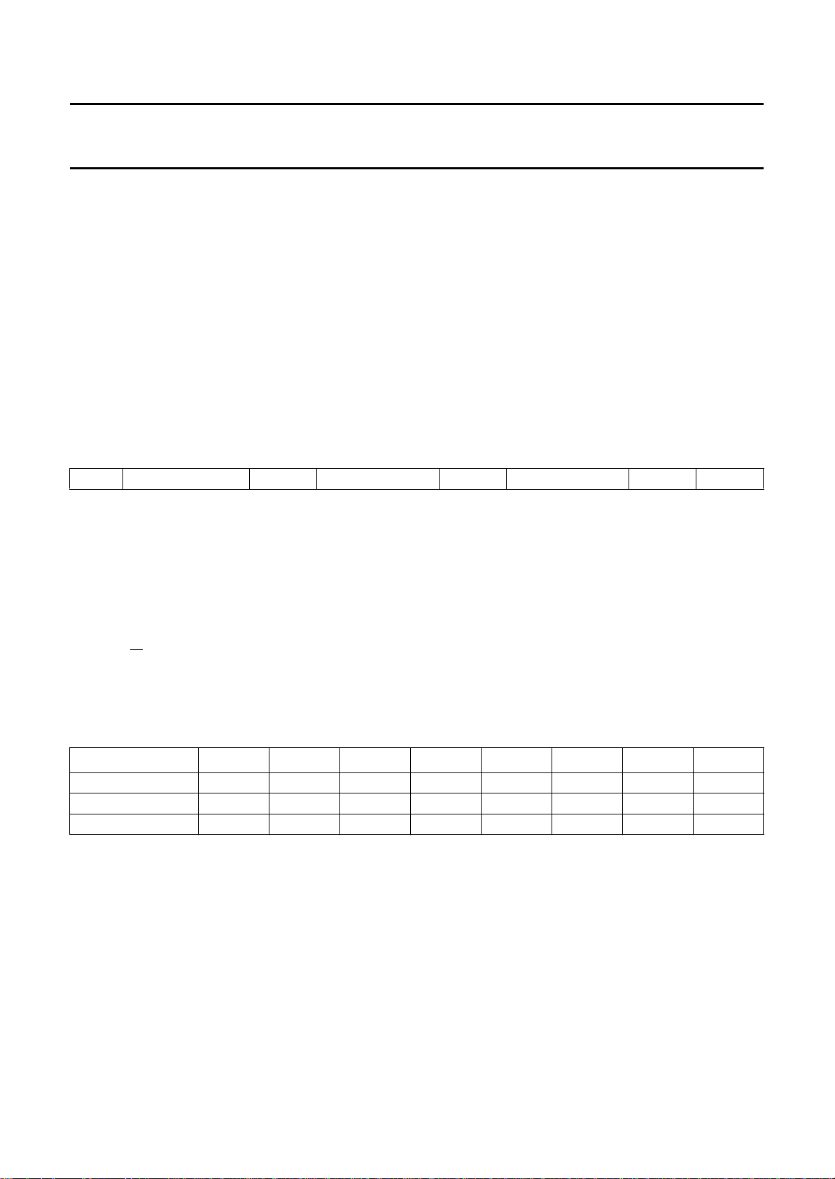
Only one control byte is needed for the SAA7167A.
The I2C-bus format is shown in Table 6.
2
Table 6 I
S slave address A subaddress A data A P
Notes
1. S = START condition.
2. Slave address = 1011 111X; this slave address is identical to the one for the SAA9065.
3. A = acknowledge; generated by the slave.
4. Subaddress = subaddress byte.
5. Data = data byte.
6. P = STOP condition.
7. X = R/
a) X = 0; order to write.
b) X = 1; order to read (not used for SAA7167A).
C-bus format; see notes 1 to 7
W control bit:
The output voltage level of DAC ranges from the lowest
level 0.2 V (zero code) to the highest level 1.82 V (all one
code).
With the digital input YUV video data in accordance with
CCIR-601, the RGB output of 8-bit DAC actually ranges
from the 16th step (black) to the 235th step (white).
Therefore, after the voltage divider with external serial
resistor and monitor load resistor, the output voltage range
to monitor is approximately 0.7 V (peak-to-peak).
Table 7 Control data byte
SUBADDRESS D7 D6 D5 D4 D3 D2 D1 D0
00 KMOD2 KMOD1 KMOD0 DRP KEN KINV FMTC1 FMTC0
01 00000KDLY2KDLY1KDLY0
02 KD7 KD6 KD5 KD4 KD3 KD2 KD1 KD0
1996 Aug 14 8
Page 9
Philips Semiconductors Preliminary specification
YUV-to-RGB Digital-to-Analog
Converter DAC
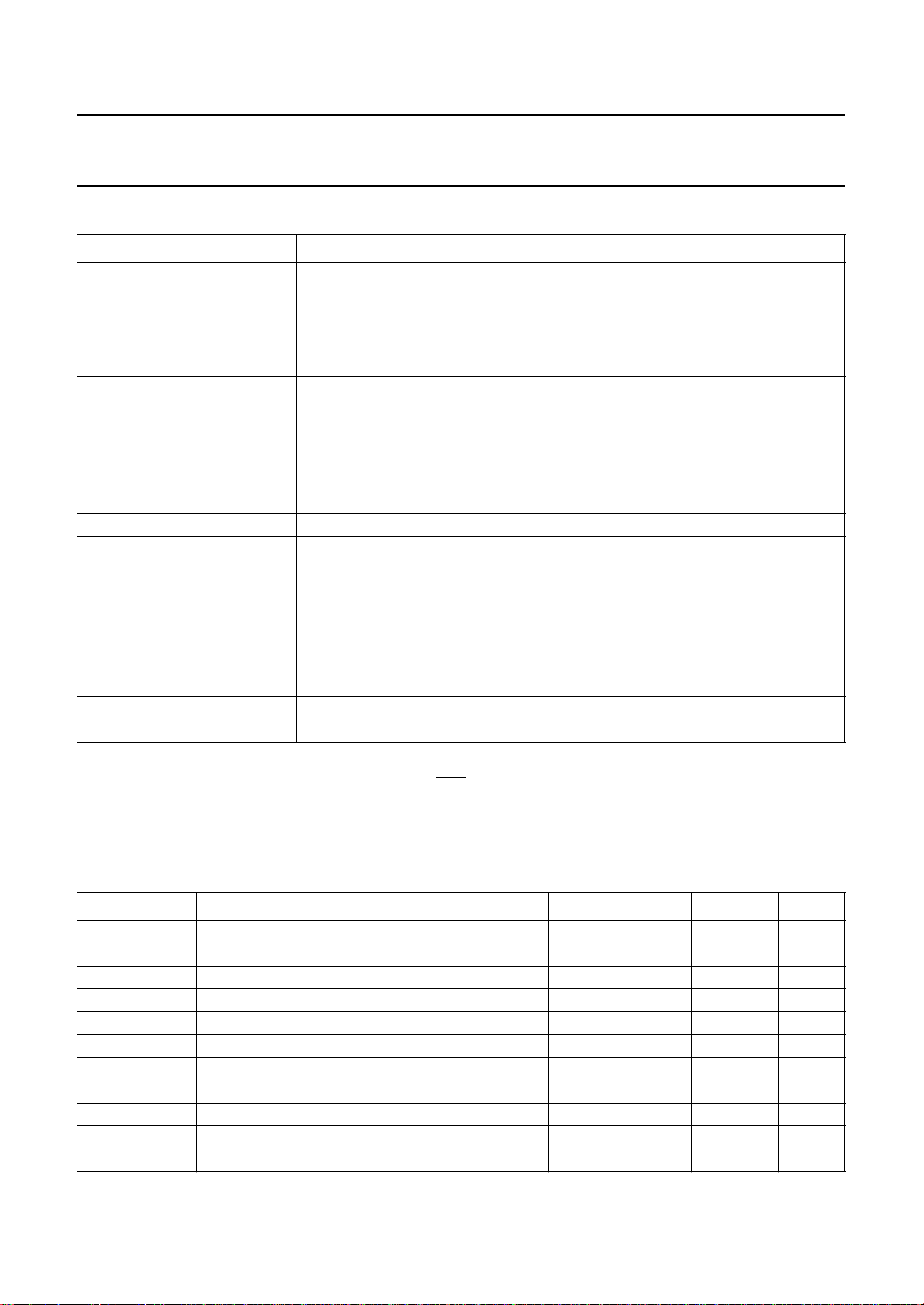
Table 8 Bit functions in data byte; notes 1 and 2
BIT DESCRIPTION
FMTC1 and FMTC0 video format control:
00; YUV 4 :2:2
01; YUV 4 :1:1
10; YUV 2 : 1 : 1/CCIR-656
11; RGB 5 :6:5
KINV key polarity:
KINV = 0: EXTKEY = HIGH for analog mixer to select DAC outputs
KINV = 1: EXTKEY = HIGH for analog mixer to select analog RGB inputs
KEN key enable:
0 = disable
1 = enable
DRP UV input data code: 0 = two’s complement; 1 = binary offset
KMOD2 to KMOD0 keying mode:
000; external key
100; 8-bit pixel colour key
101; 2 × 8-bit pixel colour key (with two-edge clock latching for pixel input)
110; 2 × 8-bit pixel colour key (with one-edge clock latching for pixel input)
111; 3 × 8-bit pixel colour key (with one-edge clock latching for pixel input)
all other combinations are reserved
KDLY2 to KDLY0 added keying delay cycles (from 0 to 7 PCLK)
KD7 to KD0 the data value compared for 8, 16 or 24-bit pixel colour key
SAA7167A
Notes
1. All I
2
C-bus control bits are initialized to logic 0 after RES is activated.
2. PCLK should be active in any event to allow for correct operation of I2C-bus programming.
DC CHARACTERISTICS
T
= 0 to 70 °C.
amb
SYMBOL PARAMETER MIN. TYP. MAX. UNIT
V
DDD
V
DDA
I
DDtot
V
IH
V
IL
V
IH
V
IL
V
in
V
out
digital supply voltage 4.75 5.0 5.25 V
analog supply voltage 4.75 5.0 5.25 V
total supply current (f
HIGH level input voltage (pin SDA) 3 − V
= 66 MHz) − 105 − mA
clk
+ 0.5 V
DDD
LOW level input voltage (pin SDA) −0.5 − +1.5 V
HIGH level digital input voltage 2 −− V
LOW level digital input voltage −−0.8 V
full-scale analog RGB inputs − 0.7 − V
full scale analog RGB outputs (for 150 Ω load) − 1.4 − V
DNL differential non-linearity error of video output −−1 LSB
INL integral non-linearity error of video output −−1 LSB
1996 Aug 14 9
Page 10
Philips Semiconductors Preliminary specification
YUV-to-RGB Digital-to-Analog
SAA7167A
Converter DAC
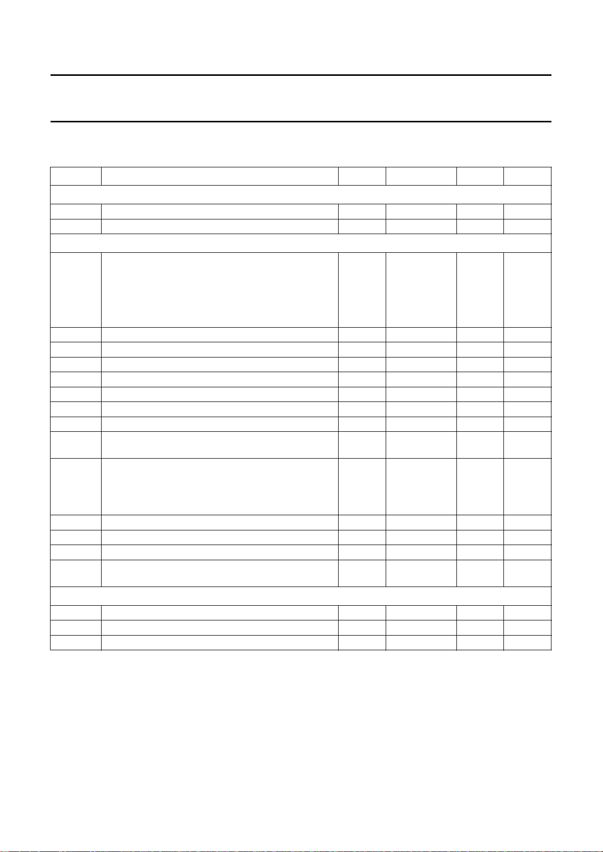
AC CHARACTERISTICS
T
= 0 to 70 °C.
amb
SYMBOL PARAMETER MIN. TYP. MAX. UNIT
VCLK
f
clk
δ duty factor of VCLK 40 50 60 %
PCLK
f
clk
δ duty factor of PCLK 40 50 60 %
t
su1
t
h1
t
su2
t
h2
t
su3
t
h3
t
sw
T
group
t
r
t
f
t
s
t
PD
video clock rate −− 66 MHz
pixel clock rate
8-bit pixel colour key; see Fig.4 −− 77.5 MHz
2 × 8-bit pixel colour key; mode 1; see Fig.5 −− 50 MHz
2 × 8-bit pixel colour key; mode 2; see Fig.6 −− 80 MHz
3 × 8-bit pixel colour key; see Fig.7 −− 77.5 MHz
digital input set-up time to VCLK rising edge 3 −−ns
digital input hold time to VCLK rising edge 2 −−ns
digital input set-up time to PCLK rising edge 0 −−ns
digital input hold time to PCLK rising edge 4.2 −−ns
digital input set-up time to PCLK falling edge −1 −−ns
digital input hold time to PCLK falling edge 6 −−ns
switching time between video DAC/analog inputs;
−− 15 ns
note 1
overall group delay from digital video inputs to analog
outputs (see Fig.8):
YUV video input mode − 20T
RGB video input mode − 12T
VCLK+tPD
VCLK+tPD
− ns
− ns
DAC analog output rise time (see Fig.8); note 2 − 3.5 − ns
DAC analog output fall time (see Fig.8); note 2 − 3.5 − ns
DAC analog output settling time (see Fig.8); note 3 − 16.5 − ns
DAC analog output propagation delay (see Fig.8);
− 20 − ns
note 4
Analog outputs from analog inputs
G
v
voltage gain − 2.0 −
B bandwidth (−3 dB) 160 −−MHz
SR slew rate 100 110 − V/µs
Notes
1. Switching time measured from the 50% point of the EXTKEY transition edge to the 50% point of the selected analog
output transition.
2. DAC output rise/fall time measured between the 10% and 90% points of full scale transition.
3. DAC settling time measured from the 50% point of full-scale transition to the output remaining within ±1 LSB.
4. DAC analog output propagation delay measured from the 50% point of the rising edge of VCLK to the 50% point of
full-scale transition.
1996 Aug 14 10
Page 11
Philips Semiconductors Preliminary specification
YUV-to-RGB Digital-to-Analog
Converter DAC
handbook, full pagewidth
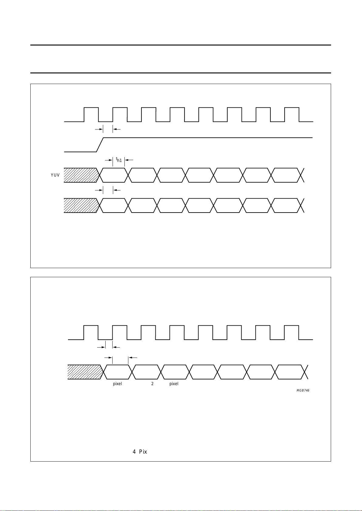
VCLK
t
su1
HREF
t
h1
YUV
t
su1
UV
SAA7167A
MGB745
handbook, full pagewidth
PCLK
P7 to P0
Fig.3 Video data input timing.
t
su2
t
h2
pixel 1 pixel 2 pixel 3 pixel 4 pixel 5 pixel 6 pixel 7
MGB746
1996 Aug 14 11
Fig.4 Pixel data timing; 8-bit pixel colour key.
Page 12
Philips Semiconductors Preliminary specification
YUV-to-RGB Digital-to-Analog
Converter DAC
handbook, full pagewidth
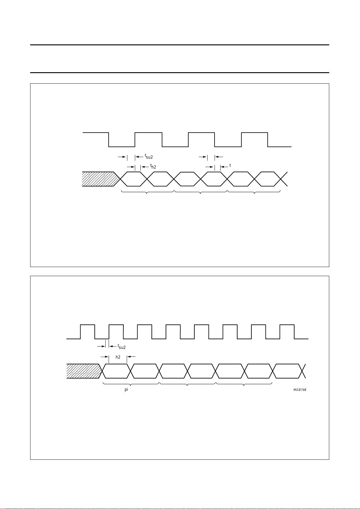
PCLK
P7 to P0
t
su2
t
h2
pixel 1 pixel 2 pixel 3
t
su3
t
h3
SAA7167A
MGB747
handbook, full pagewidth
PCLK
P7 to P0
Fig.5 Pixel data input timing; 2 × 8-bit pixel colour key; mode 1.
t
su2
t
h2
pixel 1
pixel 2 pixel 3
MGB748
1996 Aug 14 12
Fig.6 Pixel data input timing; 2 × 8-bit pixel colour key; mode 2.
Page 13
Philips Semiconductors Preliminary specification
YUV-to-RGB Digital-to-Analog
Converter DAC
handbook, full pagewidth
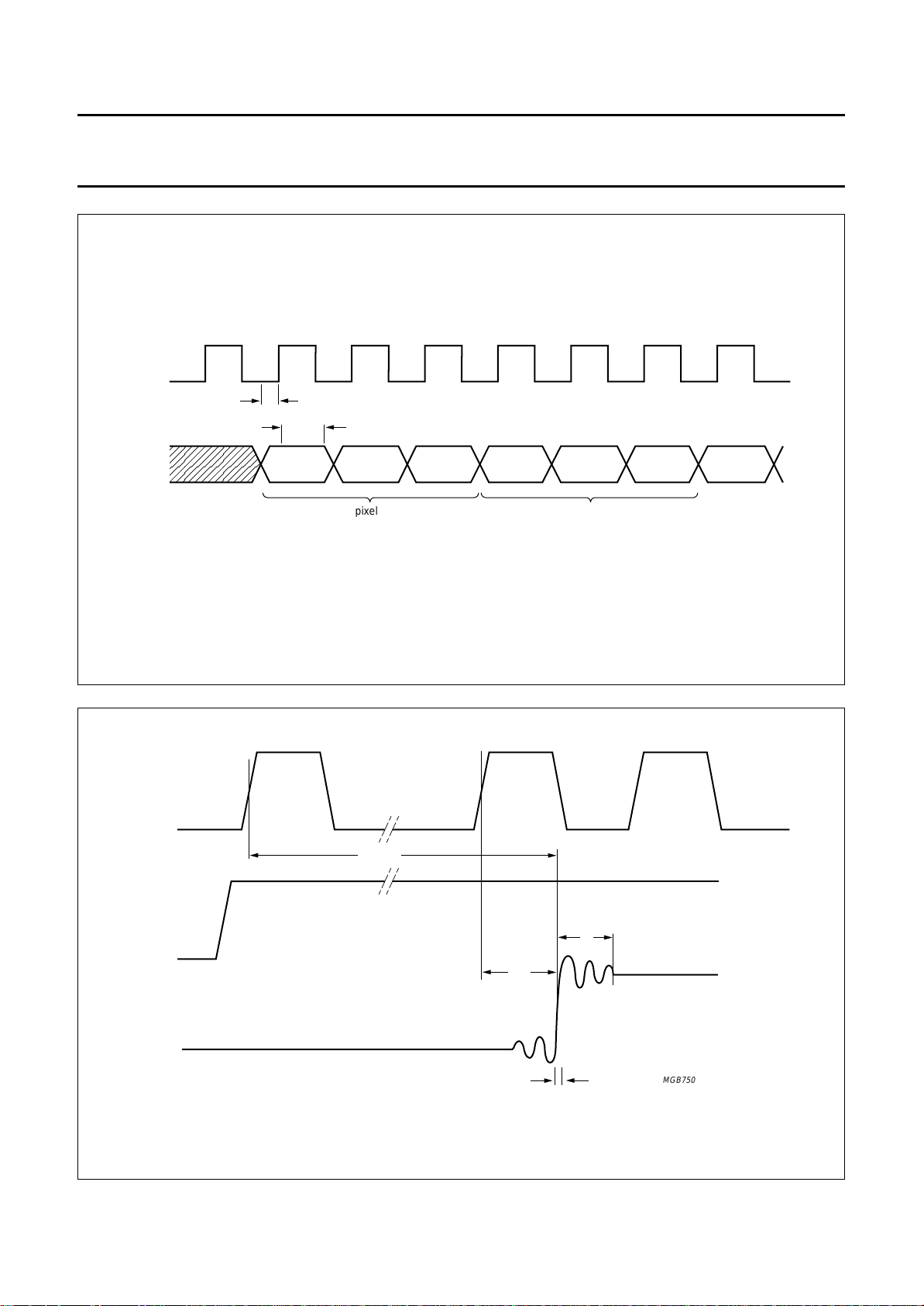
PCLK
P7 to P0
t
su2
t
h2
pixel 1
pixel 2
SAA7167A
MGB749
handbook, full pagewidth
VCLK
YUV and UV
Rout, Bout and Gout
Fig.7 Pixel data input timing; 3 × 8-bit pixel colour key.
T
group
(full-scale transition)
t
s
t
PD
tr; t
f
MGB750
1996 Aug 14 13
Fig.8 DAC output timing.
Page 14
Philips Semiconductors Preliminary specification
YUV-to-RGB Digital-to-Analog
Converter DAC
APPLICATION INFORMATION
handbook, full pagewidth
digital YUV video data inputs
8
YUV7 to YUV0
8
UV7 to UV0
analog inputs from VGA
75 Ω 75 Ω
75 Ω
Rin
Gin
38 to 45
46 to 48,
1 to 5
33
31
SAA7167A
36
32
30
C
ref(h)
0.1 µF
to PC monitor
47 Ω
Rout
47 Ω
Gout
SAA7167A
75 Ω
47 Ω
28
Bout
MBH533
cable monitor side
75 Ω
Bin
29
Fig.9 Typical application diagram for analog circuits.
75 Ω
1996 Aug 14 14
Page 15
Philips Semiconductors Preliminary specification
YUV-to-RGB Digital-to-Analog
Converter DAC
PACKAGE OUTLINE
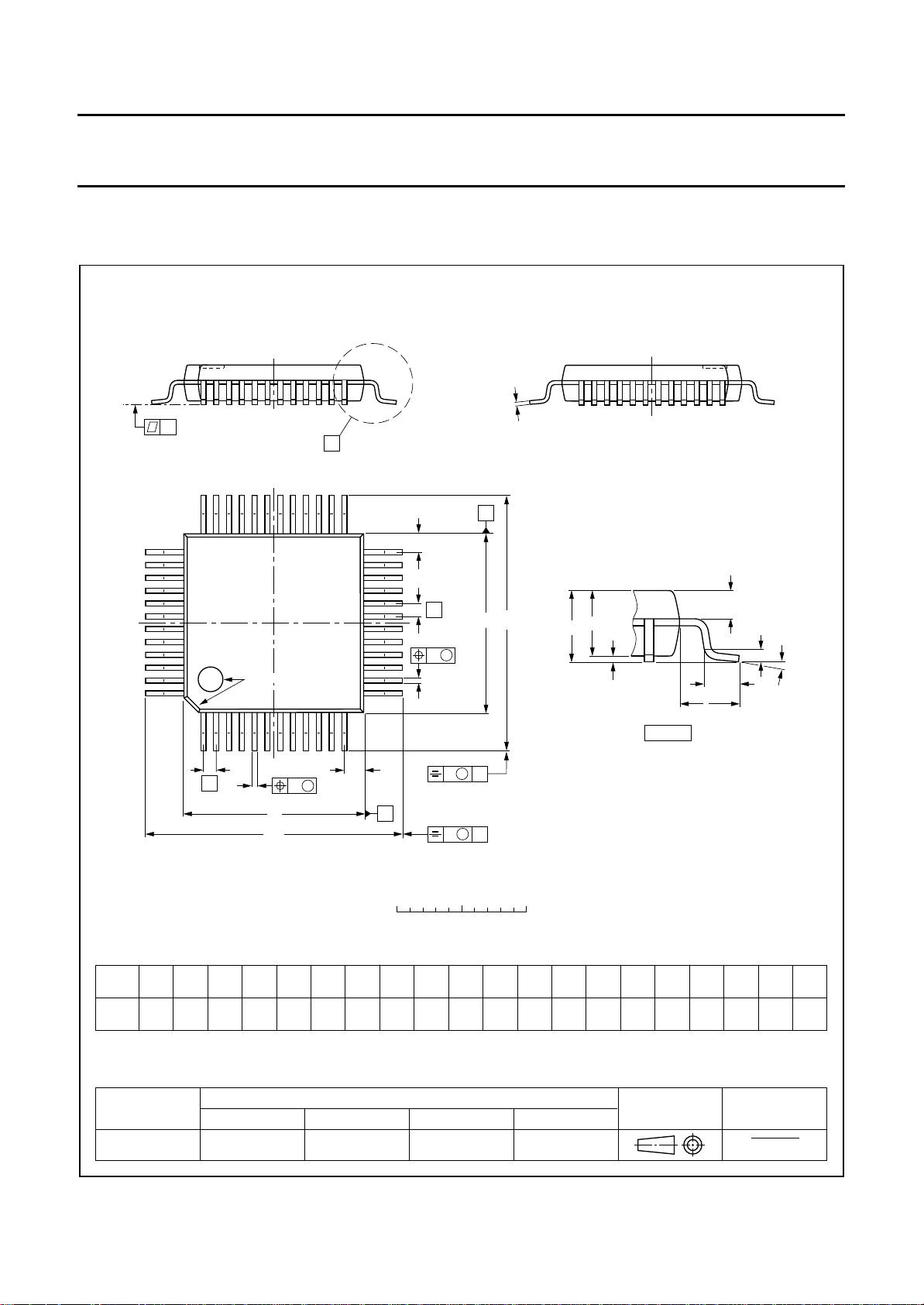
LQFP48: plastic low profile quad flat package; 48 leads; body 7 x 7 x 1.4 mm
c
y
X
36
37
25
Z
24
E
A
SAA7167A
SOT313-2
e
w M
pin 1 index
48
1
e
DIMENSIONS (mm are the original dimensions)
mm
A
A1A2A3b
max.
0.20
1.60
0.05
1.45
1.35
UNIT
Note
1. Plastic or metal protrusions of 0.25 mm maximum per side are not included.
b
p
0.25
w M
D
H
D
p
0.27
0.17
12
Z
D
(1) (1)(1)
cE
D
0.18
7.1
0.12
6.9
b
p
13
v M
B
v M
0 2.5 5 mm
scale
(1)
eH
H
7.1
6.9
0.5
9.15
8.85
D
E
A
B
9.15
8.85
H
E
LLpQZywv θ
E
0.75
0.45
A
2
A
A
1
detail X
0.69
0.59
0.12 0.10.21.0
Q
(A )
3
θ
L
p
L
Z
E
D
0.95
0.55
0.95
0.55
o
7
o
0
OUTLINE
VERSION
SOT313-2
1996 Aug 14 15
REFERENCES
IEC JEDEC EIAJ
EUROPEAN
PROJECTION
ISSUE DATE
93-06-15
94-12-19
Page 16

Philips Semiconductors Preliminary specification
YUV-to-RGB Digital-to-Analog
Converter DAC
SOLDERING
Introduction
There is no soldering method that is ideal for all IC
packages. Wave soldering is often preferred when
through-hole and surface mounted components are mixed
on one printed-circuit board. However, wave soldering is
not always suitable for surface mounted ICs, or for
printed-circuits with high population densities. In these
situations reflow soldering is often used.
This text gives a very brief insight to a complex technology.
A more in-depth account of soldering ICs can be found in
our
“IC Package Databook”
Reflow soldering
Reflow soldering techniques are suitable for all LQFP
packages.
Reflow soldering requires solder paste (a suspension of
fine solder particles, flux and binding agent) to be applied
to the printed-circuit board by screen printing, stencilling or
pressure-syringe dispensing before package placement.
Several techniques exist for reflowing; for example,
thermal conduction by heated belt. Dwell times vary
between 50 and 300 seconds depending on heating
method. Typical reflow temperatures range from
215 to 250 °C.
Preheating is necessary to dry the paste and evaporate
the binding agent. Preheating duration: 45 minutes at
45 °C.
Wave soldering
Wave soldering is not recommended for LQFP packages.
This is because of the likelihood of solder bridging due to
closely-spaced leads and the possibility of incomplete
solder penetration in multi-lead devices.
(order code 9398 652 90011).
SAA7167A
If wave soldering cannot be avoided, the following
conditions must be observed:
• A double-wave (a turbulent wave with high upward
pressure followed by a smooth laminar wave)
soldering technique should be used.
• The footprint must be at an angle of 45° to the board
direction and must incorporate solder thieves
downstream and at the side corners.
Even with these conditions, do not consider wave
soldering LQFP packages LQFP48 (SOT313-2),
LQFP64 (SOT314-2) or LQFP80 (SOT315-1).
During placement and before soldering, the package must
be fixed with a droplet of adhesive. The adhesive can be
applied by screen printing, pin transfer or syringe
dispensing. The package can be soldered after the
adhesive is cured.
Maximum permissible solder temperature is 260 °C, and
maximum duration of package immersion in solder is
10 seconds, if cooled to less than 150 °C within
6 seconds. Typical dwell time is 4 seconds at 250 °C.
A mildly-activated flux will eliminate the need for removal
of corrosive residues in most applications.
Repairing soldered joints
Fix the component by first soldering two diagonallyopposite end leads. Use only a low voltage soldering iron
(less than 24 V) applied to the flat part of the lead. Contact
time must be limited to 10 seconds at up to 300 °C. When
using a dedicated tool, all other leads can be soldered in
one operation within 2 to 5 seconds between
270 and 320 °C.
1996 Aug 14 16
Page 17
Philips Semiconductors Preliminary specification
YUV-to-RGB Digital-to-Analog
SAA7167A
Converter DAC
DEFINITIONS
Data sheet status
Objective specification This data sheet contains target or goal specifications for product development.
Preliminary specification This data sheet contains preliminary data; supplementary data may be published later.
Product specification This data sheet contains final product specifications.
Limiting values
Limiting values given are in accordance with the Absolute Maximum Rating System (IEC 134). Stress above one or
more of the limiting values may cause permanent damage to the device. These are stress ratings only and operation
of the device at these or at any other conditions above those given in the Characteristics sections of the specification
is not implied. Exposure to limiting values for extended periods may affect device reliability.
Application information
Where application information is given, it is advisory and does not form part of the specification.
LIFE SUPPORT APPLICATIONS
These products are not designed for use in life support appliances, devices, or systems where malfunction of these
products can reasonably be expected to result in personal injury. Philips customers using or selling these products for
use in such applications do so at their own risk and agree to fully indemnify Philips for any damages resulting from such
improper use or sale.
PURCHASE OF PHILIPS I
Purchase of Philips I
components in the I2C system provided the system conforms to the I2C specification defined by
Philips. This specification can be ordered using the code 9398 393 40011.
2
C COMPONENTS
2
C components conveys a license under the Philips’ I2C patent to use the
1996 Aug 14 17
 Loading...