

Page 1

INTEGRATED CIRCUITS
DATA SH EET
SAA7151B
Digital multistandard colour
decoder with SCART interface
(DMSD2-SCART)
Product specification
File under Integrated Circuits, IC02
April 1993
Page 2

Philips Semiconductors Product specification
Digital multistandard colour decoder
with SCART interface (DMSD2-SCART)
FEATURES
• 8-bit performance on chip for luminance and
chrominance signal processing for PAL, NTSC and
SECAM standards
• Separate 8-bit luminance and 8-bit chrominance input
signals from Y/C, CVBS, S-Video (S-VHS or Hi8)
sources
• SCART signal insertion by means of RGB/YUV
convertion; fast switch handling
• Horizontal and vertical sync detection for all standards
• Real time control output RTCO
• Fast sync recovery of vertical blanking for VCR signals
(bottom flutter compensation)
• Controls via the I2C-bus
• User programmable aperture correction (horizontal
peaking)
• Cross-colour reduction by chrominance comb-filtering
(NTSC) or by special cross-colour cancellation
(SECAM)
• 8-bit quantization of output signals in 4:1:1 or 4:2:2
formats
• 720 active samples per line
SAA7151B
• The YUV bus supports a data rate of 13.5 MHz
(CCIR 601).
– (864 × f
– (858 × fH) for 60 Hz
• Compatible with memory-based features (line-locked
clock)
• One 24.576 MHz crystal oscillator for all standards
GENERAL DESCRIPTION
The SAA7151B is a digital multistandard colour-decoder
having two 8-bit input channels, one for CVBS or Y, the
other for chrominance or time-multiplexed
colour-difference signals.
) for 50 Hz
H
QUICK REFERENCE DATA
SYMBOL PARAMETER MIN. TYP. MAX. UNIT
V
DD
I
DD
V
I
V
O
T
amb
supply voltage (pins 5, 18, 28, 37 and 52) 4.5 5 5.5 V
total supply current (pins 5, 18, 28, 37 and 52) − 100 250 mA
input levels TTL-compatible
output levels TTL-compatible
operating ambient temperature 0 − 70 °C
ORDERING INFORMATION
EXTENDED TYPE
NUMBER
PINS PIN POSITION MATERIAL CODE
PACKAGE
SAA7151B 68 mini-pack PLCC plastic SOT188
Note
1. SOT188-2; 1996 December 16.
(1)
April 1993 2
Page 3
Philips Semiconductors Product specification
Digital multistandard colour decoder with
SCART interface (DMSD2-SCART)
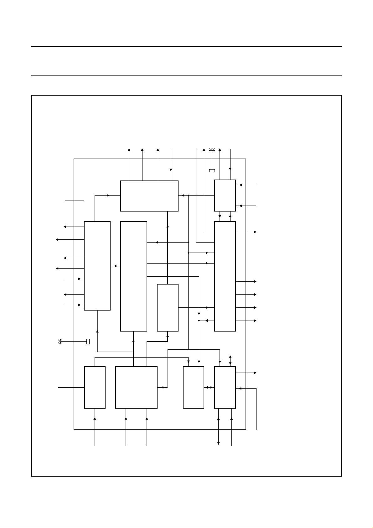
BLOCK DIAGRAM
FEIN
HREF
UV output
(UV7 to UV0)
Y output
(Y7 to Y0)
42
64
53, 54
55 to 62
45 to 50,
1, 2
test pins
GPSW2SYIS
OUTPUT
INTERFACE
DDA
LFCO
V
+5 V
373635
SSA
V
33
XTAL
CLOCK
XTALI
34
SAA7151B
MEH292
39 4 27
ll pagewidth
GPSW1MUXC
CPI
FSO
SCART
FSI
+5 V
44 65 32 24 25
68 66
SS4
to V
SS1
V
DD4
to V
DD1
V
5, 18, 28, 52 19, 38, 51, 67
FAST SWITCH INSERTION
COMPONENT PROCESSING;
SCART INTERFACE CONTROL;
CHROMINANCE PROCESSOR
SAA7151A
14 to 17
20 to 23
CVBS7
CVBS0 to
INPUT
INTERFACE
6 to 13
CUV7
CUV0 to
RESET
POWER-ON
3
RESN
LUMINANCE
PROCESSOR
clock
status
STATUS
REGISTER
SYNCHRONIZATION
C-BUS
2
I
CONTROL
41
40
SCL
SDA
HSY VS HS ODD CREF LL27
Fig.1 Block diagram (application circuits see Figs 17, 18 and 19).
GPSW0 HCL
43 63 26 29 30 31
IICSA
April 1993 3
Page 4

Philips Semiconductors Product specification
Digital multistandard colour decoder with
SAA7151B
SCART interface (DMSD2-SCART)
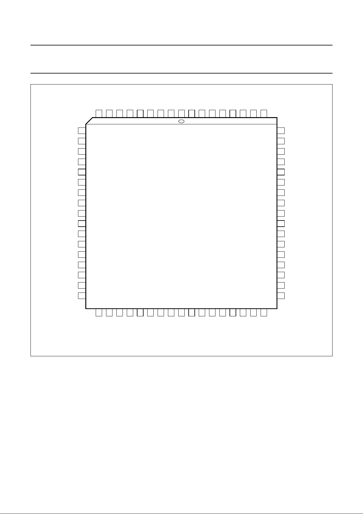
PINNING
SYMBOL PIN DESCRIPTION
SP 1 connected to ground (shift pin for testing)
AP 2 connected to ground (action pin for testing)
RESN 3 reset, active-LOW
CREF 4 clock reference, sync from external to ensure in-phase signals on the Y-, CUV- and YUV-bus
V
DD1
CUV0 6
CUV1 7
CUV2 8
CUV3 9
CUV4 10
CUV5 11
CUV6 12
CUV7 13
CVBS0 14
CVBS1 15
CVBS2 16
CVBS3 17
V
DD2
V
SS1
CVBS4 20
CVBS5 21
CVBS6 22
CVBS7 23
GPSW1 24 status bit output FSST0 or port 1 output for general purpose (programmable by subaddress 0C)
GPSW2 25 status bit output FSST1 or port 2 output for general purpose (programmable by subaddress 0C)
HCL 26 black level clamp pulse output (begin and stop programmable), e.g. for TDA8708A (ADC)
LL27 27 line-locked system clock input signal (27 MHz)
V
DD3
HSY 29 hor. sync pulse reference output (begin and stop programmable), e.g. for gain adj.TDA8708A
VS 30 vertical sync output signal (Fig.11)
HS 31 horizontal sync output signal (Fig.16; start point programmable)
RTCO 32 real time control output; serial increments of HPLL and FSCPLL and status PAL or SECAM
XTAL 33 24.576 MHz clock output (open-circuit for use with external oscillator)
XTALI 34 24.576 MHz connection for crystal or external oscillator (TTL compatible squarewave)
V
SSA
LFCO 36 line frequency control output signal, multiple of horizontal frequency (nominal 6.75 MHz)
V
DDA
V
SS2
5 +5 V supply input 1
chrominance input data bits CUV7 to CUV0 (digitized chrominance signals in two’s complement
format from a S-Video source (S-VHS, Hi8) or time-multiplexed colour-difference signals from a
YUV(RGB) source or both in combination)
CVBS lower input data bits CVBS3 to CVBS0
(CVBS with luminance, chrominance and all sync information in two’s complement format)
18 +5 V supply input 2
19 ground 1 (0 V)
CVBS upper input data bits CVBS7 to CVBS4
(CVBS with luminance, chrominance and all sync information in two’s complement format)
28 +5 V supply input 3
(ADC)
sequence (Fig.10)
35 analog ground
37 +5 V supply input for analog part
38 ground 2 (0 V)
April 1993 4
Page 5

Philips Semiconductors Product specification
Digital multistandard colour decoder with
SAA7151B
SCART interface (DMSD2-SCART)
SYMBOL PIN DESCRIPTION
ODD 39 odd/even field identification output (odd = HIGH)
SDA 40 I
SCL 41 I
HREF 42 horizontal reference for YUV data outputs (for active line 720Y samples long)
IICSA 43 set module address input of I
CPI 44 clamping pulse input (digital clamping of external UV signals)
Y7 45
Y6 46
Y5 47
Y4 48
Y3 49
Y2 50
V
SS3
V
DD4
Y1 53
Y0 54
UV7 55
UV6 56
UV5 57
UV4 58
UV3 59
UV2 60
UV1 61
UV0 62
GPSW0 63 port output for general purpose (programmable by subaddress 0D)
FEIN 64 fast enable input (active-LOW to control fast switching due to YUV data; HIGH = YUV high-Z
MUXC 65 multiplexer control output; source select signal for external ADC (UV signal multiplexing)
FSO 66 fast switch and sync insertion output; gated FS signal from FSI or sync insertion pulse in full screen
V
SS4
FSI 68 fast switch input signal fed from SCART/peri-TV connector (indicates fast insertion of RGB signals)
2
C-bus data line
2
C-bus clock line
Y signal output bits Y7 to Y2 (luminance), part of the digital YUV-bus
51 ground 3 (0 V)
52 +5 V supply input 4
Y signal output bits Y1 to Y0 (luminance), part of the digital YUV-bus
UV signal output bits UV7 to UV0, part of the digital YUV-bus
RGB mode
67 ground 4 (0 V)
2
C-bus (LOW = 1000 101X; HIGH = 1000 111X)
April 1993 5
Page 6
Philips Semiconductors Product specification
Digital multistandard colour decoder with
SCART interface (DMSD2-SCART)
handbook, full pagewidth
CUV0
6
DD1
V
5
CREF
RESNAPSP
4
3
2
SAA7151A
SAA7151B
CUV4
CUV5
CUV6
CUV7
CVBS0
CVBS1
CVBS2
CVBS3
V
DD2
V
SS1
CVBS4
CVBS5
CVBS6
CVBS7
GPSW1
GPSW2
HCL
CUV3
CUV2
CUV1
9
8
7
10
11
12
13
14
15
16
17
18
19
20
21
22
23
24
25
26
SAA7151B
SS4
FSI
V
FSO
MUXC
FEIN
GPSW0
UV0
UV1
1
68
67
66
65
64
63
62
61
60
UV2
59
UV3
58
UV4
57
UV5
56
UV6
55
UV7
54
Y0
53
Y1
52
V
DD4
51
V
SS3
Y2
50
49
Y3
48
Y4
47
Y5
46
Y6
45
Y7
44
CPI
27
28
29
30
31
32
33
34
VS
LL27
DD3
V
HSY
HS
SYIS
XTAL
XTALI
Fig.2 Pin configuration.
FUNCTIONAL DESCRIPTION
System configuration
The SAA7151B system processes digital TV signals with
line-locked clock in PAL, SECAM and NTSC standards
(CVBS or S-Video) as well as RGB signals coming from a
SCART/peri-TV connector. The different source signals
are switched, if necessary matrixed and converted (Fig.3
and Table 1).
8-bit CVBS data (digitized composite video) and 8-bit UV
data (digitized chrominance and /or time-multiplexed
colour-difference signals) are fed to the SAA7151B. The
data rate is 27 MHz.
April 1993 6
35
36
37
38
39
40
41
42
43
SSA
V
LFCO
DDA
V
SS2
V
ODD
SDA
SCL
HREF
MEH293
IICSA
Chrominance processing
The 8-bit chrominance input signal (signal “C” out of CVBS
or Y/C in Fig.4) is fed via the input interface to a bandpass
filter for eliminating the DC component, then to the
quadrature demodulator. Subcarrier signals from the local
oscillator (DTO1) with 90 degree phase shift are applied to
its multiplier inputs. The frequency depends on set TV
standard.
Page 7

Philips Semiconductors Product specification
Digital multistandard colour decoder with
SCART interface (DMSD2-SCART)
handbook, full pagewidth
C
TDA8446
VIDEO
SWITCH AND
MATRIX
SW1
SW2
SCART
CVBS
Y/C
R
G
B
sync
(PERI-TV)
FS
C
Y
2
I C-bus
(select)
TDA8540
VIDEO
SWITCH
CVBS/Y
sync
chroma
CVBS/Y/sync
BP
C
R
G
B
sync
CPI
HCL
FS
*
FSO
U
CSO
CPO
+
V2
U/V
HCT4053
MULTIPLEXER
LP
LP
V
GPSW1
LP
Y
V0
AO
ADI
TDA8709A
8-bit ADC
and multiplexer
(CHROMINANCE)
S0
S1
FE
CLS
CLP
+5 V
from SCART interface SAA7151B
AO
TDA8708A
ADI
8-bit ADC
(LUMINANCE)
GA
GB
SAA7151B
CUV(7-0)
DO(7-0)
CLK
MUXC
clamping
CPI
FSI
CVBS(7-0)
DO(7-0)
CLK
to and from SAA7151B
* fast switching of Y signal for insertion
(UV are switched inside SAA7151B)
Fig.3 System configuration, RGB fast switch interface included (SCART).
The multipliers operate as a quadrature demodulator for all
PAL and NTSC signals; it operates as a frequency
down-mixer for SECAM signals.
The two multiplier output signals are converted to a serial
UV data stream and applied to two low-pass filter stages,
then to a gain controlled amplifier. A final multiplexed
low-pass filter achieves, together with the preceding
stages, the required bandwidth performance. The from
PAL and NTSC originated signals are applied to a
comb-filter. The signals, originated from SECAM, are fed
through a cloche filter (0 Hz centre frequency), a phase
demodulator and a differentiator to obtain
frequency-demodulated colour-difference signals.
The SECAM signals are fed after de-emphasis to a
cross-over switch, to provide the both serial-transmitted
colour-difference signals. These signals are finally fed via
GPSW2
GPSW1
MEH305-3
the fast switch to the output formatter stages and to the
output interface.
Chrominance signals are output in parallel (4:2:2) on the
YUV-bus. The data rate of Y signal (pixel rate) is
13.5 MHz. UV signals have a data rate of 13.5 MHz/2 for
the 4:2.2 format (Table 2) respectively 13.5 MHz/4 for the
4:1.1 format (Table 3).
Component processing and SCART interface control
The 8-bit multiplexed colour-difference input signal (signal
CUV, Fig.1, out of matrixed RGB in Fig.3) is fed via the
input interface to a chrominance stop filter (UV signal only
can pass through; Figures 22 to 24). Here it is clamped
and fed to the offset compensation which can be enabled
or disabled via the I
2
C-bus.
April 1993 7
Page 8
Philips Semiconductors Product specification
Digital multistandard colour decoder with
SCART interface (DMSD2-SCART)
For matrixed RGB signals - the full screen SCART mode
and the fast insertion mode (blanking/switching) are
selectable. The chrominance stop filter is automatically
bypassed in full screen SCART mode.
Full screen RGB mode (SCART):
The CUV digital input signal (7-0) consists of
time-multiplexed samples for U and V. An offset correction
for both signals is applied to correct external clamping
Table 1 SCART interface control (Fig.3)
MODE CONNECTION chroma
output of
FSO GPSW 2 GPSW 1 MUXC
RGB
only
Y/C or
CVBS
only
Fast
switch00
RGB
only
Fast
switch11
0
0
0
0
0
0
1
1
1
1
1
1
0
0
0
0
1
1
1
1
0
0
0
0
1
1
1
1
0
0
1
1
0
0
1
1
0
0
1
1
0
0
1
1
TDA8446
to TDA8709A
0
high-Z VIN2 U/V sync (RGB) sync (RGB)
1
0
C VIN1 C Y (Y/C) or CVBS
1
0
C VIN2
1
0
1
0
high-Z VIN2 U/V Y (RGB) sync (RGB)
1
0
1
0
C VIN2
1
0
1
SAA7151B
errors. An internal timing correction compensates for slight
differences in timing during sampling. The U and V signals
are delay-compensated and fed to the output formatter.
The format 4:2:2 or 4:1:1 is generated by a switchable
filter.
The control signals for the front end (Figures 3 and 20)
MUXC, status bits FSST1, FSST0 (outputs GPSW2,
GPSW1) and FSO are generated by the SAA7151B.
TDA8709A
selected
input
CUV
(7-0)
0.5(C+U)/
0.5(C+V)
0.5(C+U)/
0.5(C+V)
luminance
fast switch
TDA8446
Y (Y/C) or CVBS
not used
not used
Y (RGB)
not used
input
selector (via
2
I
C-bus)
TDA8540
Y (Y/C) or
CVBS
Y (Y/C) or
CVBS
Y (Y/C) or
CVBS
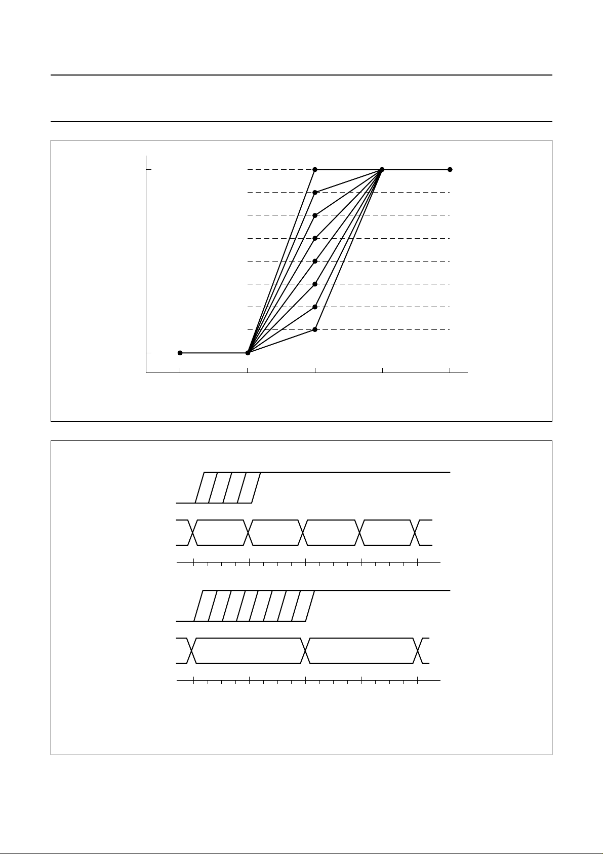
Fast insertion mode:
Fast insertion is applied by FSI pulse to ensure correct
timing. The RGB source signal is matrixed into UV and
inserted into the CVBS or Y/C source signal after two field
periods if FSI pulses are received. The output FSO is set
to HIGH during a determined insertion window (screen
plain minus 6 % of horizontal and vertical deflection).
Switch over depends on the phase of FSI in relation to the
valid pixel sequence depending on the phase-different
weighting factors. They are applied to the original and the
April 1993 8
inserted UV data (Figures 6 and 7)
The control signals for the front end (Table 1) MUXC, FSO,
status bits FSST1 and FSST0 (outputs GPSW2 and
GPSW1) are generated by the SAA7151B.
The amplitude of chrominance and colour-difference
signals are scaled down by factor 2 to avoid overloading of
the chrominance analog-to-digital converter. The
amplitudes are reduced in the TDA8446 by signals on lines
GPSW2 and GPSW1.
Page 9

Philips Semiconductors Product specification
Digital multistandard colour decoder with
SCART interface (DMSD2-SCART)
Luminance processing
The luminance input signal, a digital CVBS format or an
8-bit luminance format (S-Video), is fed through a sample
rate converter to reduce the data rate to 13.5 MHz (Fig.5).
Sample rate is converted by means of a switchable
pre-filter. High frequency components are emphasized to
compensate for loss in the following chrominance trap
filter. This chrominance trap filter (fo= 4.43 MHz or
fo= 3.58 MHz centre frequency selectable) eliminates the
most of the colour carrier signal, therefore, it must be
bypassed for S-Video signals.
The high frequency components of the luminance signal
can be “peaked” in two bandpass filters with selectable
transfer characteristic. A coring circuit (±1 LSB) can
improve the signal, this signal is then added to the original
signal. A switchable amplifier achieves a common DC
amplification, because the DC gains are different in both
chrominance trap modes. Additionally, a cut-off sync pulse
is generated for the original signal in both modes.
Synchronization
The luminance output signal is fed to the synchronization
stage. Its bandwidth is reduced to 1 MHz in a low-pass
filter (sync pre-filter). The sync pulses are sliced and fed to
the phase detectors to be compared with the sub-divided
clock frequency. The resulting output signal is applied to
the loop filter to accumulate all phase deviations. There
are three groups of output timing signals:
a. signals related to data output signals (HREF)
b. signals related to the input signals (HSY, and HCL)
c. signals related to the internal sync phase
All horizontal timings are derived from the main counter,
which represents the internal sync phase. The HREF
signal only with its critical timing is phase-compensated in
relationship to the data output signal. Future circuit
improvements could slightly influence the processing
SAA7151B
delays of some internal stages to achieve a changed
timing due to the timing groups b and c.
The HREF signal only controls the data multiplexer phase
and the data output signals.
All timings of the following diagrams are measured with
nominal input signals, for example coming from a pattern
generator. Processing delay times are taken between
input and data output, respectively between internal sync
reference (main counter = 0) and the rising edge of HREF.
Line locked clock frequency
LFCO is required in an external PLL (SAA7157) to
generate the line-locked clock frequency LL27 and CREF.
YUV-bus, digital outputs
The 16-bit YUV-bus transfers digital data from the output
interfaces to a feature box, or to the digital-to-analog
converter (DAC). Outputs are controlled via the I
normal selections, or they are controlled by output enable
chain (FEIN, pin 64). The YUV-bus data rate 13.5 MHz.
Timing is achieved by marking each second positive rising
edge of the clock LL27 synchronized by CREF.
YUV-bus formats
4:2:2 and 4:1:1
The output signals Y7 to Y0 are the bits of the digital
luminance signal. The output signals UV7 to UV0 are the
bits of the digital colour-difference signal. The frames in
the Tables 2 and 3 are the time to transfer a full set of
samples. In case of 4:2:2 format two luminance samples
are transmitted in comparison to one U and one V sample
within one frame. The time frames are controlled by the
HREF signal, which determines the correct UV data
phase. The YUV data outputs can be enabled or set to
3-state position by means of the FEIN signal. FEIN = LOW
enables the output; HIGH on this pin forces the Y and U/V
outputs to a high-impedance state (Fig.6).
2
C-bus in
April 1993 9
Page 10
Philips Semiconductors Product specification
Digital multistandard colour decoder with
SCART interface (DMSD2-SCART)
UV
(7-0)
AND
FAST SWITCH
UV
HREF
FEIN
42
64
OUTPUT
INTERFACE
FORMATTER
AND OUTPUT
WEIGHTING
Y
COMB FILTER
LOW-
(7-0)
AND
UV
SECAM
PASS
FILTER
RECOMBINATION
OFTS
COLO
UV
CCIR
SUVI
COFF
OEDY
OEHS
OEDC
FILTER
CLOCHE
(SECAM)
CHSB
GPSW2
GPSW1
24
25
PHASE
SCART
AND
DEMODULATOR
MUXC
FSO
656668
CONTROL
INTERFACE
DETECTOR
AMPLITUDE
FSI
SAA7151B
MEH294
FSAU
FSDL(2-0)
GPSI(2-1)
OFTS
FSIV
FSST
SXCR
DIFFERENTIATOR
DE-EMPHASIS
handbook, full pagewidth
44
CPI
clamping
OFTS, IPBP
CGFX, AMPF(3-0)
TIME
INTERPOLATION
DELAY
COMPENSATION
UV
OFFSET
STOP FILTER,
CHROMINANCE
COMPENSATION
OSCE
GAIN
AMPLIFIER
CONTROLLED
LOW-
PASS
FILTER
QUADRATURE
DEMODULATOR
C
BANDPASS
CHROMINANCE
INPUT
INTERFACE
PI2
LOOP
FILTER
CKTS (4-0)
CHCV (7-0)
CKTO (4-0)
AND DIVIDER
OSCILLATOR (DTO1)
HUEC(7-0)
UVSS
CDPO
YDEL0
CDMO
LFIS (2-1)
FISE
DISCRETE TIME
CHRS
BYPS
32
LOOP
FILTER
PI1
BURST GATE
ACCUMULATOR
SAA7151B
SEQUENCE
PROCESSOR
SEQAPLSE(7-0)
SESE(7-0)
CDVI
CHROMINANCE
STANDARD
DETECTION
CDET
ASTD
CSTD(2-0)
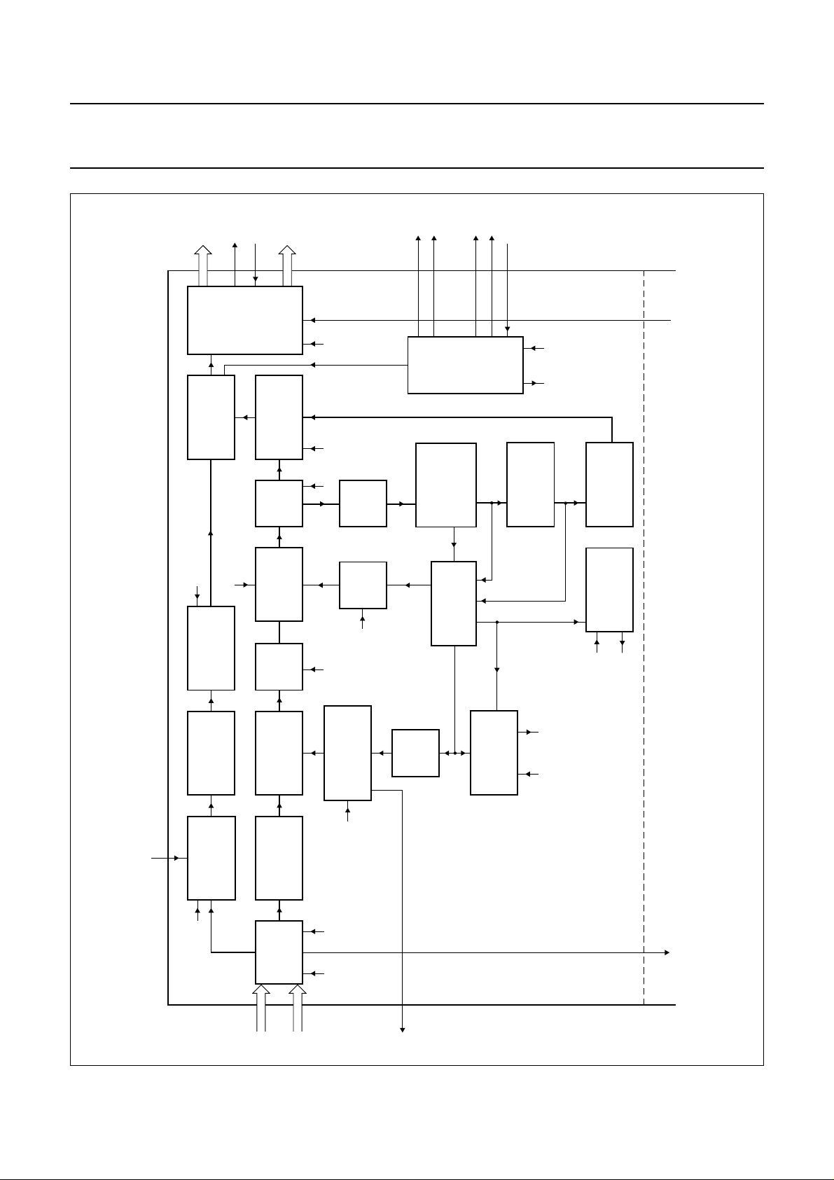
Fig.4 Detailed block diagram; continued in Fig.5.
to luminance from luminance
(7-0)
CUV
CVBS
(7-0)
RTCO
April 1993 10
Page 11

Philips Semiconductors Product specification
Digital multistandard colour decoder with
SCART interface (DMSD2-SCART)
(3-1)
YDEL
COMPENSATION
VARIABLE DELAY
AND
WEIGHTING
ADDING STAGE
(1-0)
APER
CREF
LL27
4
27
CLOCK
GENERATOR
LINE-LOCKED
DELAY
PROGRAMMABLE
XTAL
XTALI
33
34
CLOCK
CRYSTAL
GENERATOR
(DTO2)
OSCILLATOR
DISCRETE TIME
SAA7151B
MEH295
DAC
ndbook, full pagewidth
from input interface to output interface
CORING
FILTER
VARIABLE
BANDPASS
TRAP
CHROMINANCE
PRE-FILTER
CONVERTER
SAMPLE RATE
CORI
PREF
BYPS
(1-0)
BYPS BPSS
PREF
OFFSET
MATCHING
AMPLIFIER
LUMINANCE
COMPENSATION
LOOP
FILTER
COARSE
PHASE DETECTOR
FINE
PHASE DETECTOR
SYNC SLICER
SYNC
PRE-FILTER
HPLL
HLCK
HLCK
VTRC
HCLB (7-0)
HCLS (7-0)
HSYB (7-0)
HSYS (7-0)
SCEN
SAA7151B
VNOI (1-0)
WIND
BOFL
BFON
SYNC
HPHI (7-0)
IDEL (7-0)
OEVS
OEHS
FSEL
41
HLCK
C-BUS
2
I
AUFD
VERTICAL
PROCESSOR
COUNTER
CONTROL
40
FIDT
39 36
ODD
29 30 31
HSY VS HS LFCO
26
HCLGPSW0
Fig.5 Detailed block diagram; continued from Fig.4.
63
43
April 1993 11
SCL
SDA
IICSA
Page 12

Philips Semiconductors Product specification
Digital multistandard colour decoder with
SAA7151B
SCART interface (DMSD2-SCART)
Table 2 for the 4:2:2 format (720 pixels per line). The quoted frequencies are valid on the YUV-bus. The time
frames are controlled by the HREF signal.
OUTPUT PIXEL BYTE SEQUENCE
Y0 (LSB) Y0 Y0 Y0 Y0 Y0 Y0
Y1 Y1 Y1 Y1 Y1 Y1 Y1
Y2 Y2 Y2 Y2 Y2 Y2 Y2
Y3 Y3 Y3 Y3 Y3 Y3 Y3
Y4 Y4 Y4 Y4 Y4 Y4 Y4
Y5 Y5 Y5 Y5 Y5 Y5 Y5
Y6 Y6 Y6 Y6 Y6 Y6 Y6
Y7 (MSB) Y7 Y7 Y7 Y7 Y7 Y7
UV0 (LSB) U0 V0 U0 V0 U0 V0
UV1 U1 V1 U1 V1 U1 V1
UV2 U2 V2 U2 V2 U2 V2
UV3 U3 V3 U3 V3 U3 V3
UV4 U4 V4 U4 V4 U4 V4
UV5 U5 V5 U5 V5 U5 V5
UV6 U6 V6 U6 V6 U6 V6
UV7 (MSB) U7 V7 U7 V7 U7 V7
Y frame 012345
UV frame 0 2 4
Table 3 for the 4:1:1 format (720 pixels per line). The quoted frequencies are valid on the YUV-bus. The time
frames are controlled by the HREF signal.
OUTPUT PIXEL BYTE SEQUENCE
Y0 (LSB) Y0 Y0 Y0 Y0 Y0 Y0 Y0 Y0
Y1 Y1 Y1 Y1 Y1 Y1 Y1 Y1 Y1
Y2 Y2 Y2 Y2 Y2 Y2 Y2 Y2 Y2
Y3 Y3 Y3 Y3 Y3 Y3 Y3 Y3 Y3
Y4 Y4 Y4 Y4 Y4 Y4 Y4 Y4 Y4
Y5 Y5 Y5 Y5 Y5 Y5 Y5 Y5 Y5
Y6 Y6 Y6 Y6 Y6 Y6 Y6 Y6 Y6
Y7 (MSB) Y7 Y7 Y7 Y7 Y7 Y7 Y7 Y7
UV0 (LSB) 0 0 0 0 0 0 0 0
UV1 0 0 0 0 0 0 0 0
UV2 0 0 0 0 0 0 0 0
UV3 0 0 0 0 0 0 0 0
UV4 V6 V4 V2 V0 V6 V4 V2 V0
UV5 V7 V5 V3 V1 V7 V5 V3 V1
UV6 U6 U4 U2 U0 U6 U4 U2 U0
UV7 (MSB) U7 U5 U3 U1 U7 U5 U3 U1
Y frame 0 1 2 3 4 5 6 7
UV frame 0 4
April 1993 12
Page 13
Philips Semiconductors Product specification
Digital multistandard colour decoder with
SAA7151B
SCART interface (DMSD2-SCART)
Signal levels (Figures 12, 13 and 14) The nominal input and output signal levels are defined by a colour bar signal with 75 % colour, 100 % saturation and
100 % luminance amplitude (EBU colour bar).
CUV-bus input format
The CUV-bus transfers the digital chrominance/colour-difference signals from the ADC to the SAA7151B (Fig.6; Table 1):
• normal mode for digital chrominance transmission.
• UV colour-difference mode for colour-difference signals UV (out of matrixed RGB signals)
• FS mode (fast switch mode; UV inserted into chrominance signal C with addition of the two signal spectra).
RTCO output
The RTCO output signal (Fig.10) contains serialized information about actual clock frequency, subcarrier frequency and
PAL/SECAM sequence. This signal may preferably be used with the frequency-locked digital video encoder SAA7199B.
handbook, full pagewidth
LL27
CREF
HREF
FEIN
YUV
to 3-state
t
OH
t
HD
t
SU
from 3-state
Fig.6 Timing example of fast enable input (FEIN).
t
OS
MEH548
April 1993 13
Page 14

Philips Semiconductors Product specification
Digital multistandard colour decoder with
SCART interface (DMSD2-SCART)
handbook, full pagewidth
LL27 clock
LL13.5 clock
MUXC
012
0
SAA7151B
345
12
Normal mode (chrominance pixel byte sequence)
chrominance
UV colour-difference mode (UV pixel byte sequence)
colour-
difference
valid colourdifference
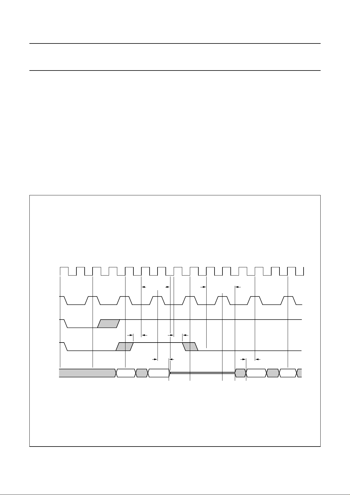
Fast switch mode (data insertion)
CUV
valid CUV
C0
V0
U0 V1 U3
(V0 + C0)/2
C1
V1
(V1 + C1)/2
C2
U2
(1) (1) (1)
(U2 + C2)/2
(1) (1) (1)
(V1 + C1)/2 (U3 + C3)/2
C3
U3
(U3 + C3)/2
C4
V4
(V4 + C0)/2
C5
V5
V5
(V5 + C5)/2
(V5 + C5)/2
MEH332
Fig.7 CUV input formats.
(1) each second sample only after a MUXC change is taken for down-sampling to 13.5 MHz to reduce
cross-talk components between U and V signals.
April 1993 14
Page 15
Philips Semiconductors Product specification
Digital multistandard colour decoder with
SCART interface (DMSD2-SCART)
handbook, full pagewidth
new
old
0 old + 1 new
1/8 old + 7/8 new
1/4 old + 3/4 new
3/8 old + 5/8 new
1/2 old + 1/2 new
5/8 old + 3/8 new
3/4 old + 1/4 new
7/8 old + 1/8 new
T(n−2) T(n−1) T(n)
Note: in 4:2:2 format weighting
in 1/4 steps only.
T(n+1) T(n+2)
SAA7151B
MEH307
handbook, full pagewidth
FS
UV
LL6.75
LL27
FS
UV
LL3.375
LL27
Fig.8 Addition of weighted components.
1
3/4 1/2 1/4 fast switch weighting for 4:2:2 format
U0, V0 U1, V1
01
012
013
01234
34
5678910111213141516
1 7/8 3/4 5/8 1/2 3/8 1/4 1/8
U0, V0
5678910111213141516
U2, V2 U3, V3
234
fast switch weighting for 4:1:1 format
U1, V1
MEH308
Fig.9 Weighting factors of fast switching for 4:2:2 and 4:1:1 formats.
April 1993 15
Page 16

Philips Semiconductors Product specification
Digital multistandard colour decoder with
SCART interface (DMSD2-SCART)
handbook, full pagewidth
Byte number for pixels:
handbook, full pagewidth
LL27
CREF
HREF
Y signal
50/60 Hz
U and V signal
LL27
start of
active line
012345
U0 V0 U2 V2 U4 V4
SAA7151B
67
U6 V6
MEH297
CREF
HREF
Byte number for pixels:
Y signal
50/60 Hz
U and V signal
714 715 716 717 718 719
U714 V714 U716 V716 U718 V718
Fig.10 Line control by HREF in 4:2:2 format for 50 Hz and 60 Hz systems.
handbook, full pagewidth
RTCO
(1)
Sequence bit:
SECAM: 0 equals DB-line
PAL: 0 equals (R-Y) line normal
NTSC: 0 (no change)
(2)
Reserve bits: 236 for 50 Hz systems; 233 for 60 Hz systems
1 equals DR-line
1 equals (R-Y) line inverted
H/L transition
(counter start)
128 clocks
048 1419
HPLL
increment
bits 13 to 0
4 bits
reserve
bit
time slot
(LL27/4)
152113 0 20 10 5
Fig.11 RTCO timing.
end of
active line
FSCPLL
increment
bits 21 to 0
valid
not valid
5 bits
reserve
10
61 67
MEH298
sequence bit
reserved
MEH341
(1)
(2)
April 1993 16
Page 17

Philips Semiconductors Product specification
Digital multistandard colour decoder with
SCART interface (DMSD2-SCART)
handbook, full pagewidth
Condition: Nominal input signal, 50 Hz
(a) 1st field
625 1 2 3 4 5
input CVBS
HREF
VS
ODD
(b) 2nd field
313 314 315 316 317 318 319 320 321
input CVBS
SAA7151B
6
789
503 × 2/LL27
2 × 2/LL27
HREF
VS
ODD
71 × 2/LL27
2 × 2/LL27
MEH335
Fig.12 Vertical timing diagram at 50 Hz.
April 1993 17
Page 18

Philips Semiconductors Product specification
Digital multistandard colour decoder with
SCART interface (DMSD2-SCART)
handbook, full pagewidth
Condition: Nominal input signal, 60 Hz
(a) 1st field
525 1 2 3 4 5
input CVBS
HREF
VS
ODD
(b) 2nd field
263 264 265 266 267 268 269 270 271
input CVBS
SAA7151B
6
789
491 × 2/LL27
2 × 2/LL27
HREF
VS
ODD
59 × 2/LL27
2 × 2/LL27
MEH336
Fig.13 Vertical timing diagram at 60 Hz.
April 1993 18
Page 19

Philips Semiconductors Product specification
Digital multistandard colour decoder with
SCART interface (DMSD2-SCART)
handbook, full pagewidth
+127
+106
+95
0
−52
−64
−91
−103
−128
−132
reserved
luminance
50 Hz mode
sync
luminance
60 Hz mode
chrominance
60 Hz mode
chrominance
50 Hz mode
blanking level
clipped
(a) CVBS input signal range.
+127
+105
+100
+76
−76
−91
−103
−128
C
chrominance
0
(b) CUV input signal range
(U and V out of RGB;
in FS mode ranges × 0.5).
SAA7151B
V
U
component of
colour-difference
signal
+255
+235
luminance signal
output range
+128
+16
0
(c) Y output signal range.
Notes:1. All levels related to EBU colour bar.
2. Values in decimal at 100% luminance and 75% chrominance amplitude
white 100%
black
+127
+100
0
U-component
output signal range
−101
−128
(d) U output signal range (B-Y).
Fig.14 Input and output signal ranges in DTV mode (digital TV).
blue 75%
yellow 75%
+127
+105
0
V-component
output signal range
−106
−128
(e) V output signal range (R-Y).
red 75%
cyan 75%
MEH299
April 1993 19
Page 20

Philips Semiconductors Product specification
Digital multistandard colour decoder with
SCART interface (DMSD2-SCART)
handbook, full pagewidth
+127
+106
+95
0
−52
−64
−91
−103
−128
−132
reserved
luminance
50 Hz mode
sync
100% white
luminance
60 Hz mode
chrominance
60 Hz mode
chrominance
50 Hz mode
blanking level
clipped
(a) CVBS input signal range.
+127
+84
+76
−76
−84
−128
C
chrominance
0
(b) CUV input signal range
(U and V out of RGB;
in FS mode ranges × 0.5).
SAA7151B
V
U
component of
colour-difference
signal
+255
+235
luminance signal
output range
+128
+16
0
(c) Y output signal range.
Notes: 1. All levels are related to EBU colour bar.
2. Values in decimal at 100 % luminance and 75 % chrominance amplitude.
3. For SECAM input signals the CCIR levels will be exceeded.
white 100%
black
+255
+212
+128
U-component
output signal range
+44
0
(d) U output signal range (B-Y).
Fig.15 Input and output signal ranges in CCIR mode.
blue 75%
yellow 75%
+255
+212
+128
V-component
output signal range
+44
0
(e) V output signal range (R-Y).
red 75%
cyan 75%
MEH300
April 1993 20
Page 21

Philips Semiconductors Product specification
Digital multistandard colour decoder with
SCART interface (DMSD2-SCART)
Y
out
63 × 2/LL27
0
0
83.5 × 2/LL27
(1)
handbook, full pagewidth
CVBS
HSY
step size 2/LL27
HSY
programming
range
(step size: 2/LLC)
HCL
HCL
programming
range
(step size: 2/LL27)
Y-output
+191
+127
+235
+16
0
burst
4 × 2/LL27 (50 HZ)
10 × 2/LL27 (60 HZ)
SAA7151B
−64
−128
HREF position
HREF
720 × 2/LL27
HS
HS
programming range
(step size: 8/LL27)
(1) the processing delay will be influenced in future enhancements.
(1)
the processing delay will be ifluenced in future enhancements
0
Fig.16 Horizontal sync and clamping timing for 50/60 Hz (signals HSY, HCL, HREF and HS).
16 × 2/LL27 (50 HZ)
12 × 2/LL27 (60 HZ)
64 × 2/LL27
0......719
144 × 2/LL27 (50 HZ)
138 × 2/LL27 (60 HZ)
HREF length fix
−432+431
MEH549
April 1993 21
Page 22

Philips Semiconductors Product specification
Digital multistandard colour decoder with
SAA7151B
SCART interface (DMSD2-SCART)
LIMITING VALUES
In accordance with the Absolute Maximum Rating System (IEC 134); ground pins 19, 35, 38, 51 and 67 as well as
supply pins 5, 18, 28, 37 and 52 connected together.
SYMBOL PARAMETER MIN. MAX. UNIT
V
DD
V
diff GND
V
I
V
O
P
tot
T
stg
T
amb
V
ESD
Note
1. Equivalent to discharging a 100 pF capacitor through a 1.5 kΩ series resistor; inputs and outputs are protected
against electrostatic discharge in normal handling. Normal precautions appropriate to handle MOS devices is
recommended (
supply voltage (pins 5, 18, 28, 37, 52) −0.5 7.0 V
difference voltage V
SS A
− V
SS(1 to 4)
−±100 mV
voltage on all inputs −0.5 VDD+0.5 V
voltage on all outputs (I
= 20 mA) −0.5 VDD+0.5 V
O max
total power dissipation − 2.5 W
storage temperature range −65 150 °C
operating ambient temperature range 0 70 °C
electrostatic handling
“Handling MOS Devices”
(1)
for all pins −±2000 V
).
April 1993 22
Page 23

Philips Semiconductors Product specification
Digital multistandard colour decoder with
SAA7151B
SCART interface (DMSD2-SCART)
CHARACTERISTICS
= 4.5 to 5.5 V; T
V
DD
SYMBOL PARAMETER CONDITIONS MIN. TYP. MAX. UNIT
V
DD
I
DD
2
C-bus, SDA and SCL (pins 40 and 41)
I
V
IL
V
IH
I
40, 41
I
ACK
V
OL
supply voltage range (pins 5, 18, 28, 37, 52) 4.5 5 5.5 V
total supply current (pins 5, 18, 28, 37, 52) VDD= 5 V; inputs LOW;
input voltage LOW −0.5 − 1.5 V
input voltage HIGH 3 − VDD+0.5 V
input current −− ±10 µA
output current on pin 40 acknowledge 3 −−mA
output voltage at acknowledge I40=3mA −− 0.4 V
Data, clock and control inputs (pins 3, 4, 6 to 17, 20 to 23, 27, 34, 64 and 68); Figures 14 and 15
V
IL
V
IH
V
IL
V
IH
I
leak
C
I
t
SU.DAT
t
HD.DAT
LL27 input voltage (pin 27) LOW −0.5 − 0.6 V
other input voltages LOW −0.5 − 0.8 V
input leakage current −− 10 µA
input capacitance data inputs; note 1 −− 8pF
input data set-up time Fig.17 11 −−ns
input data hold time 3 −−ns
YUV-bus, HREF and VS outputs (pins 30, 42, 45 to 50 and pins 53 to 62), Figures 10, 14 and 15
V
V
C
OL
OH
L
output voltage LOW notes 1 and 2 0 − 0.6 V
output voltage HIGH 2.4 − V
load capacitor 15 − 50 pF
LFCO output (pin 36)
V
o
V
36
output signal (peak-to-peak value) note 2 1.4 − 2.6 V
output voltage range 1 − V
Control outputs (pins 24 to 26, 29, 31, 32, 33, 39, 63, 65 and 66); Figures 12, 16 and 17
V
V
C
OL
OH
L
output voltage LOW notes 1 and 2 0 − 0.6 V
output voltage HIGH 2.4 − V
load capacitor 7.5 − 25 pF
= 0 to 70 °C unless otherwise specified.
amb
outputs not connected − 100 250 mA
HIGH 2.4 − VDD+0.5 V
HIGH 2.0 − VDD+0.5 V
I/O high-impedance −− 8pF
clock inputs −− 10 pF
DD
DD
DD
V
V
V
April 1993 23
Page 24

Philips Semiconductors Product specification
Digital multistandard colour decoder with
SAA7151B
SCART interface (DMSD2-SCART)
SYMBOL PARAMETER CONDITIONS MIN. TYP. MAX. UNIT
Timing of YUV-bus and control outputs
t
t
t
t
OH
OS
SZ
ZS
output signal hold time YUV, HREF, VS
output set-up time YUV, HREF, VS
data output disable transition time to 3-state condition 22 −−ns
data output enable transition time from 3-state condition 20 −−ns
Chrominance PLL
f
C
catching range ±400 −−Hz
Crystal oscillator
f
n
∆f/f
n
nominal frequency 3rd harmonic − 24.576 − MHz
permissible deviation f
temperature deviation from f
n
n
X1 crystal specification:
temperature range T
load capacitance C
series resonance resistance R
motional capacitance C
parallel capacitance C
amb
L
S
1
0
Line locked clock input LL27 (pin 27)
t
LL27
t
p
t
r
t
f
cycle time note 4 35 − 39 ns
duty factor t
rise time −− 5ns
fall time −− 6ns
Notes
1. Data output signals are Y7 to Y0 and UV7 to UV0. All other are control signals.
2. Levels are measured with load circuit. YUV-bus, HREF and VS outputs with 1.2 kΩ in parallel to 50 pF at 3 V
(TTL load);
LFCO output with 10 kΩ in parallel to 15 pF and other outputs with 1.2 kΩ in parallel to 25 pF at 3 V (TTL load).
3. Recommended crystal: Philips 4322 143 05291.
4. tSU, tHD, tOH and tOD include tr and tf.
Figures 10, 12 and 13
at CL= 15 pF; 13 −−ns
controls at C
= 7.5 pF 13 −−ns
L
at CL= 50 pF; 20 −−ns
controls at C
=25pF 20 −−ns
L
Figures 19 and 20; note 3
−− ±50 10
−− ±20 10
0 − 70 °C
8 −−pF
− 40 80 Ω
− 1.5±20% − fF
− 3.5±20% − pF
Fig.9 and 17
LL27H/tLL27
40 50 60 %
−6
−6
April 1993 24
Page 25

Philips Semiconductors Product specification
Digital multistandard colour decoder with
SAA7151B
SCART interface (DMSD2-SCART)
Table 4 High-impedance control for YUV-bus (Fig.17)
OEDY OEDC FEIN Y(7:0) UV(7:0)
00 0 Z Z
0 1 0 Z active
1 0 0 active Z
11 0 Z Z
XX 1 Z Z
handbook, full pagewidth
clock input LL27
input data
t
LL27H
t
SU
t
HD
not valid
t
LL27
2.4 V
1.5 V
0.6 V
t
f
t
r
2.0 V
0.8 V
input CREF
output data
input FEIN
t
ZS
t
t
OS
t
SZ
OH
not valid
Fig.17 Data input and output timing diagram.
t
SU
t
t
SUtHD
2.0 V
0.8 V
HD
2.4 V
0.6 V
2.4 V
0.6 V
MEH550
April 1993 25
Page 26

Philips Semiconductors Product specification
Digital multistandard colour decoder with
SCART interface (DMSD2-SCART)
handbook, full pagewidth
1 nF
24.576 MHz
(3rd harmonic)
X1
10 µH
(±20%)
10 pF
10 pF
XTAL
XTALI
33
SAA7151B
34
(a) (b)
Fig.18 Oscillator application (a) and optional clock from external (b).
XTAL
XTALI
SAA7151B
33
SAA7151B
34
MEH302
April 1993 26
Page 27

Philips Semiconductors Product specification
Digital multistandard colour decoder with
SCART interface (DMSD2-SCART)
handbook, full pagewidth
CPI
digital
+5 V
chrominance
CUV7 to CUV0
luminance
CVBS7 to CVBS0
X1 :
Philips 4322 143 05291
X1 24.576 MHz
12
10
pF
µH
1 nF
digital
0.1 µF
0.1 µF
0.1 µF
0.1 µF
V
12
pF
MUXC
FSO
GPSW1
GPSW2
RESN
LL27A
CREF
LL27B
LL13A
LL13B
DD
CUV0
CUV1
CUV2
CUV3
CUV4
CUV5
CUV6
CUV7
L0
L1
L2
L3
L4
L5
L6
L7
RESN
V
SS
67 51 38 19 44
5
18
28
52
6
7
8
9
10
11
12
13
14
15
16
17
20
21
22
23
33
34
3
27
4
24
25 36 65 66
LFCO
11
19
16
12
15
10
14
7
20
SAA7151B
SAA7157
5
2
3
4
8
17
1
6
9
13
18
SAA7151B
UV0
62
UV1
61
UV2
60
UV3
59
UV4
58
UV5
57
UV6
56
UV7
55
Y0
54
Y1
53
Y2
50
Y3
49
Y4
48
Y5
47
Y6
46
Y7
45
V
SSA
V
DDA
0.1 µF
0.1 µF
RTCO
HS
VS
HSY
HCL
HREF
SCL
SDA
ODD
GPSW0
FEIN
IICSA
digital
680 Ω
0.1 µF
f > 13 MHz
10 µF
analog
MEH328
32
31
30
29
26
42
41
40
39
63
64
43
2
1
35
FSI
0.1
µF
digital
37
2.2 µH
68
+5 V
0.1
µF
2
I
C-bus
YUV-bus
BAT45
V
DD analog
V
DD digital
UV7 to UV0
Y7 to Y0
(from SCART)
FS
150
pF
680
Ω
+5 V
+5 V
75
Ω
Fig.19 Application of SAA7151B.
April 1993 27
Page 28

Philips Semiconductors Product specification
Digital multistandard colour decoder with
SCART interface (DMSD2-SCART)
handbook, full pagewidth
sync
from SCART connector
FS
B
G
R
+12 V
kΩ
47
2.2 µH
4.7 kΩ
1 nF
75
Ω
75 Ω
75 Ω
75 Ω
to SAA7151B
0.1 µF
chrominance
bandpass filter
0.1 µF
0.1 µF
0.1 µF
4.7 µF
C
1 kΩ
22
µF
1
2
3
4
5
TDA8446
6
7
8
9
10
20
19
18
17
16
15
14
13
12
11
0.15 µF
V
P
CVBS/Y
sync
0.1 µF
0.1 µF
+12 V
SAA7151B
U signal
Y signal
V signal
GPSW2
FSO
C signal
HCL
GPSW1
CLO
from / to TDA8708/09
SCL
SDA
C
(chrominance)
CVBS
Y
2
C-bus
I
75 Ω
75 Ω
75 Ω
75 Ω
unused signal
outputs
22 µF
0.1 µF
0.1 µF
0.1 µF
1
2
3
4
5
6
7
8
9
10
TDA8540
20
19
18
150 Ω
17
16
22 µF
15
14
22 Ω
13
12
11
0.1
µF
150
Ω
C
V
P
+8 V
10 µF
22 Ω
0.1 µF
Fig.20 Application of input signal selecting (SCART interface).
7808
stabilizer
1.6 kΩ
220 pF
330 Ω
SCL
SDA
(to SAA7151B)
10 kΩ
10 kΩ
audio
source
control
MEH330
+5 V
April 1993 28
Page 29

Philips Semiconductors Product specification
Digital multistandard colour decoder with
SCART interface (DMSD2-SCART)
from/to SAA7151B
GPSW2
DDA
V
NOR
9
16
BC547
MUXC
11
13
6.8 kΩ
2
kΩ
33 pF
14
HCT4053
µF
0.1
1
nF
Ω
220
4.7
2
CUV(7-0)
CUV0
CUV1
14
1316121711
1 kΩ
15
VIN1
VIN0
1 µF
1 µF
4.7 µF
10 µF
1.5 kΩ
4
7
10
kΩ
6, 8,
100
35
12
1.5 kΩ
1 nF
220 Ω
BC547
10 µF
µF
kΩ
2
kΩ
CUV2
18
VIN2
digital
CUV3
1.2 kΩ
1415
4.7 µF
68
9
10
19
20
1 µF
1 mH
CVBS0
CVBS1
1316121711
VIN0
VIN1
1 µF
pF
8
21
3.3 kΩ
CVBS2
VIN2
1 µF
0.1 µF
DDO
V
7
TDA8709A
22
DDA
V
CVBS3
10
18
19
0.1 µF
DDD
V
CLK
6
23
0.22 µF
0.1 µF
digital
9
20
1 µF
GPSW1
handbook, full pagewidth
5
24
0.1
0.1
8
21
2.2 kΩ
CUV4
4
25
0.1 µF
µF
µF
DDO
V
7
TDA8708A
22
DDA
V
CUV5
3
26
6.2 kΩ
68 pF
DDD
V
0.1 µF
6
23
22
analog
0.22 µF
Ω
CUV6
2
27
CLK
SAA7151B
Ω
120
CUV7
1
28
3 kΩ
Ω
22
CVBS4
5
24
10 µF
CPI
1 kΩ
5.6 Ω
5.6 Ω
Ω
120
CVBS3
CVBS2
4
3
2
25
26
27
CVBS(7-0)
CVBS7
1
28
10 Ω
HCL
analog
HSY
MEH329
5.6 Ω
Fig.21 Application circuit analog-to-digital conversions.
to pin 8
1 kΩ
V signal
from pin 15
2 MHz
low-pass
filters
1 kΩ
U signal
from pin 17
C signal
from pin 11
Y or CVBS
from pin 16
from/to TDA8446
680 Ω
April 1993 29
(+5 V)
filter
5 MHz low-pass
5.6 Ω
CLO from pin 4
of TDA8446
HCL to pin 9
of TDA8446
LL27A
UV gain level for CCIR
+5 V (analog supply)
+5 V (digital supply)
Page 30

Philips Semiconductors Product specification
Digital multistandard colour decoder with
SAA7151B
SCART interface (DMSD2-SCART)
I2C-BUS FORMAT
S SLAVE ADDRESS A SUBADDRESS A DATA0 A DATAn A P
S = start condition
SLAVE
ADDRESS
A = acknowledge, generated by the slave
SUBADDRESS
DATA = data byte (Table 5)
P = stop condition
X = read/write control bit
Note
1. If more than 1 byte DATA are transmitted, then auto-increment of the subaddress is performed.
Remarks: - Prior to reset of the IC all outputs are undefined.
- After power-on reset, the control register 12 (hex) is set to 00 (hex).
= 1000 101X (IICSA = LOW) or 1000 111X (IICSA = HIGH)
(1)
= subaddress byte (Table 5)
X = 0, order to write (the circuit is slave receiver)
X = 1, order to read (the circuit is slave transmitter)
April 1993 30
Page 31

Philips Semiconductors Product specification
Digital multistandard colour decoder with
SAA7151B
SCART interface (DMSD2-SCART)
Table 5 I2C-bus; DATA for status byte (X in address byte = 1; slave address 8B (hex) at IICSA = LOW or 8F (hex) at
IICSA = HIGH)
FUNCTION DATA
D7 D6 D5 D4 D3 D2 D1 D0
status byte STTC HLCK FIDT FSST1 FSST0 CDET2 CDET1 CDET0
Function of the bits:
STTC Status time constant (to be used for gogical combfilter SAA7152)
0 = TV mode; 1 = VCR mode
HLCK Horizontal PLL information: 0 = HPLL locked; 1 = HPLL unlocked
FIDT Field information 0 = 50 Hz system detected; 1 = 60 Hz system detected
−-−-−-−-−-−-−-−-−-−-−-−-−-−-−-−-−-−-−-−-−-−-−-−-−-−-−-−-−-−-−-−-−-−-−-−-−-−-−-−-−-−-−-−-−-−-−-−-−-−-−-−-−-−-−-−-−-−-−
FSST1 to FSST0 Fast switching output mode: FSST1 FSST0 mode
0
0
1
1
−-−-−-−-−-−-−-−-−-−-−-−-−-−-−-−-−-−-−-−-−-−-−-−-−-−-−-−-−-−-−-−-−-−-−-−-−-−-−-−-−-−-−-−-−-−-−-−-−-−-−-−-−-−-−-−-−-−-−
CDET2 to CDET0 Identified colour standard CDET2 CDET2 CDET2 standard
0
0
0
0
0
1
0
1
0
0
1
1
RGB; FSI = HIGH (pin 68)
Y/C; FSI = LOW (pin 68)
fast switching (toggle)
not used
0
1
0
1
PAL-B/G, -H, -I; 50 Hz
PAL-N; 50 Hz
SECAM; 50 Hz
PAL-M; 60 Hz
1
1
1
1
0
0
1
1
0
1
0
1
PAL 4.43; 60 Hz
NTSC-M; 60 Hz
NTSC 4.43; 60 Hz
black/white
April 1993 31
Page 32

Philips Semiconductors Product specification
Digital multistandard colour decoder with
SAA7151B
SCART interface (DMSD2-SCART)
Table 6 I2C-bus; subaddress and data bytes for writing (X in address byte = 0; slave address 8A (hex) at
IICSA = LOW or 8E at IICSA = HIGH)
function subaddress byte
increment delay
H-sync HSY begin
H-sync HSY stop
H-clamp HCL begin
H-clamp HCL stop
H-sync after PHI1
luminance control
hue control
miscellaneous controls #1
miscellaneous controls #2
PAL switch sensitivity
SECAM switch sensitivity
miscellaneous controls #3
miscellaneous controls #4
miscellaneous controls #5
miscellaneous controls #6
miscellaneous controls #7
chroma gain reference
miscellaneous controls #8
00
01
02
03
04
05
06
07
08
09
0A
0B
0C
0D
0E
0F10AUFD
1112CHCV7
D7 D6 D5 D4 D3 D2 D1 D0
IDEL7
HSYB7
HSYS7
HCLB7
HCLS7
HPHI7
BYPS
HUEC7
CSTD2
OSCE
PLSE7
SESE7
FSAU
COLO
CCIR
ASTD
OEDY
IDEL6
HSYB6
HSYS6
HCLB6
HCLS6
HPHI6
PREF
HUEC6
CSTD1
LFIS1
PLSE6
SESE6
GPSI2
CHSB
COFF
FSEL
OFTS
CHCV6
OEDC
IDEL5
HSYB5
HSYS5
HCLB5
HCLS5
HPHI5
BPSS1
HUEC5
CSTD0
LFIS0
PLSE5
SESE5
GPSI1
GPSW0
OEHS
HPLL
IPBP
CHCV5
VNOI1
data byte
IDEL4
HSYB4
HSYS4
HCLB4
HCLS4
HPHI4
BPSS0
HUEC4
CKTQ4
CKTS4
PLSE4
SESE4
CGFX
SUVI
OEVS
SCEN
CDVI
CHCV4
VNOI0
IDEL3
HSYB3
HSYS3
HCLB3
HCLS3
HPHI3
BFBY
HUEC3
CKTQ3
CKTS3
PLSE3
SESE3
AMPF3
SXCR
UVSS
VTRC
YDEL3
CHCV3
BFON
IDEL2
HSYB2
HSYS2
HCLB2
HCLS2
HPHI2
CORI
HUEC2
CKTQ2
CKTS2
PLSE2
SESE2
AMPF2
FSDL2
CHRS
MUIV
YDEL2
CHCV2
BOFL2
IDEL1
HSYB1
HSYS1
HCLB1
HCLS1
HPHI1
APER1
HUEC1
CKTQ1
CKTS1
PLSE1
SESE1
AMPF1
FSDL1
CDMO
FSIV
YDEL1
CHCV1
BOFL1
IDEL0
HSYB0
HSYS0
HCLB0
HCLS0
HPHI0
APER0
HUEC0
CKTQ0
CKTS0
PLSE0
SESE0
AMPF0
FSDL0
CDPO
WIND
YDEL0
CHCV0
BOFL0
April 1993 32
Page 33

Philips Semiconductors Product specification
Digital multistandard colour decoder with
SCART interface (DMSD2-SCART)
Function of the bits of Table 6
IDEL7 to IDEL0 Increment delay time, step size = 4/LL27 = 148 ns
“00” D7 D6 D5 D4 D3 D2 D1 D0 decimal number note
1111 1 111
1001 0 010 −16.3 µs (outside available range)
1001 0 001
0010 1 010 −31.7 µs (maximum value at FSEL = 1)
0010 1 001−215 −31.85 µs (outside central counter range
0010 1 000−216 −32.0 µs (maximum value at FSEL = 0
0010 0 111
0000 0 000 −37.9 µs (outside central counter
HSYB7 to HSYB0 Horizontal sync begin, step size = 2/LL27 = 74 ns
HSYS7 to HSYS0 Horizontal sync stop, step size = 2/LL27 = 74 ns
“01” and “02” D7 D6 D5 D4 D3 D2 D1 D0 decimal multiplier note
1011 1 111
0000 0 001 −74 ns
0 0 0 0 0 0 0 0 0 0 equals reference value
1111 1 111
1100 0 000 +4.7 µs
HCLB7 to HCLB0 Horizontal clamp begin, step size = 2/LL27 = 74 ns
HCLS7 to HCLS0 Horizontal clamp stop, step size = 2/LL27 = 74 ns
“03” and “04” D7 D6 D5 D4 D3 D2 D1 D0 decimal multiplier note
0111 1 111
0000 0 001 −74 ns
0 0 0 0 0 0 0 0 0 0 equals reference value
1111 1 111
1000 0 000 +9.5 µs (maximum positive value)
HPHI7 to HPHI0 Horizontal sync start, step size = 8/LL27 = 296 ns
“05” D7 D6 D5 D4 D3 D2 D1 D0 decimal multiplier note
001111101111101
0110 1 100
0000 0 001 −0.296 ns
0 0 0 0 0 0 0 0 0 0 equals reference value
111010111011101
110000100010000
−1 to −110
−111 to −214
−217 to −256
191 to 1
−1 to −64
127 to 1
−1 to −128
+127 to +109
1
+108 to +1
−1to−107
1
−108 to −128
0
(1)
minimum −148 ns
−16.44 µs
−32.148 µs (outside central counter range
−14.2 µs (maximum negative value)
+74 ns
−9.4 µs (maximum negative value)
+74 ns
) forbidden (outside available central
) counter range)
−32 µs (maximum negative value)
+0.296 µs
+31.7 µs (maximum positive value)
) forbidden (outside available central
) counter range)
at FSEL = 1
at FSEL = 0
SAA7151B
(2)
)
(2)
)
(2)
)
(2)
)
April 1993 33
Page 34

Philips Semiconductors Product specification
Digital multistandard colour decoder with
SAA7151B
SCART interface (DMSD2-SCART)
BYPS
“06”
PREF Use of pre-emphasis (to be used if chrominance trap is active):
−-−-−-−-−-−-−-−-−
BPSS1 to BPSS0 Aperture bandpass to select different centre frequencies (Figures 25 to 40):
BFBY Bandfilter bypass switching: 0 = bandfilter active; 1 = bandfilter bypassed
CORI Coring function: 0 = coring off; 1 = ±1 LSB coring
APER1 to APER0 Aperture factor (Figures 25 to 40):
HUE7 to HUE0
“07”
CSTD2 to CSTD0 Forced colour standard of input signal;
“08” CSTD2 CSTD1 CSTD0 standard
−-−-−-−-−-−-−-−-− -−-−-−-−-−-−-−-−-−-−-−-−-−-−-−-−-−-−-−-−-−-−-−-−-−-−-−-−-−-−-−-−-−-−-−-−-−-−-−-−-−-−-−-−-−-−-−-−-−
CKTQ4 to CKTQ0 Colour killer threshold QAM (PAL/NTSC):
Input mode select bit: 0 = CVBS mode (chroma trap active)
1 = S-Video mode (chroma trap by-passed)
0 = pre-filter bypassed; 1 = pre-filter on
-−-−-−-−-−-−-−-−-−-−-−-−-−-−-−-−-−-−-−-−-−-−-−-−-−-−-−-−-−-−-−-−-−-−-−-−-−-−-−-−-−-−-−-−-−-−-−-−-−-−-−-−
BPSS1 BPSS0 centre frequency
0
0
1
1
APER1 APER0 factor
0
0
1
1
Hue control from +178.6° to −180.0°, equals data bytes 7F to 80 (hex); 0° equals 00.
0
0
0
0
1
1
1
1
CKTQ4 CKTQ3 CKTQ2 CKTQ1 CKTQ0
1
1
0
1
0
0
0
1
0
1
0
1
0
1
0
0
1
1
0
0
1
1
1
0
0
0
1
0
1
0
1
0
1
1
0
0
4.1 MHz
3.8 MHz
2.6 MHz
2.9 MHz
0
0.25
0.5
1
PAL-B/G, -H, -I; 50Hz
PAL-N; 50Hz
SECAM; 50 Hz
PAL-M; 60Hz
PAL 4.43; 60Hz
NTSC-M; 60 Hz
NTSC 4.43; 60 Hz
black/white
1
0
0
approximately −30 to −24 dB
−24 dB to −18 dB
April 1993 34
Page 35

Philips Semiconductors Product specification
Digital multistandard colour decoder with
SAA7151B
SCART interface (DMSD2-SCART)
OSCE
“09”
−-−-−-−-−-−-−-−-− -−-−-−-−-−-−-−-−-−-−-−-−-−-−-−-−-−-−-−-−-−-−-−-−-−-−-−-−-−-−-−-−-−-−-−-−-−-−-−-−-−-−-−-−-−-−-−-−-−
LFIS1 to LFIS0 Chrominance gain control (AGC filter):
−-−-−-−-−-−-−-−-− -−-−-−-−-−-−-−-−-−-−-−-−-−-−-−-−-−-−-−-−-−-−-−-−-−-−-−-−-−-−-−-−-−-−-−-−-−-−-−-−-−-−-−-−-−-−-−-−-−
CKTS4 to CKTS0 Colour killer threshold SECAM as previously described under CKTQ subaddress “08”
PLSE7 to PLSE0
“0A”
SESE7 to SESE0
“0B”
FSAU; GPSI2, Set port outputs (general purpose switching, internal)
and GPSI1 FSAU GPSI2 GPSI1 output GPSW2 (pin 25) output GPSW1 (pin 24)
“0C” 0
External UV offset compensation: 0 = disabled; 1 = enabled
LFIS1 LFIS0 control of loop filter time constant
0
0
1
1
PAL switch sensitivity from LOW to HIGH (HIGH means immediate sequence correction), equals FF to
00 (hex), MEDIUM equals 80.
SECAM switch sensitivity from LOW to HIGH (HIGH means immediate sequence correction), equals FF
to 00 (hex), MEDIUM equals 80.
0
0
0
0
1
0
1
0
0
1
1
0
1
0
1
slow
medium
fast
actual gain, stored (for test purposes only)
LOW
LOW
HIGH
HIGH
LOW
HIGH
LOW
HIGH
1 X X status bit FSST1 set status bit FSST0 set
−-−-−-−-−-−-−-−-− -−-−-−-−-−-−-−-−-−-−-−-−-−-−-−-−-−-−-−-−-−-−-−-−-−-−-−-−-−-−-−-−-−-−-−-−-−-−-−-−-−-−-−-−-−-−-−-−-−
CGFX Chrominance gain pre-determination: 0 = gain controlled via loop; 1 = gain set by AMPF-bits
−-−-−-−-−-−-−-−-− -−-−-−-−-−-−-−-−-−-−-−-−-−-−-−-−-−-−-−-−-−-−-−-−-−-−-−-−-−-−-−-−-−-−-−-−-−-−-−-−-−-−-−-−-−-−-−-−-−
AMPF3 to AMPF0 Chrominance amplification factor
AMPF3 AMPF2 AMPF1 AMPF0 gain
0
0
0
⋅
1
0
1
1
⋅
1
0
0
0
⋅
1
0
0
1
⋅
1
−6dB
0dB
+1.5 dB
+3 to +16.5 dB (approximately 1.5 dB steps)
+17 dB
April 1993 35
Page 36

Philips Semiconductors Product specification
Digital multistandard colour decoder with
SAA7151B
SCART interface (DMSD2-SCART)
COLO
“0D”
CHSB Chrominance (UV) output code: 0 = two’s complement; 1 = straightly binary
GPSW0 General purpose port output (pin 63): 0 = LOW; 1 = HIGH
SUVI SECAM UV output signal polarity: 0 = U and V positive; 1 = U and V negative
SXCR SECAM cross-colour reduction: 0 = off; 1 = on
−-−-−-−-−-−-−-−-− -−-−-−-−-−-−-−-−-−-−-−-−-−-−-−-−-−-−-−-−-−-−-−-−-−-−-−-−-−-−-−-−-−-−-−-−-−-−-−-−-−-−-−-−-−-−-−-−-−
FDSL2 to FDSL0 Fast switching delay adjustment in 37 ns steps:
CCIR
“0E”
COFF Set colour off: 0 = colour on; 1 = colour off
OEHS Enable horizontal sync outputs HS and HREF: 0 = output high-impedance;
OEVS Enable vertical sync output VS: 0 = output high-impedance; 1 = VS enabled
UVSS Select UV pixel sample: 1 = first pixel after U/V signal has changed;
CHRS S-Video input mode: 0 = chrominance signal from CVBS or CUV input
−-−-−-−-−-−-−-−-− -−-−-−-−-−-−-−-−-−-−-−-−-−-−-−-−-−-−-−-−-−-−-−-−-−-−-−-−-−-−-−-−-−-−-−-−-−-−-−-−-−-−-−-−-−-−-−-−-−
CDMO, CDPO Chrominance delay: CDMO CDPO
AUFD
“0F”
FSEL Field select (AUFD-bit = 0): 0 = 50 Hz (625 lines);
HPLL Horizontal PLL: 0= PLL closed; 1 = PLL open, horizontal frequency fixed
SCEN Sync and clamping pulse enable: 0 = HCL and HSY outputs HIGH (pins 26 and
VTRC VTR/TV mode select: 0 = TV mode (slow time constant);
MUIV MUXC signal invertion: 0 = inverted; 1 = not inverted
FSIV Fast switch input signal inversion: 0 = not inverted; 1 = inverted
WIND Narrow fast switch window: 0 = off; 1 = on
Colour-on bit: 0 = colour-killer automatically enabled;
1 = forced colour-on.
FDSL2 FDSL1 FDSL0 delay
0
0
0
0
1
1
1
1
Set CCIR mode: 0 = digital TV mode (DTV); 1 = CCIR mode
Automatic field detection: 0 = field selection by FSEL-bit;
0
0
1
1
0
0
1
1
0
1
0
1
0
1
0
1
0
1
0
0
37 ns
74 ns
111 ns
−148 ns (negative delay)
−111 ns
−74 ns
−37 ns
1 = HS and HREF enabled
0 = second pixel (free of crosstalk signals)
and controlled by BYPS (subaddress 06);
1 = S-Video mode; chrominance signal from CUV input
0
X
1
1 = automatic field detection
1 = 60 Hz (525 lines)
no delay
−37 ns (negative delay)
+37 ns
29);
1 = HCL and HSY outputs active.
1 = VTR mode (fast time constant).
April 1993 36
Page 37

Philips Semiconductors Product specification
Digital multistandard colour decoder with
SAA7151B
SCART interface (DMSD2-SCART)
ASTD
“10”
−-−-−-−-−-−-−-−-− -−-−-−-−-−-−-−-−-−-−-−-−-−-−-−-−-−-−-−-−-−-−-−-−-−-−-−-−-−-−-−-−-−-−-−-−-−-−-−-−-−-−-−-−-−-−-−-−-−
OFTS Select output format: 0 = 4 : 1 : 1 format; 1 = 4 : 2 : 2 format.
IPBP External UV signal interpolation filter: 0 = active; 1 = bypassed
−-−-−-−-−-−-−-−-− -−-−-−-−-−-−-−-−-−-−-−-−-−-−-−-−-−-−-−-−-−-−-−-−-−-−-−-−-−-−-−-−-−-−-−-−-−-−-−-−-−-−-−-−-−-−-−-−-−
CDVI Chrominance PLL filter selection for: 0 = VTR or TV source; 1 = fast time constant
−-−-−-−-−-−-−-−-− -−-−-−-−-−-−-−-−-−-−-−-−-−-−-−-−-−-−-−-−-−-−-−-−-−-−-−-−-−-−-−-−-−-−-−-−-−-−-−-−-−-−-−-−-−-−-−-−-−
YDEL3 to YDEL0
CHCV7 to CHCV0 Chroma gain reference value
“11” D7 D6 D5 D4 D3 D2 D1 D0 gain
Automatic standard switching: 0 = off; 1 = on
for FSC-PLL (only for special applications)
Luminance delay compensation in 37 ns steps:
YDEL3 YDEL2 YDEL1 YDEL0
0
0
1
1
1
1
:
1
0
:
0
0
:
0
0
0
1
0
1
1
1
1
1
1
1
0
0
0
1
0
1
1
1
1
:
0
0
1
:
1
1
0
:
0
0
0
0
1
0
1
maximum gain
1
to
DTV level
1
to
CCIR level
1
to
minimum gain
0
delay
)
0 to 259 ns (step 0 to 7)
)
)
−296 to −37 ns (negative delay;
)
-1)
)
)
default programmed values
)
dependent on application
)
)
step -8 to
April 1993 37
Page 38

Philips Semiconductors Product specification
Digital multistandard colour decoder with
SAA7151B
SCART interface (DMSD2-SCART)
OEDY
“12”
OEDC
−-−-−-−-−-−-−-−-− -−-−-−-−-−-−-−-−-−-−-−-−-−-−-−-−-−-−-−-−-−-−-−-−-−-−-−-−-−-−-−-−-−-−-−-−-−-−-−-−-−-−-−-−-−-−-−-−-−
VNOI1, VNOI0 Vertical noise reduction mode: VNOI1
BFON Bottom flutter compensation switching: 0 = off; 1 = on (controlled by BOFL-bit)
BOFL2 to BOFL0 Bottom flutter compensation
Note: The bottom flutter gate is active at
- HPLL is locked
- HPLL in VTR mode
- the vertical noise limiter (VNL)
is in the VTR mode
- gating is switched by
BFON-bit = 1 (subaddress 12)
Enable Y signals on YUV-bus: 0 = output high-impedance; 1 = output active
(dependent on FEIN)
Enable UV signals on YUV-bus: 0 = output high-impedance; 1 = output active
(dependent on FEIN)
VNOI0
0
0
1
1
BOFL2
0
0
⋅
1
1
The bottom flutter circuit is able to compensate for horizontal phase jump of up to ±16 µs.
BOFL1 BOFL0 start at line number
0
0
⋅
1
1
0
1
⋅
0
1
297 for PAL (247 for NTSC; active to end of field)
298 for PAL (248 for NTSC; active to end of field)
..
303 for PAL (253 for NTSC; active to end of field)
304 for PAL (254 for NTSC; active to end of field)
0
1
0
1
vertical
pulse
mode
normal
searching
free-running
bypassed
programmable by BOFL(2-0)
gate 2
Gate 2 Gate 1 HPLL function
0
1
0
1
0
0
1
1
normal
disabled
double speed
unused
gate 1
000 111
Notes
1. an internal sign-bit D8 set to HIGH indicates that all values are always negative
2. H-PLL does not operate in this condition; the system clock frequency is set to a value fixed by the last update and is
within ±7.1 % of the nominal frequency.
April 1993 38
Page 39

Philips Semiconductors Product specification
Digital multistandard colour decoder with
SCART interface (DMSD2-SCART)
PAL
6
fY (MHz)
MEH326
handbook, halfpage
0
−6
V
Y
(dB)
−12
−18
−24
−30
−36
−42
−48
024 8
Fig.22 Frequency response of chroma stop filter in
colour-difference mode for 50 Hz PAL. Filter
is only active in fast switching mode, but
bypassed in RGB mode. The selected filter
is dependent on actual detected colour
standard.
SAA7151B
NTSC
6
fY (MHz)
MEH325
handbook, halfpage
0
−6
V
Y
(dB)
−12
−18
−24
−30
−36
−42
−48
024 8
Fig.23 Frequency response of chroma stop filter in
colour-difference mode for 60 Hz NTSC.
Filter is only active in fast switching mode,
but bypassed in RGB mode. The selected
filter is dependent on actual detected colour
standard.
SECAM
6
fY (MHz)
MEH327
handbook, halfpage
0
−6
V
Y
(dB)
−12
−18
−24
−30
−36
−42
−48
024 8
Fig.24 Frequency response of chroma stop filter colour-difference mode for 50 Hz SECAM. Filter is only active
in fast switching mode, but bypassed in RGB mode. The selected filter is dependent on actual detected
colour standard.
April 1993 39
Page 40

Philips Semiconductors Product specification
Digital multistandard colour decoder with
SCART interface (DMSD2-SCART)
handbook, full pagewidth
18
12
V
Y
(dB)
6
0
−6
−12
−18
−24
−30
01234567
73h
63h
43h
53h
43h
73h
63h
50 Hz PAL/SECAM;
SAA7151B
MEH309
53h
pre-filter on
fY (MHz)
Fig.25 Maximum luminance peaking control as a function of four different aperture centre frequencies
controllable by subaddress byte 06; aperture factor 1; coring off; chroma trap on; pre-filter on; and
bandfilter on.
handbook, full pagewidth
18
12
V
Y
(dB)
6
0
−6
−12
−18
−24
−30
01234567
43h
42h
41h
40h
43h
42h
41h
40h
50 Hz PAL/SECAM;
pre-filter on
MEH310
fY (MHz)
Fig.26 3.8 MHz luminance peaking control as a function of four different aperture factors controllable by
subaddress byte 06; coring off; chroma trap on; pre-filter on and bandfilter on.
April 1993 40
Page 41

Philips Semiconductors Product specification
Digital multistandard colour decoder with
SCART interface (DMSD2-SCART)
handbook, full pagewidth
18
12
V
Y
(dB)
6
0
−6
−12
−18
−24
−30
01234567
23h
33h
03h
13h
SAA7151B
MEH311
23h
33h
13h
03h
50 Hz PAL/SECAM;
pre-filter off
fY (MHz)
Fig.27 Maximum luminance peaking control as a function of four different aperture centre frequencies controllable
by subaddress byte 06; aperture factor 1; coring off; chroma trap on; pre-filter off; and bandfilter on.
handbook, full pagewidth
18
12
V
Y
(dB)
6
0
−6
−12
−18
−24
−30
01234567
02h
00h
01h
03h
03h
01h
00h
50 Hz PAL/SECAM;
pre-filter off
MEH312
02h
fY (MHz)
Fig.28 4.1 MHz luminance peaking control as a function of four different aperture factors controllable by
subaddress byte 06; coring off; chroma trap on; pre-filter off and bandfilter on.
April 1993 41
Page 42

Philips Semiconductors Product specification
Digital multistandard colour decoder with
SCART interface (DMSD2-SCART)
handbook, full pagewidth
Fig.29 Maximum luminance peaking control as a function of four different aperture centre frequencies
18
12
V
Y
(dB)
6
0
−6
−12
−18
−24
−30
01234567
63h
73h
43h
53h
43h
53h
63h
73h
60 Hz NTSC;
pre-filter on
fY (MHz)
controllable by subaddress byte 06; aperture factor 1; coring off; chroma trap on; pre-filter on; and
bandfilter on.
SAA7151B
MEH313
handbook, full pagewidth
18
12
V
Y
(dB)
6
0
−6
−12
−18
−24
−30
01234567
43h
41h
40h
42h
40h
41h
42h
43h
MEH314
60 Hz NTSC;
pre-filter on
fY (MHz)
Fig.30 3.8 MHz luminance peaking control as a function of four different aperture factors controllable by
subaddress byte 06; coring off; chroma trap on; pre-filter on and bandfilter on.
April 1993 42
Page 43

Philips Semiconductors Product specification
Digital multistandard colour decoder with
SCART interface (DMSD2-SCART)
handbook, full pagewidth
Fig.31 Maximum luminance peaking control as a function of four different aperture centre frequencies
18
12
V
Y
(dB)
6
0
−6
−12
−18
−24
−30
01234567
33h
23h
03h
13h
13h
33h
03h
23h
60 Hz NTSC;
pre-filter off
fY (MHz)
controllable by subaddress byte 06; aperture factor 1; coring off; chroma trap on; pre-filter off; and
bandfilter on.
SAA7151B
MEH315
handbook, full pagewidth
18
12
V
Y
(dB)
6
0
−6
−12
−18
−24
−30
01234567
00h
01h
03h
03h
02h
02h
01h
00h
MEH316
60 Hz NTSC;
pre-filter off
fY (MHz)
Fig.32 4.1 MHz luminance peaking control as a function of four different aperture factors controllable by
subaddress byte 06; coring off; chroma trap on; pre-filter off and bandfilter on.
April 1993 43
Page 44

Philips Semiconductors Product specification
Digital multistandard colour decoder with
SCART interface (DMSD2-SCART)
6
fY (MHz)
MEH317
24
handbook, halfpage
18
V
Y
(dB)
12
6
0
−6
−12
024 8
83h
82h
81h
80h
50 Hz S-Video;
chroma trap off
Fig.33 4.1 MHz luminance peaking control as a
function of four different aperture factors
controllable by subaddress byte 06;
pre-filter off; coring off and bandpass
filter on.
SAA7151B
6
fY (MHz)
MEH318
24
handbook, halfpage
18
V
Y
(dB)
12
6
0
−6
−12
024 8
A3h
A2h
A1h
A0h
50 Hz S-Video;
chroma trap off
Fig.34 2.6 MHz luminance peaking control as a
function of four different aperture factors
controllable by subaddress byte 06;
pre-filter off; coring off and bandpass
filter on.
6
fY (MHz)
MEH320
24
handbook, halfpage
18
V
Y
(dB)
12
6
0
−6
−12
024 8
83h
82h
81h
80h
60 Hz S-Video;
chroma trap off
Fig.35 4.1 MHz luminance peaking control as a
function of four different aperture factors
controllable by subaddress byte 06;
pre-filter off; coring off and bandpass
filter on.
6
fY (MHz)
MEH319
24
handbook, halfpage
18
V
Y
(dB)
12
6
0
−6
−12
024 8
A3h
A2h
A1h
A0h
60 Hz S-Video;
chroma trap off
Fig.36 2.6 MHz luminance peaking control as a
function of four different aperture factors
controllable by subaddress byte 06;
pre-filter off; coring off and bandpass
filter on.
April 1993 44
Page 45

Philips Semiconductors Product specification
Digital multistandard colour decoder with
SCART interface (DMSD2-SCART)
18
handbook, halfpage
12
V
Y
(dB)
6
0
−6
−12
−18
024 8
MEH321
83h
82h
81h
80h
50 Hz Y/C;
all filters off
6
fY (MHz)
18
handbook, halfpage
12
V
Y
(dB)
6
0
−6
−12
−18
024 8
SAA7151B
MEH322
8Bh
8Ah
89h
88h
60 Hz Y/C;
all filters off
6
fY (MHz)
Fig.37 4.1 MHz luminance peaking control in
50 Hz / S-VHS mode as a function of four
different aperture factors controllable by
subaddress byte 06.
24
handbook, halfpage
18
V
Y
(dB)
12
6
0
−6
−12
024 8
A3h
93h
B3h
83h
B3h
83h
A3h
50 Hz Y/C;
bandfilter on
6
93h
fY (MHz)
MEH323
Fig.38 4.1 MHz luminance peaking control in
60 Hz / S-VHS mode as a function of four
different aperture factors controllable by
subaddress byte 06.
24
handbook, halfpage
18
V
Y
(dB)
12
6
0
−6
−12
024 8
A3h
93h
B3h
83h
B3h
83h
93h
A3h
60 Hz Y/C;
bandfilter on
6
fY (MHz)
MEH324
Fig.39 Maximum luminance peaking control in
50 Hz / S-VHS mode as a function of four
aperture centre frequencies controllable by
subaddress byte 06.
April 1993 45
Fig.40 Maximum luminance peaking control in
60 Hz / S-VHS mode as a function of four
aperture centre frequencies controllable by
subaddress byte 06.
Page 46

Philips Semiconductors Product specification
Digital multistandard colour decoder with
SAA7151B
SCART interface (DMSD2-SCART)
PROGRAMMING EXAMPLE
Coefficients to set operation for application circuits Figures 19, 20 and 21. Values recommended for PAL CVBS input
signal and 4:2:2 CCIR output signal (all numbers of the Table 6 are hex values).
Table 7 Recommended default values (note 1)
SUBADDRESS BIT NAME FUNCTION VALUE (HEX)
00
01
02
03
04
05
06 BYPS, PREF, BPSS(1-0)
07 HUEC(7-0) hue control (0 degree) 00
08 CSTD(2-0), CKTQ(4-0) miscellaneous controls #1 09
09 OSCE, LFIS(1-0), CKTS(4-0) miscellaneous controls #2 C0
0A PLSE(7-0) PAL switch sensitivity 4D
0B SESE(7-0) SECAM switch sensitivity 40
0C FSAU, GPSI(2-1), CGFX,
0D COLO, CHSB, GPSW0,
0E CCIR, COEF, OEHS, OEVS
0F AUFD, FSEL, HPLL, SCEN,
10 ASTD, OFTS, IPBP, CDVI,
11 CHCV(7-0) nominal chrominance gain 4F
12 OEDY, OEDC, VNOI(1-0),
IDEL(7-0)
HSYB(7-0)
HSYS(7-0)
HCLB(7-0)
HCLS(7-0)
HPHI(7-0)
BFBY, CORI, APER(1-0) luminance bandwidth control: 02 (note 2)
AMPF(3-0) miscellaneous controls #3 80
SUVI, SXCR, FSDL(2-0) miscellaneous controls #4 60
UVSS, CHRS, CDMO, CDPO miscellaneous controls #5 B4
VTRC, MUIV, FSIV, WIND miscellaneous controls #6 9F
YDEL(3-0) miscellaneous controls #7 C0
BFON, BOFL(2-0) miscellaneous controls #8 C2
increment delay
horizontal sync HSY begin
horizontal sync HSY stop
horizontal clamping HCL begin
horizontal clamping HCL stop
horizontal sync after PHI1
4D
3D
0D
F3
C6
FB
Notes
1. Slave address is 8A (hex) at IICSA = LOW or 8E (hex) at IICSA = HIGH.
2. Dependent on applications (Figures 25 to 40).
April 1993 46
Page 47

Philips Semiconductors Product specification
Digital multistandard colour decoder with
SCART interface (DMSD2-SCART)
PACKAGE OUTLINE
PLCC68: plastic leaded chip carrier; 68 leads
e
y
61
68
1
pin 1 index
D
X
4460
43
SAA7151B
SOT188-2
e
E
A
Z
E
b
p
b
1
w M
H
E
E
e
A
A
1
A
4
(A )
3
k
9
β
1
27
k
10 26
e
Z
D
H
D
D
v M
A
B
v M
B
0 5 10 mm
scale
DIMENSIONS (millimetre dimensions are derived from the original inch dimensions)
UNIT A
mm
0.180
inches
0.165
A
1
min. max. max. max. max.
4.57
0.51
4.19
0.020
A
0.25
0.01
A
4
3
3.30
0.13
b
p
0.53
0.33
0.021
0.013
b
0.81
0.66
0.032
0.026
1
(1)
D
24.33
24.13
0.958
0.950
(1)
E
eH
e
D
1.27
0.05
23.62
22.61
0.930
0.890
24.33
24.13
0.958
0.950
e
23.62
22.61
0.930
0.890
H
D
E
25.27
25.27
25.02
25.02
0.995
0.995
0.985
0.985
Note
1. Plastic or metal protrusions of 0.01 inches maximum per side are not included.
OUTLINE
VERSION
SOT188-2
IEC JEDEC EIAJ
112E10 MO-047AC
REFERENCES
k
1
k
E
1.22
1.07
0.048
0.042
0.51
0.020
L
1.44
1.02
0.057
0.040
detail X
p
0.007 0.0040.007
EUROPEAN
PROJECTION
L
p
(1) (1)
Z
Z
E
D
ywv β
0.18 0.100.18
2.16
0.085
2.16
0.085
o
45
ISSUE DATE
92-11-17
95-03-11
April 1993 47
Page 48

Philips Semiconductors Product specification
Digital multistandard colour decoder with
SCART interface (DMSD2-SCART)
SOLDERING
Introduction
There is no soldering method that is ideal for all IC
packages. Wave soldering is often preferred when
through-hole and surface mounted components are mixed
on one printed-circuit board. However, wave soldering is
not always suitable for surface mounted ICs, or for
printed-circuits with high population densities. In these
situations reflow soldering is often used.
This text gives a very brief insight to a complex technology.
A more in-depth account of soldering ICs can be found in
“IC Package Databook”
our
Reflow soldering
Reflow soldering techniques are suitable for all PLCC
packages.
The choice of heating method may be influenced by larger
PLCC packages (44 leads, or more). If infrared or vapour
phase heating is used and the large packages are not
absolutely dry (less than 0.1% moisture content by
weight), vaporization of the small amount of moisture in
them can cause cracking of the plastic body. For more
information, refer to the Drypack chapter in our
Reference Handbook”
Reflow soldering requires solder paste (a suspension of
fine solder particles, flux and binding agent) to be applied
to the printed-circuit board by screen printing, stencilling or
pressure-syringe dispensing before package placement.
Several techniques exist for reflowing; for example,
thermal conduction by heated belt. Dwell times vary
between 50 and 300 seconds depending on heating
method. Typical reflow temperatures range from
215 to 250 °C.
(order code 9398 652 90011).
“Quality
(order code 9397 750 00192).
SAA7151B
Wave soldering
Wave soldering techniques can be used for all PLCC
packages if the following conditions are observed:
• A double-wave (a turbulent wave with high upward
pressure followed by a smooth laminar wave) soldering
technique should be used.
• The longitudinal axis of the package footprint must be
parallel to the solder flow.
• The package footprint must incorporate solder thieves at
the downstream corners.
During placement and before soldering, the package must
be fixed with a droplet of adhesive. The adhesive can be
applied by screen printing, pin transfer or syringe
dispensing. The package can be soldered after the
adhesive is cured.
Maximum permissible solder temperature is 260 °C, and
maximum duration of package immersion in solder is
10 seconds, if cooled to less than 150 °C within
6 seconds. Typical dwell time is 4 seconds at 250 °C.
A mildly-activated flux will eliminate the need for removal
of corrosive residues in most applications.
Repairing soldered joints
Fix the component by first soldering two diagonallyopposite end leads. Use only a low voltage soldering iron
(less than 24 V) applied to the flat part of the lead. Contact
time must be limited to 10 seconds at up to 300 °C. When
using a dedicated tool, all other leads can be soldered in
one operation within 2 to 5 seconds between
270 and 320 °C.
Preheating is necessary to dry the paste and evaporate
the binding agent. Preheating duration: 45 minutes at
45 °C.
April 1993 48
Page 49

Philips Semiconductors Product specification
Digital multistandard colour decoder with
SAA7151B
SCART interface (DMSD2-SCART)
DEFINITIONS
Data sheet status
Objective specification This data sheet contains target or goal specifications for product development.
Preliminary specification This data sheet contains preliminary data; supplementary data may be published later.
Product specification This data sheet contains final product specifications.
Limiting values
Limiting values given are in accordance with the Absolute Maximum Rating System (IEC 134). Stress above one or
more of the limiting values may cause permanent damage to the device. These are stress ratings only and operation
of the device at these or at any other conditions above those given in the Characteristics sections of the specification
is not implied. Exposure to limiting values for extended periods may affect device reliability.
Application information
Where application information is given, it is advisory and does not form part of the specification.
LIFE SUPPORT APPLICATIONS
These products are not designed for use in life support appliances, devices, or systems where malfunction of these
products can reasonably be expected to result in personal injury. Philips customers using or selling these products for
use in such applications do so at their own risk and agree to fully indemnify Philips for any damages resulting from such
improper use or sale.
PURCHASE OF PHILIPS I
Purchase of Philips I
components in the I2C system provided the system conforms to the I2C specification defined by
Philips. This specification can be ordered using the code 9398 393 40011.
2
C COMPONENTS
2
C components conveys a license under the Philips’ I2C patent to use the
April 1993 49
 Loading...