

Page 1
INTEGRATED CIRCUITS
DATA SH EET
SAA7134HL
PCI audio and video broadcast
decoder
Product specification
Supersedes data of 2002 Apr 23
2002 Dec 17
Page 2

Philips Semiconductors Product specification
PCI audio and video broadcast decoder SAA7134HL
CONTENTS
1 FEATURES
1.1 PCI and DMA bus mastering
1.2 TV video decoder and video scaling
1.3 TV sound decoder and audio I/O
1.4 Peripheral interface
1.5 General
2 GENERAL DESCRIPTION
2.1 Introduction
2.2 Overview of TV decoders with PCI bridge
2.3 Related documents
3 QUICK REFERENCE DATA
4 ORDERING INFORMATION
5 BLOCK DIAGRAM
6 PINNING
6.1 Pins sorted by number
6.2 Pins grouped by function
6.3 Pin description
7 FUNCTIONAL DESCRIPTION
7.1 Overview of internal functions
7.2 Application examples
7.3 Software support
7.4 PCI interface
7.5 Analog TV standards
7.6 Video processing
7.7 TV sound
7.8 DTV/DVB channel decoding and TS capture
7.9 Control of peripheral devices
8 BOUNDARY SCAN TEST
8.1 Initialization of boundary scan circuit
8.2 Device identification codes
9 LIMITING VALUES
10 THERMAL CHARACTERISTICS
11 CHARACTERISTICS
12 PACKAGE OUTLINE
13 SOLDERING
13.1 Introduction to soldering surface mount
packages
13.2 Reflow soldering
13.3 Wave soldering
13.4 Manual soldering
13.5 Suitability of surface mount IC packages for
wave and reflow soldering methods
14 DATA SHEET STATUS
15 DEFINITIONS
16 DISCLAIMERS
17 PURCHASE OF PHILIPS I2C COMPONENTS
2002 Dec 17 2
Page 3

Philips Semiconductors Product specification
PCI audio and video broadcast decoder SAA7134HL
1 FEATURES
1.1 PCI and DMA bus mastering
• PCI 2.2 compliantincluding full Advanced Configuration
and Power Interface (ACPI)
• System vendor ID, etc. via EEPROM
• Hardware support for virtual addressing by MMU
• DMA bus master write for video, audio, VBI and TS
• Configurable PCI FIFOs, graceful overflow
• Packed and planar video formats, overlay clipping.
1.2 TV video decoder and video scaling
• All-standards TV decoder: NTSC, PAL and SECAM
• Five analog video inputs: CVBS and S-video
• Video digitizing by two 9-bit ADCs at 27 MHz
• Sampling according ITU-R BT.601 with 720 pixels/line
• Adaptive comb filter for NTSC and PAL, also operating
for non-standard signals
• Automatic TV standard detection
• Three level Macrovision copy protection detection
according to Macrovision Detect specification
Revision 1
• Control of brightness, contrast, saturation and hue
• Versatile filter bandwidth selection
• Horizontal and vertical downscaling or zoom
• Adaptive anti-alias filtering
• Capture of raw VBI samples
• Two alternating settings for active video scaling
• Output in YUV and RGB
• Gamma compensation, black stretching.
1.3 TV sound decoder and audio I/O
• TV stereo decoding for NICAM and dual FM
• Audio sampling locked to video field rate, no drift of
audio stream against video stream
• On-chip stereo audio ADCs and DACs (2 × 16-bit)
• Sampling rate, e.g. 32, 44.1 and 48 kHz
• Integrated analog audio pass-through for analog audio
loop back cable to sound card.
1.4 Peripheral interface
• I2C-bus master interface: 3.3 and 5 V
• Digital video output: ITU and VIP formats
• TS input: serial or parallel
• General purpose I/O, e.g. for strapping and interrupt
• Propagate reset and ACPI state D3-hot.
1.5 General
• Package: LQFP128
• Power supply: 3.3 V only
• Power consumption of typical application: 1 W
• Power-down state (D3-hot): <20 mW
• All interface signals 5 V tolerant
• Reference designs available
• SDK for Windows (95, 98, NT, 2000and XP), Video for
Windows (VfW) and Windows Driver Model (WDM).
2 GENERAL DESCRIPTION
The SAA7134HL is a single chip solution to digitize and
decode video and sound, and to capture both data
streams through the PCI-bus.
Special means are incorporated to maintain the
synchronization of audio to video. The device offers
versatileperipheral interfaces(GPIO),that supportvarious
extended applications, e.g. analog audio pass-through for
loop back cable to the sound card, or capture of DTV and
DVB transport streams, such as Vestigial Side Band
(VSB), Orthogonal Frequency Division Multiplexing
(OFDM) and Quadrature Amplitude Modulation (QAM)
decoded digital television standards (see Fig.1).
2002 Dec 17 3
Page 4
Philips Semiconductors Product specification
PCI audio and video broadcast decoder SAA7134HL
handbook, full pagewidth
CVBS
S-video
audio I/O
line-in
line-out
TV TUNER:
• CABLE
• TERRESTRIAL
• SATELLITE
AUDIO
DECODER:
• BTSC
audio
L/R
IF-PLL:
• DVB
• ATV
CVBS
SIF
DECODER FOR TV SOUND AND TV VIDEO
WITH TS INTERFACE AND
DMA MASTER INTO PCI-BUS
DIGITAL CHANNEL DECODER:
DTV
• VSB
• QAM
DVB
• OFDM
PCI-bus
TS
ENCODER:
• MPEG2
2
I
S-bus I2S-busITU656
I2C-bus
I2C-BUS
EEPROM
DIGITAL SOUND
PROCESSING:
• DOLBY
PROLOGIC
SAA7134HL
MHC166
Fig.1 Application diagram for capturinglive TV video and audio streams in the PC,with optional extensions for
enhanced audio feature processing or DTV and DVB capture.
2.1 Introduction
The PCI audio and videobroadcast decoder SAA7134HL
is a highly integrated, low cost and solid foundation for
TV capture in the PC, for analog TV and digital video
broadcast. The various multimedia data types are
transported over the PCI-bus by bus-master-write, to
optimum exploit the streaming capabilities of a modern
host based system. Legacy requirements are also taken
care of.
The SAA7134HL meets the requirements of PC Design
Guides 98/99 and 2001 and is PCI 2.2 and Advanced
Configuration and Power Interface (ACPI) compliant.
The analogvideo is sampledby 9-bit ADCs,decoded by a
multi-line adaptive comb filter and scaled horizontally,
vertically and by field rate. Multiple video output formats
(YUV and RGB) are available, including packed and
planar, gamma-compensated or black-stretched.
2002 Dec 17 4
Analog TV soundis digitized andstereo decoded (NICAM
anddual FM standards).Audio isstreameddigitally viathe
PCI-bus or routed as an analog signal via the loop back
cable to the sound card.
The SAA7134HL provides a versatile peripheral interface
to support system extensions, e.g. MPEG encoding for
time shift viewing, or DSP applications for audio
enhancements.
The channel decoderfor digital video broadcastreception
(ATSC or DVB) can re-use the integrated video ADCs.
The Transport Stream (TS) is collected by a tailored
interface and pumped through the PCI-bus to the system
memory in well-defined buffer structures. Various internal
events,or peripheralstatusinformation, canbeenabled as
an interrupt on the PCI-bus.
Page 5

Philips Semiconductors Product specification
PCI audio and video broadcast decoder SAA7134HL
2.2 Overview of TV decoders with PCI bridge
A TV decoder family with PCI interfacing has been created tosupport worldwide TV broadcasting. The pin compatibility
of these TV decoders offers the opportunity to support different TV broadcast standards with one PCB layout.
Table 1 TV decoder family with PCI interfacing
TV PARAMETER
TV DECODER TYPE
SAA7130HL SAA7133HL SAA7134HL SAA7135HL
PCI bridge version 2.2 2.2 2.2 2.2
DMA channel 7 7 7 7
TV video decoding PAL, NTSC and SECAM XXXX
Video scaling 2 dimension and 2 task scaler XXXX
Raw VBI 27 MHz sampling rate XXXX
TV sound decoding FM A2 and NICAM X X
BTSC (dBx) plus SAP; EIAJ X X
stereo sampling
2
(I
S-bus and DMA)
32 kHz 32 kHz,
Radio FM radio stereo X X
Audio left and right pass-through XXXX
stereo sampling
2
(I
S-bus and DMA)
32 kHz,
44.1 kHz,
48 kHz
video frame locked audio X X X
incredible surround X X X
Dolby® Prologic (note 2) X
virtual Dolby® surround X
volume, bass and treble
X volume only X
control
Transport stream serial and parallel TS XXXX
GPIO static I/O pins 27 27 27 27
interrupt input pins 4 4 4 4
2
I
C-bus multi-master or slave XXXX
video out XXXX
(1)
48 kHz
32 kHz,
44.1 kHz,
48 kHz
32 kHz,
48 kHz
32 kHz,
44.1 kHz,
48 kHz
Notes
1. X = function available.
2. Dolby is a registered trademark of Dolby Laboratories Licensing Corporation.
2002 Dec 17 5
Page 6

Philips Semiconductors Product specification
PCI audio and video broadcast decoder SAA7134HL
2.3 Related documents
This document describes the functionality and
characteristics of the SAA7134HL.
Other documents related to the SAA7134HL are:
• User manual SAA7130HL/34HL, describing the
programmability
• Application note SAA7130HL/34HL, pointing out
recommendations for system implementation
• Demonstration and reference boards, including
description, schematics, etc.:
– Proteus-Pro: TV capture PCI card for analog TV
(standards: B/G, I, D/K and L/L’)
– Europa: hybrid DVB-T and analog TV capture PCI
card for European broadcasting.
• Data sheets of other devices referred to in this
document, e.g:
– TDA9852: BTSC stereo decoder
– Tuners:
FI1216 for PAL B/G
FI1216MF for PAL B/G + SECAM
FI1246 for PAL I
FI1256 for PAL D/K
– TD1316: ATV+DVB-T tuner
– TDA10045: DVB channel decoder
– TDA9886: Analog IF-PLL
– TDA9889: Digital IF-PLL
– SAA6752HS: MPEG-2video and MPEG-audio/AC-3
audio encoder with multiplexer.
3 QUICK REFERENCE DATA
SYMBOL PARAMETER CONDITIONS MIN. TYP. MAX. UNIT
V
DD
P
tot
P
standby
T
amb
supply voltage 3.0 3.3 3.6 V
total power dissipation − 1.1 − W
standby power dissipation D3-hot of ACPI −−0.02 W
ambient temperature 0 25 70 °C
4 ORDERING INFORMATION
TYPE
NUMBER
NAME DESCRIPTION VERSION
PACKAGE
SAA7134HL LQFP128 plastic low profile quad flat package; 128 leads;
body 14 × 20 × 1.4 mm
SOT425-1
2002 Dec 17 6
Page 7
This text is here in white to force landscape pages to be rotated correctly when browsing through the pdf in the Acrobat reader.This text is here in
o
_white to force landscape pages to be rotated correctly when browsing through the pdf in the Acrobat reader.This text is here inThis text is here in
white to forcelandscape pages to berotated correctly when browsing throughthe pdf in theAcrobat reader. white to forcelandscape pages to be...
2002 Dec 17 7
ok, full pagewidth
5 BLOCK DIAGRAM
Philips Semiconductors Product specification
PCI audio and video broadcast decoder SAA7134HL
sound
audio
inputs
CVBS
S-video
inputs
digital
data
inputs
SIF
left 1
right 1
left 2
right 2
CV0
CV1
CV2
CV3
CV4
TS data
TS data
2
I
GPIO
interrupt
ANALOG
SIF/AUDIO
FRONT-END
ANALOG
NF/AUDIO
FRONT-END
8-BIT
SIF
ADC
STEREO
BUFFER
16-BIT
STEREO ADC
DUAL FM
NICAM
DECODER
CONVERSION
DSP
FORMAT
STEREO
DAC
AUDIO
OUTPUT
MUX
2
I
S-BUS I2S-bus
audio
stereo
output
SAA7134HL
ANALOG
VIDEO
FRONT-END
ANALOG
VIDEO
FRONT-END
TS PARALLEL
S
TS SERIAL
STATIC I/O
IRQ
9-BIT
VIDEO
ADC
9-BIT
VIDEO
ADC
DIGITAL VIDEO
COMB FILTER
DECODER
VIDEO
SCALER
PIXEL ENGINE:
• MATRIX
• GAMMA
• FORMAT
FIFO
DMA
REGISTER
UNIT
PCI-bus
PCI INTERFACE
2
C-bus
I
ITU656
MHC167
Fig.2 Block diagram.
Page 8

Philips Semiconductors Product specification
PCI audio and video broadcast decoder SAA7134HL
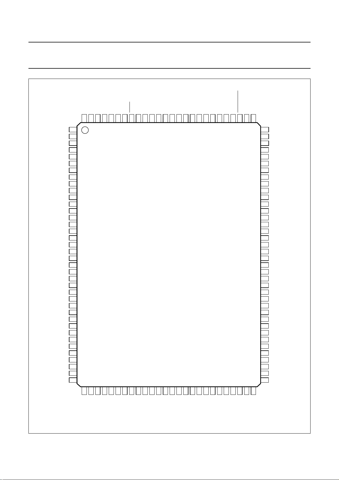
6 PINNING
The SAA7134HL is packaged in a rectangular LQFP (low
profile quad flat package) with 128 pins (see Fig.3).
In Section 6.1 all the pins are sorted by number.
The pin description for the functional groups is given in
Tables 2 to 7:
• Power supply pins
• PCI interface pins
• Analog interface pins
• Joint Test Action Group (JTAG) test interface pins for
boundary scan test
• I2C-bus multi-master interface
• General purpose interface (pins GPIO) and the main
functions.
The characteristicsof the pintypes are detailedin Table 8.
6.1 Pins sorted by number SYMBOL PIN
V
DDD
1
GNT# 2
REQ# 3
AD[31] 4
AD[30] 5
AD[29] 6
AD[28] 7
AD[27] 8
AD[26] 9
AD[25] 10
AD[24] 11
C/BE[3]# 12
IDSEL 13
AD[23] 14
AD[22] 15
AD[21] 16
AD[20] 17
AD[19] 18
V
V
DDD
SSD
19
20
AD[18] 21
AD[17] 22
AD[16] 23
C/BE[2]# 24
SYMBOL PIN
FRAME# 25
IRDY# 26
TRDY# 27
DEVSEL# 28
STOP# 29
PERR# 30
SERR# 31
PAR 32
C/BE[1]# 33
AD[15] 34
AD[14] 35
AD[13] 36
AD[12] 37
V
V
DDD
SSD
38
39
PCI_CLK 40
AD[11] 41
AD[10] 42
AD[09] 43
AD[08] 44
C/BE[0]# 45
AD[07] 46
AD[06] 47
AD[05] 48
AD[04] 49
AD[03] 50
AD[02] 51
AD[01] 52
AD[00] 53
V
V
DDD
SSD
54
55
GPIO23 56
GPIO22 57
GPIO21 58
GPIO20 59
GPIO19 60
GPIO18 61
XTALI 62
XTALO 63
V
V
SSD
DDD
64
65
2002 Dec 17 8
Page 9
Philips Semiconductors Product specification
PCI audio and video broadcast decoder SAA7134HL
SYMBOL PIN
V_CLK 66
GPIO17 67
GPIO16 68
GPIO15 69
GPIO14 70
GPIO13 71
GPIO12 72
V
V
DDD
SSD
73
74
GPIO11 75
GPIO10 76
GPIO9 77
GPIO8 78
GPIO7 79
GPIO6 80
GPIO5 81
GPIO4 82
GPIO3 83
GPIO2 84
GPIO1 85
GPIO0 86
GPIO27 87
GPIO26 88
GPIO25 89
SCL 90
SDA 91
V
V
DDD
SSD
92
93
LEFT2 94
V
DDA
95
LEFT1 96
V
SSA
97
RIGHT1 98
V
REF0
99
RIGHT2 100
V
V
REF1
REF2
101
102
OUT_RIGHT 103
OUT_LEFT 104
PROP_RST 105
SIF 106
SYMBOL PIN
V
V
REF3
SSA
107
108
CV2_C 109
V
V
DDA
REF4
110
111
DRCV_Y 112
V
SSA
113
CV0_Y 114
V
DDA
115
CV1_Y 116
DRCV_C 117
CV3_C 118
V
SSA
119
CV4 120
TRST 121
TCK 122
TMS 123
TDO 124
TDI 125
INT_A 126
PCI_RST# 127
V
SSD
128
2002 Dec 17 9
Page 10
Philips Semiconductors Product specification
PCI audio and video broadcast decoder SAA7134HL
6.2 Pins grouped by function Table 2 Power supply pins
SYMBOL PIN TYPE DESCRIPTION
V
SSA
97, 108, 113
and 119
V
DDA
95, 110
and 115
V
SSD
20, 39, 55,
64, 74, 93
and 128
V
DDD
1, 19,38, 54,
65, 73
and 92
Table 3 PCI interface pins; note 1
SYMBOL PIN TYPE DESCRIPTION
PCI_CLK 40 PI PCI clock input: reference for all bus transactions, up to 33.33 MHz
PCI_RST# 127 PI PCI reset input: will 3-state all PCI pins (active LOW)
AD[31] to
AD[00]
4 to 11,
14 to 18,
21 to 23,
34 to 37,
41 to 44 and
46 to 53
C/BE[3]# to
C/BE[0]#
12, 24, 33
and 45
PAR 32 PIOand
FRAME# 25 PIOand
TRDY# 27 PIOand
IRDY# 26 PIOand
STOP# 29 PIOand
IDSEL 13 PI initialization device select input: this input is used to select the SAA7134HL
DEVSEL# 28 PIOand
REQ# 3 PO PCI request output: the SAA7134HL requests master access to PCI-bus
GNT# 2 PI PCI grant input: the SAA7134HL is granted to master access PCI-bus
AG analog ground for integrated analog signal processing
AS analog supply voltage for integrated analog signal processing
VG digital ground for digital circuit, core and I/Os
VS digital supply voltage for digital circuit, core and I/Os
PIOand
multiplexed address and data input or output: bi-directional, 3-state
T/S
PIOand
T/S
command code input or output: indicates type of requested transaction and
byte enable, for byte aligned transactions (active LOW)
parity input or output: driven by the data source, even parity over all pins AD
T/S
and C/BE#
frame input or output: driven by the current bus master (owner), to indicate
S/T/S
the beginning and duration of a bus transaction (active LOW)
target ready input or output: driven by the addressed target, to indicate
S/T/S
readiness for requested transaction (active LOW)
initiator ready input or output: driven by the initiator, to indicate readiness to
S/T/S
continue transaction (active LOW)
stop input or output: target is requesting the master to stop the current
S/T/S
transaction (active LOW)
during configuration read and write transactions
device select input or output: driven by the target device, to acknowledge
S/T/S
address decoding (active LOW)
(active LOW)
(active LOW)
2002 Dec 17 10
Page 11

Philips Semiconductors Product specification
PCI audio and video broadcast decoder SAA7134HL
SYMBOL PIN TYPE DESCRIPTION
INT_A 126 PO and
O/D
PERR# 30 PIOand
S/T/S
SERR# 31 PO and
O/D
Note
1. PCI-bus pins are located on the long side of the package to simplify PCI board layout requirements.
Table 4 Analog interface pins; note 1
SYMBOL PIN TYPE DESCRIPTION
XTALI 62 CI quartz oscillator input: 32.11 or 24.576 MHz
XTALO 63 CO quartz oscillator output
LEFT2 94 AI analog audio stereo left 2 input or mono input
V
DDA
95 AS analog supply voltage (3.3V)
LEFT1 96 AI analog audio stereo left 1 input or mono input; default analog pass-through
V
SSA
97 AG analog ground (for audio)
RIGHT1 98 AI analog audio stereo right 1 input or mono input; default analogpass-through
V
REF0
99 AR analog reference ground for audio Sigma Delta ADC; to be connected
RIGHT2 100 AI analog audio stereo right 2 input or mono input
V
V
REF1
REF2
101 AR analog reference voltage for audio Sigma Delta ADC; to be connected
102 AR analog reference voltage for audio Sigma Delta ADC; to be supported with
OUT_RIGHT 103 AO analog audio stereo right channel output; 1 V (RMS) line-out, feeding the
OUT_LEFT 104 AO analog audio stereo left channel output; 1 V (RMS) line-out, feeding the
PROP_RST 105 AO analog output for test and debug purpose (active LOW)
SIF 106 AI sound IF input from TV tuner (4.5 to 9.2 MHz); coupling capacitor of 47 pF
V
V
REF3
SSA
107 AR analog reference voltage for audio FIR-DAC and SCART audio input buffer;
108 AG analog ground
CV2_C 109 AI composite video input (mode 2) or C input (modes 6 and 8)
V
V
DDA
REF4
110 AS analog power supply (3.3 V)
111 AR analog reference voltage; to be supported with a capacitor of 220 nF to
interrupt A output: this pin is an open-drain interrupt output, conditions
assigned by the interrupt register
parity error input or output: the receiving device detects data parity error
(active LOW)
system error output: reports address parity error (active LOW)
to pin OUT_LEFT after reset
to pin OUT_RIGHT after reset
directly to analog ground (V
directly to analog supply voltage (V
pin V
REF0
two parallel capacitors of 47 and 0.1 µF to analog ground (V
SSA
)
) and via a 220 nF capacitor to
DDA
)
SSA
audio loop back cable via a coupling capacitor of 2.2 µF
audio loop back cable via a coupling capacitor of 2.2 µF
after the termination with 50 Ω
to be supported with two parallel capacitors of 47 and 0.1 µF to analog
ground (V
analog ground (V
SSA
)
)
SSA
2002 Dec 17 11
Page 12
Philips Semiconductors Product specification
PCI audio and video broadcast decoder SAA7134HL
SYMBOL PIN TYPE DESCRIPTION
DRCV_Y 112 AR differential reference connection (for CV0 and CV1); to be supported with a
capacitor of 47 nF to analog ground (V
V
SSA
113 AG analog ground
CV0_Y 114 AI composite video input (mode 0) or Y input (modes 6 and 8)
V
DDA
115 AS analog supply voltage (3.3 V)
CV1_Y 116 AI composite video input (mode 1) or Y input (modes 7 and 9)
DRCV_C 117 AR differential reference connection (for CV2, CV3 and CV4); to be supported
with a capacitor of 47 nF to analog ground (V
CV3_C 118 AI composite video input (mode 3) or C input (modes 7 and 9)
V
SSA
119 AG analog ground
CV4 120 AI composite video input (mode 4)
Note
1. The SAA7134HLoffers an interface foranalog video and audiosignals. The relatedanalog supply pins areincluded
in this table.
SSA
)
)
SSA
Table 5 JTAG test interface pins
SYMBOL PIN TYPE DESCRIPTION
TRST 121 I test reset input: drive LOW for normal operating (active LOW)
TCK 122 I test clock input: drive LOW for normal operating
TMS 123 I test mode select input: tie HIGH or let float for normal operating
TDO 124 O test serial data output: 3-state
TDI 125 I test serial data input: tie HIGH or let float for normal operating
Table 6 I
2
C-bus multi-master interface
SYMBOL PIN TYPE DESCRIPTION
SCL 90 IO2 serial clock input (slave mode) or output (multi-master mode)
SDA 91 IO2 serial data input and output; always available
PROP_RST 105 GO propagate reset and D3-hot output; to peripheral board circuitry
2002 Dec 17 12
Page 13

Philips Semiconductors Product specification
PCI audio and video broadcast decoder SAA7134HL
Table 7 GPIO pins and functions; note 1
FUNCTION
SYMBOL PIN TYPE
GPIO27 87 GIO A_SDO (I
GPIO26 88 GIO A_WS (I
GPIO25 89 GIO A_SCK (I
V_CLK 66 GO V_CLK (also gated) − ADC_CLK (out) −
GPIO23 56 GIO HSYNC − ADC_C[0] (LSB) R/W, INT
GPIO22 57 GIO VSYNC TS_LOCK (channel
GPIO21 58 GIO − TS_S_D
GPIO20 59 GIO − TS_CLK (<33 MHz) − R/W
GPIO19 60 GIO − TS_SOP (packet start) − R/W
GPIO18 61 GIO VAUX2 − X_CLK_IN R/W, INT
GPIO17 67 GIO VAUX1 (e.g. VACTIVE) − ADC_Y[0] (LSB) R/W
GPIO16 68 GIO − TS_VAL (valid flag) − R/W, INT
GPIO15 to
GPIO8
69 to 72
and
GIO VP[7:0] for formats:
75 to 78
GPIO7 to
79 to 86 GIO VP extension for 16-bit
GPIO0
AUDIO AND VIDEO
PORT OUTPUTS
2
S-bus data) −−R/W
2
S-bus word
select)
2
S-bus clock) −−R/W
ITU-R BT.656, VMI,
VIP (1.1, 2.0), etc.
formats: ZV, VIP-2,
DMSD, etc.
TS CAPTURE
INPUTS
RAW DTV/DVB
OUTPUTS
GPIO
−−R/W
− R/W, INT
decoder locked)
− R/W
(bit-serial data)
− ADC_Y[8:1] R/W
TS_P_D[7:0]
ADC_C[8:1] R/W
(byte-parallel data)
Note
1. The SAA7134HL offers a peripheral interface with General Purpose Input/Output (GPIO) pins. Dedicated functions
can be selected:
a) Digital Video Port (VP):output only;in 8-bitand 16-bitformats, suchas VMI, DMSD(ITU-R BT.601); zoom-video,
with discrete sync signals; ITU-R BT.656; VIP (1.1 and 2.0), with sync encoded in SAV and EAV codes.
b) Transport Stream (TS) capture input: from the peripheral DTV/DVB channel decoder; synchronized by Start Of
Packet (SOP); in byte-parallel or bit-serial protocol.
c) Digitized raw DTV/DVB samples stream output: from internal ADCs; to feed the peripheral DTV/DVB channel
decoder.
d) GPIO: as default (no other function selected); static (no clock); read and write from or to individually selectable
pins; latching ‘strap’ information at system reset time.
e) Peripheral interrupt (INT) input: enabled by interrupt enable register; routed to PCI interrupt (INT_A).
2002 Dec 17 13
Page 14

Philips Semiconductors Product specification
PCI audio and video broadcast decoder SAA7134HL
6.3 Pin description
Table 8 Characteristics of pin types and remarks
PIN TYPE DESCRIPTION
AG analog ground
AI analog input; video, audio and sound
AO analog output
AR analog reference support pin
AS analog supply voltage (3.3 V)
CI CMOS input; 3.3 V level (not 5 V tolerant)
CO CMOS output; 3.3 V level (not 5 V tolerant)
GI digital input (GPIO); 3.3 V level (5 V tolerant)
GIO digital input/output (GPIO); 3.3 V level (5 V tolerant)
GO digital output (GPIO); 3.3 V level (5 V tolerant)
I JTAG test input
IO2 digital input and output of the I
O JTAG test output
O/D open-drain output (for PCI-bus); multiple clients can drive LOW at the same time, wired-OR,
floating back to 3-state over several clock cycles
PI input according to PCI-bus requirements
PIO input and output according to PCI-bus requirements
PO output according to PCI-bus requirements
S/T/S sustained 3-state (for PCI-bus); previous owner drives HIGH for one clock cycle before leaving
to 3-state
T/S 3-state I/O (for PCI-bus); bi-directional
VG ground for digital supply
VS supply voltage (3.3 V)
With overscore or # this pin or ‘signal’ is active LOW, i.e. the function is ‘true’ if the logic level is LOW
2
C-bus interface; 3.3 and 5 V compatible, auto-adapting
2002 Dec 17 14
Page 15
Philips Semiconductors Product specification
PCI audio and video broadcast decoder SAA7134HL
handbook, full pagewidth
V
DDD
GNT#
REQ#
AD[31]
AD[30]
AD[29]
AD[28]
AD[27]
AD[26]
AD[25]
AD[24]
C/BE[3]#
IDSEL
AD[23]
AD[22]
AD[21]
AD[20]
AD[19]
V
DDD
V
SSD
AD[18]
AD[17]
AD[16]
C/BE[2]#
FRAME#
IRDY#
TRDY#
DEVSEL#
STOP#
PERR#
SERR#
PAR
C/BE[1]#
AD[15]
AD[14]
AD[13]
AD[12]
V
DDD
SSD
PCI_RST#
V
INT_A
TDI
TDO
TMS
TCK
127
128
126
125
124
123
122
1
2
3
4
5
6
7
8
9
10
11
12
13
14
15
16
17
18
19
20
21
22
23
24
25
26
27
28
29
30
31
32
33
34
35
36
37
38
TRST
121
CV4
120
SSA
V
119
CV3_C
118
SAA7134HL
DRCV_C
CV1_Y
117
116
DDA
V
115
CV0_Y
V
114
113
SSA
DRCV_Y
112
REF4
V
111
DDA
V
110
CV2_C
V
109
108
SSAVREF3
SIF
107
106
PROP_RST
OUT_LEFT
OUT_RIGHT
105
104
103
102
101
100
99
98
97
96
95
94
93
92
91
90
89
88
87
86
85
84
83
82
81
80
79
78
77
76
75
74
73
72
71
70
69
68
67
66
65
V
REF2
V
REF1
RIGHT2
V
REF0
RIGHT1
V
SSA
LEFT1
V
DDA
LEFT2
V
SSD
V
DDD
SDA
SCL
GPIO25
GPIO26
GPIO27
GPIO0
GPIO1
GPIO2
GPIO3
GPIO4
GPIO5
GPIO6
GPIO7
GPIO8
GPIO9
GPIO10
GPIO11
V
SSD
V
DDD
GPIO12
GPIO13
GPIO14
GPIO15
GPIO16
GPIO17
V_CLK
V
DDD
40394142434445464748495051525354555657585960616263
SSD
V
AD[11]
PCI_CLK
AD[10]
AD[09]
AD[08]
AD[07]
C/BE[0]#
AD[06]
AD[05]
AD[04]
AD[03]
AD[02]
Fig.3 Pin configuration.
2002 Dec 17 15
AD[01]
AD[00]
DDD
V
SSD
V
GPIO23
GPIO22
GPIO21
GPIO20
GPIO19
GPIO18
XTALI
XTALO
64
SSD
V
MHB989
Page 16
Philips Semiconductors Product specification
PCI audio and video broadcast decoder SAA7134HL
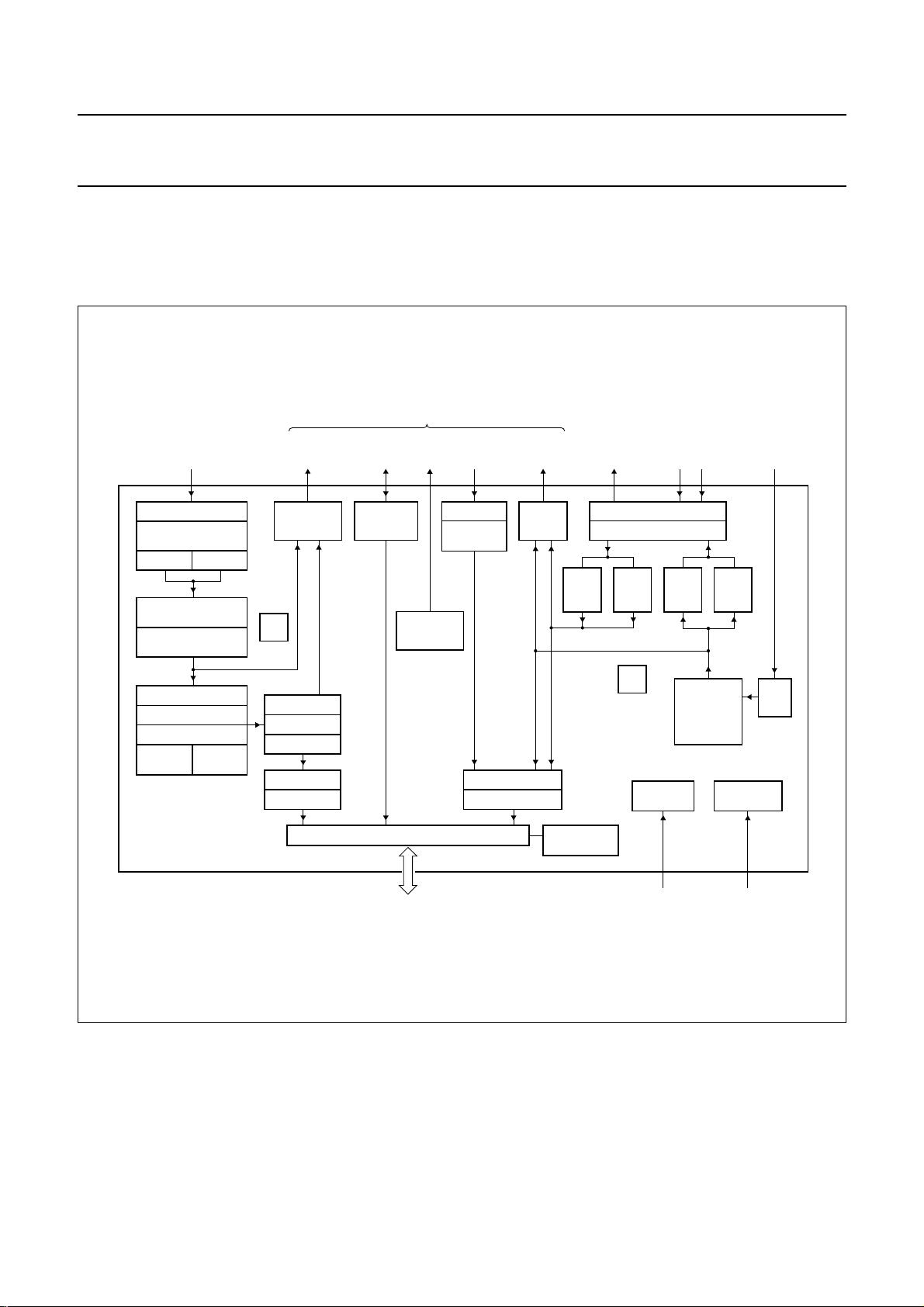
7 FUNCTIONAL DESCRIPTION
7.1 Overview of internal functions
The SAA7134HL is able to capture TV signals over the PCI-bus in personal computers by a single chip (see Fig.4).
handbook, full pagewidth
INPUT SELECTION
CLAMP AND GAIN
CONTROL
9-BIT ADC 9-BIT ADC
DECODER
(NTSC, PAL, SECAM)
ADAPTIVE
COMB FILTER
VIDEO SCALER
RAW VBI
PROGRAM
SET
5 analog
video
inputs
3-D
PROGRAM
SET
digital
video
output
VIDEO PORT
(DIGITAL)
LLC
MATRIX
GAMMA
FORMAT
VIDEO FIFOS
DMA CONTROL
GPIO
2
reset
C-bus
I
I2C-BUS
INTERFACE
PROPAGATE
RESET
PCI-BUS INTERFACE
transport
stream
input
DTV-TS p/s
I2S-BUS
INPUT
AUDIO FIFOS
DMA CONTROL
digital
audio
output
I2S-BUS
OUTPUT
ACPI POWER
MANAGEMENT
stereo
output
ANALOG AUDIO I/O
PASS-THROUGH (DEFAULT)
AUDIO
16-BIT
ADC
AUDIO
16-BIT
ADC
FLC
SAA7134HL
BOUNDARY
SCAN TEST
stereo
input 1
AUDIO
16-BIT
stereo
input 2
DAC
TV SOUND
STEREO
DECODER
(DUAL FM,
NICAM)
IF sound
input
AUDIO
16-BIT
DAC
OSCILLATOR
SIF
ADC
PCI-bus
Fig.4 Functional block diagram.
2002 Dec 17 16
MHB990
crystaltest
Page 17

Philips Semiconductors Product specification
PCI audio and video broadcast decoder SAA7134HL
The SAA7134HL incorporates two 9-bit video ADCs and
the entire decoding circuitry of any analog TV signal:
NTSC, PAL and SECAM, including non-standard signals,
such as playback from a VCR. The adaptive multi-line
comb filter provides superb picture quality, component
separation, sharpness and high bandwidth. The video
stream can be cropped and scaled to the needs of the
application. Scaling down as well as zooming up is
supported in the horizontal and vertical direction, and an
adaptive filter algorithm prevents aliasing artifacts. With
theacquisition unitof thescaler two different‘tasks’ canbe
defined, e.g.to capturevideo to theCPU for compression,
and write video to the screen from the same video source
but with different resolution, colour format and frame rate.
TheSAA7134HL containsTV sound stereodecoding from
Sound IF (SIF), for NICAM standards and dual carrier
FM systems, as used in European and Asian countries.
Basebandstereo audiosamplingis alsoimplemented, e.g.
for capturing from a camcorder or externally decoded
BTSC. Theaudio samplingrate canbe locked tothe video
frame rate to ensure synchronization (lip-sync) between
the video and audio data flow, e.g. for storage,
compression or time shift viewing applications.
The SAA7134HL incorporatesanalog audio pass-through
and support for the analog audio loop back cable to the
sound card function.
The decoded video streams are fed to the PCI-bus, and
arealso appliedto aperipheralstreaming interface,in ITU,
VIP or VMI format. A possible application extension is
on-board hardware MPEG compression, or other feature
processing. The compresseddata is fed back throughthe
peripheral interface, in parallel or serial format, to be
captured bythe systemmemory throughthe PCI-bus. The
Transport Stream (TS) from a DTV/DVB channel decoder
can be captured through the peripheral interface in the
same way.
Audio, video and transport streams are collected in a
configurable FIFO with a total capacity of 1 kbyte. The
DMA controller monitors the FIFO filling degree and
master-writes the audio and video stream to the
associated DMA channel. The virtual memory address
space (from OS) is translated into physical (bus)
addresses bythe on-chiphardware MemoryManagement
Unit (MMU).
7.2 Application examples
The SAA7134HL enables PC TV capture applications
both on the PC mother board and on PCI add-on
TV capture cards. Figures 5 and 6 illustrate some
examples of add-on card applications.
Figure 5 shows the basicapplication tocapture videofrom
analog TV sources.The proposed tuner types incorporate
theRF tuning function andtheIF downconversion. Usually
the IF downconversion stage also includes a single
channel and analog sound FM demodulator. The Philips
tuner FI1216MK2 is dedicated to the 50 Hz system
B/G standard as used in Europe. The FI1236MK2 is the
comparable type for the 60 Hz system M standard for the
USA.Both typesare suitedfor terrestrialbroadcast andfor
cable reception. The tuner provides composite video and
baseband audioas mono or ‘multiplexed’(mpx) in case of
BTSC. These analog video and sound signals are fed to
the appropriate input pins of the SAA7134HL.
Further analogvideo input signals, CVBSand/or Y-C, can
be connected via the board back-panel, or the separate
front connectors, e.g. from a camcorder. Accompanying
stereo audio signals can also be fed to the SAA7134HL.
Video is digitized and decoded to YUV. TV sound is
digitized and decoded to stereo audio, according to
NICAM or dual FM standards. The digital streams are
pumped via DMA into the PCI memory space.
The SAA7134HL incorporates means for legacy analog
audio signal routing. The on-chip audio DACs convert the
digital decoded stereo signal into analog audio. This
analog audio input signal is fed via an analog audio loop
back cable into the line-in of a legacy sound card.
An external audio signal, that would have otherwise
connected directly to the sound card, is now routed
through the SAA7134HL. This analog pass-through is
enabled as default by a system reset, i.e. without any
driver involvement and before system set-up.
During the power-up procedure, the SAA7134HL will
investigate the on-board EEPROM to load the board
specific system vendor ID and board version ID into the
related places of the PCI configuration space. The board
vendorcan storeother boardspecificdata inthe EEPROM
that is accessible via the I2C-bus.
The application of the SAA7134HL is supported by
reference designs and a set of drivers for the Windows
operatingsystem (Videofor Windowsand WindowsDriver
Model compliant).
2002 Dec 17 17
Page 18

Philips Semiconductors Product specification
PCI audio and video broadcast decoder SAA7134HL
handbook, full pagewidth
TV cable
terrestrial
CVBS
S-video
audio
line-in
or
SOUTH
BRIDGE
TV CAPTURE PCI CARD
TV TUNER AND
IF-PLL
CVBS
DECODER FOR
TV SOUND AND
TV VIDEO
DMA MASTER
INTO PCI
SAA7134HL
2
C-bus
I
SIF
analog
audio
loop back
cable
I2C-BUS EEPROM
SYSTEM
VENDOR ID
NORTH
BRIDGE
PCI-bus:
AGP
LOCAL MEMORY
digital video, digital audio, raw VBI, TS
SOUND
CARD
VGA AND
ISA
SYSTEM
MEMORY
FSB
Fig.5 Basic TV capture, with NICAM or dual FM stereo decoding (Europe).
2002 Dec 17 18
CPU AND
CACHE MEMORY
MHB991
Page 19

Philips Semiconductors Product specification
PCI audio and video broadcast decoder SAA7134HL
handbook, full pagewidth
ATV cable
or terrestrial
and
DVB terrestrial
CVBS
S-video
audio
line-in
TV TUNER
IF
ANALOG IF-PLL
CVBS
HYBRID TV CAPTURE PCI CARD
IF
DIGITAL
IF-PLL
SIF TS
DECODER FOR
TV SOUND AND
TV VIDEO
DMA MASTER
INTO PCI
SAA7134HL
digital video, digital audio, raw VBI, TS
I2C-BUS EEPROM
VENDOR ID
PCI-bus:
CHANNEL
DECODER
analog audio
loop back
2
C-bus
I
SYSTEM
DVB-T
cable
SOUND
CARD
SOUTH
BRIDGE
ISA
SYSTEM
MEMORY
Fig.6 Hybrid TV capture board for digital TV (DVB-T) and analog stereo TV reception.
Figure 6 shows an application extension with a hybrid
TV tuner front-endand digital terrestrialchannel decoding
for DTV-T.
The single-conversion tuner TD1316 provides two
dedicated IF signalsfor theanalog IF-PLL(TDA9886) and
the digital IF-PLL (TDA9889). The CVBS (video) and SIF
(sound) outputsignals of the analogIF-PLL can be routed
to one of the video inputs and the SIF input of the
SAA7134HL for analog TV decoding. On the other hand,
the 2nd IF signal of the digital IF-PLL is fed directly to the
interface of the channel decoder (TDA10045), which
decodes the signal into a digital DVB-T Transport
Stream (TS).
NORTH
BRIDGE
FSB
AGP
VGA AND
LOCAL MEMORY
CPU AND
CACHE MEMORY
MHB992
The SAA7134HL captures this TS via the dedicated
peripheral interface into the configurable internal FIFO for
DMA into the PCI memory space.
The packet structure as decoded by the TDA10045 is
maintained ina well-defined buffer structurein the system
memory, and therefore can easily be sorted
(de-multiplexed) by the CPU for proper MPEG decoding.
The Broadcast Driver Architecture (BDA) for Windows
operating systemssupports this type ofhybrid TV capture
application, sharing one capture board for analog and
digital TV reception.
2002 Dec 17 19
Page 20

Philips Semiconductors Product specification
PCI audio and video broadcast decoder SAA7134HL
7.3 Software support
7.3.1 DEVICE DRIVER
A complex and powerful software packet is provided for
theSAA7134HL. This packetincludesplug-and-play driver
and capture driver installations for all commonly used
32-bit Windows platforms.
All platform related drivers support the following:
• Video preview and capture interfaces
• Audio control and audio capture interfaces
• Custom application interface, that enables the
development ofspecialized applications in cases where
the published Windows Application Program Interface
(API) such as WDM or VfW is not sufficient.
Table 9 Microsoft Operation System (MOS) support
MOS DRIVER SUPPORT
Windows 95 Device access is containedwithin a VxD. The Videofor Windows(VfW) capture driver interfaceis a
16-bit user-mode interface.
Windows NT4 Device access is contained in a kernel-mode driver. The VfW capture driver interface is a 32-bit
user-mode interface.
Windows 98 Device access is contained with a kernel-mode Windows Driver Model (WDM) driver. The capture
driver interface is also kernel-mode WDM.
Windows 2000 The driver is binary-compatible with the Windows 98 driver.
Windows ME The driver is binary-compatible with the Windows 98 driver.
Windows XP The driver is binary-compatible with the Windows 98 driver.
7.3.2 SUPPORTING WDM
The WDM driverfor Windows 98 and Windows 2000 (see
Fig.7) is a kernel-mode driver that implements a Kernel
Streaming (KS) filter with output pins for audio, video
preview, video capture and VBI, together with a crossbar
for input source selection and optional connections for
other on-board devices as child drivers. The WDM driver
is implemented as a stream class mini-driver. It also
exposes the external interfaces to support the user-mode
34API DLL. Custom applications and debug tools will
continue to work without the need to load different drivers.
handbook, full pagewidth
TV TUNER
external video inputs
TV AUDIO
XBAR
audio inputs
transport stream in
Fig.7 WDM capture driver filters.
2002 Dec 17 20
SAA7134HL
CAPTURE
DRIVER
MHB993
audio
video preview
video capture
VBI
Page 21

Philips Semiconductors Product specification
PCI audio and video broadcast decoder SAA7134HL
7.3.3 SUPPORTING VfW
The traditional Video for Windows (VfW) interface is
supported for Windows 9x and for Windows NT4.0 (see
Fig.8). In both cases a 32-bit capture driver based on the
SAA713x user-mode API (34API.DLL) controls the video
functionality and the user-mode audio driver
implementation.
The capture driver supports direct draw surfaces for live
video and is able to capture video in packed data formats
and in planar formats. TV applications such as Intel
intercast and Philips teletext are supported by a private
VBI extension.
In the event that VfW has to be implemented as a 16-bit
interface under Windows 9x, a thunk layer is included for
connecting the16-bit interface tothe 32-bit capturedriver.
Old 16-bitapplications usingVfW arestill supported inthis
way.
VidCap
(WIN 9x)
VidCap32
(WIN NT4.0)
• Capture video to a stream of buffers over VBI
• Capture transportstreams (MPEG data) from achannel
decoder chip (OFDM, VSB, QAM) for supporting digital
TV applications, or from an on-board MPEG encoder
chip that is fed by the video output port of the
SAA7134HL
• Capture raw VBI sample stream to a stream of buffers
over the PCI-bus
• Access to the I2C-bus master for controlling other
peripheral circuits.
The 34API transfers thedevice driverfunctionality through
a proxy interface to the user-mode. The proxy interface
adapts to the different kernel-mode implementations, so
that the common 34API can be used on all Windows
operating systems in the same way.
The SDK for the SAA7134HL contains the detailed
description of all software components such as API
documentation forstreaming, tuner control, dialogues and
direct draw control.
The provided sample code will introduce the user into
working with this interface.
All necessary header and library files are provided.
34Vcap16.DLL
34Vcap32.EXE
VBI extension for
intercast, CC, TXT
34Vcap32.DLL
34API.DLL
34W95.VxD
MHB994
Fig.8 VfW driver structure.
7.3.4 SOFTWARE DEVELOPMENT KIT FOR CUSTOMER
RELATED APPLICATIONS
In addition to the capture driver, an Application
Programmers Interface (API) Dynamic Linked Library
(DLL) provides the whole range of functionality to control
the device(see Fig.9). This classlibrary is builtin c++ and
provides methods to:
• Capture video into a fixed buffer (including clipping)
• Capture audio (baseband stereo input or TV sound
decoded fromdual FM or NICAM) over thePCI-bus into
the memory (for PC-VCR application)
34Vcap.DLL
34API.DLL
34WDM.SYS34W95.VxD 34NT4.SYS
MHB995
Fig.9 User program interface.
2002 Dec 17 21
Page 22

Philips Semiconductors Product specification
PCI audio and video broadcast decoder SAA7134HL
7.4 PCI interface
7.4.1 PCI CONFIGURATION REGISTERS
The PCI interface of the SAA7134HL complies with the
“PCI specification 2.2”
and Advanced Configuration and Power Interface (ACPI)
as required by the
The PCI specification defines a structure of the PCI
configuration spacethat isinvestigated during theboot-up
of the system. The configuration registers (see Table 10)
hold information essential for plug-and-play, to allow
system enumeration and basic device set-up without
dependingon thedevice driver,and supportassociationof
the proper software driver. Some of the configuration
information is hard-wired in the device; some information
is loaded during the system start-up.
Thedevice vendor IDishard codedto11 31H, whichisthe
code for Philips as registered with PCI-SIG.
The device ID is hard coded to 71 34H.
During power-up, initiated by PCI reset, the SAA7134HL
fetches additionalsystem information viathe I2C-bus from
the on-board EEPROM, toload actual board type specific
codes for the system vendor ID, sub-system ID (board
version) and ACPI related parameters into the
configuration registers.
and supports power management
“PC Design Guide 2001”
.
7.4.2 ACPI AND POWER STATES
The
“PCI specification 2.2”
requires support of
“Advanced
Configuration and Power Interface specification 1.0”
(ACPI); more details are defined in the
Management Specification 1.0”
The powermanagement capabilitiesand powerstates are
reported in the extended configuration space. The main
purpose of ACPI and PCI power management is to tailor
the power consumption of the device to the actual needs.
The SAA7134HL supports all four ACPI device power
states (see Table 11).
Thepin PROP_RST ofthe peripheralinterface isswitched
active LOW during the PCI reset procedure, and for the
duration of the D3-hot state. Peripheral devices on board
of the add-on card should use the level of this
signal PROP_RST to switch themselves in any
power-savemode (e.g.disabledevice) andresetto default
settings on the rising edge of signal PROP_RST.
.
“PCI Power
Table 10 PCI configuration registers
FUNCTION
Device vendor ID 00 and 01 11 31 for Philips
Device ID 02 and 03 71 34 for SAA7134HL
Revision ID 08 00 or higher
Class code 09 to 0B 04 80 00 multimedia
Memory address space
required
System (board) vendor ID 2C and 2D loaded from EEPROM
Sub-system
(board version) ID
Note
1. X = don’t care.
REGISTER ADDRESS
(HEX)
10 to 13 XXXXXXXX XXXXXXXX
XXXXXX00 00000000 (b)
2E and 2F loaded from EEPROM
VALUE
(HEX)
REMARK
1 kbyte; note 1
2002 Dec 17 22
Page 23

Philips Semiconductors Product specification
PCI audio and video broadcast decoder SAA7134HL
Table 11 Power management table
POWER STATE DESCRIPTION
D0 Normal operation: all functions accessible and programmable. The default setting after reset and
before driver interaction (D0 un-initialized) switches most of the circuitry of the SAA7134HL into
the power-down mode, effectively such as D3-hot.
D1 First step of reduced power consumption: no functional operation; program registers are not
accessible, but content is maintained. Most of the circuitry of the SAA7134HL is disabled with
exception of the crystal and real-time clock oscillators, so that a quick recovery from D1 to D0 is
possible.
D2 Second step of reduced power consumption: no functional operation; program registers are not
accessible, but content is maintained. All functional circuitry of the SAA7134HL is disabled,
including the crystal and clock oscillators.
D3-hot Lowest power consumption: no functional operation. The content of the programming registers
gets lost and is set to default values when returning to D0.
7.4.3 DMA AND CONFIGURABLE FIFO
The SAA7134HL supports seven DMA channels to
master-write captured active video, audio, raw VBI and
DTV/DVB Transport Streams (TS) into the PCI memory.
Each DMA channel contains inherently the definition of
two buffers, e.g. for odd and even fields in case of
interlaced video, or two alternating buffers to capture
continuous audio stream.
The DMA channelsshare in time and space onecommon
FIFO pool of 256 Dwords (1024 bytes) total. It is freely
configurable how much FIFO capacity can be associated
with which DMA channel. Furthermore, a preferred
minimumburst lengthcan beprogrammed, i.e.the amount
of data to be collected before the request for the PCI-bus
is issued. This means that latency behaviour per DMA
channel can be tailored and optimized for a given
application.
In the event that the FIFO of a certain channel overflows
due to latency conflict on the bus, graceful overflow
recovery is applied. The mount of data that gets lost
becauseit couldnotbe transmitted,ismonitored (counted)
and the PCI-bus address pointer is incremented
accordingly. Thus new data will be written to the correct
memory place, after the latency conflict is resolved.
7.4.4 VIRTUAL AND PHYSICAL ADDRESSING
Most operating systems allocate memory to requesting
applications for DMA as continuous ranges in virtual
address space. The data flow over the PCI-bus points to
physical addresses, usually not continuous and split in
pages of 4 kbytes(Intel architecture, most UNIX systems,
Power PC).
The association betweenthe virtual (logic) address space
and the fragmented physical address space is defined in
page tables (system files); see Fig.10.
TheSAA7134HL incorporateshardware support(MMU) to
translate virtual to physical addresses on the fly, by
investigating the related page table information. This
hardware support reduces the demand for real-time
software interaction and interrupt requests, and therefore
saves system resources.
7.4.5 STATUS AND INTERRUPTS ON PCI-BUS
The SAA7134HL provides a set of status information
aboutinternal signalprocessing, videoandaudio standard
detection, peripheral inputs and outputs (pins GPIO) and
behaviour on the PCI-bus. This status information can be
conditionally enabled toraise an interrupt on thePCI-bus,
e.g. completion of a certain DMA channel or buffer, or
change in a detected TV standard, or the state of
peripheral devices.
The causeof anissued interrupt isreported in a dedicated
register, even if theoriginal condition has changed before
the system was able to investigate the interrupt.
2002 Dec 17 23
Page 24

Philips Semiconductors Product specification
PCI audio and video broadcast decoder SAA7134HL
handbook, full pagewidth
0000FH
00017H
0001FH
physical memory
00000H
00007H
= allocated memory space
= page table
000H
007H
015H
page table
00001000H
00008000H
00009000H
0000A000H
0000D000H
00011000H
00014000H
00016000H
0001E000H
DMA DEFINITIONS
(VIRTUAL ADDRESS SPACE)
real-time streams
FIFO
POOL
DMA
ADDRESS
GENERATION
VIRTUAL
TO
PHYSICAL
ADDRESS
TRANSLATION
PCI
TRANSFER AND
CONTROL
physical address space on PCI
MHB996
Fig.10 MMU implementation (shown bit width indication is valid for 4 kbytes mode).
2002 Dec 17 24
Page 25

Philips Semiconductors Product specification
PCI audio and video broadcast decoder SAA7134HL
7.5 Analog TV standards
Analog TV signals are described in three categories of
standards:
• Basic TV systems: defining frame rate, number of lines
per field, levels of synchronization signals, blanking,
black and white, signal bandwidth and the
RF modulation scheme
• Colour transmission: defining colour coding and
modulation method
• Sound and stereo: defining coding for transmission.
TV signals that are broadcasted usually conform fairly
accurately to the standards. Transmission over the air or
through a cable can distort the signal with noise, echoes,
crosstalk or other disturbances.
Video signals from local consumer equipment, e.g. VCR,
camcorder, camera, game console, or even DVD player,
often do not follow the standard specification very
accurately.
Table 12 Overview of basic TV standards
MAIN
PARAMETERS
RF channel width 6 6 7 7 8 7 8 MHz
Video bandwidth 4.2 4.2 5 5 5.5 6 6 MHz
1st sound carrier 4.5, FM 4.5, FM 5.5, FM 5.5, FM 6.0, FM 6.5, FM 6.5, AM MHz
Field rate 59.94006 50 50 50 50 50 50 Hz
Lines per frame 525 625 625 625 625 625 625 −
Line frequency 15.734 15.625 15.625 15.625 15.625 15.625 15.625 kHz
ITU clocks per line 1716 1728 1728 1728 1728 1728 1728 −
Sync, set-up level −40, 7.5 −40, 7.5 −43, 0 −43, 0 −43, 0 −43, 0 −43, 0 IRE
Gamma correction 2.2 2.2 2.8 2.8 2.8 2.8 2.8 −
Associated colour
TV standards
Associated stereo
TV sound systems
Country examples USA,
M N B G, H I D/K L
NTSC,
PAL
BTSC,
EIAJ, A2
Japan,
Brazil
PAL PAL PAL PAL SECAM,
BTSC dual FM,
A2
Argentina part of
Europe,
Australia
Playback from video tapecannot be expected to maintain
correct timing, especially not during feature mode (fast
forward, etc.).
Tables 12 to 14 list some characteristics of the various
TV standards.
The SAA7134HL decodes all colour TV standards and
non-standard signals as generated by video tape
recorders e.g. automatic video standard detection can be
applied, with preference options for certain standards, or
the decoder can be forced to a dedicated standard.
The SAA7134HL incorporates TV stereo decoding for
NICAM and dual FM sound systems. BTSC and EIAJ are
demodulated to mono-aural sound, but stereo decoding
can be added externally. Baseband stereo audio can be
fed into the device as analog signal, or in digital form in
I2S-bus format.
STANDARD
NICAM NICAM NICAM,
Spain,
Malaysia,
Singapore
UK,
Northern
Europe
China,
Eastern
Europe
SECAM −
PAL
NICAM −
A2
France,
Eastern
Europe
UNIT
−
2002 Dec 17 25
Page 26

Philips Semiconductors Product specification
PCI audio and video broadcast decoder SAA7134HL
Table 13 TV system colour standards
MAIN
PARAMETERS
NTSC M PAL M PAL N
PAL
BGHID
SECAM
LDGHK
PAL 4.4
(60 Hz)
UNIT
Field rate 59.94 59.94 50 50 50 ≈60 Hz
Lines per frame 525 525 625 625 625 525
Chrominance
3.580 3.576 3.582 4.434 4.406 4.250 4.434 MHz
subcarrier
f
to H ratio 227.5 227.25 229.25 283.75 282 272 n.a.
sc
offset (PAL) −−50 50 −−n.a. Hz
f
sc
Alternating phase no yes yes yes −−yes
Country examples USA,
Japan,
Asia-Pacific
Brazil Middleand
South
America
Europe,
Common-
wealth,
China
France,
Eastern Europe,
Africa, Middle East
VCR
transcoding
NTSC-tape
to PAL
Table 14 TV stereo sound standards
MAIN
PARAMETERS
Stereo coding
MONO BTSC EIAJ A2 (DUAL FM) NICAM
− internal carrier (mpx) 2-Carrier Systems (2CS)
scheme
2nd language − mono SAP on
internal FM
ANALOG SYSTEMS DIGITAL CODING
AM FM 2nd FM carrier DQPSK on FM
asalternative
to stereo
as alternative to
stereo
mono on 1st carrier
UNIT
Sound IF 1st 2nd 1st 2nd
M, N 4.5FM 4.5 4.5 4.5 4.724 not used not used MHz
B, G, H 5.5 FM not used not used 5.5 5.742 5.5 5.850 MHz
I 6.0 FM not used not used not used not used 6.0 6.552 MHz
DK (1) 6.5 FM not used not used 6.5 6.742 6.5 5.850 MHz
DK (2) 6.5 FM −−−6.258 −−MHz
DK (3) 6.5 FM −−−5.742 −−MHz
L 6.5 AM not used not used not used not used 6.5 5.850 MHz
De-emphasis 75 75, dBx 50 50 or 75 50 or J17 µs
Audio bandwidth 15 15 15 15 15 kHz
Country examples world-
wide
USA, South
America
Japan part of Europe, Korea part of Europe, China
2002 Dec 17 26
Page 27

Philips Semiconductors Product specification
PCI audio and video broadcast decoder SAA7134HL
7.6 Video processing
7.6.1 ANALOG VIDEO INPUTS
The SAA7134HL provides five analog video input pins:
• Composite videosignals (CVBS), from tuner orexternal
source
• S-video signals (pairs of Y-C), e.g. from camcorder
• DTV/DVB ‘low-IF’ signal, from an appropriate DTV or
combi-tuner.
Analog anti-alias filters are integrated on chip and
therefore, no external filtersare required. The device also
contains automatic clamp and gain control for the video
input signals, to ensure optimum utilization of the ADC
conversion range. The nominal video signal amplitude is
1 V (p-p) and the gain control can adapt deviating signal
levels inthe rangeof +3 dB to −6 dB. Thevideo inputsare
digitized by two ADCs of 9-bit resolution, with a sampling
rate of nominal 27 MHz (the line-locked clock) for analog
video signals.
7.6.2 VIDEO SYNCHRONIZATION AND LINE-LOCKED CLOCK
The SAA7134HL recovers horizontal and vertical
synchronization signals from the selected video input
signal, even under extremely adverse conditions and
signal distortions. Such distortions are ‘noise’, static or
dynamic echoes from broadcast over air, crosstalk from
neighbouring channels or power lines (hum), cable
reflections,time baseerrorsfrom videotapeplay-back and
non-standard signal levels from consumer type video
equipment (e.g. cameras, DVD).
The heart of this TV synchronization system is the
generation of the Line-Locked Clock (LLC) of nominal
27 MHz, as defined by ITU-R BT.601. The LLC ensures
orthogonal sampling, and always provides a regular
pattern of synchronization signals, that is a fixed and well
defined number of clock pulses per line. This is important
for further video processing devices connected to the
peripheral videoport (pins GPIO).It isvery effective torun
under the LLC of 27 MHz, especially for on-board
hardware MPEG encoding devices, since MPEG is
defined on this clock and sampling frequency.
7.6.3 VIDEO DECODING AND AUTOMATIC STANDARD
DETECTION
The SAA7134HL incorporates colour decoding for any
analog TV signal. All colour TV standards and flavours of
NTSC, PAL,SECAM and non-standardsignals (VCR) are
automaticallyrecognized anddecoded intoluminance and
chrominance components, i.e. Y-CB-CR, also known as
YUV.
The video decoder of the SAA7134HL incorporates an
automatic standard detection, that does not only
distinguish between 50 and 60 Hz systems, but also
determines the colour standard of the video input signal.
Various preferences (‘look first’) for automatic standard
detection can be chosen, or a selected standard can be
forced directly.
7.6.4 ADAPTIVE COMB FILTER
The SAA7134HL applies adaptive comb filter techniques
to improve the separation of luminance and chrominance
components in comparisonto the separation by achroma
notch filter, as used in traditional TV colour decoder
technology. The comb filter compares the signals of
neighbouring lines, taking into account the phase shift of
the chroma subcarrier from line to line. For NTSC the
signalfrom threeadjacent linesareinvestigated, andinthe
event of PAL the comb filter taps are spread over four
lines.
Comb filtering achieves higher luminance bandwidth,
resulting in sharper picture anddetailed resolution. Comb
filtering further minimizes colour crosstalk artifacts, which
would otherwise produce erroneous colours on detailed
luminance structures.
The comb filter as implemented in the SAA7134HL is
adaptive in two ways:
• Adaptive to transitions in the picture content
• Adaptive to non-standard signals (e.g. VCR).
The integrated digital delay lines are always exactly
correct, due to the applied unique line-locked sampling
scheme (LLC). Thereforethe comb filter does not needto
be switched off for non-standard signals and remains
operating continuously.
7.6.5 MACROVISION DETECTION
The SAA7134HL detects if the decoded video signal is
copy protected by the Macrovision system. The detection
logic distinguishes the three levels of the copy protection
as defined in rev. 7.01, and are reported as status
information. The decoded video stream is not effected
directly, but application software and Operation System
(OS) has to ensure, that this video stream maintains
tagged as ‘copy protected’, and such video signal would
leave the system onlywith the reinforced copy protection.
Themulti-level Macrovisiondetection onthe videocapture
side supports proper TV re-encoding on the output point,
e.g. by Philips TV encoders SAA712x or SAA7102.
2002 Dec 17 27
Page 28

Philips Semiconductors Product specification
PCI audio and video broadcast decoder SAA7134HL
7.6.6 VIDEO SCALING
The SAA7134HL incorporates a filter and processing unit
to downscaleor upscale thevideo picture inthe horizontal
and vertical dimension, and in frame rate
(see Figs 11 and 12). The phase accuracy of the
re-samplingprocess is1⁄64ofthe originalsample distance.
This is equivalent to a clock jitter of less than 1 ns. The
filter depthof theanti-alias filteradapts to thescaling ratio,
from 10 tapshorizontally forscaling ratiosclose to 1 : 1,to
up to 74 taps for an icon sized video picture.
Most video capture applications will typically require for
downscaling.But somezooming isrequiredfor conversion
of ITU sampling to square pixel (SQP), or to convert the
240 lines of an NTSC field to 288 lines to comply with
CCITT video phone formats.
handbook, full pagewidth
VBI first line
VBI last line
VBI first sample
1st field (odd, FID = 0)
VBI region, raw samples
video region
- cropped
- scaled
sample rate
scaling
The scaling acquisition definition also includes cropping,
frame rate reduction, anddefines theamount ofpixels and
lines to be transported through DMA over the PCI-bus.
Two programming pages are available to enable
re-programmingof thescalerin the‘shadow’ oftherunning
processing, without holding or disturbing the flow of the
video stream. Alternatively, the two programming pages
can be applied to support two video destinations or
applications with different scaler settings, e.g. firstly to
capture video to CPU for compression (storage, video
phone), and secondly to pre-view the picture on the
monitor screen. A separate scaling region is dedicated to
capture raw VBI samples, with a specific sampling rate,
and be written into its own DMA channel.
VBI last sample
VBI DMA
1st buffer (A)
2nd buffer (A)
active video area
2nd field (even, FID = 1)
VBI region, raw samples
video first line
video region
- cropped
- scaled
video last line
The capture acquisition for scaling and DMA has separate programming
parameters for VBI and video region and associated DMA channels.
active video area
video first pixel video last pixel
sample rate
scaling
Fig.11 Scaler processing with DMA interfacing.
2002 Dec 17 28
video DMA (A)
e.g. interlaced
1st buffer (upper field)
2nd buffer (lower field)
MHB997
Page 29

Philips Semiconductors Product specification
PCI audio and video broadcast decoder SAA7134HL
handbook, full pagewidth
1st field (odd, FID = 0)
VBI region, raw samples
video region (A) - cropped
scaling
active video area
2nd field (even, FID = 1)
VBI region, raw samples
video region (A) - cropped
scaling
active video area
3rd field (odd, FID = 0)
VBI region, raw samples
video region (B)
- skipped for field rate reduction
VBI DMA
sample rate
1st buffer (A)
2nd buffer (A)
3rd buffer (B)
4th buffer (B)
sample rate
video DMA (A)
e.g. interlaced
1st buffer (upper field)
2nd buffer (lower field)
sample rate
active video area
task "B" task "A"
VBI region, raw samples
video region - scaled down CIF
active video area
alternating processing task A/B
Twovideocapturetaskscanbe processed in an alternating manner, without
need to reprogram any scaling parameters or DMA definition.
4th field (even, FID = 1)
sample rate
scaling
Fig.12 Scaler task processing with DMA interfacing.
2002 Dec 17 29
video DMA (B)
e.g. single FID
1st buffer
2nd buffer
(next frame)
MHB998
Page 30

Philips Semiconductors Product specification
PCI audio and video broadcast decoder SAA7134HL
7.6.7 VBI DATA
The Vertical Blanking Interval (VBI) is often utilized to
transportdata overanalog video broadcast.Such datacan
closely relateto theactual videostream, or justbe general
data (e.g. news). Some examples for VBI data types are:
• Closed Caption (CC) for the hearing impaired (CC, on
line 21 of first field)
• Intercast data [in US coded in North-American
Broadcast Text System (NABTS) format, in Europe in
World Standard Teletext (WST)], to transmit internet
related services,optionally associated withactual video
program content
• Teletext, transporting news services and broadcast
related information, Electronic Program Guide (EPG),
widely used in Europe (coded in WST format)
• EPG, broadcaster specific program and schedule
information, sometimeswith proprietary coding scheme
(pay service), usually carried on NABTS, WST, Video
Programming Service (VPS), orproprietary data coding
format
• Video Time Codes (VTC) as inserted in camcorders
e.g. use for video editing
• Copy Guard Management System (CGMS) codes, to
indicate copy protected video material, sometimes
combined with format information [Wide Screen
Signalling (WSS)].
Thisinformation iscoded inthe unusedlines ofthe vertical
blanking interval, between the vertical sync pulse and the
active visible video picture. So-called full-field data
transmission is also possible, utilizing all video lines for
data coding.
The SAA7134HL supports capture of VBI data by the
definition of a VBI region to be captured as raw VBI
samples, that will be sliced and decoded by software on
the host CPU. The raw sample stream is taken directly
from theADC and is notprocessed or filteredby the video
decoder. The samplingrate of raw VBI canbe adjusted to
the needs of the data slicing software.
7.6.8 SIGNAL LEVELS AND COLOUR SPACE
Analog TV video signalsare decoded into itscomponents
luminance and colour difference signals (YUV) or in its
digital form Y-CB-CR. ITU-R BT.601 defines 720 pixels
alongthe line(corresponding toa samplingrate of27 MHz
divided by two), and a certain relationship from level to
number range (see Fig.13).
The video components do not use the entire number
range, but leave some margin for overshoots and
intermediate values during processing. For the raw VBI
samples there is no official specification how to code, but
it is common practice to reserve the lower quarter of the
number range for the sync, and to leave some room for
overmodulation beyond the nominal white amplitude (see
Fig.14).
The automatic clamp and gain control at the video input,
together with the automatic chroma gain control of the
SAA7134HL, ensures that the video components stream
at the output comply to the standard levels. Beyond that
additional brightness, contrast,saturation and hue control
can be applied to satisfy special needs of a given
application. The raw VBI samples can be adjusted
independent of the active video.
The SAA7134HL incorporates the YUV-to-RGB matrix
(optional), the RGB-to-YUV matrix and a three channel
look-up table in between (see Fig.15). Under nominal
settings, the RGB space will use the same number range
as definedby theITU andshown in Fig.13afor luminance,
between 16 and 235. As graphic related applications are
based on full-scale RGB, i.e. 0 to 255, the range can be
stretchedby applyingappropriate brightness,contrast and
saturation values. The look-up table supports gamma
correction (freely definable), and allows other non-linear
signal transformation such as black stretching.
The analog TV signal applies a quite strong gamma
pre-compensation (2.2 for NTSC and 2.8 for PAL).
As computer monitors exhibit a gamma (around 2.5), the
difference between gamma pre-compensation and actual
screen gamma has to be corrected, to achieve best
contrast and colour impression.
The SAA7134HL offers a multitude of formats to write
video streams over the PCI-bus: YUV and RGB colour
space, 15-bit, 16-bit, 24-bit and 32-bit representation,
packed and planar formats. For legacy requirements
(VfW) a clipping procedureis implemented,that allowsthe
definition of 8 overlay rectangles. This process can
alternatively be used to associate ‘alpha’ values to the
video pixels.
2002 Dec 17 30
Page 31

Philips Semiconductors Product specification
PCI audio and video broadcast decoder SAA7134HL
+255
+235
+128
+16
0
white
LUMINANCE 100%
black
+255
+240
+212 +212
+128
U-COMPONENT
+44
+16
0
blue 100%
blue 75%
colourless
yellow 75%
yellow 100%
+255
+240
+128
+44
+16
V-COMPONENT
0
red 100%
red 75%
colourless
cyan 75%
cyan 100%
MGC634
a. Y output range. b. U output range (CB). c. V output range (CR).
Fig.13 Nominal digital levels for YUV (Y, CB and CR) in accordance with ITU-R BT.601.
+255
+209
+71
+60
LUMINANCE
SYNC
1
white
black
black shoulder
sync bottom
a. Sources containing 7.5 IRE black
level offset (e.g. NTSC M).
Fig.14 Nominal digital levels for CVBS and raw VBI samples.
2002 Dec 17 31
+255
+199
LUMINANCE
+60
SYNC
1
white
black shoulder = black
sync bottom
b. Sources not containing black
level offset.
MGD700
Page 32

Philips Semiconductors Product specification
PCI audio and video broadcast decoder SAA7134HL
handbook, full pagewidth
Y
YUV
U
RGB
matrix
V
R
to
G
B
three channel non-linear transformation
Fig.15 Colour space conversion and look-up table.
7.6.9 VIDEO PORT, ITU AND VIP CODES
The decodedand/or scaled video streamcan be captured
via PCI-DMA to the system memory,and/or can be made
available locally through the video side port (VP), using
some of the GPIO pins. Two types of applications are
intended:
• Streaming real-time video to a video side port at the
VGA card, e.g. via ribbon cable over the top
• Feeding video stream to a local MPEG compression
deviceon thesame PCIboard, e.g.for timeshift viewing
applications.
The video port of the SAA7134HL supports the following
8 and 16-bit wide YUV video signalling standards
(see Table 7):
• VMI: 8-bit widedata stream, clocked by LLC = 27 MHz,
with discrete sync signals HSYNC, VSYNC and
VACTIVE
• ITU-R BT.656, parallel: 8-bit wide data stream, clocked
by LLC = 27 MHz, synchronization coded in SAV and
EAV codes
• VIP 1.1 and 2.0: 8-bit or 16-bit wide data stream,
clocked by LLC = 27 MHz, synchronization coded in
SAV and EAV codes (with VIP extensions)
• Zoom Video (ZV): 16-bit wide pixel stream, clocked by
LLC/2 = 13.5 MHz, with discrete sync signals HSYNC
and VSYNC
• ITU-R BT.601 direct (DMSD): 16-bit wide pixel stream,
clocked by LLC = 27 MHz, with discrete sync signals
HSYNC, VSYNC/FID and CREF
R
RGB
G
YUV
matrix
B
Y
to
U
V
MHB999
• Raw DTV/DVB samplestream: 9-bit wide data, clocked
with a copy of signal X_CLK_IN.
The VIP standard can transport scaled video and
discontinuous datastream by allowing theinsertion of ‘00’
as marker for emptyclock cycles. For the other videoport
standards, a data valid flag or gated clock can be applied.
7.7 TV sound
7.7.1 TV SOUND STEREO DECODING
TV soundis modulatedon aninternal soundsubcarrier, on
the upper end of the TV RF channel, at 4.5, 5.5, 6.0,
or 6.5 MHz, dependingon theTV system. Themodulation
is usually on FM and for system L on AM (see Table 14).
There are basically three variants how stereo sound is
encoded on analog TV transmission:
• An internal multiplexed carrier for the difference signal
L − R(BTSC uses AMand EIAJuses FM); thisis similar
to FM radio stereo
• A second independent FM carrier in the RF channel
(dual FM), that can carry the difference signal L − R, or
a second language
• A (second) independent FM/QPSK carrier in the
RF channel (NICAM), carrying a digital audio signal,
stereo, or dual language mono.
Some parameters of the used coding scheme are
modulated on an inaudible pilot carrier.
The SAA7134HL incorporates TV sound decoding from
the Sound Intermediate Frequency (SIF) signal. The
analog SIF signal is taken from the tuner, digitized and
digitally FM or AM demodulated. The pilot tone is
2002 Dec 17 32
Page 33

Philips Semiconductors Product specification
PCI audio and video broadcast decoder SAA7134HL
investigated and the signal is properly stereo decoded.
The SAA7134HL supports TV stereo decoding for all
NICAM and dual FM sound systems on-chip. The digital
FM demodulation maintains stable phase accuracy,
resulting into improved channel separation, compared to
traditional analog demodulation. BTSC and EIAJ are
demodulated to mono-aural sound, but stereo decoding
can be added externally.
The SAA7134HL incorporates baseband stereo audio
ADCs, to capture sound signals associated with external
video sources, e.g. camera, camcorder or VCR.
For concurrent capture of audio and video signals, it is
important to maintain synchronization between the two
streams. The spoken word and other soundshould match
thedisplayed picturewithin avideoframe (1/30s ‘lip-sync’).
The SAA7134HL has special means to lock the audio
samplingclock tothe videoframe frequency(FLC), sothat
a certain fix predefined number of audio samples are
associated with each video field. This is especially
important for video editing, compression and recording,
e.g. time shiftviewing. There is no driftbetween the audio
and video streams, not even for longer recording times.
TV sound offers an audio bandwidth of less than 15 kHz,
that is usually sampled and digitized with 32 kHz. NICAM
as digital sound coding has inherently a 32 kHz sample
rate, locked already on the source side to the video rate.
The digital audio stream can be captured through
dedicated DMA into the PCI memory space, or to the
output in I2S-format to further peripheral digital sound
processing, e.g. virtual surround sound, or converted to
analog stereo via integrated audio DACs, to feed analog
audio over the loop back cableto the sound card function.
7.7.2 ANALOG AUDIO PASS-THROUGH AND LOOP BACK
CABLE
Most operating systems are prepared to deal with audio
input at only one single entry point, namely at the sound
card function. Therefore the sound associated with video
has to get routed through the sound card.
The SAA7134HL supports analog audio pass-throughand
the loop back cable on-chip. No external components are
required. The audio signal, that was otherwise connected
to the sound card line-in, e.g. analog sound from a
CD-ROM drive, has to be connected to oneof theinputs of
the SAA7134HL. By default, after a system reset and
without involvement of any driver, this audio signal is
passed through to the analog audio output pins, that will
feed the loop back cable to the sound card line-in
connector. The AV capture driver has to open the default
pass-through and switch in the TV sound signal by will.
7.8 DTV/DVB channel decoding and TS capture
The SAA7134HL is optimum equipped to support the
application extensionto capture digitalTV signals, e.g. for
VSB (ATSC)or DVB (T/C/S).A hybrid TV tunerfor analog
and digital TV broadcast receptionusually providesa DTV
signal on low IF, i.e. downconverted into a frequency
range from0 to 10 MHz. Suchsignals canbe fed toone of
the 5 video inputs of the SAA7134HL for digitizing. The
digital raw DTV is output at the video port, and is sent to
the peripheral channel decoder, e.g. TDA8961 for VSB-8
decoding. The channel decoder provides the sampling
clock via the external clock input pin X_CLK_IN (up to
36 MHzinput clockfrequency), andadjusts thesignal gain
in the tuner or in the video input path in front of the ADC.
Alternatively, the low IF DTV/DVB signal could be fed
directly to the channel decoder, depending on the
capability for digitizing the selected device.
The peripheral channel decoder circuitry decodes the
digital transmission into bits and bytes, apply error
correction etc. and outputs a packed Transport Stream
(TS) accompaniedby aclock and handshakesignals. The
SAA7134HL captures the TS in parallel or serial protocol,
synchronized by Start Of Packet (SOP), and pumps it via
the dedicatedDMA into the PCI memory space. TheDMA
definition supports automatic toggling between two
buffers.
7.9 Control of peripheral devices
2
7.9.1 I
TheSAA7134HL incorporatesan I2C-busmaster toset-up
and control peripheral devices such as tuner, DTV/DVB
channel decoder, audio DSP co-processors, etc. The
I2C-bus interface itselfis controlled from the PCI-buson a
command level, reading and writing byte by byte. The
actual I2C-bus status is reported (status register) and, as
an option, can raise error interrupts on the PCI-bus.
At PCI reset time, the I2C-bus master receives board
specificinformation fromthe on-boardEEPROMto update
the PCI configuration registers.
The I2C-bus interface is multi-master capable and can
assume slaveoperation too. This allowsapplication of the
device in the stand-alone mode, i.e. with the PCI-bus not
connected. Under the slave mode, all internal
programming registers can be reached via the I2C-bus
with exception of the PCI configuration space.
C-BUS MASTER
2002 Dec 17 33
Page 34

Philips Semiconductors Product specification
PCI audio and video broadcast decoder SAA7134HL
7.9.2 PROPAGATE RESET
The PCI system reset and ACPI power management
state D3 is propagated to peripheral devices by the
dedicated pin PROP_RST. This signal is switched to
active LOW by reset and D3, and is only switched HIGH
under control of the device driver ‘bywill’. The intention is
that peripheral devices will use signal PROP_RST as
Chip-Enable (CE). The peripheral devices should enter a
low power consumption state if pin PROP_RST = LOW,
and reset into default setting at the rising edge.
7.9.3 GPIO
The SAA7134HL offers a set of General Purpose
Input/Output (GPIO) pins, to interface to on-board
peripheral circuits. These GPIOsare intendedto takeover
dedicated functions:
• Digital video port output: 8-bit or 16-bit wide (including
raw DTV)
• Digital audio serial output: i.e. I2S-bus output
• Transportstream input:parallelor serial(also applicable
as I2S-bus input)
• Peripheral interrupt input: four GPIO pins of the
SAA7134HL canbe enabled to raisean interrupt on the
PCI-bus. By thismeans, peripheral devices can directly
intercept with the device driver on changed status or
error conditions.
Any GPIO pin that is not used for a dedicated function is
available for directread and write access via the PCI-bus.
Any GPIO pin can be selected individually as input or
output (masked write). By these means, very tailored
interfacing to peripheral devices can be created via the
SAA7134HL capture driver running on Windowsoperating
systems.
At system reset (PCI reset) all GPIO pins will be set to
3-state and input, and the logic level present on theGPIO
pins at that moment will be saved into a special ‘strap’
register. All GPIO pinshave an internal pull-down resistor
(LOW level), but can be strapped externallywith a 4.7 kΩ
resistor to the supply voltage (HIGH level). The device
driver can investigate the strap register for information
about the hardware configuration of a given board.
8 BOUNDARY SCAN TEST
The SAA7134HL hasbuilt-in logic and five dedicatedpins
to support boundary scan testing which allows board
testing without special hardware (nails).
The SAA7134HLfollows the
TestAccess PortandBoundary -ScanArchitecture”
the Joint Test Action Group (JTAG) chaired by Philips.
The 5 special pins are: Test Mode Select (TMS), Test
Clock (TCK), Test Reset (TRST), Test Data Input (TDI)
and Test Data Output (TDO).
The Boundary Scan Test (BST) functions BYPASS,
EXTEST, SAMPLE, CLAMP and IDCODE are all
supported (see Table 15). Details about the JTAG
BST-test can be found in the specification “
1149.1”
Description Language (BSDL) description of the
SAA7134HL is available on request.
8.1 Initialization of boundary scan circuit
The Test Access Port (TAP) controller of an IC should be
in the reset state (TEST_LOGIC_RESET) when the IC is
in the functional mode. This reset state also forces the
instruction register into a functional instruction such as
IDCODE or BYPASS.
To solve the power-up reset, the standard specifies that
the TAP controller will be forced asynchronously to the
TEST_LOGIC_RESET state by setting pin TRST to LOW
level.
8.2 Device identification codes
When the IDCODE instruction is loaded into the BST
instruction register, the identification register will be
connected internallybetween pins TDIand TDO ofthe IC.
The identification register will load a component specific
code during the CAPTURE_DATA_REGISTER state of
the TAP controller and this code can subsequently be
shifted out. At board level, this codecan be used to verify
component manufacturer, type and version number. The
device identification register contains 32 bits, numbered
31 to 0, where bit 31 is the most significant bit (nearest to
TDI) and bit 0 is the least significant bit (nearest to TDO);
see Fig.16.
A device identification register is specified in
1149.1b-1994”
for the specification of the IC manufacturer, the IC part
number andthe IC version number. Itsbiggest advantage
is thepossibility to checkfor the correct ICs mounted after
production and determination ofthe versionnumber ofICs
during field service.
. A file containing the detailed Boundary Scan
. It is a 32-bit register which contains fields
“IEEE Std.1149.1 -Standard
setby
IEEE Std.
“IEEE Std.
2002 Dec 17 34
Page 35

Philips Semiconductors Product specification
PCI audio and video broadcast decoder SAA7134HL
Table 15 BST instructions supported by the SAA7134HL
INSTRUCTION DESCRIPTION
BYPASS This mandatory instructionprovides a minimumlength serial path(1 bit) between pins TDIand TDO
when no test operation of the component is required.
EXTEST This mandatory instruction allows testing of off-chip circuitry and board level interconnections.
SAMPLE This mandatory instruction can be used to take a sample of the inputs during normal operation of
the component. It can also be used to preload data values into the latched outputs of the boundary
scan register.
CLAMP This optional instruction is useful for testing when not all ICs have BST. This instruction addresses
the bypass register while the boundary scan register is in external test mode.
IDCODE Thisoptional instruction will provide information on the components manufacturer, part number and
version number.
handbook, full pagewidth
MSB LSB
31
28 27 12 11 1 0
TDI TDO
0001
4-bit
version
code
000000101010111000100110100
16-bit part number 11-bit manufacturer
identification
1
mandatory
MHC001
Fig.16 32 bits of identification code.
2002 Dec 17 35
Page 36

Philips Semiconductors Product specification
PCI audio and video broadcast decoder SAA7134HL
9 LIMITING VALUES
In accordance with the Absolute Maximum Rating System (IEC 60134); all ground pins connected together and
grounded (0 V); all supply pins connected together.
SYMBOL PARAMETER CONDITIONS MIN. MAX. UNIT
V
V
∆V
V
V
V
T
T
V
DDD
DDA
SS
IA
I(n)
ID
stg
amb
esd
digital supply voltage −0.5 +4.6 V
analog supply voltage −0.5 +4.6 V
voltage difference between pins V
V
SSD
SSA
and
− 100 mV
input voltage at analog inputs −0.5 +4.6 V
input voltage at pins XTALI, SDA and SCL −0.5 V
DDD
+ 0.5 V
input voltage at digital I/O stages outputs in 3-state −0.5 +4.6 V
outputs in 3-state;
3.0V<V
DDD
< 3.6 V
−0.5 +5.5 V
storage temperature −65 +150 °C
ambient temperature 0 70 °C
electrostatic discharge voltage note 1 −250 +200 V
note 2 −3500 +3500 V
Notes
1. Machine model: L = 0.75 µH, C = 200 pF and R = 0 Ω.
2. Human body model: equivalent to discharging a 100 pF capacitor through a 1.5 kΩ resistor.
10 THERMAL CHARACTERISTICS
SYMBOL PARAMETER CONDITIONS VALUE UNIT
R
th(j-a)
thermal resistance from junction to ambient in free air 34.6 K/W
2002 Dec 17 36
Page 37

Philips Semiconductors Product specification
PCI audio and video broadcast decoder SAA7134HL
11 CHARACTERISTICS
V
= 3.0 to 3.6 V; V
DDD
SYMBOL PARAMETER CONDITIONS MIN. TYP. MAX. UNIT
Supplies
V
V
DDD
DDA
digital supply voltage 3.0 3.3 3.6 V
analog supply voltage 3.0 3.3 3.6 V
P power dissipation power state
Crystal oscillator
f
xtal(nom)
∆f
xtal(n)
nominal crystal frequency crystal 1; see Table 16 − 32.11 − MHz
permissible nominal
frequency deviation
f
P
xtal
drive
oscillator frequency range 24 32.11 33 MHz
crystal power level of drive
at pin XTALO
t
j
V
IH(XTALI)
oscillator clock jitter −−±100 ps
HIGH-level input voltage at
pin XTALI
V
IL(XTALI)
LOW-level input voltage at
pin XTALI
PCI-bus inputs and outputs
V
IH
V
IL
I
LIH
HIGH-level input voltage 2 − 5.75 V
LOW-level input voltage −0.5 − +0.8 V
HIGH-level input leakage
current
I
LIL
LOW-level input leakage
current
V
OH
V
OL
C
i
HIGH-level output voltage IO= −2 mA 2.4 −− V
LOW-level output voltage IO= 3 or 6 mA; note 2 −−0.55 V
input capacitance at
pin PCI_CLK 5 − 12 pF
pin IDSEL −−8pF
other input pins −−10 pF
SR
SR
r
f
output rise slew rate 0.4 to 2.4 V; note 3 1 − 5 V/ns
output fall slew rate 2.4 to 0.4 V; note 3 1 − 5 V/ns
= 3.0 to 3.6 V; T
DDA
=25°C; unless otherwise specified.
amb
D0 for typical application − 1.1 − W
D0 after reset − 0.1 − W
D1 − 0.2 − W
D2 − 0.1 − W
D3-hot − 0.02 − W
crystal 2; see Table 16 − 24.576 − MHz
−−±70 × 10
−6
− 0.5 − mW
2 − V
+ 0.3 V
DDD
−0.3 − +0.8 V
VI= 2.7 V; note 1 −−10 µA
VI= 0.5 V; note 1 −−−10 µA
2002 Dec 17 37
Page 38

Philips Semiconductors Product specification
PCI audio and video broadcast decoder SAA7134HL
SYMBOL PARAMETER CONDITIONS MIN. TYP. MAX. UNIT
t
val
t
on
t
off
t
su
t
h
t
rst(CLK)
t
rst(off)
2
C-bus interface, compatible to 3.3 and 5 V signalling (pins SDA and SCL)
I
f
bit
V
IL
V
IH
V
OL
Analog video inputs
CLK to signal valid delay see Fig.17; note 4
bused signals 2 − 11 ns
point-to-point signals 2 − 12 ns
float-to-active delay see Fig.17; note 5 2 −− ns
active-to-float delay see Fig.17; note 5 −−28 ns
input set-up time to CLK see Fig.17; note 4
bused signals 7 −− ns
point-to-point signals 10 (12) −− ns
input hold time from CLK see Fig.17 0 −− ns
reset active time after CLK
note 6 100 −− µs
stable
reset active to output float
notes 5, 6 and 7 −−40 ns
delay
bit frequency rate 0 − 400 kbits/s
LOW-level input voltage note 8 −0.5 − 0.3V
HIGH-level input voltage note 8 0.7V
LOW-level output voltage I
=3mA −−0.4 V
o(sink)
DD(I2C)
− V
DD(I2C)
DD(I2C)
V
+ 0.5 V
INPUTS (PINS CV0 TO CV4)
I
clamp
V
i(p-p)
clamping current DC input voltage VI= 0.9 V −±8−µA
input voltage
note 9 0.375 0.75 1.07 V
(peak-to-peak value)
C
i
input capacitance −−10 pF
9-BIT ANALOG-TO-DIGITAL CONVERTERS
α
cs
channel crosstalk fi< 5 MHz −−−50 dB
B analog bandwidth at −3 dB; ADC only;
note 10
φ
dif
differential phase amplifier plus anti-alias
filter bypassed
G
dif
differential gain amplifier plus anti-alias
filter bypassed
LE
DC(d)
LE
DC(i)
S/N signal-to-noise ratio f
DC differential linearity error − 1.4 − LSB
DC integral linearity error − 2 − LSB
= 4 MHz; anti-alias filter
i
bypassed; AGC = 0 dB
ENOB effective number of bits f
= 4 MHz; anti-alias filter
i
bypassed; AGC = 0 dB
− 7 − MHz
− 2 − deg
− 2 − %
− 50 − dB
− 8 − bit
2002 Dec 17 38
Page 39

Philips Semiconductors Product specification
PCI audio and video broadcast decoder SAA7134HL
SYMBOL PARAMETER CONDITIONS MIN. TYP. MAX. UNIT
Analog sound input (pin SIF)
V
i(max)(p-p)
maximum input voltage
(peak-to-peak value)
V
i(min)(p-p)
minimum input voltage for
lower limit of AGC
(peak-to-peak value)
AGC AGC range of sound input in addition to 0 and −10 dB
f
i
R
i
C
i
input frequency 4 − 9.2 MHz
input resistance default pre-gain selection
input capacitance − 7.5 11 pF
Analog audio inputs (pins LEFT1, RIGHT1, LEFT2 and RIGHT2) and outputs (pins OUT_LEFT and
OUT_RIGHT)
V
i(nom)(rms)
nominal input voltage
(RMS value)
V
i(max)(rms)
maximum input voltage
(RMS value)
V
o(max)(rms)
maximum output voltage
(RMS value)
R
i
R
o
R
L(AC)
C
L
V
offset(DC)
input resistance V
output resistance 150 250 375 Ω
AC load resistance 10 −− kΩ
output load capacitance −−12 nF
static DC offset voltage − 10 30 mV
THD + N total harmonic
distortion-plus-noise
S/N signal-to-noise ratio reference voltage
α
ct
α
cs
crosstalk attenuation between any analog input
channel separation between left and right of
input level adjustment at
− 941 − mV
0dB
input level adjustment at
− 2976 − mV
−10 dB
input level adjustment at
− 59 − mV
0dB
input level adjustment at
− 188 − mV
−10 dB
− 24 − dB
switch
10 −− kΩ
for pin SIF (0 dB)
note 11 − 200 − mV
THD < 3%; note 12 − 12 V
THD<3% − 1 − V
= 1 V (RMS) − 145 − kΩ
i(max)
V
= 2 V (RMS) − 48 − kΩ
i(max)
V
i=Vo
= 1 V (RMS);
− 0.1 0.3 %
fi= 1 kHz; bandwidth
B = 20 Hz to 20 kHz
70 75 − dB
V
= 1 V (RMS);fi= 1 kHz;
o
“ITU-R BS.468”
weighted;
quasi peak
60 −− dB
pairs; fi= 1 kHz
60 −− dB
each input pair
2002 Dec 17 39
Page 40

Philips Semiconductors Product specification
PCI audio and video broadcast decoder SAA7134HL
SYMBOL PARAMETER CONDITIONS MIN. TYP. MAX. UNIT
Sound demodulator performance; note 13
V
o(nom)(rms)
nominal output voltage
(RMS value)
∆f
∆f
FM
FM(FS)
FM deviation B/G standard; THD < 1% ±100 −− kHz
FM deviation at full-scale
level
∆f
FM(max)
maximum FM deviation in
high deviation mode
C/N
C/N
FM
N
FM carrier-to-noise ratio bandwidth NFM= 6 MHz;
NICAM carrier-to-noise
ratio
THD + N total harmonic
distortion-plus-noise
S/N signal-to-noise ratio
B
G
−3dB
resp
−3 dB bandwidth from FM source to any
frequency response from
20 Hz to 14 kHz
α
cs(dual)
dual signal channel
separation
α
cs(stereo)
stereo channel separation note 16 40 45 − dB
note 11 − 280 − mV
terrestrial FM;
±150 −− kHz
level adjustment at 0 dB;
demodulator filter
bandwidth set to narrow
B/G standard; THD < 1%;
±335 −− kHz
demodulator filter
bandwidth set to extra wide
− 77 − dB/Hz
white noise for
S/N = 40 dB;
“ITU-R BS.468”
;
quasi peak
bandwidth NN= 6 MHz;
− 66 − dB/Hz
BER = 10−3; white noise
from FM source to any
output; f
= 1 kHz;
i
− 0.3 0.5 %
B = 20 Hz to 20 kHz
from NICAM source to any
output; V
= 1 V (RMS);
o
− 0.1 0.3 %
fi= 1 kHz;
B = 20 Hz to 20 kHz
“ITU-R BS.468”
;
quasi peak
SC1 from FM source to
64 70 − dB
any output
SC2 from FM source to
60 66 − dB
any output
NICAM source; note 14 −−− dB
14.5 15 − kHz
output
from NICAM source to any
14.5 15 − kHz
output
from FM or NICAM to any
−±2− dB
output; reference
f = 1 kHz, inclusive
pre-emphasis and
de-emphasis
note 15 65 70 − dB
2002 Dec 17 40
Page 41

Philips Semiconductors Product specification
PCI audio and video broadcast decoder SAA7134HL
SYMBOL PARAMETER CONDITIONS MIN. TYP. MAX. UNIT
α
AM
dm
AM
IDENTIFICATION FOR FM SYSTEMS
m
pilot
C/N
pilot
t
ident(on)
t
ident(off)
All digital I/Os: GPIO pins and BST test pins (5 V tolerant)
AM suppression for FM FM with 30% AM (1 kHz)
50 −− dB
modulation; reference
f = 1 kHz and 50 kHz
deviation
AM demodulation SIFlevel is 100 mV (RMS);
36 45 − dB
54% AM; 1 kHz AF;
“ITU-R BS.468”
;
quasi peak
pilot modulation for
25 50 75 %
identification
pilot sideband
− 27 − dB/Hz
carrier-to-noise ratio for
identification start
total identification time on slow mode −−2s
medium mode −−1s
fast mode −−0.5 s
total identification time off slow mode −−2s
medium mode −−1s
fast mode −−0.5 s
P
INS GPIO0 TO GPIO23, V_CLK, GPIO25 TO GPIO27, TDI, TDO, TMS, TCK AND TRST
V
IH
V
IL
I
LI
I
L(I/O)
C
i
R
pd
R
pu
V
OH
V
OL
HIGH-level input voltage 2.0 − 5.5 V
LOW-level input voltage −0.3 − +0.8 V
input leakage current −−1 µA
I/O leakage current 3.3 V signal levels at
V
≥ 3.3 V
DDD
−−10 µA
input capacitance I/O at high-impedance −−8pF
pull-down resistance VI=V
DDD
− 50 − kΩ
pull-up resistance VI=0 − 50 − kΩ
HIGH-level output voltage IO= −2 mA 2.4 − V
+ 0.5 V
DDD
LOW-level output voltage IO= 2 mA 0 − 0.4 V
Audio-video port outputs (digital video stream from comb filter decoder or scaler, digital audio from sound
2
decoder or baseband audio inputs via I
S-bus)
LLC AND LLC2 CLOCK OUTPUT ON PIN V_CLK (see Fig.18)
C
L
T
cy
load capacitance 15 − 50 pF
cycle time LLC active 35 − 39 ns
LLC2 active 70 − 78 ns
δ duty factor CL= 40 pF; note 17
LCC active 35 − 65 %
LCC2 active 35 − 65 %
t
r
rise time 0.4 to 2.4 V −−5ns
2002 Dec 17 41
Page 42

Philips Semiconductors Product specification
PCI audio and video broadcast decoder SAA7134HL
SYMBOL PARAMETER CONDITIONS MIN. TYP. MAX. UNIT
t
f
VIDEO DATA OUTPUT WITH RESPECT TO SIGNAL V_CLK ON PINS GPIO0 TO GPIO17, GPIO22 AND GPIO23 (see Fig.18)
C
L
t
h
t
PD
Raw DTV/DVB outputs (reuse of video ADCs in DVB/TV applications with TDA8960 and TDA8961 for VSB
reception)
CLOCK INPUT SIGNAL X_CLK_IN ON PIN GPIO18
T
cy
δ duty factor note 17 40 50 60 %
t
r
t
f
CLOCK OUTPUT SIGNAL ADC_CLK ON PIN V_CLK
C
L
T
cy
δ duty factor C
t
r
t
f
VSB DATA OUTPUT SIGNALS WITH RESPECT TO SIGNAL ADC_CLK
C
L
t
h
t
PD
TS capture inputs with parallel transport streaming (TS-P); e.g. DVB applications
fall time 2.4 to 0.4 V −−5ns
load capacitance 15 − 50 pF
data hold time notes 18 and 19
LLC active 5 −− ns
LLC2 active 15 −− ns
propagation delay from
positive edge of
signal V_CLK
notes 18 and 19
LLC active −−28 ns
LLC2 active −−55 ns
cycle time 27.8 37 333 ns
rise time 0.8 to 2.0 V −−5ns
fall time 2.0 to 0.8 V −−5ns
load capacitance −−25 pF
cycle time 27.8 −− ns
= 40 pF; note 17 40 − 60 %
L
rise time 0.4 to 2.4 V −−5ns
fall time 2.4 to 0.4 V −−5ns
load capacitance 25 − 50 pF
data hold time inverted and not delayed;
5 −− ns
note 18
propagation delay from
positive edge of
inverted and not delayed;
notes 18 and 20
−−23 ns
signal ADC_CLK
CLOCK INPUT SIGNAL TS_CLK ON PIN GPIO20 (see Fig.19)
T
cy
cycle time − 333 − ns
δ duty factor note 17 40 − 60 %
t
r
t
f
rise time 0.8 to 2.0 V −−5ns
fall time 2.0 to 0.8 V −−5ns
DATA AND CONTROL INPUT SIGNALS ON TS-P PORT (WITH RESPECT TO SIGNAL TS_CLK) ON PINS GPIO0 TO GPIO7,
GPIO16, GPIO19 AND GPIO22 (see Fig.19)
t
su(D)
t
h(D)
input data set-up time 2 −− ns
input data hold time 5 −− ns
2002 Dec 17 42
Page 43

Philips Semiconductors Product specification
PCI audio and video broadcast decoder SAA7134HL
SYMBOL PARAMETER CONDITIONS MIN. TYP. MAX. UNIT
TS capture inputs with serial transport streaming (TS-S); e.g. DVB applications
CLOCK INPUT SIGNAL TS_CLK ON PIN GPIO20 (see Fig.19)
T
cy
δ duty factor note 17 40 − 60 %
t
r
t
f
DATA AND CONTROL INPUT SIGNALS ON TS-S PORT (WITH RESPECT TO SIGNAL TS_CLK) ON PINS GPIO16, GPIO19,
GPIO21 AND GPIO22 (see Fig.19)
t
su(D)
t
h(D)
Notes
1. Input leakage currents include high-impedance output leakage for all bidirectional buffers with 3-state outputs.
2. Pins without pull-up resistors must have a 3 mA output current. Pins requiring pull-up resistors must have 6 mA;
these are pins FRAME#, TRDY#, IRDY#, DEVSEL#, SERR#, PERR#, INT_A and STOP#.
3. This parameter is to be interpreted as the cumulative edge rate across the specified range, rather than the
instantaneous rate at any point within the transition range.
4. REQ# and GNT# are point-to-point signals and have different output valid delay and input set-up times than bused
signals. GNT# has a set-up time of 10 ns. REQ# has a set-up time of 12 ns.
5. For purposesof active orfloat timing measurements,the high-impedanceor ‘off’ stateis defined tobe when thetotal
current delivered through the device is less than or equal to the leakage current specification.
6. RST is asserted and de-asserted asynchronously with respect to CLK.
7. All output drivers floated asynchronously when RST is active.
8. V
DD(I2C)
9. Nominal analog video input signal is to be terminated by 75 Ω that results in 1 V (p-p) amplitude. This termination
resistor should be split into 18 Ω and 56 Ω, and the dividing tap should feed the video input pin, via a coupling
capacitor of 47 nF, to achieve a control range from −3 dB (attenuation) to +6 dB (amplification) for the internal
automatic gain control. See also the application notes of the SAA7130HL/34HL.
10. See user manuals SAA7130HL/34HL for Anti-Alias Filter (AAF).
11. Definition of levels and level setting:
a) The full-scale level for analog audio signals VFS= 0.8 V (RMS). The nominal level at the digital crossbar switch
is defined at −15 dB (FS).
b) Nominal audio input levels: external, mono, Vi= 280 mV (RMS); −9 dB (FS).
12. The analog audio inputs(pins LEFT1, RIGHT1, LEFT2 and RIGHT2) are supported bytwo input levels: 1 V (RMS)
and 2 V (RMS), selectable independently per stereo input pair, LEFT1, RIGHT1 and LEFT2, RIGHT2.
13. V
DDA
parameters in accordance withsystem A2; NICAMin accordancewith EBUspecification; 1 kΩmeasurement source
resistance for AF inputs; V
gain settings according to note 11; for external components see the application diagram in SAA7130HL and
SAA7134HL application notes; unless otherwise specified.
14. The NICAMvalues arein accordancewith the EBUspecification. Audioperformance is limitedby thedynamic range
of theNICAM 728 system. Due to companding,the quantization noiseis never lowerthan −62 dB with respect tothe
input level.
cycle time 37 −− ns
rise time 0.8 to 2.0 V −−5ns
fall time 2.0 to 0.8 V −−5ns
input data set-up time 2 −− ns
input data hold time 5 −− ns
is the extended pull-up voltage of the I2C-bus (3.3 or 5 V bus).
= 3.3 V; settings in accordance with B/G standard; FM deviation is ±50 kHz; f
= 300 mV (p-p); programming registersAGCOFF = 0 and AGCSLOW = 1; leveland
i(SIF)
= 1 kHz; FM sound
mod
2002 Dec 17 43
Page 44

Philips Semiconductors Product specification
PCI audio and video broadcast decoder SAA7134HL
15. FM source; in dual mode only A (respectively B) signal modulated; measured at B (respectively A) channel output;
Vo= 0.8 V (RMS) of modulated channel.
16. FM source; instereo modeonly L (respectively R) signalmodulated; measuredat R (respectively L) channeloutput;
Vo= 0.8 V (RMS) of modulated channel.
t
17. The definition of the duty factor:
18. The output timing must be measured with the load of a 30 pF capacitor to ground and a 500 Ω resistor to 1.4 V.
19. Signal V_CLK inverted; not delayed (default setup).
20. tPD= 6 ns + 0.6T
ADC_CLK
in ns (T
δ
=
-------T
ADC_CLK
H
cy
= 28 ns).
handbook, full pagewidth
CLK
OUTPUT
DELA Y
3-ST ATE
OUTPUT
t
su
INPUT input valid
Fig.17 PCI I/O timing.
1.5 V
t
val
t
on
2.4 V
0.4 V
1.5 V
t
off
t
h
2.4 V
1.5 V1.5 V
0.4 V
MGG280
2002 Dec 17 44
Page 45

Philips Semiconductors Product specification
PCI audio and video broadcast decoder SAA7134HL
handbook, full pagewidth
video data and
control output
(pins GPIO0 to GPIO
22
GPIO
and GPIO23
clock output
(pin V_CLK)
t
PD
t
H
t
f
t
L
t
r
17,
t
h
)
Fig.18 Data output timing (video data, control outputs and raw DTV/DVB).
2.4 V
0.4 V
2.4 V
1.5 V
0.4 V
MHC002
handbook, full pagewidth
TS data and
control input
(pins GPIO0 to GPIO
16,
GPIO
GPIO19
and GPIO21)
TS_CLK
(pin GPIO20
)
7,
t
su(D)
Fig.19 Data input timing (TS data and control inputs).
2002 Dec 17 45
2.0 V
0.8 V
t
h(D)
2.0 V
1.5 V
0.8 V
t
r
t
f
MHC003
Page 46

Philips Semiconductors Product specification
PCI audio and video broadcast decoder SAA7134HL
Table 16 Specification of crystals and related applications (examples); note 1
CRYSTAL FREQUENCY
STANDARD
Crystal specification
Typical load
capacitance
Maximum series
resonance resistance
Typical motional
capacitance
Maximum parallel
capacitance
Maximum permissible
deviation
Maximum temperature
deviation
External components
Typical load
capacitance at
pin XTALI
Typical load
capacitance at
pin XTALO
Typical capacitance of
LC filter
Typical inductance of
LC filter
32.11 MHz 24.576 MHz
FUNDAMENTAL 3rd HARMONIC FUNDAMENTAL 3rd HARMONIC
1B 1C 1A 2B 2C 2A
20 8 8 20 8 10 pF
30 60 50 30 60 80 Ω
20 13.5 1.5 20 1 1.5 fF
73±1 4.3 7 3.3 3.5 pF
±30 × 10
−6
±30 × 10
±30 × 10−6±30 × 10
−6
−6
±30 × 10
±30 × 10
−6
±30 × 10−6±30 × 10
−6
±30 × 10−6±30 × 10
−6
−6
±50 × 10
±20 × 10
−6
−6
33 10 15 27 5.6 18 pF
33 10 15 27 5.6 18 pF
n.a. n.a. 1 n.a. n.a. 1 nF
n.a. n.a. 4.7 n.a. n.a. 4.7 µH
UNIT
Note
1. For oscillator application, see the application notes of the SAA7130HL/34HL.
2002 Dec 17 46
Page 47

Philips Semiconductors Product specification
PCI audio and video broadcast decoder SAA7134HL
12 PACKAGE OUTLINE
LQFP128: plastic low profile quad flat package; 128 leads; body 14 x 20 x 1.4 mm
c
y
X
A
SOT425-1
102
103
pin 1 index
128
1
w M
b
e
p
D
H
D
0 5 10 mm
DIMENSIONS (mm are the original dimensions)
mm
A
max.
1.6
0.15
0.05
1.45
1.35
0.25
0.27
0.17
0.20
0.09
UNIT A1A2A3bpcE
(1)
(1) (1)(1)
D
14.1
20.1
13.9
19.9
65
64
Z
E
e
w M
b
p
39
38
Z
D
v M
B
v M
scale
eH
H
D
22.15
0.5
21.85
E
16.15
15.85
LL
E
A
B
0.75
0.45
H
E
p
A
2
A
A
1
(A )
3
θ
L
p
L
detail X
Zywv θ
Z
E
D
0.81
0.120.2 0.11.0
0.59
0.81
0.59
o
7
o
0
Note
1. Plastic or metal protrusions of 0.25 mm maximum per side are not included.
OUTLINE
VERSION
IEC JEDEC EIAJ
REFERENCES
SOT425-1 136E28 MS-026
2002 Dec 17 47
EUROPEAN
PROJECTION
ISSUE DATE
99-12-27
00-01-19
Page 48

Philips Semiconductors Product specification
PCI audio and video broadcast decoder SAA7134HL
13 SOLDERING
13.1 Introduction to soldering surface mount
packages
Thistext givesa very briefinsight toacomplex technology.
A more in-depth account of soldering ICs can be found in
our
“Data Handbook IC26; Integrated Circuit Packages”
(document order number 9398 652 90011).
There is no soldering method that is ideal for all surface
mount IC packages. Wave soldering can still be used for
certainsurface mountICs,but itis notsuitable forfine pitch
SMDs. In these situations reflow soldering is
recommended.
13.2 Reflow soldering
Reflow soldering requires solder paste (a suspension of
fine solder particles, flux and binding agent) to be applied
tothe printed-circuitboard byscreen printing,stencillingor
pressure-syringe dispensing before package placement.
Several methods exist for reflowing; for example,
convection or convection/infrared heating in a conveyor
type oven. Throughput times (preheating, soldering and
cooling) vary between 100 and 200 seconds depending
on heating method.
Typical reflow peak temperatures range from
215 to 250 °C. The top-surface temperature of the
packages should preferable be kept below 220 °C for
thick/large packages, and below 235 °C for small/thin
packages.
13.3 Wave soldering
Conventional single wave soldering is not recommended
forsurface mountdevices(SMDs) orprinted-circuit boards
with a high component density, as solder bridging and
non-wetting can present major problems.
To overcome these problems the double-wave soldering
method was specifically developed.
If wave soldering isused the following conditions must be
observed for optimal results:
• Use a double-wave soldering method comprising a
turbulent wavewith high upward pressurefollowed by a
smooth laminar wave.
• For packages with leads on two sides and a pitch (e):
– larger than or equal to 1.27 mm, the footprint
longitudinal axis is preferred to be parallel to the
transport direction of the printed-circuit board;
– smaller than 1.27 mm, the footprint longitudinal axis
must be parallel to the transport direction of the
printed-circuit board.
The footprint must incorporate solder thieves at the
downstream end.
• Forpackages withleadson foursides, thefootprint must
be placedat a 45° angleto the transport directionof the
printed-circuit board. The footprint must incorporate
solder thieves downstream and at the side corners.
During placementand beforesoldering, thepackage must
be fixed with a droplet of adhesive. The adhesive can be
applied by screen printing, pin transfer or syringe
dispensing. The package can be soldered after the
adhesive is cured.
Typical dwell time is 4 seconds at 250 °C.
A mildly-activated flux will eliminate the need for removal
of corrosive residues in most applications.
13.4 Manual soldering
Fix the component by first soldering two
diagonally-opposite end leads. Use a low voltage(24 V or
less) soldering iron applied to the flat part of the lead.
Contact time must be limited to 10 seconds at up to
300 °C.
When using a dedicated tool, all other leads can be
soldered in one operation within 2 to 5 seconds between
270 and 320 °C.
2002 Dec 17 48
Page 49

Philips Semiconductors Product specification
PCI audio and video broadcast decoder SAA7134HL
13.5 Suitability of surface mount IC packages for wave and reflow soldering methods
PACKAGE
(1)
SOLDERING METHOD
WAVE REFLOW
(2)
BGA, LBGA, LFBGA, SQFP, TFBGA, VFBGA not suitable suitable
DHVQFN, HBCC, HBGA, HLQFP, HSQFP, HSOP, HTQFP,
not suitable
(3)
suitable
HTSSOP, HVQFN, HVSON, SMS
(4)
PLCC
LQFP, QFP, TQFP not recommended
SSOP, TSSOP, VSO not recommended
, SO, SOJ suitable suitable
(4)(5)
suitable
(6)
suitable
Notes
1. Formore detailedinformation onthe BGA packagesrefer tothe
“(LF)BGAApplication Note
”(AN01026); ordera copy
from your Philips Semiconductors sales office.
2. All surface mount (SMD) packages are moisture sensitive. Depending upon the moisture content, the maximum
temperature (with respect to time) and body size of the package, there is a risk that internal or external package
cracks may occur due to vaporizationof the moisture in them (the so called popcorn effect). Fordetails, refer to the
Drypack information in the
“Data Handbook IC26; Integrated Circuit Packages; Section: Packing Methods”
.
3. These packages are not suitable for wave soldering. On versions with the heatsink on the bottom side, the solder
cannot penetrate between the printed-circuit boardand the heatsink. On versions with the heatsink on the top side,
the solder might be deposited on the heatsink surface.
4. If wave soldering is considered, then the package must be placed at a 45° angle to the solder wave direction.
The package footprint must incorporate solder thieves downstream and at the side corners.
5. Wave solderingis suitable forLQFP, TQFP andQFP packages witha pitch (e)larger than 0.8 mm;it is definitelynot
suitable for packages with a pitch (e) equal to or smaller than 0.65 mm.
6. Wave soldering is suitable for SSOP and TSSOP packages with a pitch (e) equal to or larger than 0.65 mm; it is
definitely not suitable for packages with a pitch (e) equal to or smaller than 0.5 mm.
2002 Dec 17 49
Page 50

Philips Semiconductors Product specification
PCI audio and video broadcast decoder SAA7134HL
14 DATA SHEET STATUS
LEVEL
DATA SHEET
STATUS
(1)
PRODUCT
STATUS
(2)(3)
DEFINITION
I Objective data Development This data sheet contains data from the objective specification for product
development. Philips Semiconductors reserves the right to change the
specification in any manner without notice.
II Preliminary data Qualification This data sheet contains data from the preliminary specification.
Supplementary data will be published at a later date. Philips
Semiconductors reserves the right to change the specification without
notice, in order to improve the design and supply the best possible
product.
III Product data Production This data sheet contains data from the product specification. Philips
Semiconductors reserves the right to make changes at any time in order
to improve the design, manufacturing and supply. Relevant changes will
be communicated via a Customer Product/Process Change Notification
(CPCN).
Notes
1. Please consult the most recently issued data sheet before initiating or completing a design.
2. The product status of the device(s) described in this data sheet may have changed since this data sheet was
published. The latest information is available on the Internet at URL http://www.semiconductors.philips.com.
3. For datasheets describingmultiple type numbers,the highest-level product status determinesthe data sheetstatus.
15 DEFINITIONS
16 DISCLAIMERS
Short-form specification The data in a short-form
specification is extracted from a full data sheet with the
same type number and title. For detailed information see
the relevant data sheet or data handbook.
Limiting valuesdefinition Limiting values givenare in
accordance with the Absolute Maximum Rating System
(IEC 60134). Stress above one or more of the limiting
values may cause permanent damage to the device.
These are stress ratings only and operation of the device
atthese orat anyotherconditions abovethose giveninthe
Characteristics sectionsof the specification isnot implied.
Exposure to limiting values for extended periods may
affect device reliability.
Application information Applications that are
described herein for any of these products are for
illustrative purposes only. Philips Semiconductors make
norepresentation orwarrantythat suchapplicationswill be
suitable for the specified use without further testing or
modification.
Life support applications These products are not
designed for use in life support appliances, devices, or
systems where malfunction of these products can
reasonably be expected toresult inpersonal injury.Philips
Semiconductorscustomers usingorselling theseproducts
for use in such applications do so at their own risk and
agree to fully indemnify Philips Semiconductors for any
damages resulting from such application.
Right to make changes Philips Semiconductors
reserves the right to make changes in the products including circuits, standard cells, and/or software described or contained herein in order to improve design
and/or performance.When theproduct isin full production
(status ‘Production’), relevant changes will be
communicated via a Customer Product/Process Change
Notification (CPCN). Philips Semiconductorsassumes no
responsibility or liability for the use of any of these
products, conveys no licence or title under any patent,
copyright, or mask work right to these products, and
makes no representations or warranties that these
products are free from patent, copyright, or mask work
right infringement, unless otherwise specified.
2002 Dec 17 50
Page 51

Philips Semiconductors Product specification
PCI audio and video broadcast decoder SAA7134HL
ICs with MPEG-audio/AC-3 audio functionality
Purchase ofa PhilipsIC withan MPEG-audio and/orAC-3
audio functionality does not convey an implied license
under anypatent rightto usethis ICin anyMPEG-audio or
AC-3 audio application. For more information please
contact thenearest Philips Semiconductors sales officeor
e-mail: licensing.cip@philips.com.
2
17 PURCHASE OF PHILIPS I
Purchase of Philips I2C components conveys a license under the Philips’ I2C patent to use the
components inthe I2C systemprovided the system conforms to the I2C specificationdefined by
Philips. This specification can be ordered using the code 9398 393 40011.
C COMPONENTS
ICs with MPEG-2 functionality Use of this product in
any manner that complies with the MPEG-2 Standard is
expressly prohibited without a license under applicable
patents in the MPEG-2 patent portfolio, which license is
available from MPEG LA, L.L.C., 250 Steele Street, Suite
300, Denver, Colorado 80206.
2002 Dec 17 51
Page 52

Philips Semiconductors – a w orldwide compan y
Contact information
For additional information please visit http://www.semiconductors.philips.com. Fax: +31 40 27 24825
For sales offices addresses send e-mail to: sales.addresses@www.semiconductors.philips.com.
© Koninklijke Philips Electronics N.V. 2002
All rights are reserved. Reproduction in whole or in part is prohibited without the prior written consent of the copyright owner.
The information presented in this document does not form part of anyquotation or contract, is believed to beaccurate and reliable and maybe changed
without notice. No liability will be accepted by the publisher for any consequence of its use. Publication thereof does not convey nor imply any license
under patent- or other industrial or intellectual property rights.
Printed in The Netherlands 753505/02/pp52 Date of release: 2002 Dec 17 Document order number: 9397 750 10357
SCA74
 Loading...