

Page 1

INTEGRATED CIRCUITS
DATA SH EET
SAA7111A
Enhanced Video Input Processor
(EVIP)
Preliminary specification
Supersedes data of 1996 Sep 05
File under Integrated Circuits, IC22
1996 Nov 07
Page 2

Philips Semiconductors Preliminary specification
Enhanced Video Input Processor (EVIP) SAA7111A
CONTENTS
1 FEATURES
2 APPLICATIONS
3 GENERAL DESCRIPTION
4 QUICK REFERENCE DATA
5 ORDERING INFORMATION
6 BLOCK DIAGRAM
7 PINNING
8 FUNCTIONAL DESCRIPTION
8.1 Analog input processing
8.2 Analog control circuits
8.2.1 Clamping
8.2.2 Gain control
8.3 Chrominance processing
8.4 Luminance processing
8.5 RGB matrix
8.6 VBI-data bypass
8.7 VPO-bus (digital outputs)
8.8 Reference signals HREF, VREF and CREF
8.9 Synchronization
8.10 Clock generation circuit
8.11 Power-on reset and CE input
8.12 RTCO output
8.13 The Line-21 text slicer
8.13.1 Suggestions for I2C-bus interface of the display
software reading line-21 data
9 GAIN CHARTS
10 LIMITING VALUES
11 CHARACTERISTICS
12 TIMING DIAGRAMS
13 CLOCK SYSTEM
13.1 Clock generation circuit
13.2 Power-on control
14 OUTPUT FORMATS
15 APPLICATION INFORMATION
16 I2C-BUS DESCRIPTION
16.1 I2C-bus format
16.2 I2C-bus detail
16.2.1 Subaddress 00
16.2.2 Subaddress 02
16.2.3 Subaddress 03
16.2.4 Subaddress 04
16.2.5 Subaddress 05
16.2.6 Subaddress 06
16.2.7 Subaddress 07
16.2.8 Subaddress 08
16.2.9 Subaddress 09
16.2.10 Subaddress 0A
16.2.11 Subaddress 0B
16.2.12 Subaddress 0C
16.2.13 Subaddress 0D
16.2.14 Subaddress 0E
16.2.15 Subaddress 10
16.2.16 Subaddress 11
16.2.17 Subaddress 12
16.2.18 Subaddress 13
16.2.19 Subaddress 15
16.2.20 Subaddress 16
16.2.21 Subaddress 17
16.2.22 Subaddress 1A (read-only register)
16.2.23 Subaddress 1B (read-only register)
16.2.24 Subaddress 1C (read-only register)
16.2.25 Subaddress 1F (read-only register)
17 FILTER CURVES
17.1 Anti-alias filter curve
17.2 TUF-block filter curve
17.3 Luminance filter curves
17.4 Chrominance filter curves
18 I2C-BUS START SET-UP
19 PACKAGE OUTLINES
20 SOLDERING
20.1 Introduction
20.2 Reflow soldering
20.3 Wave soldering
20.3.1 PLCC
20.3.2 QFP
20.3.3 Method (PLCC and QFP)
20.4 Repairing soldered joints
21 DEFINITIONS
22 LIFE SUPPORT APPLICATIONS
23 PURCHASE OF PHILIPS I2C COMPONENTS
1996 Nov 07 2
Page 3

Philips Semiconductors Preliminary specification
Enhanced Video Input Processor (EVIP) SAA7111A
1 FEATURES
• Four analog inputs, internal analog source selectors,
e.g. 4 × CVBS or 2 × Y/C or (1 × Y/C and 2 × CVBS)
• Two analog preprocessing channels
• Fully programmable static gain for the main channels or
automatic gain control for the selected CVBS or Y/C
channel
• Switchable white peak control
• Two built-in analog anti-aliasing filters
• Two 8-bit video CMOS analog-to-digital converters
• On-chip clock generator
• Line-locked system clock frequencies
• Digital PLL for horizontal-sync processing and clock
generation
• Requires only one crystal (24.576 MHz) for all standards
• Horizontal and vertical sync detection
• Automatic detection of 50 and 60 Hz field frequency,
and automatic switching between PAL and NTSC
standards
• Luminance and chrominance signal processing for
PAL BGHI, PAL N, PAL M, NTSC M, NTSC N,
NTSC 4.43, NTSC-Japan and SECAM
• User programmable luminance peaking or aperture
correction
• Cross-colour reduction for NTSC by chrominance comb
filtering
• PAL delay line for correcting PAL phase errors
• Real time status information output (RTCO)
• Brightness Contrast Saturation (BCS) control on-chip
• The YUV (CCIR-601) bus supports a data rate of:
– 864 × f
– 858 × fH= 13.5 MHz for 525 line sources
• Data output streams for 16, 12 or 8-bit width with the
following formats:
– YUV4:1:1 (12-bit)
– YUV4:2:2 (16-bit)
– YUV4:2:2 (CCIR-656) (8-bit)
– RGB (5, 6, 5) (16-bit) with dither
– RGB (8, 8, 8) (24-bit) with special application
• Odd/even field identification by a non interlace CVBS
input signal
• Fix level for RGB output format during horizontal
blanking
= 13.5 MHz for 625 line sources
H
• 720 active samples per line on the YUV bus
• One user programmable general purpose switch on an
output pin
• Built in line-21 text slicer
• A 27 MHz Vertical Blanking Interval (VBI) data bypass
programmable by I
• Power-on control
• Two via I2C-bus switchable outputs for the digitized
CVBS or Y/C input signals AD1 (7 to 0) and AD2 (7 to 0)
• Chip enable function (reset for the clock generator)
• Compatible with memory-based features (line-locked
clock)
• Boundary scan test circuit complies with the
IEEE Std. 1149.1−1990
• I2C-bus controlled (full read-back ability by an external
controller)
• Low power (<0.5 W), low voltage (3.3 V), small package
(LQFP64)
• 5 V compatible I2C-bus voltage
• 5 V tolerant digital I/O ports.
2 APPLICATIONS
• Desktop/Notebook (PCMCIA) video
• Multimedia
• Digital television
• Image processing
• Video phone
• Intercast.
2
C-bus for INTERCAST applications
(ID-Code = 0 F111 02 B)
1996 Nov 07 3
Page 4
Philips Semiconductors Preliminary specification
Enhanced Video Input Processor (EVIP) SAA7111A
3 GENERAL DESCRIPTION
The Enhanced Video Input Processor (EVIP) is a
combination of a two-channel analog preprocessing circuit
including source selection, anti-aliasing filter and ADC, an
automatic clamp and gain control, a Clock Generation
Circuit (CGC), a digital multi-standard decoder
(PAL BGHI, PAL M, PAL N, NTSC M, NTSC-Japan
NTSC N and SECAM),
a brightness/contrast/saturation control circuit, a colour
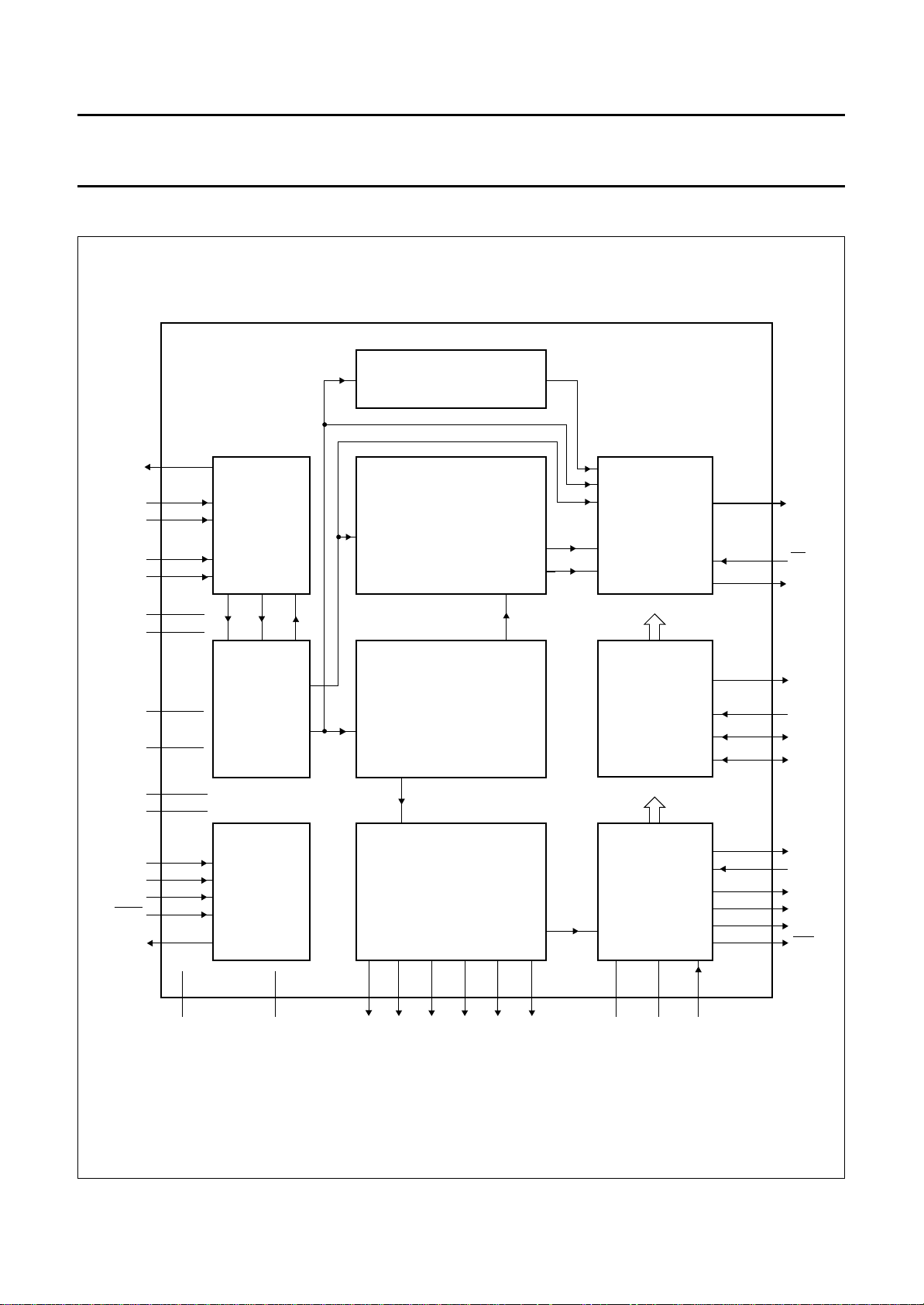
space matrix (see Fig.1) and a 27 MHz VBI-data bypass.
The pure 3.3 V CMOS circuit SAA7111A, analog front-end
and digital video decoder, is a highly integrated circuit for
desktop video applications. The decoder is based on the
principle of line-locked clock decoding and is able to
decode the colour of PAL, SECAM and NTSC signals into
CCIR-601 compatible colour component values. The
SAA7111A accepts as analog inputs CVBS or S-video
(Y/C) from TV or VTR sources. The circuit is I
2
C-bus
controlled.
The SAA7111A then supports several text features as
Line 21 data slicing and a high-speed VBI data bypass for
Intercast.
4 QUICK REFERENCE DATA
SYMBOL PARAMETER MIN. TYP. MAX. UNIT
V
V
T
P
DDD
DDA
amb
A+D
digital supply voltage 3.0 3.3 3.6 V
analog supply voltage 3.1 3.3 3.5 V
operating ambient temperature 0 25 70 °C
analog and digital power − 0.5 − W
5 ORDERING INFORMATION
TYPE
NUMBER
NAME DESCRIPTION VERSION
PACKAGE
SAA7111A LQFP64 plastic low profile quad flat package; 64 leads; body 10 × 10 × 1.4 mm SOT314-2
SAA7111AH QFP64 plastic quad flat package; 64 leads (lead length 1.6 mm); body
SOT393-1
14 × 14 × 2.7 mm
SAA7111AWP PLCC68 plastic leaded chip carrier; 68 leads; body 24 × 24 × 4.5 mm SOT188-2
1996 Nov 07 4
Page 5
Philips Semiconductors Preliminary specification
Enhanced Video Input Processor (EVIP) SAA7111A
6 BLOCK DIAGRAM
handbook, full pagewidth
VBI DATA BYPASS
UPSAMPLING FILTER
BYPASS
AI11
AI12
AI21
AI22
n.c.
SSS
n.c.
TDI
TCK
TMS
TDO
23 (14)
21 (12)
19 (10)
17 (8)
15 (6)
7,8,9 (64)
22 (13)
36,
37
1 (10)
18,14 (9,5)
20,16 (11,7)
12 (3)
2 (59)
13 (4)
1 (58)
11 (2)
ANALOG
PROCESSING
AND
ANALOG-TO-
DIGITAL
CONVERSION
AD2 AD1
ANALOG
PROCESSING
CONTROL
TEST
CONTROL
BLOCK
FOR
BOUNDARY
SCAN TEST
AND
SCAN TEST
CON
CHROMINANCE
C/CVBS
Y/CVBS
BRIGHTNESS
SATURATION
Y
SYNCHRONIZATION
CIRCUIT
AND
CONTRAST
CONTROL
LUMINANCE
CIRCUIT
CIRCUIT
Y
SAA7111A
LFCO
UV
45 to 50
YUV-to-RGB
CONVERSION
AND
OUTPUT
FORMATTER
Y
2
I
C-BUS
CONTROL
2
I
C-BUS
INTERFACE
CLOCKS
CLOCK
GENERATION
CIRCUIT
POWER-ON
CONTROL
53 to 62
(34 to 39)
(42 to 51)
(52) 63
(31) 42
(53) 64
(61) 4
(62) 5
(63) 6
(54) 65
(55) 66
(21) 30
(22) 31
(20) 29
(23) 32
VPO
(0 : 15)
FEI
HREF
GPSW
IICSA
SDA
SCL
XTAL
XTALI
LLC2
CREF
LLC
RES
AOUT
V
V
DDI2C
V
SSA1-2
V
DDA1-2
TRST
(57,41,33,25,18)
68,52,44,34,27
V
DDD1-5
The pin numbers given in parenthesis refer to the 64-pin package.
1996 Nov 07 5
(56,40,32,26,19)
67,51,43,35,28
V
SSD1-5
(30)41(27)38(17)26(29)40(28)39(60)
VREF
RTS0
RTS1
HSVS
3
RTCO
Fig.1 Block diagram.
(15)24(16)25(24)
DDA0
V
SSA0
V
33
MGG061
CE
Page 6
Philips Semiconductors Preliminary specification
Enhanced Video Input Processor (EVIP) SAA7111A
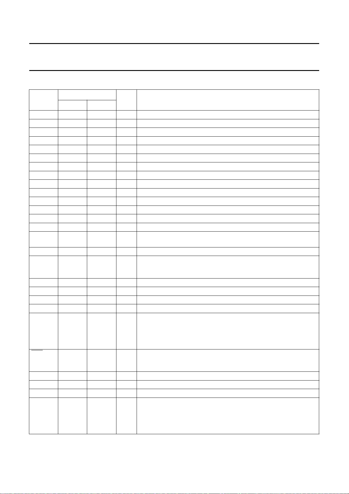
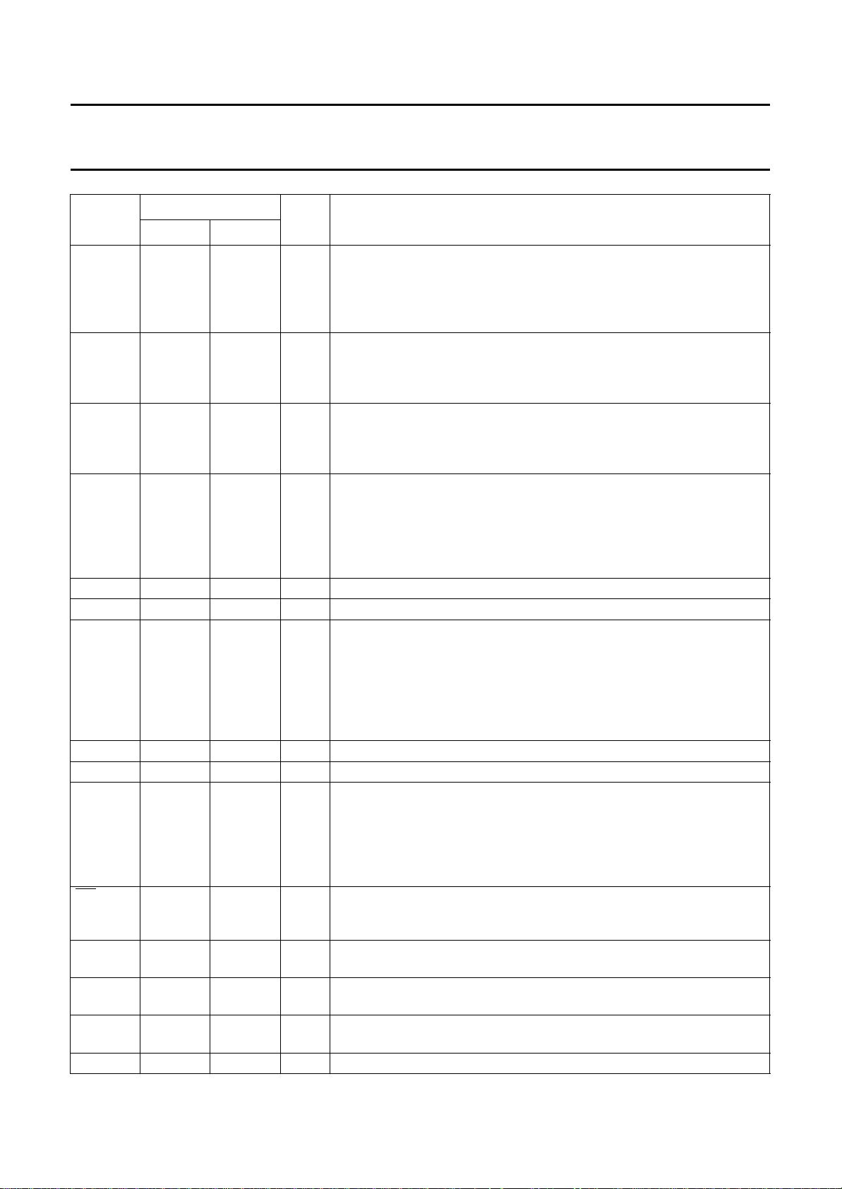
7 PINNING
SYMBOL
I/O/P DESCRIPTION
(L)QFP64 PLCC68
PINS
V
DDI2C
1 10 P open for 3.3 V I2C-bus, connected to 5 V for 5 V I2C-bus compatibility
TDO 2 11 O test data output for boundary scan test; note 3
TDI 3 12 I test data input for boundary scan test; note 3
TMS 4 13 I test mode select input for boundary scan test or scan test; note 3
V
SSA2
5 14 P ground for analog supply voltage channel 2
AI22 6 15 I analog input 22
V
DDA2
7 16 P positive supply voltage for analog channel 2 (+3.3 V)
AI21 8 17 I analog input 21
V
SSA1
9 18 P ground for analog supply voltage channel 1
AI12 10 19 I analog input 12
V
DDA1
11 20 P positive supply voltage for analog channel 1 (+3.3 V)
AI11 12 21 I analog input 11
V
SSS
13 22 P substrate ground connection
AOUT 14 23 O analog test output; for testing the analog input channels
V
DDA0
15 24 P positive supply voltage for internal Clock Generator Circuit (CGC)
(+3.3 V)
V
SSA0
VREF 17 26 O vertical reference output signal (I
16 25 P ground for internal CGC
2
C-bit COMPO = 0) or inverse
composite blanking signal (I2C-bit COMPO = 1) (enabled via I2C-bus
bit OEHV)
V
V
DDD5
SSD5
18 27 P digital supply voltage 5 (+3.3 V)
19 28 P ground for digital supply voltage 5
LLC 20 29 O line-locked system clock output (27 MHz)
1
LLC2 21 30 O line-locked clock
⁄2output (13.5 MHz)
CREF 22 31 O clock reference output: this is a clock qualifier signal distributed by the
internal CGC for a data rate of LLC2. Using CREF all interfaces on the
VPO bus are able to generate a bus timing with identical phase. If
CCIR 656 format is selected (OFTS0 = 1 and OFTS1 = 1) an inverse
composite blanking signal (pixel qualifier) is provided on this pin.
RES 23 32 O reset output (active LOW); sets the device into a defined state. All data
outputs are in high impedance state. The I2C-bus is reset (waiting for
start condition).
CE 24 33 I chip enable; connection to ground forces a reset
V
V
DDD4
SSD4
25 34 P digital supply voltage input 4 (+3.3 V)
26 35 P ground for digital supply voltage input 4
HS 27 38 O horizontal sync output signal (programmable); the positions of the
positive and negative slopes are programmable in 8 LLC increments over
a complete line (= 64 µs) via I
2
C-bus bytes HSB and HSS. Fine position
adjustment in 2 LLC increments can be performed via I2C-bus bits
HDEL1 and HDEL0.
1996 Nov 07 6
Page 7
Philips Semiconductors Preliminary specification
Enhanced Video Input Processor (EVIP) SAA7111A
SYMBOL
I/O/P DESCRIPTION
(L)QFP64 PLCC68
RTS1 28 39 O two functions output; controlled by I2C-bus bit RTSE1.
RTSE1 = 0: PAL line identifier (LOW = PAL line); indicates the inverted
and non-inverted R−Y component for PAL signals. RTSE1 = 1: H-PLL
locked indicator; a high state indicates that the internal horizontal PLL
has locked.
PINS
2
RTS0 29 40 O two functions output; controlled by I
C-bus bit RTSE0.
RTSE0 = 0: odd/even field identification (HIGH = odd field). RTSE0 = 1:
vertical locked indicator; a HIGH state indicates that the internal Vertical
Noise Limiter (VNL) has locked.
2
VS 30 41 O vertical sync signal (enabled via I
C-bus bit OEHV); this signal indicates
the vertical sync with respect to the YUV output. The HIGH period of this
signal is approximately six lines if the VNL function is active. The positive
slope contains the phase information for a deflection controller.
2
HREF 31 42 O horizontal reference output signal (enabled via I
C-bus bit OEHV); this
signal is used to indicate data on the digital YUV bus. The positive slope
marks the beginning of a new active line. The HIGH period of HREF is
720 Y samples long. HREF can be used to synchronize data
multiplexer/demultiplexer. HREF is also present during the vertical
blanking interval.
V
SSD3
V
DDD3
VPO
(15 to 10)
32 43 P ground for digital supply voltage input 3
33 44 P digital supply voltage 3 (+3.3 V)
34 to 39 45 to 50 O digital VPO-bus (Video Port Out) signal; higher bits of the 16-bit VPO-bus
or the 16-bit RGB-bus output signal. The output data rate, the format and
2
multiplexing scheme of the VPO-bus are controlled via I
C-bus bits
OFTS0 and OFTS1. If I2C-bus bit VIPB = 1 the six MSBs of the digitized
input signal are connected to these outputs, configured by the I2C-bus
‘MODE’ bits (see Figs 33 to 40):
LUMA -> VPO15 to VPO8, CHROMA -> VPO7 to VPO0.
V
SSD2
V
DDD2
VPO
(9 to 0)
40 51 P ground for digital supply voltage input 2
41 52 P digital supply voltage 2 (+3.3 V)
42 to 51 53 to 62 O digital VPO-bus output signal; lower bits of the 16-bit YUV-bus or the
16-bit RGB-bus output signal. The output data rate, the format and
2
multiplexing schema of the VPO-bus are controlled via I
C-bus bits
OFTS0 and OFTS1. If I2C-bus bit VIPB = 1 the digitized input signal are
connected to these outputs, configured by the I2C-bus ‘MODE’ bits (see
Figs 33 to 40): LUMA -> VPO15 to VPO8, CHROMA -> VPO7 to VPO0.
FEI 52 63 I fast enable input signal (active LOW); this signal is used to control fast
switching on the digital YUV-bus. A HIGH at this input forces the IC to set
its Y and UV outputs to the high impedance state.
GPSW 53 64 O general purpose switch output; the state of this signal is set via I
2
C-bus
control and the levels are TTL compatible
XT AL 54 65 O second terminal of crystal oscillator; not connected if external clock signal
is used
XTALI 55 66 I input terminal for 24.576 MHz crystal oscillator or connection of external
oscillator with CMOS compatible square wave clock signal
V
SSD1
56 67 P ground for digital supply voltage input 1
1996 Nov 07 7
Page 8
Philips Semiconductors Preliminary specification
Enhanced Video Input Processor (EVIP) SAA7111A
SYMBOL
I/O/P DESCRIPTION
(L)QFP64 PLCC68
PINS
V
DDD1
57 68 P digital supply voltage input 1 (+3.3 V)
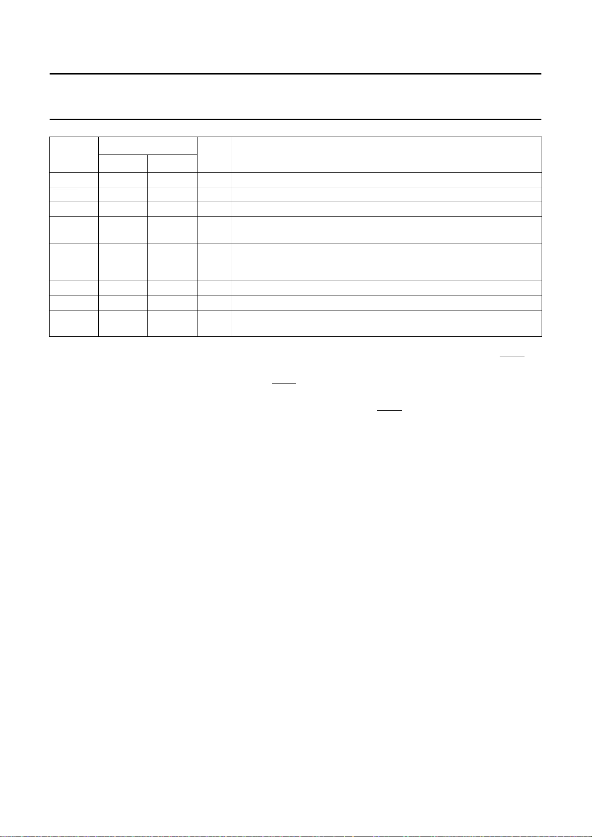
TRST 58 1 I test reset input not (active LOW), for boundary scan test; notes 1, 2, 3
TCK 59 2 I test clock for boundary scan test; note 3
RTCO 60 3 O real time control output: contains information about actual system clock
frequency, subcarrier frequency and phase and PAL sequence
2
IICSA 61 4 I I
C-bus slave address select;
0 = 48H for write, 49H for read
1 = 4AH for write, 4BH for read
2
SDA 62 5 I/O serial data input/output (I
SCL 63 6 I/O serial clock input/output (I
n.c. 64 7, 8, 9,
− not connected
C-bus)
2
C-bus)
36 and 37
Notes
1. For board design without boundary scan implementation (pin compatibility with the SAA7110) connect theTRST pin
to ground.
2. This pin provides easy initialization of BST circuit.TRST can be used to force the TAP (Test Access Port) controller
to the Test-Logic-Reset state (normal operation) at once.
3. In accordance with the
IEEE1149.1
standard the pads TCK, TDI, TMS and TRST are input pads with an internal
pull-up transistor and TDO a 3-state output pad.
1996 Nov 07 8
Page 9
Philips Semiconductors Preliminary specification
Enhanced Video Input Processor (EVIP) SAA7111A
handbook, full pagewidth
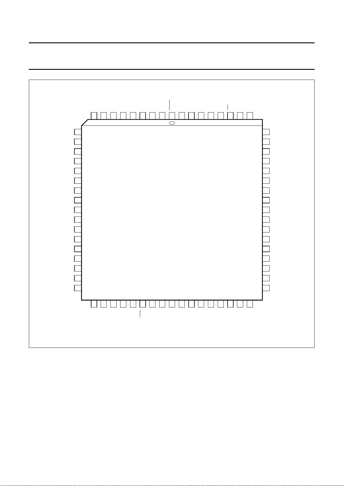
DDD1VSSD1
n.c.
9
n.c.
8
n.c.
7
SCL
6
SDA
5
IICSA
4
RTCO
3
TCK
2
TRST
1
V
68
67
66 XTALI
XTAL
65
GPSW
64
FEI
63
VPO0
62
VPO1
61
V
DDI2C
V
SSA2
V
DDA2
V
SSA1
V
DDA1
V
AOUT
V
DDA0
V
SSA0
VREF
TDO
TDI
TMS
AI22
AI21
AI12
AI11
SSS
10
11
12
13
14
15
16
17
18
19
20
21
22
23
24
25
26
SAA7111A
60
59
58
57
56
55
54
53
52
51
50
49
48
47
46
45
44
VPO3
VPO3
VPO4
VPO5
VPO6
VPO7
VPO8
VPO9
V
DDD2
V
SSD2
VPO10
VPO11
VPO12
VPO13
VPO14
VPO15
V
DDD3
27
28
29LLC
30
31
32
33
34
CE
DDD5
V
SSD5
V
LLC2
CREF
RES
DDD4
V
Fig.2 Pin configuration (PLCC68).
1996 Nov 07 9
35
SSD4
V
36
n.c.
37
n.c.
38
HS
39
RTS1
40
RTS0
41
VS
42
HREF
43
SSD3
V
MGG059
Page 10
Philips Semiconductors Preliminary specification
Enhanced Video Input Processor (EVIP) SAA7111A
handbook, full pagewidth
SSD1
DDD1
TRST
V
58
57
SAA7111A
23
24
CE
RES
V
56
25
DDD4
V
XTALI
55
26
SSD4
V
XTAL
54
27
HS
GPSW
53
28
RTS1
FEI
52
29
RTS0
VPO0
51
30
VS
VPO1
50
31
HREF
VPO2
49
32
SSD3
V
48
47
46
45
44
43
42
41
40
39
38
37
36
35
34
33
VPO3
VPO4
VPO5
VPO6
VPO7
VPO8
VPO9
V
DDD2
V
SSD2
VPO10
VPO11
VPO12
VPO13
VPO14
VPO15
V
DDD3
MGG060
V
DDI2C
V
SSA2
V
DDA2
V
SSA1
V
DDA1
V
AOUT
V
DDA0
V
SSA0
TDO
TDI
TMS
AI22
AI21
AI12
AI11
SSS
RTCO
60
21
LLC2
TCK
59
22
CREF
IICSA
SDA
SCL
n.c.
64
63
62
61
1
2
3
4
5
6
7
8
9
10
11
12
13
14
15
16
17
18
19
20
LLC
DDD5
V
SSD5
V
VREF
1996 Nov 07 10
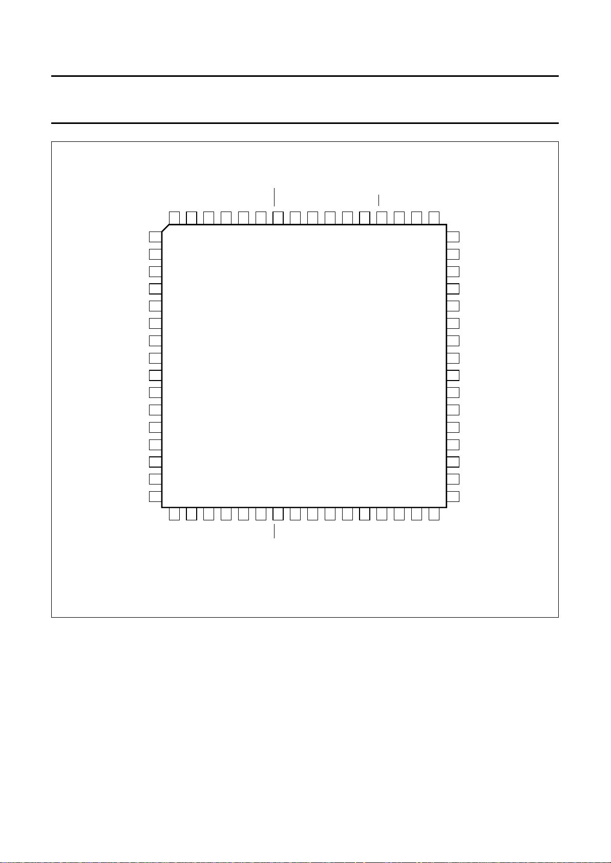
Fig.3 Pin configuration (LQFP64/QFP64).
Page 11
Philips Semiconductors Preliminary specification
Enhanced Video Input Processor (EVIP) SAA7111A
8 FUNCTIONAL DESCRIPTION
8.1 Analog input processing
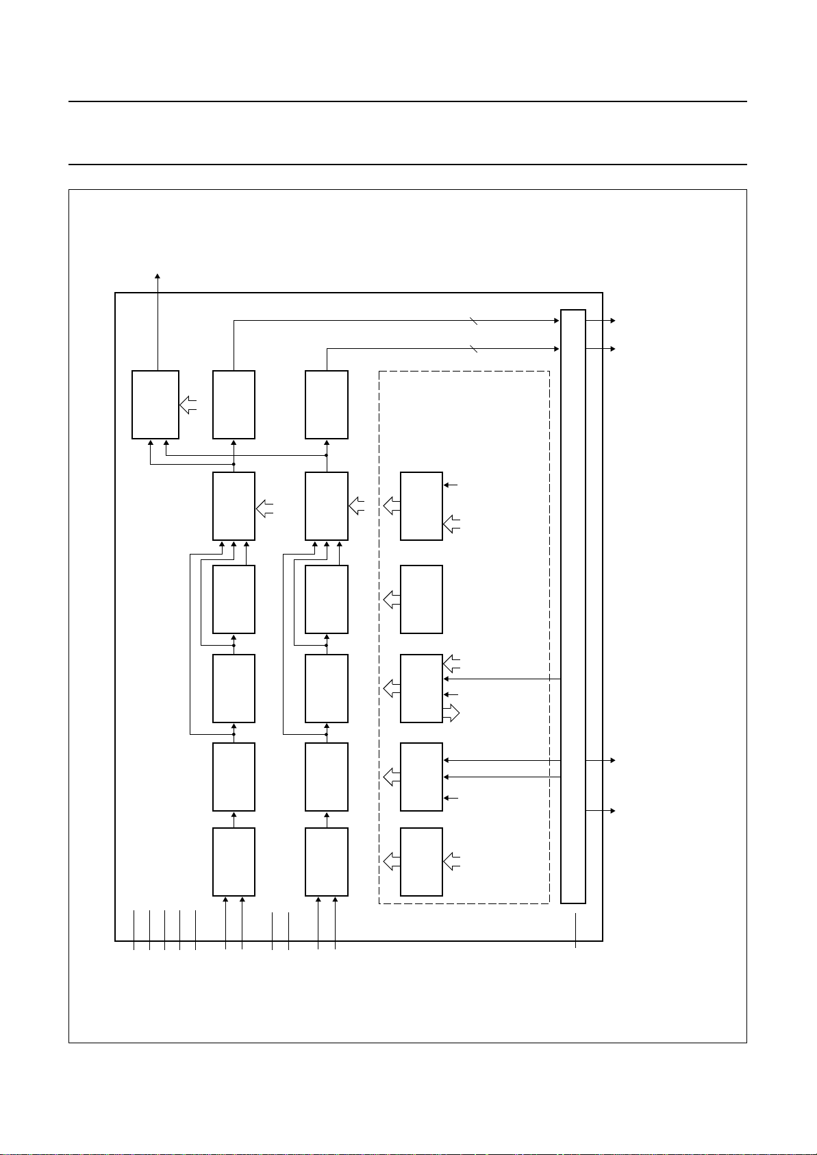
The SAA7111A offers four analog signal inputs, two
analog main channels with source switch, clamp circuit,
analog amplifier, anti-alias filter and video CMOS ADC
(see Fig.9).
8.2 Analog control circuits
The anti-alias filters are adapted to the line-locked clock
frequency via a filter control circuit. During the vertical
blanking time, gain and clamping control are frozen.
8.2.1 C
LAMPING
The clamp control circuit controls the correct clamping of
the analog input signals. The coupling capacitor is also
used to store and filter the clamping voltage. An internal
digital clamp comparator generates the information with
respect to clamp-up or clamp-down. The clamping levels
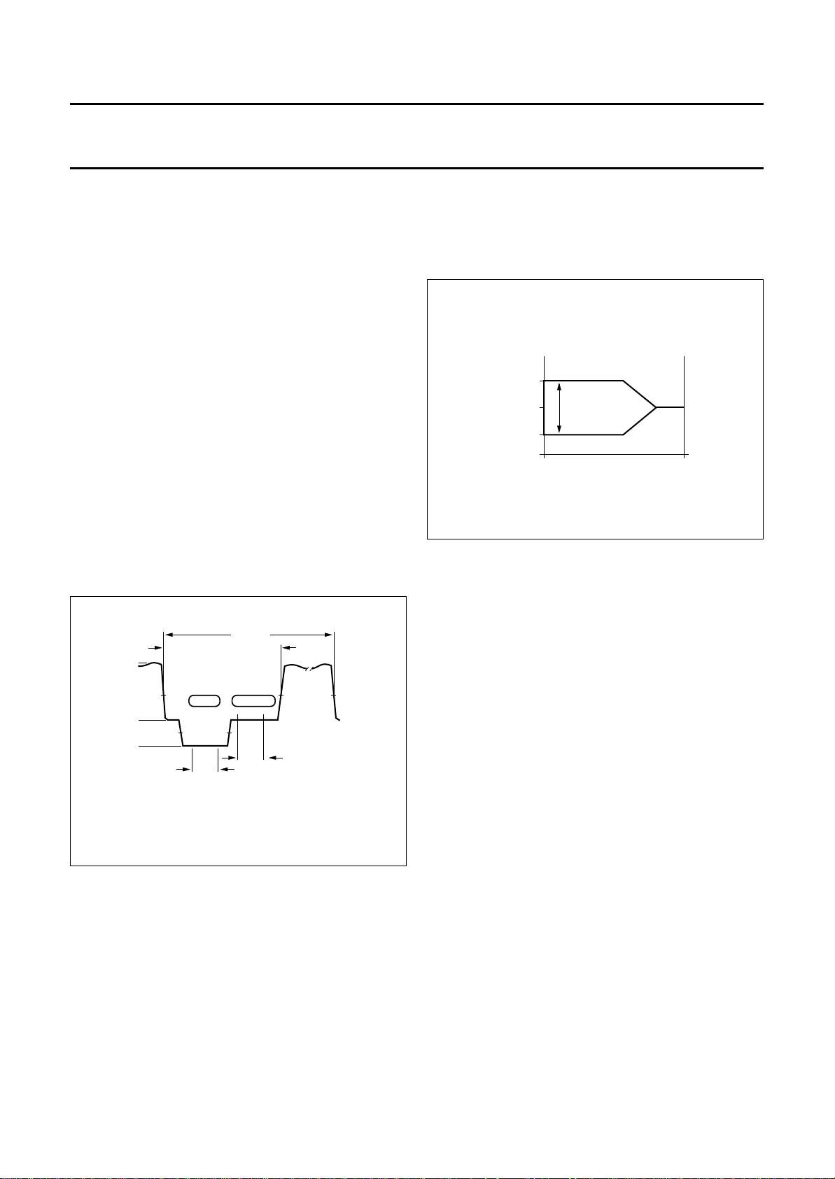
for the two ADC channels are fixed for luminance (60) and
chrominance (128). Clamping time in normal use is set
with the HCL pulse at the back porch of the video signal.
HSY
TV line
HCL
MGC661
handbook, halfpage
225
60
1
analog line blanking
GAIN CLAMP
Fig.4 Analog line with clamp (HCL) and gain
range (HSY).
8.2.2 G
AIN CONTROL
Signal (white) peak control limits the gain at signal
overshoots. The flow charts (see Figs 13 and 14) show
more details of the AGC. The influence of supply voltage
variation within the specified range is automatically
eliminated by clamp and automatic gain control.
The AGC (automatic gain control for luminance) is used to
amplify a CVBS or Y signal to the required signal
amplitude, matched to the ADCs input voltage range.
The AGC active time is the sync bottom of the video signal.
handbook, halfpage
(1 V(p-p) 27/47 Ω)
analog input level
+4.5 dB
−7.5 dB
maximum
minimum
range tbf0 dB
controlled
ADC input level
0 dB
MGG063
Fig.5 Automatic gain range.
8.3 Chrominance processing
The 8-bit chrominance signal is fed to the multiplication
inputs of a quadrature demodulator, where two subcarrier
signals from the local oscillator DTO1 are applied
(0 and 90° phase relationship to the demodulator axis).
The frequency is dependent on the present colour
standard. The output signals of the multipliers are
low-pass filtered (four programmable characteristics) to
achieve the desired bandwidth for the colour difference
signals (PAL, NTSC) or the 0 and 90° FM-signals
(SECAM).
The colour difference signals are fed to the
Brightness/Contrast/Saturation block (BCS), which
includes the following five functions:
• AGC (Automatic Gain Control for chrominance PAL and
NTSC)
• Chrominance amplitude matching (different gain factors
for R−Y and B−Y to achieve CCIR-601 levels Cr and Cb
for all standards)
• Chrominance saturation control
• Luminance contrast and brightness.
• Limiting YUV to the values 1 (min.) and 254 (max.) to
fulfil CCIR-601 requirements.
The gain control circuit receives (via the I2C-bus) the static
gain levels for the two analog amplifiers or controls one of
these amplifiers automatically via a built-in automatic gain
control (AGC) as part of the Analog Input Control (AICO).
1996 Nov 07 11
Page 12

Philips Semiconductors Preliminary specification
Enhanced Video Input Processor (EVIP) SAA7111A
The SECAM-processing contains the following blocks:
• Baseband ‘bell’ filters to reconstruct the amplitude and
phase equalized 0 and 90° FM-signals
• Phase demodulator and differentiator
(FM-demodulation)
• De-emphasis filter to compensate the pre-emphasised
input signal, including frequency offset compensation
(DB or DR white carrier values are subtracted from the
signal, controlled by the SECAM-switch signal).
The burst processing block provides the feedback loop of
the chroma PLL and contains;
• Burst gate accumulator
• Colour identification and killer
• Comparison nominal/actual burst amplitude (PAL/NTSC
standards only)
• Loop filter chrominance gain control (PAL/NTSC
standards only)
• Loop filter chrominance PLL (only active for PAL/NTSC
standards)
• PAL/SECAM sequence detection, H/2-switch
generation
• Increment generation for DTO1 with divider to generate
stable subcarrier for non-standard signals.
The chrominance comb filter block eliminates crosstalk
between the chrominance channels in accordance with the
PAL standard requirements. For NTSC colour standards
the chrominance comb filter can be used to eliminate
crosstalk from luminance to chrominance (cross-colour)
for vertical structures. The comb filter can be switched off
if desired. The embedded line delay is also used for
SECAM recombination (cross-over switches).
The high frequency components of the luminance signal
can be peaked (control for sharpness improvement via
2
C-bus) in two band-pass filters with selectable transfer
I
characteristic. This signal is then added to the original
(unpeaked) signal. A switchable amplifier achieves
common DC amplification, because the DC gains are
different in both chrominance trap modes. The improved
luminance signal is fed to the BCS control located in the
chrominance processing block (see Fig.11).
8.5 RGB matrix
Y, Cr and Cb data are converted after interpolation into
RGB data in accordance with CCIR-601
recommendations. The realized matrix equations consider
the digital quantization:
R = Y + 1.371 Cr
G=Y−0.336 Cb − 0.698 Cr
B = Y + 1.732 Cb
After dithering (noise shaping) the RGB data is fed to the
output interface within the VPO-bus output formatter.
8.6 VBI-data bypass
For a 27 MHz VBI-data bypass the offset binary CVBS
signal is upsampled behind the ADCs. Upsampling of the
CVBS signal from 13.5 to 27 MHz is possible, because the
ADCs deliver high performance at 13.5 MHz sample clock.
Suppressing of the back folded CVBS frequency
components after upsampling is achieved by an
interpolation filter (see Fig.42).
The TUF block on the digital top level performs the
upsampling and interpolation for the bypassed CVBS
signal (see Fig.10).
The resulting signals are fed to the variable Y-delay
compensation, RGB matrix, dithering circuit and output
interface, which contains the VPO output formatter and the
output control logic (see Fig.10).
8.4 Luminance processing
The 8-bit luminance signal, a digital CVBS format or a
luminance format (S-VHS, HI8), is fed through a
switchable prefilter. High frequency components are
emphasized to compensate for loss. The following
chrominance trap filter (f
frequency selectable) eliminates most of the colour carrier
signal, therefore, it must be bypassed for S-video
(S-VHS, HI8) signals.
1996 Nov 07 12
= 4.43 or 3.58 MHz centre
0
8.7 VPO-bus (digital outputs)
The 16-bit VPO-bus transfers digital data from the output
interfaces to a feature box or a field memory, a digital
colour space converter (SAA7192 DCSC), a video
enhancement and digital-to-analog processor
(SAA7165 VEDA2) or a colour graphics board
(Targa-format) as a graphical user interface.
2
The output data formats are controlled via the I
C-bus bits
OFTS0, OFTS1 and RGB888. Timing for the data stream
formats, YUV (4,: 1 : 1) (12-bit), YUV (4,: 2 : 2) (16-bit),
RGB (5, 6, 5) (16-bit) and RGB (8, 8, 8) (24-bit) with an
LLC2 data rate, is achieved by marking each second
positive rising edge of the clock LLC in conjunction with
CREF (clock reference) (except RGB (8, 8, 8), see special
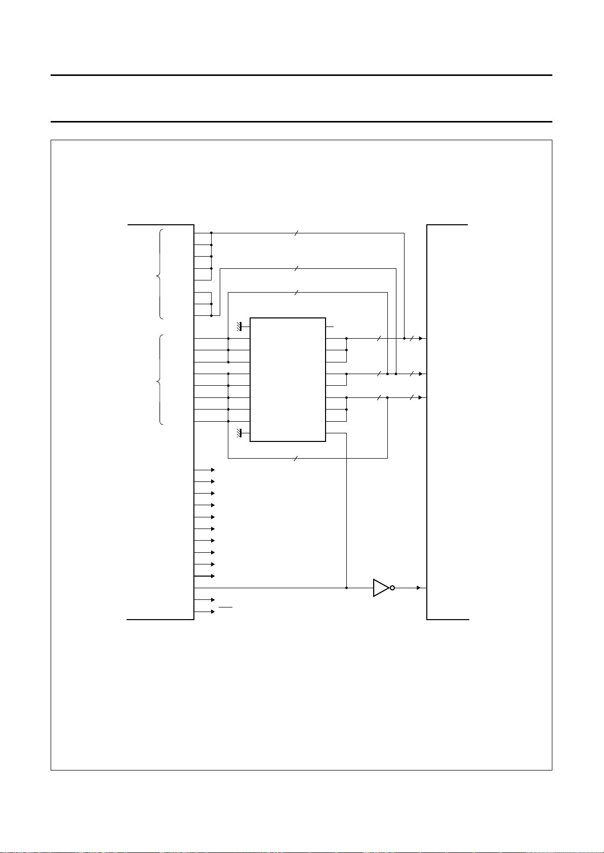
application in Fig.32).
Page 13

Philips Semiconductors Preliminary specification
Enhanced Video Input Processor (EVIP) SAA7111A
The higher output signals VPO15 to VPO8 in the YUV
format perform the digital luminance signal. The lower
output signals VPO7 to VPO0 in the YUV format are the
bits of the multiplexed colour difference signals (B−Y) and
(R−Y). The arrangement of the RGB (5, 6, 5) and
RGB (8, 8, 8) data stream bits on the VPO-bus is given in
Table 5.
The data stream format YUV4:2:2 (the 8 higher output
signals VPO15 to VPO8) in LLC data rate fulfils the
CCIR-656 standard with its own timing reference code at
the start and end of each video data block.
A pixel in the format tables is the time required to transfer
a full set of samples. If 16-bit 4 : 2 : 2 format is selected
two luminance samples are transmitted in comparison to
one (B−Y) and one (R−Y) sample within a pixel.The time
frames are controlled by the HREF signal.
Fast enable is achieved by setting input FEI to LOW.
The signal is used to control fast switching on the digital
VPO-bus. HIGH on this pin forces the VPO outputs to a
high-impedance state (see Figs 18 and 19). The I2C-bus
bit OEYC has to be set HIGH to use this function.
The digitized PAL, SECAM or NTSC signals AD1 (7 to 0)
and AD2 (7 to 0) are connected directly to the VPO-bus
via I2C-bus bit VIPB = 1 and MODE = 4, 5, 6 or 7.
AD1 (7 to 0) -> VPO (15 to 8) and
AD2 (7 to 0) -> VPO (7 to 0)
• CREF: The CREF output delivers a clock/pixel qualifier
signal for external interfaces to synchronize to the
VPO-bus data stream.
Four different modes for the clock qualifier signal are
2
selectable via the I
C-bus [subaddress 13, clock
reference output control (CCTR1 and CCTR0].
The description of CREF timing and position is
illustrated in Figs 16, 18, 20 and 21.
8.9 Synchronization
The prefiltered luminance signal is fed to the
synchronization stage. Its bandwidth is reduced to 1 MHz
in a low-pass filter. The sync pulses are sliced and fed to
the phase detectors where they are compared with the
sub-divided clock frequency. The resulting output signal is
applied to the loop filter to accumulate all phase
deviations. Internal signals (e. g. HCL and HSY) are
generated in accordance with analog front-end
requirements. The output signals HS, VS, and PLIN are
locked to the timing reference, guaranteed between the
input signal and the HREF signal, as further improvements
to the circuit may change the total processing delay. It is
therefore not recommended to use them for applications
which require absolute timing accuracy on the input
signals. The loop filter signal drives an oscillator to
generate the line frequency control signal LFCO
(see Fig.11).
The selection of the analog input channels is controlled via
I2C-bus subaddress 02 MODE select.
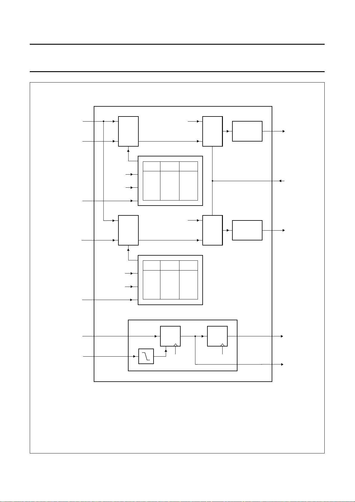
The upsampled 8-bit offset binary CVBS signal (VBI-data
bypass) is multiplexed under control of the I2C-bus to the
digital VPO-bus (see Fig.6).
8.8 Reference signals HREF, VREF and CREF
• HREF: The positive slope of the HREF output signal
indicates the beginning of a new active video line.
The high period is 720 luminance samples long and is
also present during the vertical blanking.
The description of timing and position from HREF is
illustrated in Figs 15, 16, 21 and 23.
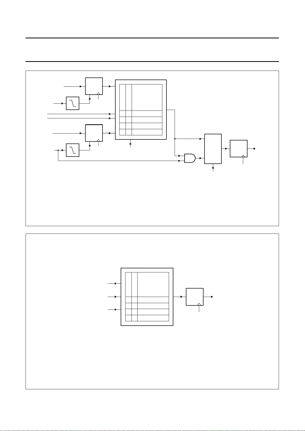
• VREF: The VREF output delivers a vertical reference
signal or an inverse composite blank signal controlled
via the I
2
C-bus [subaddress 11, inverse composite
blank (COMPO)]. Furthermore four different modes of
vertical reference signals are selectable via the I2C-bus
[subaddress 13, vertical reference output control
(VCTR1 and VCTR0)]. The description of VREF timing
and position is illustrated in Figs 15, 16, 24 and 25.
8.10 Clock generation circuit
The internal CGC generates all clock signals required for
the video input processor. The internal signal LFCO is a
digital-to-analog converted signal provided by the
horizontal PLL. It is the multiple of the line frequency
(6.75 MHz = 429/432 × f
). Internally the LFCO signal is
H
multiplied by a factor of 2 or 4 in the PLL circuit (including
phase detector, loop filtering, VCO and frequency divider)
to obtain the LLC and LLC2 output clock signals.
The rectangular output clocks have a 50% duty factor
(see Fig.26).
8.11 Power-on reset and CE input
A missing clock, insufficient digital or analog V
DDA0
supply
voltages (below 2.7 V) will initiate the reset sequence; all
outputs are forced to 3-state. The indicator output RES is
LOW for approximately 128LLC after the internal reset and
can be applied to reset other circuits of the digital TV
system.
1996 Nov 07 13
Page 14

Philips Semiconductors Preliminary specification
Enhanced Video Input Processor (EVIP) SAA7111A
It is possible to force a reset by pulling the chip enable
(CE) to ground. After the rising edge of CE and sufficient
power supply voltage, the outputs LLC, LLC2, CREF,
RTCO, RTS0, RTS1, GPSW and SDA return from 3-state
to active, while HREF, VREF, HS and VS remain in 3-state
and have to be activated via I2C-bus programming (see
Table 4).
8.12 RTCO output
The real time control and status output signal contains
serial information about the actual system clock
(increment of the HPLL), subcarrier frequency [increment
and phase (via reset) of the FSC-PLL] and PAL sequence
bit. The signal can be used for various applications in
external circuits, e.g. in a digital encoder to achieve clean
encoding (see Fig.20).
8.13 The Line-21 text slicer
The text slicer block detects and acquires Line-21 Closed
Captioning data from a 525-line CVBS signal. Extended
data services on Line-21 Field 2 are also supported.
If valid data is detected the two data bytes are stored in two
2
C-bus registers. A parity check is also performed and the
I
result is stored in the MSB of the corresponding byte.
A third I2C-bus register is provided for data valid and data
ready flags. The two bits F1VAL and F2VAL indicate that
the input signal carries valid Closed Captioning data in the
corresponding fields. The data ready bits F1RDY and
F2RDY have to be evaluated if asynchronous I2C-bus
reading is used.
8.13.1 S
UGGESTIONS FOR I
DISPLAY SOFTWARE READING LINE
2
C-BUS INTERFACE OF THE
-21 DATA
There are two methods by which the software can acquire
the data:
1. Synchronous reading once per frame (or once per
field); It can use either the rising edge (Line-21 Field 1)
or both edges (Line-21 Field 1 or 2) of the ODD signal
(pin RTSO) to initiate an I2C-bus read transfer of the
three registers 1A, 1B and 1C.
2. Asynchronous reading; It can poll either the F1RDY bit
(Line-21 Field 1) or both F1RDY/F2RDY bits (Line-21
Field 1 or 2). After valid data has been read the
corresponding F*RDY bit is set to LOW until new data
has arrived. The polling frequency has to be slightly
higher than the frame or field frequency, respectively.
1996 Nov 07 14
Page 15
Philips Semiconductors Preliminary specification
Enhanced Video Input Processor (EVIP) SAA7111A
handbook, full pagewidth
TBP7 to 0
(CVBS)
Y or YUV
BCHI1 to 0
2
I
C-bus
VBP0
VBP4
0
MUX
CVBS
1
UP
(LUMA see Fig. 37)
SWHI
BCHI1 BCHI0 SWHI
0
0
1
1
AD1BYP
0
1
0
1
1
0
VBP0
VBP4
0
1
MUX
BYP
UP
REGISTER
VPO15 to 8
VPIB
2
I
C-bus
UV or YUV
BCLO1 to 0
2
I
C-bus
V_GATE
(programmable)
HREFINT
VBP0
VBP4
0
MUX
CVBS
1
UP
(CHROMA see Fig. 37)
SWLO
BCLO1 BCLO0 SWLO
0
0
1
1
EN
AD2BYP
0
1
0
1
REG
CLOCK 0
1
0
VBP0
VBP4
0
MUX
BYP
UP
1
4 × REG
CLOCK 0
REGISTER
VPO7 to 0
VBP4
VBP0
MGG064
HREFINT = internal horizontal reference.
TBP = upsampled CVBS input data (27 MHz).
AD1BYP/AD2BYP = digitized CVBS input data and Y/C input data (13.5 MHz).
VBP0 = programmable vertical reference signal.
VBP4 = delayed programmable vertical reference signal (4LLC clocks delay).
1996 Nov 07 15
Fig.6 Multiplexing of the CVBS signal to the VPO-bus.
Page 16
Philips Semiconductors Preliminary specification
Enhanced Video Input Processor (EVIP) SAA7111A
handbook, full pagewidth
VREF CCIR 656
HREFINT
VBP0
VBP4
VREFINT
HREFINT
VREF_CCIR 656 = vertical reference signal referring to the field interval definitions of CCIR656.
HREFINT = internal horizontal reference signal.
VREFINT = internal vertical reference signal.
VBP0 = programmable vertical reference signal.
VBP4 = delayed programmable vertical reference signal (4LLC clocks delay).
REG
EN
CLOCK 0
REG
EN
CLOCK 0
V
V
C
C
T
T
R
R
0
1
0
0
VREFINT
0
1
VREF CCIR 656
1
0
VBP0
1
1
VBP4
VCTR1 to 0
VREFOUT
Fig.7 VREF output signal generation.
0
MUX
1
COMPO
REG
VREF
CLOCK 0
MGG065
handbook, full pagewidth
C
C
C
CREFINT
selected
VREF
CCTR1 to 0
CREFINT = internal clock qualifier signal.
C
T
T
R
R
0
1
0
0
0
1
1
0
1
1
CREFOUT
CREFINT
0 if VREF = 0
1 if VREF = 0
1 (always HIGH)
Fig.8 CREF output signal generation.
1996 Nov 07 16
REG
CREF
CLOCK 0
MGG066
Page 17
Philips Semiconductors Preliminary specification
Enhanced Video Input Processor (EVIP) SAA7111A
AOUT
(14) 23
AND
TEST
SELECTOR
BUFFER
ADC2
AOSL (1 : 0)
SWITCH
BYPASS
FILTER
ANTI-ALIAS
DAC9
ANALOG
AMPLIFIER
FUSE (1 : 0)
ANALOG
ADC1
SWITCH
BYPASS
FILTER
ANTI-ALIAS
DAC9
AMPLIFIER
VERTICAL
FUSE (1 : 0)
CONTROL
BLANKING
CONTROL
ANTI-ALIAS
GAIN
CONTROL
VBLNK
SVREF
VBSL 8 8
HOLDG
GAFIX
HSY
GLIMB
GLIMT
WPOFF
GAI20-GAI28
GAI10-GAI18
GUDL0-GUDL2
HLNRS
WIPA
SLTCA
AD1BYPAD2BYP
handbook, full pagewidth
CROSS MULTIPLEXER
UPTCV
Fig.9 Analog input processing.
987 (64)
n.c.
n.c.
18 (9)
n.c.
V
1996 Nov 07 17
14 (5)
SSA1
V
SSA2
CLAMP
CIRCUIT
SWITCH
SOURCE
15 (6)
17 (8)
AI22
AI21
20 (11)
16 (7)
DDA1
V
DDA2
V
CLAMP
CIRCUIT
SWITCH
SOURCE
19 (10)
21 (12)
AI12
AI11
CLAMP
CONTROL
MODE
CONTROL
HCL
MODE 0
MODE 1
MODE 2
ANALOG
CONTROL
22 (13)
SSS
V
CHRLUM
MGC655
The pin numbers given in parenthesis refer to the 64-pin package.
Page 18
Philips Semiconductors Preliminary specification
Enhanced Video Input Processor (EVIP) SAA7111A
k, full pagewidth
AD1BYPAD2BYP
sequential
SECAM
PROCESSING
UV signals
LEVEL
LOW-PASS
FEI
(52) 63
53 to 62
(42 to 51),
OUTPUT
RGB
RGB MATRIX
Y
AND
CONTRAST,
BRIGHTNESS,
ADJUSTMENT,
VPO
(9 : 0)VPO
45 to 50
(34 to 39),
AND
INTERFACE
FORMATTER
dithering
interpolation
CONTROL
SATURATION
PHASE
DETECTOR
AMPLITUDE
DEMODULATOR
HREF
(15 : 10)
(31) 42
COMB
FILTERS
DIT CBR
UV
GAIN
CONTROL
AND Y-DELAY
COMPENSATION
BURST GATE
LOOP FILTER
ACCUMULATOR
GPSW
RTSE1
OFTS0
OFTS1
SECAM
DCCF
RECOMBINATION
BRIG
CONT
CODE
FCTCCSTD 1
RTSE0
VIPB
VLOF
RGB888
OEYC
OEHV
/2 switch signal
H
f
SATN
COLO
COMPO
FECO
VRLN
RTCO
(60) 3
VSTA (8 : 0)
VSTO (8 : 0)
MGG062
Y
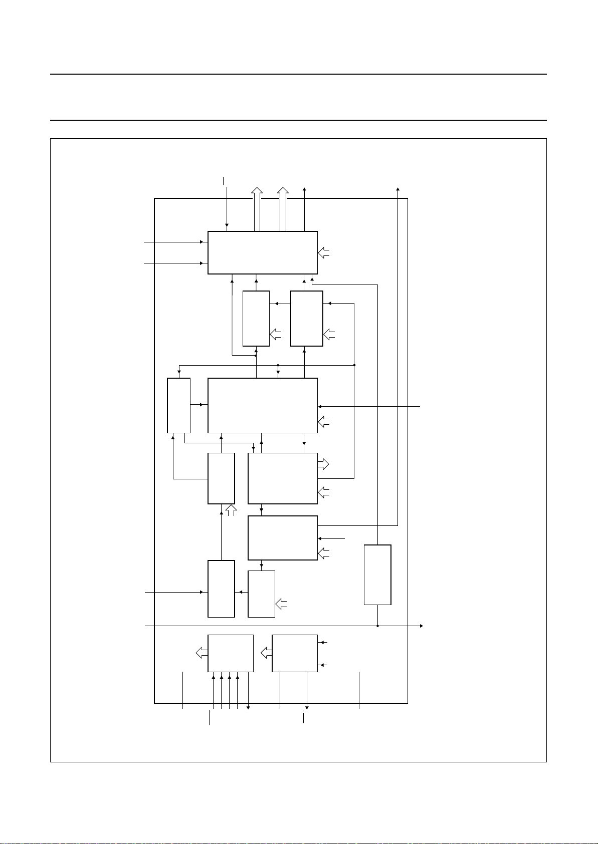
Fig.10 Chrominance circuit.
CHBW0
CHRLUM
10 (1)
DDI2C
V
CHBW1
QUADRATURE
DEMODULATOR
TEST
CONTROL
2 (59)
1 (58)
13 (4)
12 (3)
TDI
TCK
TRST
BLOCK
11 (2)
TDO
TMS
SUBCARRIER
AND
INCREMENT
SUBCARRIER
GENERATION
HUEC
GENERATION
POWER-ON
(57,41,33,
25,18)
68,52,44,
34,27
DDD1-5
V
1996 Nov 07 18
DIVIDER
CONTROL
32 (23)
RES
INCS
CSTD 0
CLOCKS
CE
(56,40,32,26,19)
TUF
VBI DATA BYPASS
67,51,43,35,28
SSD1-5
V
LUM
The pin numbers given in parenthesis refer to the 64-pin package.
Page 19
Philips Semiconductors Preliminary specification
Enhanced Video Input Processor (EVIP) SAA7111A
DDA0VSSA0
CREF
LLC
LLC2
CE
V
XTALI
XTAL
(22) 31
CLOCKS
(21)30
(20) 29
CLOCK
GENERATOR
LINE-LOCKED
(24)33
(16) 25
(15) 24
CLOCK
CIRCUIT
GENERATION
(54) 65
(55) 66
CLOCK
CRYSTAL
GENERATOR
MGC654
CLOCK CIRCUIT
DAC6
INCS
APER0
APER1
Y
AND
ADDING
STAGE
WEIGHTING
VBLB
MATCHING
AMPLIFIER
VBLB
PHASE
FINE
PHASE
DETECTOR
COARSE
DETECTOR
AUFD
HSB
HPLL
HSS
VTRC
VTRC
EXFIL
STTC
HLCK
FSEL
VTRC
TIME
DISCRETE
OSCILLATOR 2
2
LOOP FILTER
(28)
(27)
COUNTER
39
RTS1
38
HS
handbook, full pagewidth
BPSS0
BPSS1
FILTER
VARIABLE
BAND-PASS
PREF
SYNC SLICER
LUMINANCE CIRCUIT
TRAP
CHROMINANCE
LUM
PREFILTER
BYPS
VBLB
PREF
SYNC
PREFILTER
TEXT
LINE 21
1996 Nov 07 19
FIDT
VNOI0
VNOI1
VTRC
SYNCHRONIZATION CIRCUIT
BYTE1
SLICER
BYTE2
STATUS
2
I C BUS CONTROL
VERTICAL
PROCESSOR
2
I C-BUS
INTERFACE
64 (53)
GPSW
(17)
(29)
(30)
(62)
(63)
(61)
26
VREF
40
RTS0
41
VS
5
SDASCLIICSA
6
4
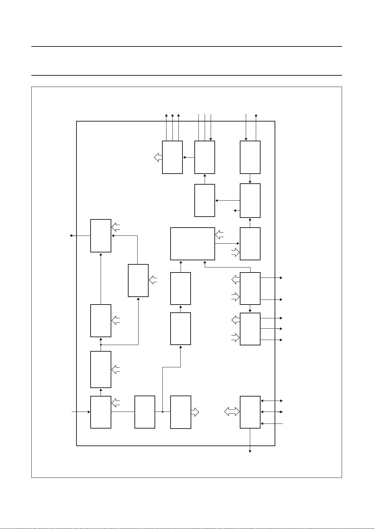
Fig.11 Luminance and sync processing.
The pin numbers given in parenthesis refer to the 68-pin package.
Page 20
Philips Semiconductors Preliminary specification
Enhanced Video Input Processor (EVIP) SAA7111A
9 GAIN CHARTS
handbook, full pagewidth
handbook, halfpage
7.5
factor
dB
5.5
3.5
bit [8] = 1
1.5
−0.5
−2.5
−4.5
0
= 20 x log10 gain =
dB
i > 256
= 20 x log10 gain =
factor
dB
(
bit [8] = 0
256 512
gain value (i)
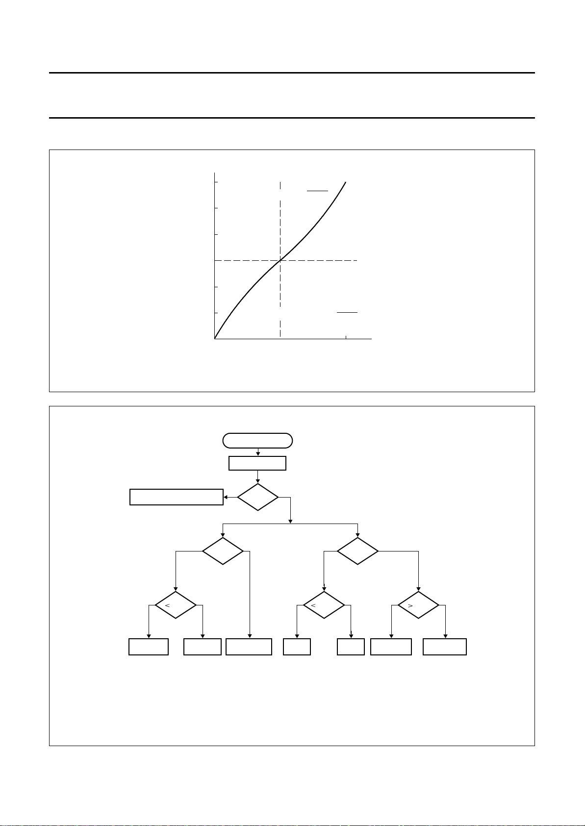
Fig.12 Amplifier curve.
ANALOG INPUT
512
768 − i
(
i < 256
(
MGC648
257 + i
512
(
ADC
NO BLANKING ACTIVE
10 10
10
CLL
+ CLAMP − CLAMP
WIPE = white peak level (254); SBOT = sync bottom level (1); CLL = clamp level [60 Y (128 C)];
HSY = horizontal sync pulse; HCL = horizontal clamp pulse.
10
VBLK
GAIN -><- CLAMP
HCL HSY
01 10
SBOT
NO CLAMP
+ GAIN − GAIN
Fig.13 Clamp and gain flow.
fast − GAIN
WIPE
slow + GAIN
MGC647
1996 Nov 07 20
Page 21
Philips Semiconductors Preliminary specification
Enhanced Video Input Processor (EVIP) SAA7111A
handbook, full pagewidth
NO ACTION
0
1
ANTI-ALIAS FILTER
0
1
<4
>248
ANALOG INPUT
AMPLIFIER
ADC
1
VBLK
1
1
>254
X = 0
0
0
HOLDG
1
<1
gain
8
0
1
X
1
0
DAC
LUMA/CHROMA DECODER
0
0
HSY
1
>254
X = 1
9
0
+1/F
STOP
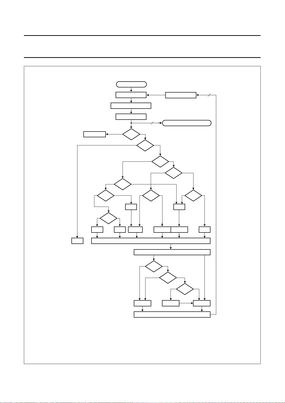
X = system variable; Y = IAGV − FGVI > GUDL; VBLK = vertical blanking pulse;
HSY = horizontal sync pulse; AGV = actual gain value; FGV = frozen gain value.
−
1/LLC2
+1/L
GAIN ACCUMULATOR (18 BITS)
ACTUAL GAIN VALUE 9-BIT (AGV) [−6/+6 dB]
1
AGV
Fig.14 Gain flow chart.
+1/LLC2 −1/LLC2
0
X
1
HSY
1
UPDATE
GAIN VALUE 9-BIT
+/− 0
0
0
Y
FGV
MGC652
1996 Nov 07 21
Page 22
Philips Semiconductors Preliminary specification
Enhanced Video Input Processor (EVIP) SAA7111A
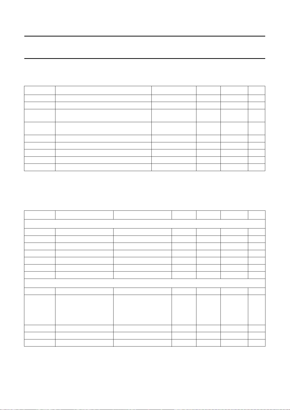
10 LIMITING VALUES
In accordance with the Absolute Maximum Rating System (IEC 134); all ground pins connected together and all supply
pins connected together.
SYMBOL PARAMETER CONDITIONS MIN. MAX. UNIT
V
DDD
V
DDA
V
i
V
o
∆V
SS
T
stg
T
amb
T
amb(bias)
V
esd
digital supply voltage −0.5 +4.6 V
analog supply voltage −0.5 +4.6 V
input voltage −0.5 VDD+ 0.5
V
(4.6 max)
output voltage −0.5 VDD+ 0.5
V
(4.6 max)
voltage difference between V
SSAall
and V
SSall
− 100 mV
storage temperature −65 +150 °C
operating ambient temperature 0 70 °C
operating ambient temperature under bias −10 +80 °C
electrostatic discharge all pins note 1 −2000 +2000 V
Note
1. Human body model: equivalent to discharging a 100 pF capacitor through a 1.5 kΩ resistor.
11 CHARACTERISTICS
= 3.0 to 3.6 V; V
V
DDD
= 3.1 to 3.5 V; T
DDA
=25°C; unless otherwise specified.
amb
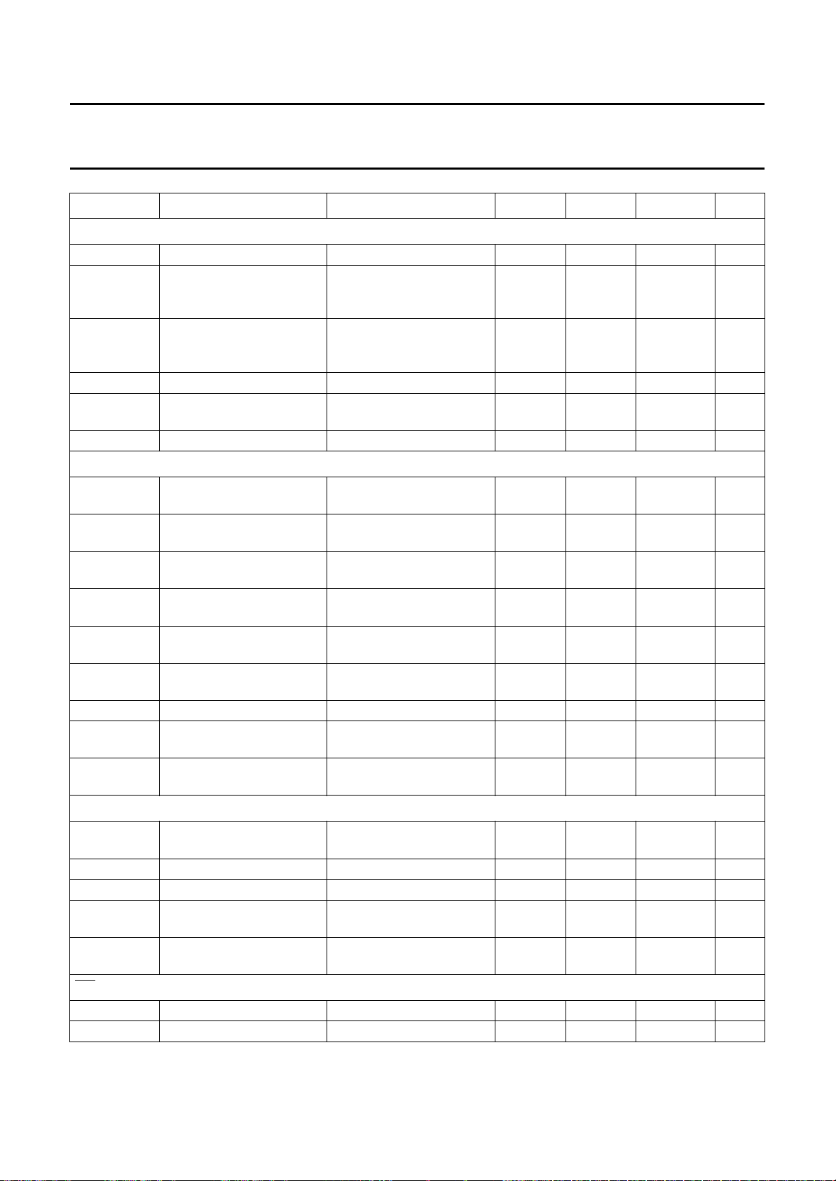
SYMBOL PARAMETER CONDITIONS MIN. TYP. MAX. UNIT
Supplies
V
I
DDD
P
V
I
DDA
P
P
DDD
D
DDA
A
A+D
digital supply voltage 3.0 3.3 3.6 V
digital supply current − 70 75 mA
digital power − 0.26 − W
analog supply voltage 3.1 3.3 3.5 V
analog supply current − 69 − mA
analog power − 0.24 − W
analog and digital power − 0.5 − W
Analog part
I
clamp
V
i(p-p)
clamping current VI= 0.9 V DC −±3.5 −µA
input voltage
(peak-to-peak value)
for normal video levels
[1 V (p-p)]; −3dB
0.3 0.7 1.2 V
termination 27/47 Ω and
AC coupling required;
coupling capacitor = 22 nF
| input impedance clamping current off 200 −− kΩ
|Z
i
C
i
α
cs
input capacitance −−10 pF
channel crosstalk fi= 5 MHz −−−50 dB
1996 Nov 07 22
Page 23
Philips Semiconductors Preliminary specification
Enhanced Video Input Processor (EVIP) SAA7111A
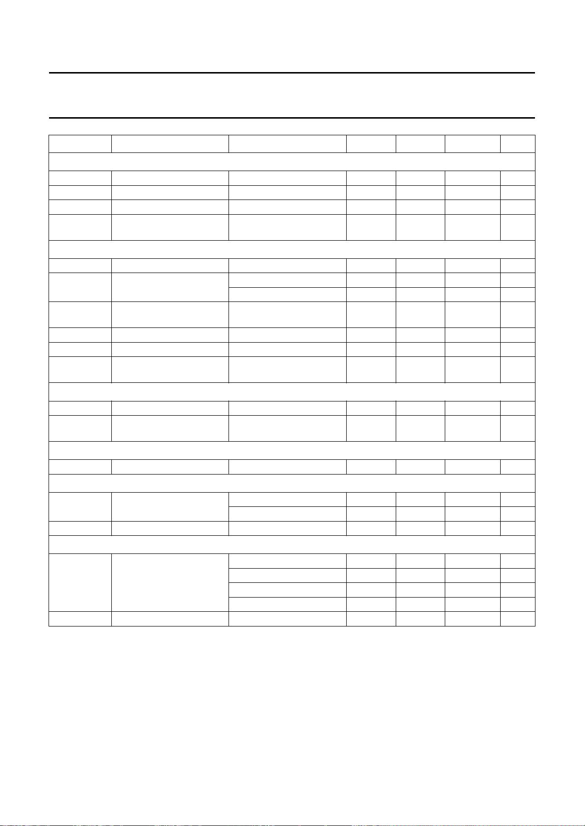
SYMBOL PARAMETER CONDITIONS MIN. TYP. MAX. UNIT
Analog-to-digital converters
B bandwidth at −3dB − 15 − MHz
φ
diff
differential phase
(amplifier plus anti-alias
filter = bypass)
G
diff
differential gain
(amplifier plus anti-alias
filter = bypass)
f
clkADC
ADC clock frequency 12.8 − 14.3 MHz
DLE DC differential linearity
error
ILE DC integral linearity error − 1 − LSB
Digital inputs
V
IL(SCL,SDA)
LOW level input voltage
pins SDA and SCL
V
IH
HIGH level input voltage
pins SDA and SCL
V
IL(xtal)
LOW level CMOS input
voltage pin XTALI
V
IH(xtal)
HIGH level CMOS input
voltage pin XTALI
V
ILn
LOW level input voltage all
other inputs
V
IHn
HIGH level input voltage
all other inputs
I
LI
C
i
input leakage current −−1 µA
input capacitance inputs and outputs at
high-impedance
C
i(n)
input capacitance all other
inputs
− 2 − deg
− 2 − %
− 0.7 − LSB
−0.5 − +0.3V
0.7V
DDD
− V
DDD
DDD
+ 0.5 V
V
−−− V
−−− V
−0.3 − +0.8 V
2.0 − V
DDD
+ 0.3 V
−−8pF
−−5pF
Digital outputs
V
OL(SCL,SDA)
LOW level output voltage
pins SDA and SCL
V
OL
V
OH
V
OL(clk)
LOW level output voltage V
HIGH level output voltage V
LOW level output voltage
for clocks
V
OH(clk)
HIGH level output voltage
for clocks
FEI input timing
t
SU;DAT
t
HD;DAT
input data set-up time 13 −− ns
input data hold time 3 −− ns
1996 Nov 07 23
SDA/SCL at 3 mA (6 mA)
−−0.4 (0.6) V
sink current
= min, IOL= −2mA 0 − 0.4 V
DDD
= min, IOL= −2 mA 0.85V
DDD
−− V
DDD
−0.5 − +0.6 V
2.4 − V
DDD
+ 0.5 V
Page 24
Philips Semiconductors Preliminary specification
Enhanced Video Input Processor (EVIP) SAA7111A
SYMBOL PARAMETER CONDITIONS MIN. TYP. MAX. UNIT
Data and control output timing; note 1
C
L
t
OHD;DAT
t
PD
t
PDZ
Clock output timing (LLC and LLC2); note 2
C
L(LLC)
T
cy
δ
LLC
t
r
t
f
t
d
output load capacitance 15 − 40 pF
output hold time CL=15pF 4 −− ns
propagation delay CL=25pF −−20 ns
propagation delay to
−−20 ns
3-state
output load capacitance 15 − 40 pF
cycle time LLC 35 − 39 ns
LLC2 70 − 78 ns
duty factors for t
and t
LLC2H/tLLC2
LLCH/tLLC
CL=25pF 40 − 60 %
rise time LLC, LLC2 −−5ns
fall time LLC, LLC2 −−5ns
delay time LLC output to
LLC2 output
at 1.5 V;
LLC/LLC2 = 25 pF
−4 − +8 ns
Data qualifier output timing (CREF)
t
OHD;CREF
t
PD;CREF
output hold time CL=15pF 4 −− ns
propagation delay from
positive edge of LLC
Clock input timing (XTALI)
δ
XTALI
duty factor for t
XTALIH/tXTALI
Horizontal PLL
f
Hn
∆fH/f
Hn
nominal line frequency 50 Hz field − 15625 − Hz
permissible static deviation −−5.7 %
Subcarrier PLL
f
SCn
nominal subcarrier
frequency
∆f
SC
lock-in range ±400 −− Hz
CL=25pF −−20 ns
nominal frequency 40 − 60 %
60 Hz field − 15734 − Hz
PAL BGHI − 4433619 − Hz
NTSC M; NTSC-Japan − 3579545 − Hz
PAL M − 3575612 − Hz
PAL N − 3582056 − Hz
1996 Nov 07 24
Page 25
Philips Semiconductors Preliminary specification
Enhanced Video Input Processor (EVIP) SAA7111A
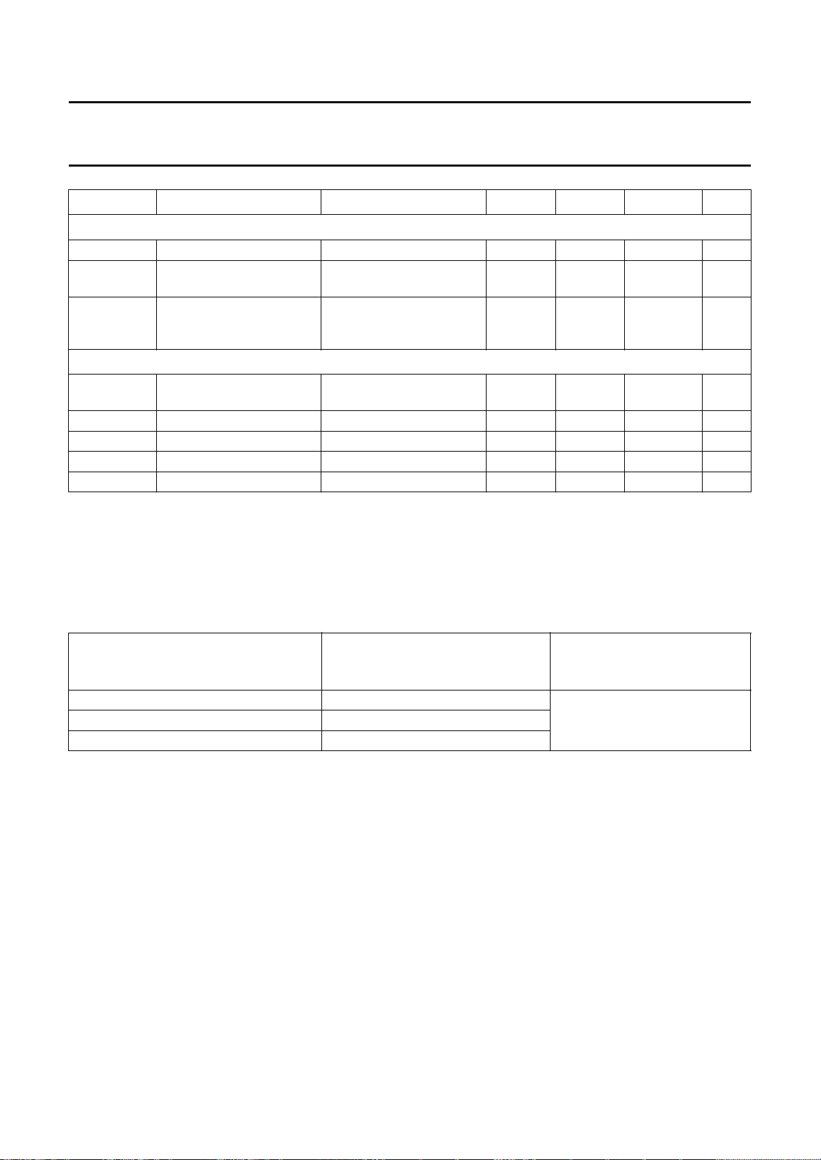
SYMBOL PARAMETER CONDITIONS MIN. TYP. MAX. UNIT
Crystal oscillator
f
n
∆f/f
n
∆Tf/f
n
CRYSTAL SPECIFICATION (X1)
T
amb(X1)
C
L
R
s
C
1
C
0
Notes
1. The levels must be measured with load circuits; 1.2 kΩ at 3 V (TTL load); CL= 50 pF.
2. The effects of rise and fall times are included in the calculation of t
drawings and conditions illustrated in Figs 15 and 16.
3. Order number: Philips 4322 143 05291.
nominal frequency 3rd harmonic; note 3 − 24.576 − MHz
permissible nominal
−−±50 10
−6
frequency deviation
permissible nominal
−−±20 10
−6
frequency deviation with
temperature
operating ambient
0 − 70 °C
temperature
load capacitance 8 −− pF
series resonance resistor − 40 80 Ω
motional capacitance − 1.5 ±20% − fF
parallel capacitance − 3.5 ±20% − pF
OHD;DAT
, tPD and t
. Timings and levels refer to
PDZ
Table 1 Processing delay
FUNCTION
TYPICAL ANALOG DELAY
AI22 −> ADCIN (AOUT) (ns)
Without amplifier or anti-alias filter 15
With amplifier and anti-alias filter 75
DIGITAL DELAY
ADCIN −> VPO (LLC CLOCKS)
[YDEL(2 to 0) = 000]
179With amplifier, without anti-alias filter 25
1996 Nov 07 25
Page 26
Philips Semiconductors Preliminary specification
Enhanced Video Input Processor (EVIP) SAA7111A
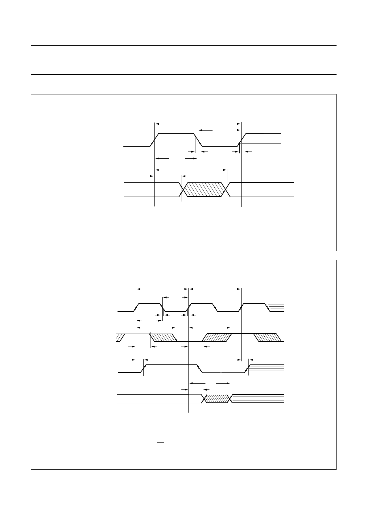
12 TIMING DIAGRAMS
t
handbook, full pagewidth
CLOCK OUTPUT LLC
OUTPUTS VPO, HREF,
VREF, VS, HS
t
t
OHD;DAT
LLCH
LLC
t
LLCL
t
f
t
PD
t
r
2.6 V
1.5 V
0.6 V
MGC658
2.4 V
0.6 V
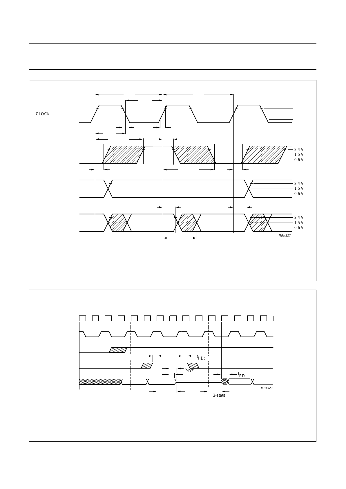
An explanation of the output formats is given in Table 5.
Fig.15 Clock/data timing (8-bit CCIR-656 format of the VPO-bus).
handbook, full pagewidth
CLOCK OUTPUT LLC
OUTPUT CREF
CLOCK OUTPUT LLC2
OUTPUTS VPO, HREF,
VREF, VS, HS
t
LLCH
t
OHD;CREF
t
dLLC2
t
LLC
t
PD
t
OHD;DAT
t
LLCL
t
f
t
r
t
OHD;CREF
t
t
PD
PD
t
LLC
t
dLLC2
MGC659
2.6 V
1.5 V
0.6 V
2.4 V
0.6 V
2.6 V
1.5 V
0.6 V
2.4 V
0.6 V
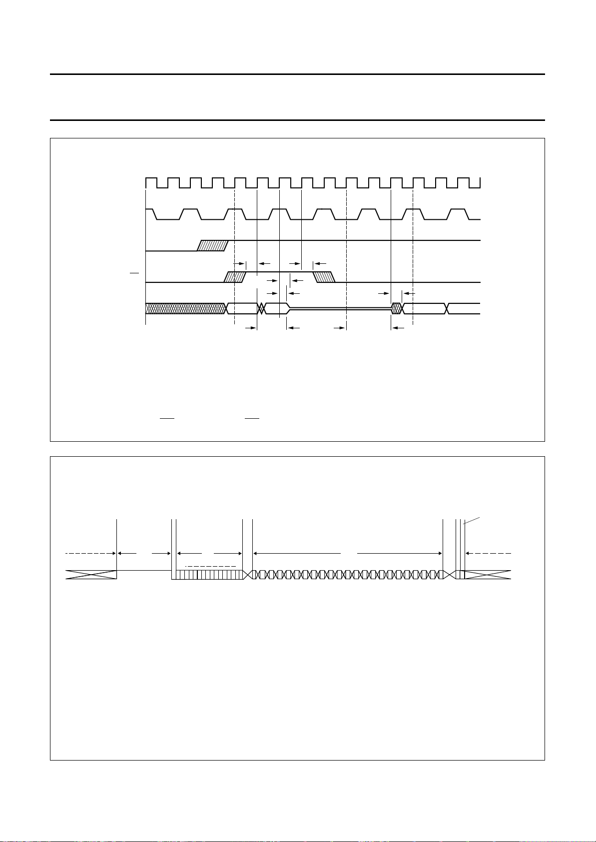
An explanation of the output formats is given in Table 5. The FEI timing of the VPO-bus is illustrated in Figs 18 and 19.
1996 Nov 07 26
Fig.16 Clock/data timing (12 and 16-bit CCIR-601 format of the VPO-bus).
Page 27
Philips Semiconductors Preliminary specification
Enhanced Video Input Processor (EVIP) SAA7111A
handbook, full pagewidth
CLOCK OUTPUT LLC
t
LLCH
t
PD;CREF
OUTPUT CREF
t
OHD;CREF
RGB (8, 8, 8) data
VPO15 to VPO8
RGB (8, 8, 8) data
VPO7 to VPO0
An explanation of the output formats is given in Table 5.
t
LLC
t
LLCL
t
f
R(2 : 0)
G(1 : 0)
B(2 : 0)
t
r
R(7 : 3)
G(7 : 5)
t
t
OHD;CREF
t
PD;CREF
t
OHD;DAT
PD
t
LLC
G(4 : 2)
B(7 : 3)
t
OHD;CREF
t
OHD;DAT
MBH227
2.4 V
1.5 V
0.6 V
2.4 V
1.5 V
0.6 V
2.4 V
1.5 V
0.6 V
2.4 V
1.5 V
0.6 V
handbook, full pagewidth
I2C-bus bit FECO = 1.
Fig.17 Clock/data timing for RGB (8, 8, 8) output format.
LLC
CREF
HREF
FEI
VPO
t
SU;DAT
t
OHD;DAT
to 3-state
t
PDZ
t
HD;DAT
from 3-state
t
PD
Fig.18 FEI timing diagram (FEI sampling at CREF = HIGH) for OFTS = 0, 1 or 2).
MGC656
1996 Nov 07 27
Page 28
Philips Semiconductors Preliminary specification
Enhanced Video Input Processor (EVIP) SAA7111A
handbook, full pagewidth
LLC
CREF
HREF
t
SU;DAT
FEI
VPO
Timing is compatible with SAA7110; I2C-bus bit FECO = 0.
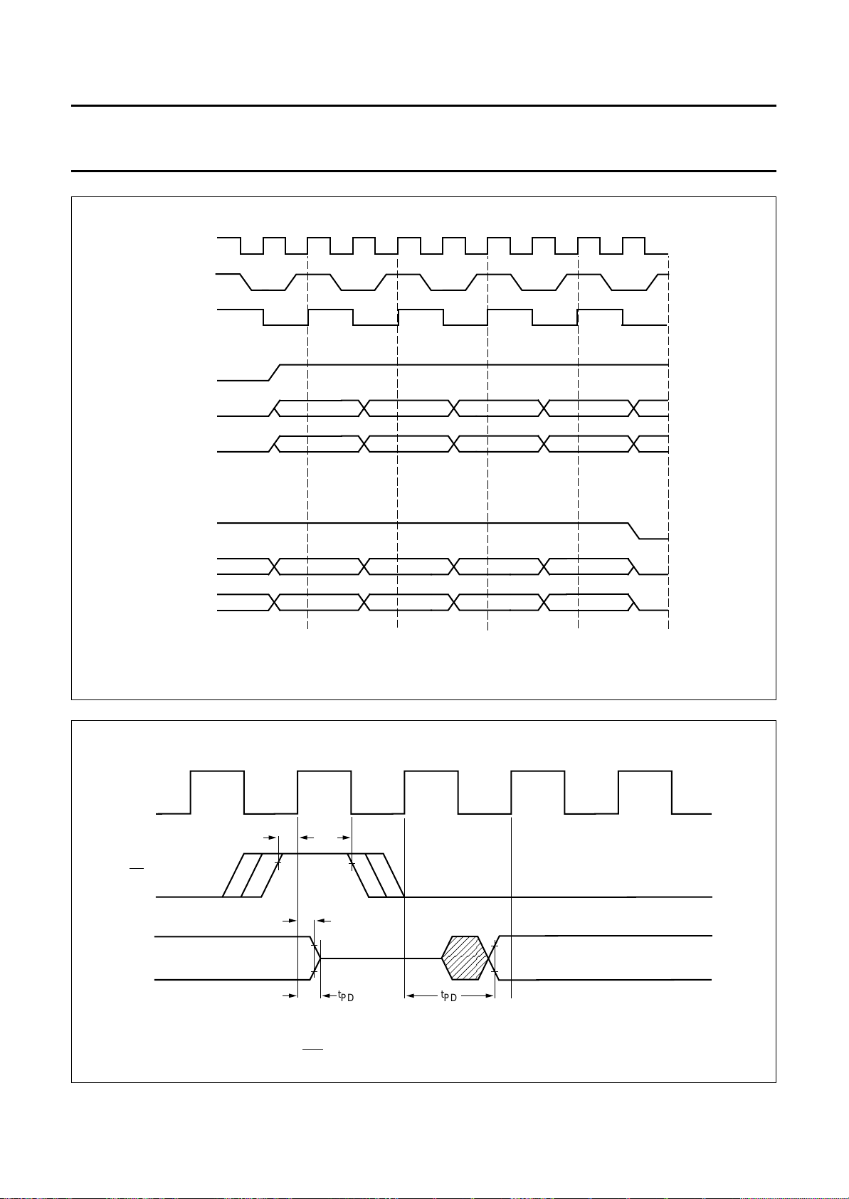
Fig.19 FEI timing diagram (FEI sampling at CREF = LOW) for OFTS = 0, 1 or 2).
t
PDZ
to 3-state
t
OHD;DAT
t
HD;DAT
from 3-state
t
PD
MGC657
handbook, full pagewidth
transmitted once per line
SEQUENCE
LOW
HIGH
128
BIT NO.:
TIME SLOT:
INCR
HPLL
INCR
FSCPLL
RESERVED
16
15
1
0 67
2
0
21
22
19
16
1617
1920
15
18
45
9
13
14
11 1012
6
8
7
3
452
3
0
1
63
50 Hz fields: 235
RESERVED
60 Hz fields: 232
1
68
(1) Set to zero for one transmission, if a phase reset of the fsc- DTO is applied via I2C-bus bit CDTO. RTCO sequence is generated in LLC/4.
The HPLL increment represents the actual LFCO frequency (f
INCR
=
f
-------------------------------------------------
LFCO
Where: f
The f
2
XTAL
increment represents the actual subcarrier frequency (related to the actual clock); 23 LSB from 24, MSB is 0b.
sc
INCR
f
-------------------------------------------------------
sc
×
HPLLfXTAL
word length DTO2
= 24.576 MHz, word length DTO2 = 20 bits.
FSCPLLfXTAL
word length DTO1
2
×
INCR
×=
---------------------------2
HPLL
19
LFCO
× 4=f
); 16 LSB from 20, upper four bits are fixed to 0100b
LLC
Where: word length DTO1 = 24 bits.
Fig.20 Real time control output.
1996 Nov 07 28
DTO RESET
RESERVED
MGC649
(1)
Page 29
Philips Semiconductors Preliminary specification
Enhanced Video Input Processor (EVIP) SAA7111A
handbook, full pagewidth
LLC
CREF
LLC2
HREF
Yn
UVn
HREF
Yn
UVn
START OF ACTIVE LINE
0
U0 V0 U2 V2 U4
1234
END OF ACTIVE LINE
719718717716715
V716U716V714
U718 V718
MGC646
handbook, full pagewidth
LLC
FEI
VPO
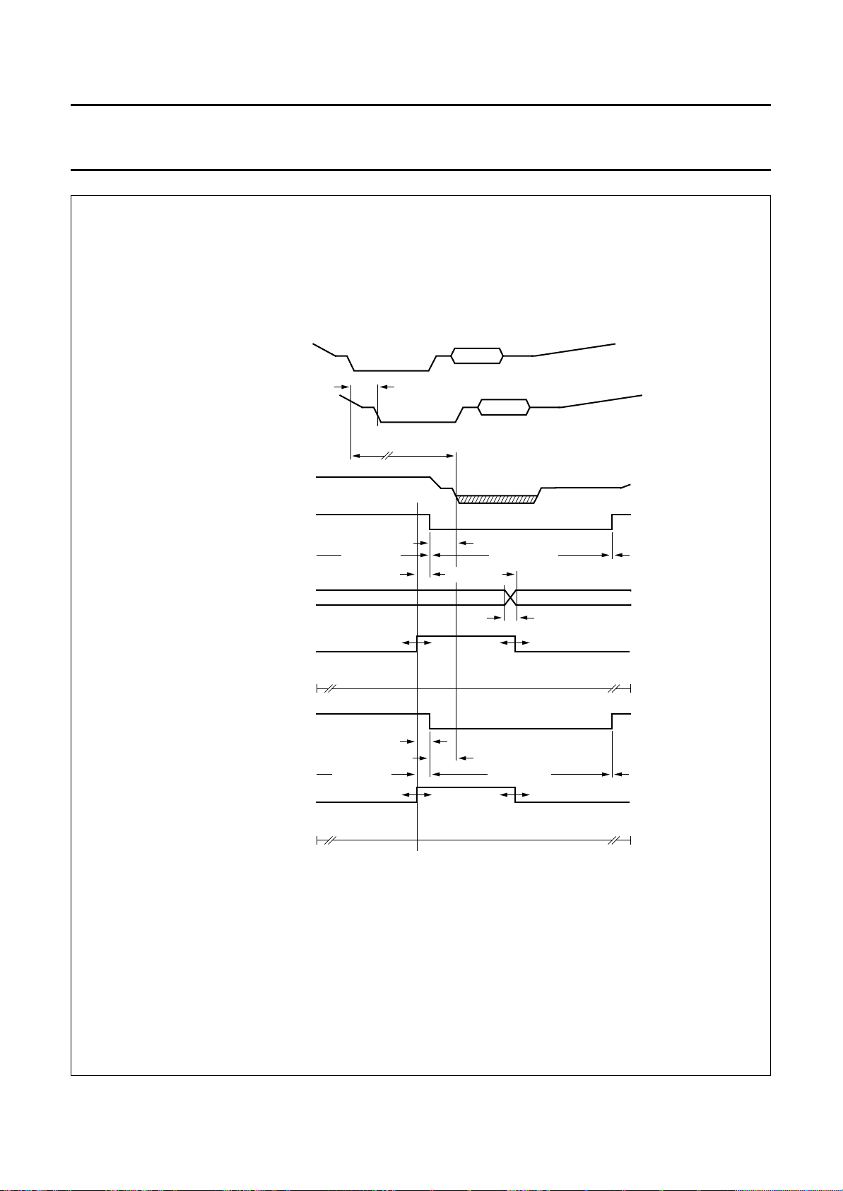
Fig.21 HREF timing diagram.
t
SU
t
HD
t
OHD
t
PDZ
t
PD
Fig.22 FEI timing in CCIR 656 mode [OFTS (1 : 0) = 3].
MBH766
1996 Nov 07 29
Page 30
Philips Semiconductors Preliminary specification
Enhanced Video Input Processor (EVIP) SAA7111A
handbook, full pagewidth
CVBS
VBI
Y - output
HREF (50 Hz)
RTS1 (PLIN)
HS
HS (50 Hz)
programming range
(step size: 8/LLC)
HREF (60 Hz)
HS (60 Hz)
(1)
108
720 × 2/LLC
179 × 1/LLC
720 × 2/LLC
27 × 2/LLC
23 × 2/LLC
26 × 1/LLC
0
0
burst
burst
processing delay CVBS->VPO
sync clipped
12 × 2/LLC
144 × 2/LLC
43 × 2/LLC
4/LLC
16 × 2/LLC
138 × 2/LLC
(2)
−107
(1) PLIN is switched to output RTS1 via I2C-bus bit RTSE1 = 0.
(2) See Table 1.
(3) HDEL (1 : 0) = 0 0, YDEL (2 : 0) = 0 0 0.
1996 Nov 07 30
HS (60 Hz)
programming range
(step size: 8/LLC)
107
0
Fig.23 Horizontal timing diagram.
−106
MGD701
Page 31
Philips Semiconductors Preliminary specification
Enhanced Video Input Processor (EVIP) SAA7111A
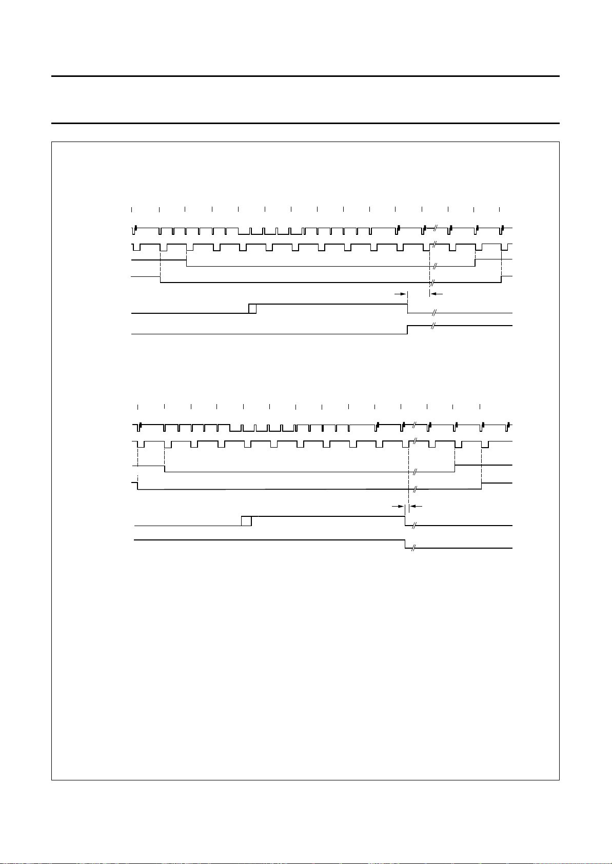
handbook, full pagewidth
input CVBS
HREF
VREF
VREF
VS
RTS0 (ODD)
input CVBS
HREF
VREF
VREF
VS
622
VRLN = 1
VRLN = 0
(1)
VRLN = 1
VRLN = 0
310
623
624
(2)
(2)
312
311
(2)
(2)
1234567822625
313 314
(a) 1st field
315 316
317
318
319
320
535 x 2/LLC
335 336
77 x 2/LLC
23
337
RTS0 (ODD)
(1) ODD is switched to output RTS0 via I2C-bus bit RTSE0 = 0.
(2) Additional VREF positions can be achieved via I2C-bits VCTR1 and VCTR0 (see Fig.7).
The luminance peaking and the chrominance trap are bypassed during VREF = 0 if I2C-bus bit VBLB is set to logic 1.
The chrominance delay line (chrominance-comb filter for NTSC, phase error correcting for PAL) is disabled during VREF = 0.
(1)
(b) 2nd field
Fig.24 Vertical timing diagram for 50 Hz [nominal input signal VNL in normal mode (VNOI = 00b)].
1996 Nov 07 31
MGG069
Page 32
Philips Semiconductors Preliminary specification
Enhanced Video Input Processor (EVIP) SAA7111A
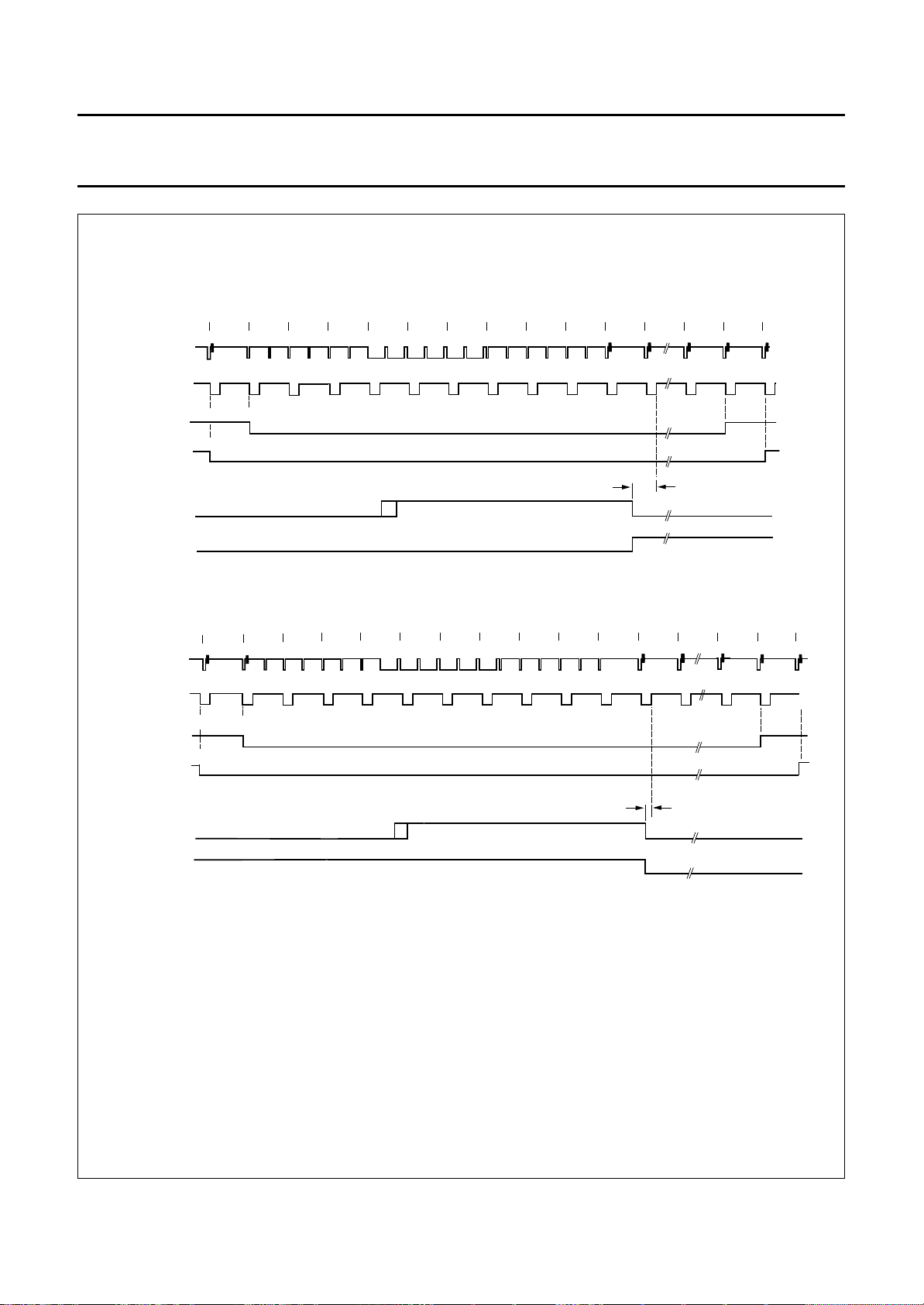
1234567
handbook, full pagewidth
input CVBS
HREF
VREF
VREF
VS
522
(525)
VRLN = 1
VRLN = 0
523
(3)
(3)
(3)
(2)(1)
(4) (5) (6) (7) (8) (9)
(10)
525
524
8
(11)
520 x 2/LLC
17
(20)
18 19
(21)
(22)
(2)
RTS0 (ODD)
input CVBS
HREF
VREF
VREF
RTS0 (ODD)
(1)
VS
(1)
259
(262)
VRLN = 1
VRLN = 0
(263)
(3)
(3)
260
261
(264)
(a) 1st field
263 264 265 266 267 268 269 270 271
262
(266) (267) (268) (269) (270) (271) (272) (273) (274)
(265)
(b) 2nd field
81 x 2/LLC
280
(283)
281
(284)
MGG070
282
(285)
(2)
(1) ODD is switched to output RTS0 via I2C-bus bit RTSE0 = 0.
(2) Line numbers in parenthesis refer to CCIR line counting.
(3) Additional VREF positions can be achieved via I2C-bus bits VCTR1 and VCTR0 (see Fig.7).
The luminance peaking and the chrominance trap are bypassed during VREF = 0 if I2C-bus bit VBLB is set to logic 1.
The chrominance delay line (chrominance-comb filter for NTSC, phase error correcting for PAL) is disabled during VREF = 0.
Fig.25 Vertical timing diagram for 60 Hz [nominal input signal VNL in normal mode (VNOI = 00b)].
1996 Nov 07 32
Page 33
Philips Semiconductors Preliminary specification
Enhanced Video Input Processor (EVIP) SAA7111A
Table 2 Digital output control
VPO
OEYC FEI
15 to 0
00 Z
1 0 active
01 Z
11 Z
13 CLOCK SYSTEM
13.1 Clock generation circuit
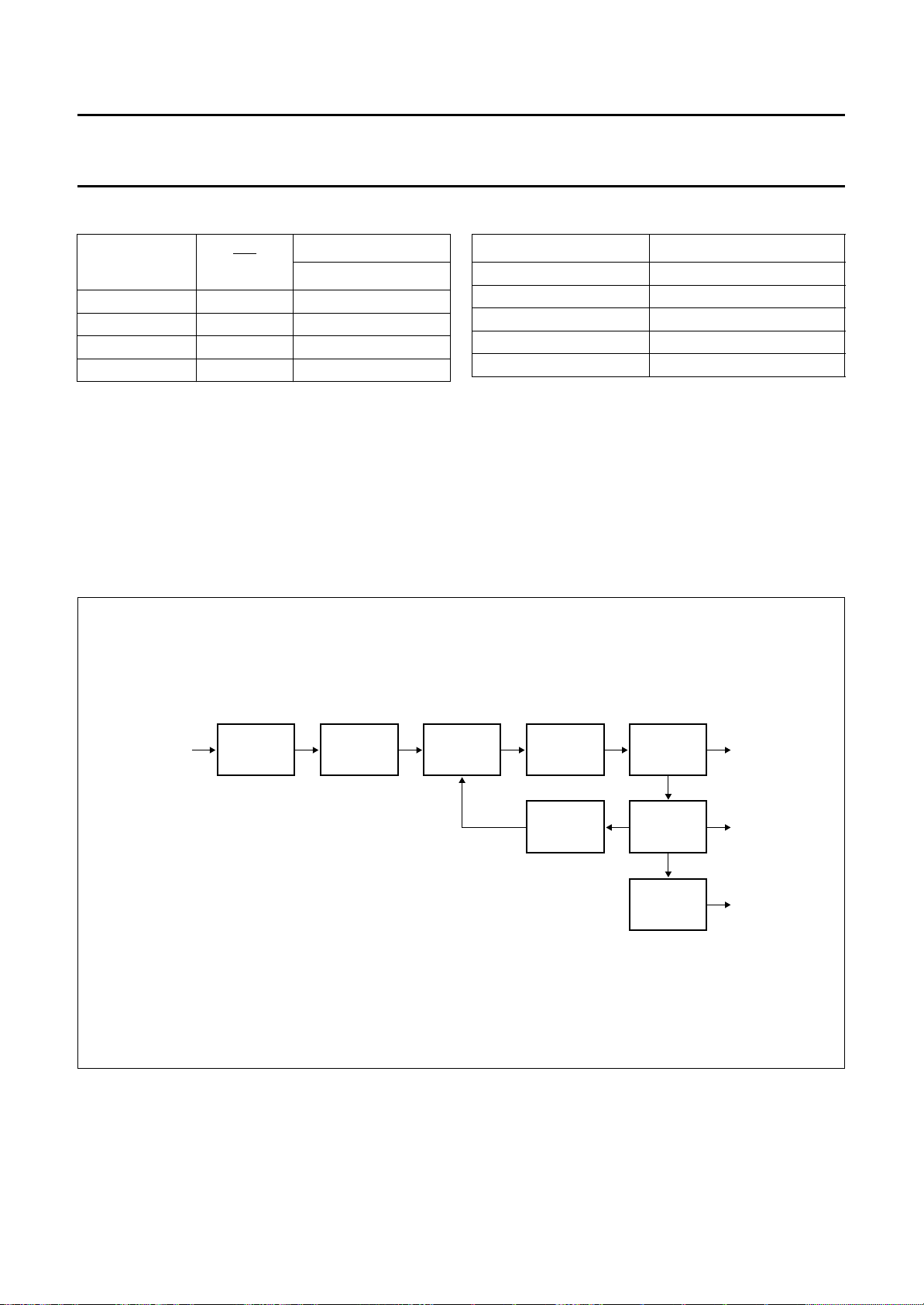
The internal CGC generates the system clocks LLC, LLC2
and the clock reference signal CREF. The internally
generated LFCO (triangular waveform) is multiplied by
2 or 4 via the analog PLL (including phase detector, loop
filter, VCO and frequency divider). The rectangular output
signals have a 50% duty factor.
Table 3 Clock frequencies
CLOCK FREQUENCY (MHz)
XTAL 24.576
LLC 27
LLC2 13.5
LLC4 6.75
LLC8 3.375
handbook, full pagewidth
LFCO
BAND PASS
FC = LLC/4
ZERO
CROSS
DETECTION
PHASE
DETECTION
LOOP
FILTER
DIVIDER
1/2
Fig.26 Block diagram of clock generation circuit.
OSCILLATOR
DIVIDER
1/2
DELAY CREF
MGC632
LLC
LLC2
1996 Nov 07 33
Page 34
Philips Semiconductors Preliminary specification
Enhanced Video Input Processor (EVIP) SAA7111A
13.2 Power-on control
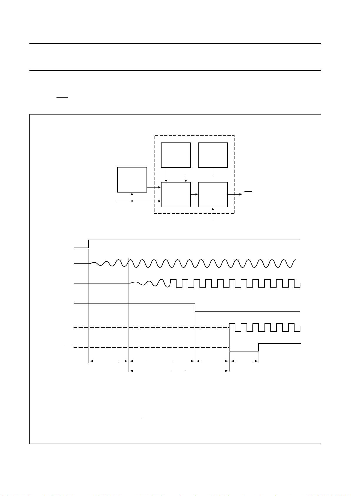
Power-on reset is activated at power-on, chip enable, PLL clock generation failure and if the supply voltage falls below
2.7 V. The RES signal can be applied to reset other circuits of the digital picture processing system.
handbook, full pagewidth
CE
XTAL
LLCINT
RESINT
CE
CLOCK
PLL
LLC
POC V
ANALOG
POC
LOGIC
DDA
POC V
DIGITAL
POC
DELAY
CLK0
DDD
RES
LLC
RES
CE = chip enable input; XTAL = crystal oscillator output; LLCINT = internal system clock;
RESINT = internal reset; LLC = line-locked clock output;
1996 Nov 07 34
some ms
20 to 200 µs
PLL-delay
<
1 ms
RES = reset output (active LOW).
896 LCC
digital delay
Fig.27 Power-on control circuit.
128 LCC
MGC633
Page 35
Philips Semiconductors Preliminary specification
Enhanced Video Input Processor (EVIP) SAA7111A
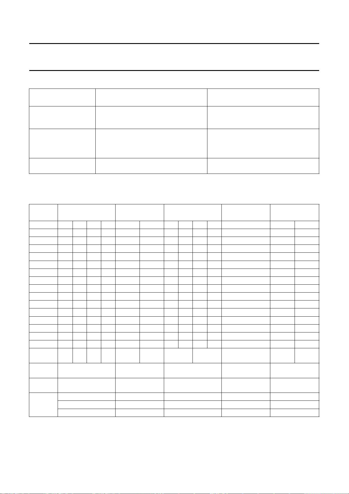
Table 4 Power-on control sequence
INTERNAL POWER-ON
CONTROL SEQUENCE
Directly after power-on
asynchronous reset
VPO15 to VPO0, RTCO, RTS0, RTS1,
GPSW, HREF, VREF, HS, VS, LLC, LLC2
and CREF are in high-impedance state
Synchronous reset
sequence
LLC, LLC2, CREF, RTCO, RTS0, RTS1,
GPSW and SDA become active;
VPO15 to VPO0, HREF, VREF, HS and VS
are held in high-impedance state
Status after power-on
control sequence
VPO15 to VPO0, HREF, VREF, HS and VS
are held in high-impedance state
14 OUTPUT FORMATS
Table 5 Output formats
BUS
SIGNAL
VPO15 Y07Y17Y27Y
VPO14 Y
VPO13 Y
VPO12 Y
VPO11 Y
VPO10 Y
VPO9 Y
VPO8 Y
VPO7 U
VPO6 U
VPO5 V
VPO4 V
411 (12-BIT) 422 (16-BIT)
37
06Y16Y26Y36
05Y15Y25Y35
04Y14Y24Y34
03Y13Y23Y33
02Y12Y22Y32
01Y11Y21Y31
00Y10Y20Y30
07U05U03U01
06U04U02U00
07V05V03V01
06V04V02V00
VPO3 X X X X U
VPO2 X X X X U
VPO1 X X X X U
VPO0 X X X X U
Pixel
0123 0 1 0 1 − note 5 note 4
order Y
Pixel
000−−
order UV
Data
LLC2 LLC2 LLC LLC2 −
rates
I2C-bus
control
signals
OFTS0 = 0 OFTS0 = 1 OFTS0 = 1 OFTS0 = 0 OFTS0 = 0
OFTS1 = 1 OFTS1 = 0 OFTS1 = 1 OFTS1 = 0 OFTS1 = 0
RGB888 = X RGB888 = X RGB888 = X RGB888 = 0 RGB888 = 1
PIN OUTPUT STATUS FUNCTION
direct switching to high impedance for
20 to 200 ms
internal reset sequence
after power-on (reset sequence) a complete
2
C-bus transmission is required
I
(1)
CCIR-656 (8-BIT)
Y
07
Y
06
Y
05
Y
04
Y
03
Y
02
Y
01
Y
00
U
07
U
06
U
05
U
04
03
02
01
00
Y
Y
Y
Y
Y
Y
Y
Y
V
V
V
V
V
V
V
V
U07Y07V07Y
17
U06Y06V06Y
16
U05Y05V05Y
15
U04Y04V04Y
14
U03Y03V03Y
13
U02Y02V02Y
12
U01Y01V01Y
11
U00Y00V00Y
10
07
06
05
04
03
02
01
00
XXXX G2 G4 R2
XXXX G1 G3 R1
XXXX G0 G2 R0
XXXX B4 B7 G1
XXXX B3 B6 G0
XXXX B2 B5 B2
XXXX B1 B4 B1
XXXX B0 B3 B0
(2)
RGB (16-BIT)
17
16
15
14
13
12
11
10
(3)
R4 R7 R7
R3 R6 R6
R2 R5 R5
R1 R4 R4
R0 R3 R3
G5 G7 G7
G4 G6 G6
G3 G5 G5
RGB (24-BIT)
(3)
1996 Nov 07 35
Page 36
Philips Semiconductors Preliminary specification
Enhanced Video Input Processor (EVIP) SAA7111A
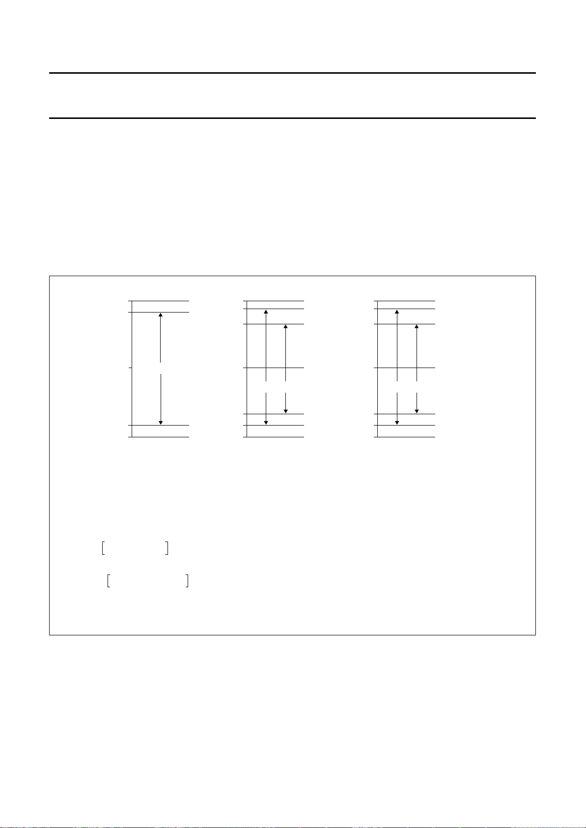
Notes to Table 5
1. Values in accordance with CCIR 601.
2. Before and after the video data, video timing codes are inserted in accordance with CCIR 656.
a) VPO15 to VPO8 = VPO7 to VPO0 = CCIR 656 data if I2C-bus bit TCLO = 0
b) VPO15 to VPO8 = CCIR 656 data, VPO7 to VPO0 = 3-state if I2C-bus bit TCLO = 1.
3. During HREF = LOW RGB levels are set to 16 (10 hex). RGB 16-bit is achieved by dropping the LSBs of the 8-bit
signals (after dithering if desired).
4. CREF = 1 (see Fig.17).
5. CREF = 0 (see Fig.17).
handbook, full pagewidth
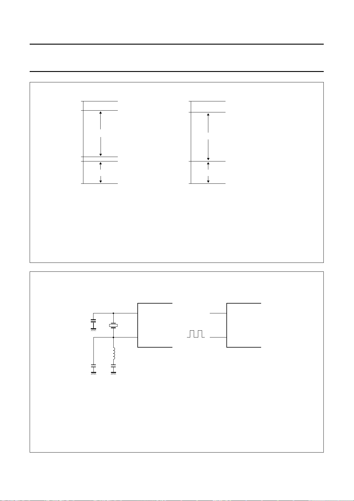
CCIR Rec. 602 digital levels.
Equations for modification to the YUV levels via BCS control I2C-bus bytes BRIG, CONT and SATN.
Luminance:
Y
OUT
Chrominance:
UV
OUT
It should be noted that the resulting levels are limited to 1 to 254 in accordance with CCIR-601/656 standard.
+255
+235
LUMINANCE 100%
+128
+16
0
(a) Y output range. (b) U output range (Cb). (c) V output range (Cr).
CONT
Int
----------------- -
Int
71
SATN
---------------- 64
Y128–()× BRIG+=
Cr Cb, 128–()× 128+=
white
black
+255
+240
+212 +212
+128
U-COMPONENT
+44
+16
0
blue 100%
blue 75%
colourless
yellow 75%
yellow 100%
+255
+240
+128
+44
+16
V-COMPONENT
0
red 100%
red 75%
colourless
cyan 75%
cyan 100%
MGC634
1996 Nov 07 36
Fig.28 VPO output signal range with default BCS settings.
Page 37
Philips Semiconductors Preliminary specification
Enhanced Video Input Processor (EVIP) SAA7111A
handbook, full pagewidth
VBI data levels are not dependent on BCS settings.
+255
+209
LUMINANCE
+71
+60
SYNC
1
(a) For sources containing 7.5 IRE black level offset
(e.g. NTSC−M).
+255
white
black
black shoulder
sync bottom
+199
LUMINANCE
+60
1
(b) For sources not containing black level offset.
Fig.29 VBI data bypass output range.
white
black shoulder = black
SYNC
sync bottom
MGD700
handbook, full pagewidth
The pin numbers given in parenthesis refer to the 64-pin package.
Order number: Philips 4322 143 05291.
quartz (3rd harmonic)
24.576 MHz
C =
10 pF
C =
10 pF
(a) With quartz crystal. (b) With external clock.
XTAL
65 (54)
XTALI
66 (55)
L = 10 µH ±20%
C =
1 nF
SAA7111A SAA7111A
Fig.30 Oscillator application.
1996 Nov 07 37
XTAL
XTALI
65 (54)
66 (55)
MGG072
Page 38
Philips Semiconductors Preliminary specification
Enhanced Video Input Processor (EVIP) SAA7111A
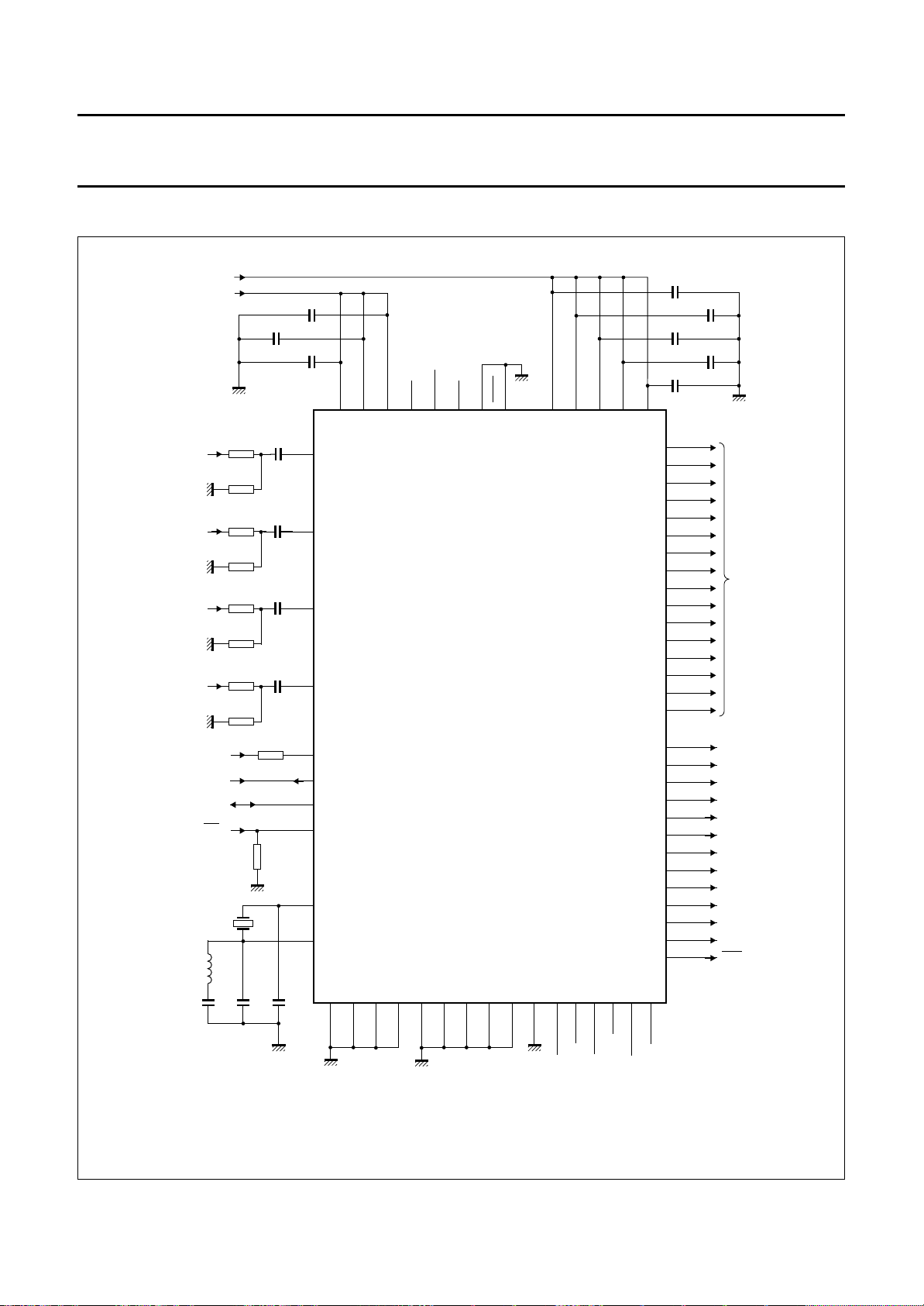
15 APPLICATION INFORMATION
handbook, full pagewidth
Q1(24.576 MHz)
AI22
V
AI21
V
AI12
V
AI11
V
L1
V
V
SSA
SSA
SSA
SSA
V
DDD
SCL
SDA
FEI
V
DDA
SSA
C16
1 nF
DD
10
µH
R10
27 Ω
R4
47 Ω
R9
27 Ω
R3
47 Ω
R8
27 Ω
R2
47 Ω
R7
27 Ω
R1
47 Ω
R6
100 nF
1 kΩ
C17
10 pF
C8
C4
22 nF
C3
22 nF
C2
22 nF
C1
22 nF
R5
1 kΩ
V
SS
100 nF
100 nF
XTAL
XTALI
C18
10 pF
V
SS
C9
C7
15 (6)
17 (8)
19 (10)
21 (12)
33 (24)
6 (63)
5 (62)
63 (52)
65 (54)
66 (55)
(16)
25
SSA0
V
DDA0VDDA1VDDA2
V
20
24
(11)
(15)
(9)
V
V
18
SSA1
SSA
(7)
(5)
14
SSA2
V
16
(13)
22
SS
V
n.c.
n.c.
TMS
TDI
13
12
(4)
(3)
(40)
(56)
51
67
SS1VSS2VSS3
V
V
SS
BST
n.c.
TDO
TCK
2
11
(59)
(2)
SAA7111A
(26)
(32)
35
43
SS4VSS5
V
TRST
1
(58)
(19)
28
V
SS
DD1VDD2VDD3VDD4VDD5
V
68
52
(57)
(41)
(61)
(64)
4
7
IICSA
SS
n.c.
n.c.
V
C15
C14
100 nF
C13
100 nF
C12
100 nF
C11
100 nF
VPO(15 : 0)
HREF
VREF
HS
VS
RTCO
RTS1
RTS0
GPSW
AOUT
LLC
LLC2
CREF
RES
V
SS
100 nF
27
34
44
(18)
(25)
(33)
(1)
10
8
9
DDI2C
V
n.c.
n.c.
(34) 45
(35) 46
(36) 47
(37) 48
(38) 49
(39) 50
(42) 53
(43) 54
(44) 55
(45) 56
(46) 57
(47) 58
(48) 59
(49) 60
(50) 61
(51) 62
(31) 42
(17) 26
(27) 38
(30) 41
(60) 3
(28) 39
(29) 40
(53) 64
(14) 23
(20) 29
(21) 30
(22) 31
(23) 32
37
36
n.c.
15
14
13
12
11
10
9
8
7
6
5
4
3
2
1
0
MGG071
The pin numbers given in parenthesis refer to the 64-pin package.
1996 Nov 07 38
Fig.31 Application diagram.
Page 39
Philips Semiconductors Preliminary specification
Enhanced Video Input Processor (EVIP) SAA7111A
handbook, full pagewidth
VPO
(15 : 8)
VPO
(7 : 0)
SAA7111A
(34) 45
(35) 46
(36) 47
(37) 48
(38) 49
(39) 50
(42) 53
(43) 54
(44) 55
(45) 56
(46) 57
(47) 58
(48) 59
(49) 60
(50) 61
(51) 62
(31) 42
(17) 26
(27) 38
(30) 41
(60) 3
(28) 39
(29) 40
(53) 64
(14) 23
(20) 29
(21) 30
(32) 31
(23) 32
15
14
13
12
11
10
9
8
7
6
5
4
3
2
1
0
VPO (15 : 11) R (7 : 3)
3
VPO (10 : 8)
3
VPO (7 : 5)
3
V
V
HREF
VREF
HS
VS
RTCO
RTS1
RTS0
GPSW
AOUT
LLC
CREF
RES
SS
SS
OEN
D7
D6
D5
D4
D3
D2
D1
D0
V
LLC2
SS
74HCT574
e.g.
V
CLK
5
DDVDD
O7
O6
O5
O4
O3
O2
O1
00
G (7 : 5)
G (4 : 2)
R (2 : 0)
3
G (1 : 0)
2
B (2 : 0)
3
B (7 : 3)VPO (4 : 0)
e.g. 74HCT240
R (7 : 0)
8
G (7 : 0)
8
B (7 : 0)
8
LLC2N
MGG073
The pin numbers given in parenthesis refer to the QFP64 package.
I2C-bus control bits:
OFTS(1 : 0) = 00 (subaddress 10H, bits D7 and D6).
RGB888 = 1 (subaddress 12H, bit D3).
1996 Nov 07 39
Fig.32 Application diagram for RGB 24-bit output format.
Page 40
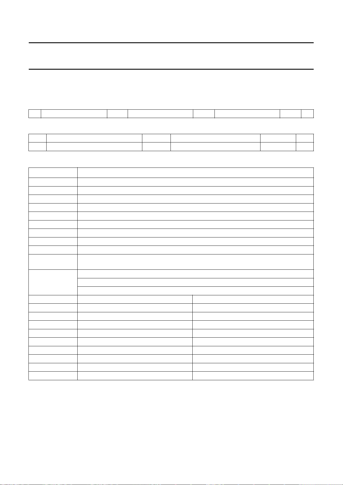
Philips Semiconductors Preliminary specification
Enhanced Video Input Processor (EVIP) SAA7111A
16 I2C-BUS DESCRIPTION
2
16.1 I
Table 6 Write procedure
Table 7 Read procedure (combined format)
Table 8 Description of I
S START condition
Sr repeated START condition
Slave address W 0100 1000b (IICSA = LOW) or 0100 1010b (IICSA = HIGH)
Slave address R 0100 1001b (IICSA = LOW) or 0100 1011b (IICSA = HIGH)
ACK s acknowledge generated by the slave
ACK m acknowledge generated by the master
Subaddress subaddress byte, see Table 9
Data data byte, see Table 9; note 1
P STOP condition
X = LSB slave
address
Slave address read = 49h or 4Bh; note 2
Subaddresses 00h chip version read and write; note 3
C-bus format
S SLAVE ADDRESS W ACK s SUBADDRESS ACK s DATA (N BYTES) ACK s P
S SLAVE ADDRESS W ACK s SUBADDRESS ACK s
Sr SLAVE ADDRESS R ACK s DATA (N BYTES) ACK m P
2
C-bus format
CODE DESCRIPTION
read/write control bit; X = 0, order to write (the circuit is slave receiver); X = 1, order to read
(the circuit is slave transmitter)
write = 48h or 4Ah
IICSA = 0 or 1
01h reserved −
02h to 05h front-end part read and write
06h to 13h decoder part read and write
14h reserved −
15h to 17h decoder part read and write
18h to 19h reserved −
1Ah to 1Ch Line-21 text slicer part read only
1Dh to 1Eh reserved −
1Fh status byte read only
Notes
1. If more than one byte DATA is transmitted then the auto-increment of the subaddress is performed.
2. During slave transmitter mode the SCL-LOW period may be extended by pulling SCL to LOW (in accordance with
2
the I
C-bus specification).
3. The I2C-bus subaddress 00 has to be initialized with 0 before being read.
1996 Nov 07 40
Page 41
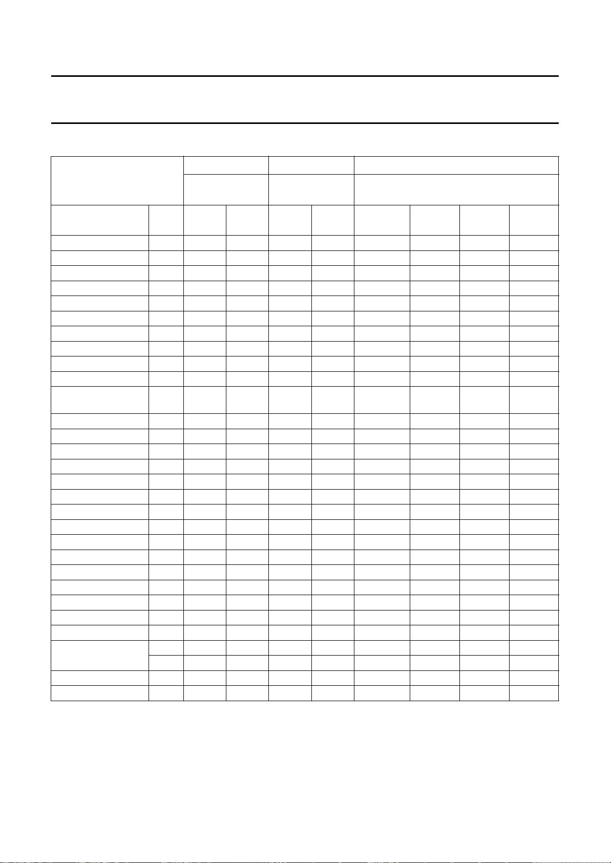
Philips Semiconductors Preliminary specification
Enhanced Video Input Processor (EVIP) SAA7111A
Table 9 I2C-bus receiver/transmitter overview
READ WRITE IICSA
SLAVE ADDRESS
49H
4BH
48H
4AH
0
1
REGISTER
FUNCTION
SUB-
ADDR
D7 D6 D5 D4 D3 D2 D1 D0
Chip version 00 ID07 ID06 ID05 ID04 ID03 ID02 ID01 ID00
Reserved 01
(1) (1) (1) (1) (1) (1) (1) (1)
Analog input contr 1 02 FUSE1 FUSE0 GUDL2 GUDL1 GUDL0 MODE2 MODE1 MODE0
(1)
Analog input contr 2 03
HLNRS VBSL WPOFF HOLDG GAFIX GAI28 GAI18
Analog input contr 3 04 GAI17 GAI16 GAI15 GAI14 GAI13 GAI12 GAI11 GAI10
Analog input contr 4 05 GAI27 GAI26 GAI25 GAI24 GAI23 GAI22 GAI21 GAI20
Horizontal sync start 06 HSB7 HSB6 HSB5 HSB4 HSB3 HSB2 HSB1 HSB0
Horizontal sync stop 07 HSS7 HSS6 HSS5 HSS4 HSS3 HSS2 HSS1 HSS0
Sync control 08 AUFD FSEL EXFIL
(1)
VTRC HPLL VNOI1 VNOI0
Luminance control 09 BYPS PREF BPSS1 BPSS0 VBLB UPTCV APER1 APER0
Luminance
0A BRIG7 BRIG6 BRIG5 BRIG4 BRIG3 BRIG2 BRIG1 BRIG0
brightness
Luminance contrast 0B CONT7 CONT6 CONT5 CONT4 CONT3 CONT2 CONT1 CONT0
Chroma saturation 0C SATN7 SATN6 SATN5 SATN4 SATN3 SATN2 SATN1 SATN0
Chroma Hue control 0D HUEC7 HUEC6 HUEC5 HUEC4 HUEC3 HUEC2 HUEC1 HUEC0
Chroma control 0E CDTO CSTD2 CSTD1 CSTD0 DCCF FCTC CHBW1 CHBW0
Reserved 0F
(1) (1) (1) (1) (1) (1) (1) (1)
Format/delay control 10 OFTS1 OFTS0 HDEL1 HDEL0 VRLN YDEL2 YDEL1 YDEL0
Output control 1 11 GPSW CM99 FECO COMPO OEYC OEHV VIPB COLO
Output control 2 12 RTSE1 RTSE0 TCLO CBR RGB888 DIT AOSL1 AOSL0
Output control 3 13 VCTR1 VCTR0 CCTR1 CCTR0 BCHI1 BCHI0 BCLO1 BCLO0
Reserved 14
(1) (1) (1) (1) (1) (1) (1) (1)
V_GATE1_START 15 VSTA7 VSTA6 VSTA5 VSTA4 VSTA3 VSTA2 VSTA1 VSTA0
V_GATE1_STOP 16 VSTO7 VSTO6 VSTO5 VSTO4 VSTO3 VSTO2 VSTO1 VSTO0
V_GATE1_MSB 17
Reserved 18-19
Text slicer status 1A
Decoded bytes of
the text slicer
1B P1 BYTE16 BYTE15 BYTE14 BYTE13 BYTE12 BYTE11 BYTE10
1C P2 BYTE26 BYTE25 BYTE24 BYTE23 BYTE22 BYTE21 BYTE20
Reserved 1D-1E
(1) (1) (1) (1) (1) (1)
(1) (1) (1) (1) (1) (1) (1) (1)
(1) (1) (1) (1)
(1) (1) (1) (1) (1) (1) (1) (1)
F2VAL F2RDY F1VAL F1RDY
VSTO8 VSTA8
Status byte 1F STTC HLCK FIDT GLIMT GLIMB WIPA SLTCA CODE
Note
1. All unused control bits must be programmed with logic 0.
1996 Nov 07 41
Page 42
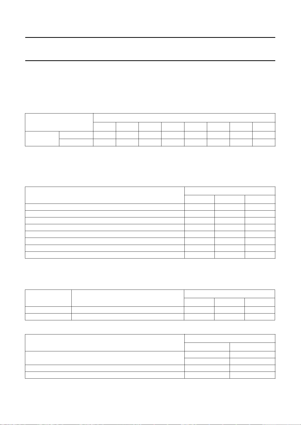
Philips Semiconductors Preliminary specification
Enhanced Video Input Processor (EVIP) SAA7111A
16.2 I2C-bus detail
The I2C-bus receiver slave address is 48H/49H. Subaddresses 0F, 14, 18, 19, 1D and 1E are reserved; subaddress 01
is reserved for chip version.
16.2.1 S
Table 10 Chip version SA00
Chip version
Note
1. X = reserved.
16.2.2 S
Table 11 Analog control 1 SA02
Mode 0: CVBS (automatic gain) 0 0 0
Mode 1: CVBS (automatic gain) 0 0 1
Mode 2: CVBS (automatic gain) 0 1 0
Mode 3: CVBS (automatic gain) 0 1 1
Mode 4: Y (automatic gain) + C (gain channel 2 fixed to GAI2 level) 1 0 0
Mode 5: Y (automatic gain) + C (gain channel 2 fixed to GAI2 level) 1 0 1
Mode 6: Y (automatic gain) + C (gain channel 2 adapted to Y gain) 1 1 0
Mode 7: Y (automatic gain) + C (gain channel 2 adapted to Y gain) 1 1 1
UBADDRESS 00
FUNCTION
UBADDRESS 02
LOGIC LEVELS
ID07 ID06 ID05 ID04 ID03 ID02 ID01 ID00
V1 0001XXXX
V2 0010XXXX
FUNCTION
(1)
CONTROL BITS D2 TO D0
MODE 2 MODE 1 MODE 0
Note
1. Mode select (see Figures 33 to 40).
Table 12 Analog control 1 SA 02, D5 to D3 (see Fig.14)
DECIMAL VALUE UPDATE HYSTERESIS FOR 9-BIT GAIN
0.... off 0 0 0
....7 ±7 LSB 1 1 1
Table 13 Analog control
ANALOG FUNCTION SELECT FUSE
Amplifier plus anti-alias filter bypassed 0 0
Amplifier active 1 0
Amplifier plus anti-alias filter active 1 1
1996 Nov 07 42
CONTROL BITS D5 TO D3
GUDL 2 GUDL 1 GUDL 0
CONTROL BITS D7 AND D6
FUSE 1 FUSE 0
01
Page 43
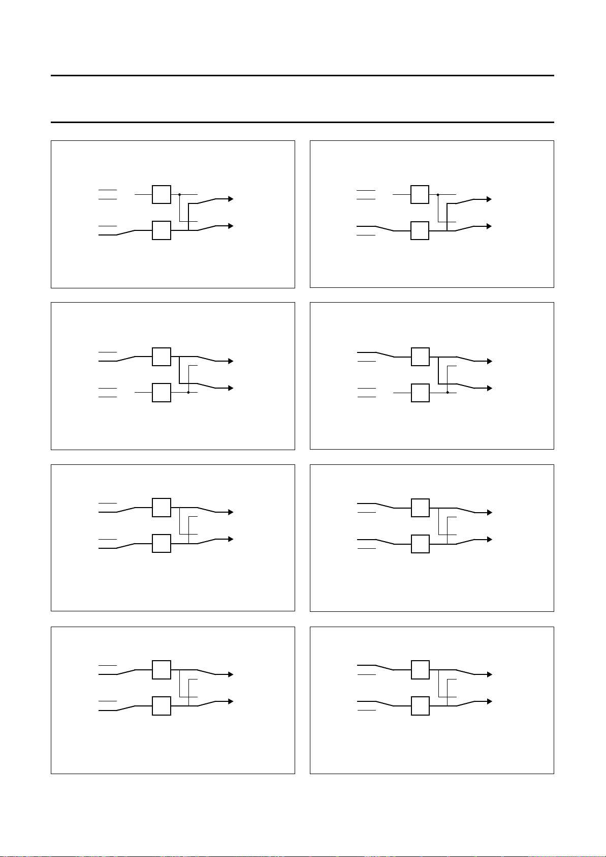
Philips Semiconductors Preliminary specification
Enhanced Video Input Processor (EVIP) SAA7111A
AI22
handbook, halfpage
AI21
AD2
CHROMA
AI22
handbook, halfpage
AI21
AD2
CHROMA
AI21
AI11
Fig.33 Mode 0; CVBS (automatic gain).
AI22
handbook, halfpage
AI21
AI12
AI11
Fig.35 Mode 2; CVBS (automatic gain).
AI22
handbook, halfpage
AI21
AD1
AD2
AD1
AD2
LUMA
MGC637
CHROMA
LUMA
MGC639
CHROMA
AI21
AI11
Fig.34 Mode 1; CVBS (automatic gain).
AI22
handbook, halfpage
AI21
AI12
AI11
Fig.36 Mode 3; CVBS (automatic gain).
AI22
handbook, halfpage
AI21
AD1
AD2
AD1
AD2
LUMA
MGC638
CHROMA
LUMA
MGC640
CHROMA
AI12
AI11
AD1
LUMA
MGC641
Fig.37 Mode 4 Y (automatic gain) + C
(gain channel 2 fixed to GAI2 level).
AI22
handbook, halfpage
AI21
AI12
AI11
AD2
AD1
CHROMA
LUMA
MGC643
Fig.39 Mode 6 Y (automatic gain) + C
(gain channel 2 adapted to Y gain).
1996 Nov 07 43
AI12
AI11
AD1
Fig.38 Mode 5 Y (automatic gain) + C
(gain channel 2 fixed to GAI2 level).
AI22
handbook, halfpage
AI21
AI12
AI11
AD2
AD1
Fig.40 Mode 7 Y (automatic gain) + C
(gain channel 2 adapted to Y gain).
LUMA
MGC642
CHROMA
LUMA
MGC644
Page 44
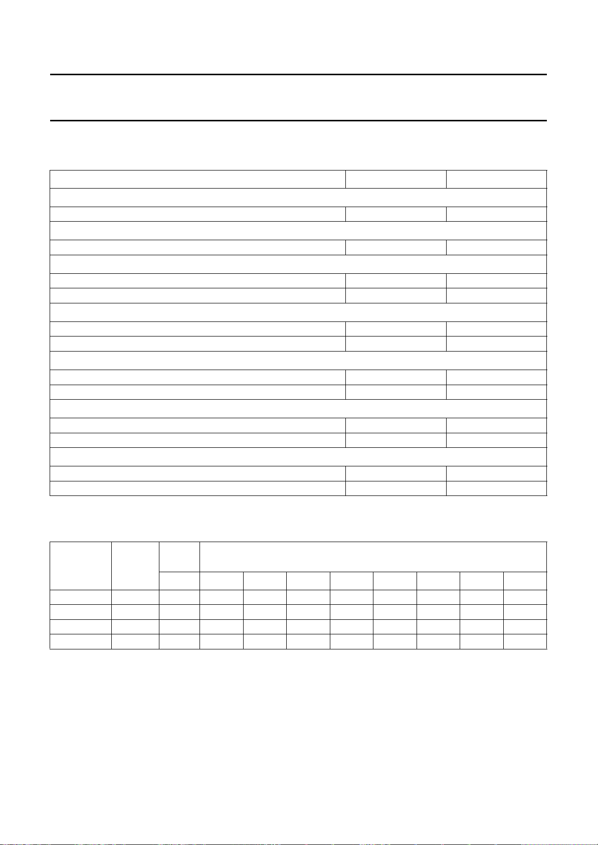
Philips Semiconductors Preliminary specification
Enhanced Video Input Processor (EVIP) SAA7111A
16.2.3 SUBADDRESS 03
Table 14 Analog control 2 (AICO2) SA03
FUNCTION LOGIC LEVEL DATA BIT
Static gain control channel 1 (GAI18) (see SA04)
Sign bit of gain control see Table 15 D0
Static gain control channel 2 (GAI28) (see SA05)
Sign bit of gain control see Table 16 D1
Gain control fix (GAFIX)
Automatic gain controlled by MODE 1 and MODE 0 0 D2
Gain control is user programmable via GAI1 + GAI2 1 D2
Automatic gain control integration (HOLDG)
AGC active 0 D3
AGC integration hold (freeze) 1 D3
White peak off (WPOFF)
White peak control active 0 D4
White peak off 1 D4
Vertical blanking select (VBSL)
Long vertical blanking 0 D5
Short vertical blanking 1 D5
HL not reference select (HLNRS)
Normal clamping by HL not 0 D6
Reference select by HL not 1 D6
16.2.4 S
Table 15 Gain control analog (AIC03); static gain control channel 1 GAI1 SA 04, D7 to D0
DECIMAL
UBADDRESS 04
GAIN
VALUE
0.... −5.98 0 0 0 000000
....255 0 0 1 1 111111
256.... 0 1 0 0 000000
....511 5.98 1 1 1 111111
(dB)
SIGN
BIT
GAI18 GAI17 GAI16 GAI15 GAI14 GAI13 GAI12 GAI11 GAI10
CONTROL BITS D7 TO D0
1996 Nov 07 44
Page 45
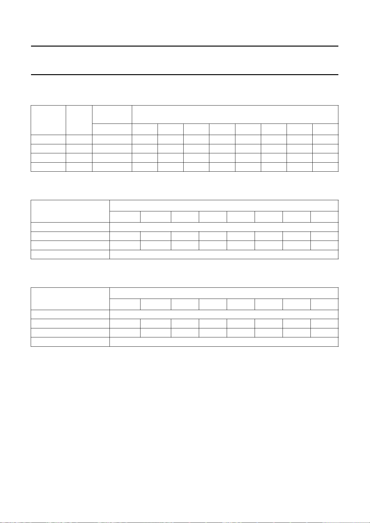
Philips Semiconductors Preliminary specification
Enhanced Video Input Processor (EVIP) SAA7111A
16.2.5 SUBADDRESS 05
Table 16 Gain control analog (AIC04); static gain control channel 2 GAI2 SA 05, D7 to D0
DECIMAL
VALUE
0.... −5.98 0 00000000
....255 0 0 11111111
256.... 0 1 00000000
....511 5.98 1 11111111
16.2.6 S
Table 17 Horizontal sync begin SA 06, D7 to D0
DELAY TIME
(STEP SIZE = 8/LLC)
16.2.7 S
Table 18 Horizontal sync stop SA 07, D7 to D0
GAIN
(dB)
UBADDRESS 06
−128...−108 forbidden (outside available central counter range)
−107... 1 0 0 1 0 1 0 1
...108 0 1 1 0 1 1 0 0
109...127 forbidden (outside available central counter range)
UBADDRESS 07
SIGN BIT
(SA 03, D1)
GAI28 GAI27 GAI26 GAI25 GAI24 GAI23 GAI22 GAI21 GAI20
HSB7 HSB6 HSB5 HSB4 HSB3 HSB2 HSB1 HSB0
CONTROL BITS D7 to D0
CONTROL BITS D7 to D0
DELAY TIME
(STEP SIZE = 8/LLC)
−128...−108 forbidden (outside available central counter range)
−107... 1 0 0 1 0 1 0 1
...108 0 1 1 0 1 1 0 0
109...127 forbidden (outside available central counter range)
HSS7 HSS6 HSS5 HSS4 HSS3 HSS2 HSS1 HSS0
CONTROL BITS D7 to D0
1996 Nov 07 45
Page 46
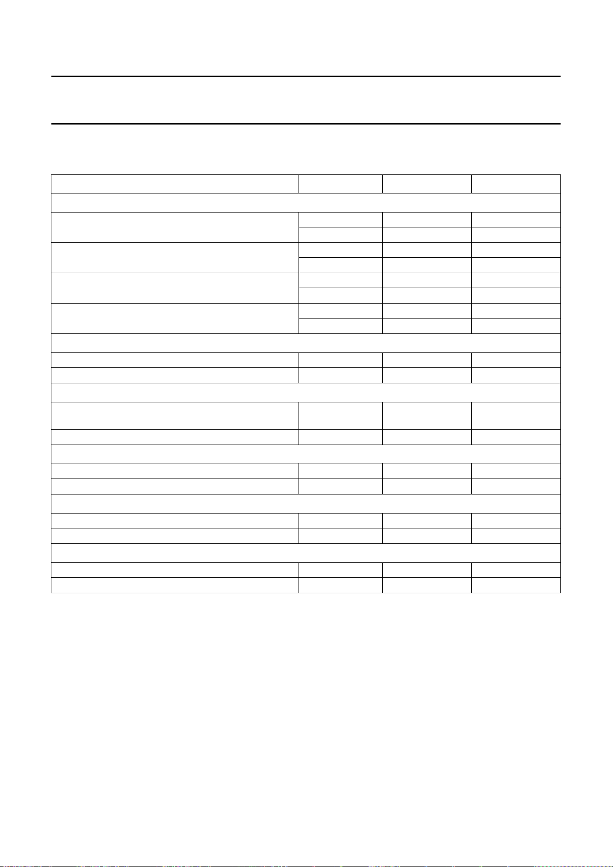
Philips Semiconductors Preliminary specification
Enhanced Video Input Processor (EVIP) SAA7111A
16.2.8 SUBADDRESS 08
Table 19 Sync control SA 08, D7 to D5, D3 to D0
FUNCTION VNOI BITS LOGIC LEVELS DATA BITS
Vertical noise reduction (VNOI)
Normal mode VNOI1 0 D1
VNOI0 0 D0
Searching mode VNOI1 0 D1
VNOI0 1 D0
Free running mode VNOI1 1 D1
VNOI0 0 D0
Vertical noise reduction bypassed VNOI1 1 D1
VNOI0 1 D0
Horizontal PLL (HPLL)
PLL closed HPLL 0 D2
PLL open, horizontal frequency fixed HPLL 1 D2
TV/VTR mode select (VTRC)
TV mode
(recommended for poor quality TV signals only)
VTR mode (recommended as default setting) VTRC 1 D3
Extended loop filter (EXFIL)
Word width of the loop filter (LF2) amplification = 16-bit EXFIL 0 D5
Word width of the loop filter (LF2) amplification = 14-bit EXFIL 1 D5
Field selection (FSEL)
50 Hz, 625 lines FSEL 0 D6
60 Hz, 525 lines FSEL 1 D6
Automatic field detection (AUFD)
Field state directly controlled via FSEL AUFD 0 D7
Automatic field detection AUFD 1 D7
VTRC 0 D3
1996 Nov 07 46
Page 47
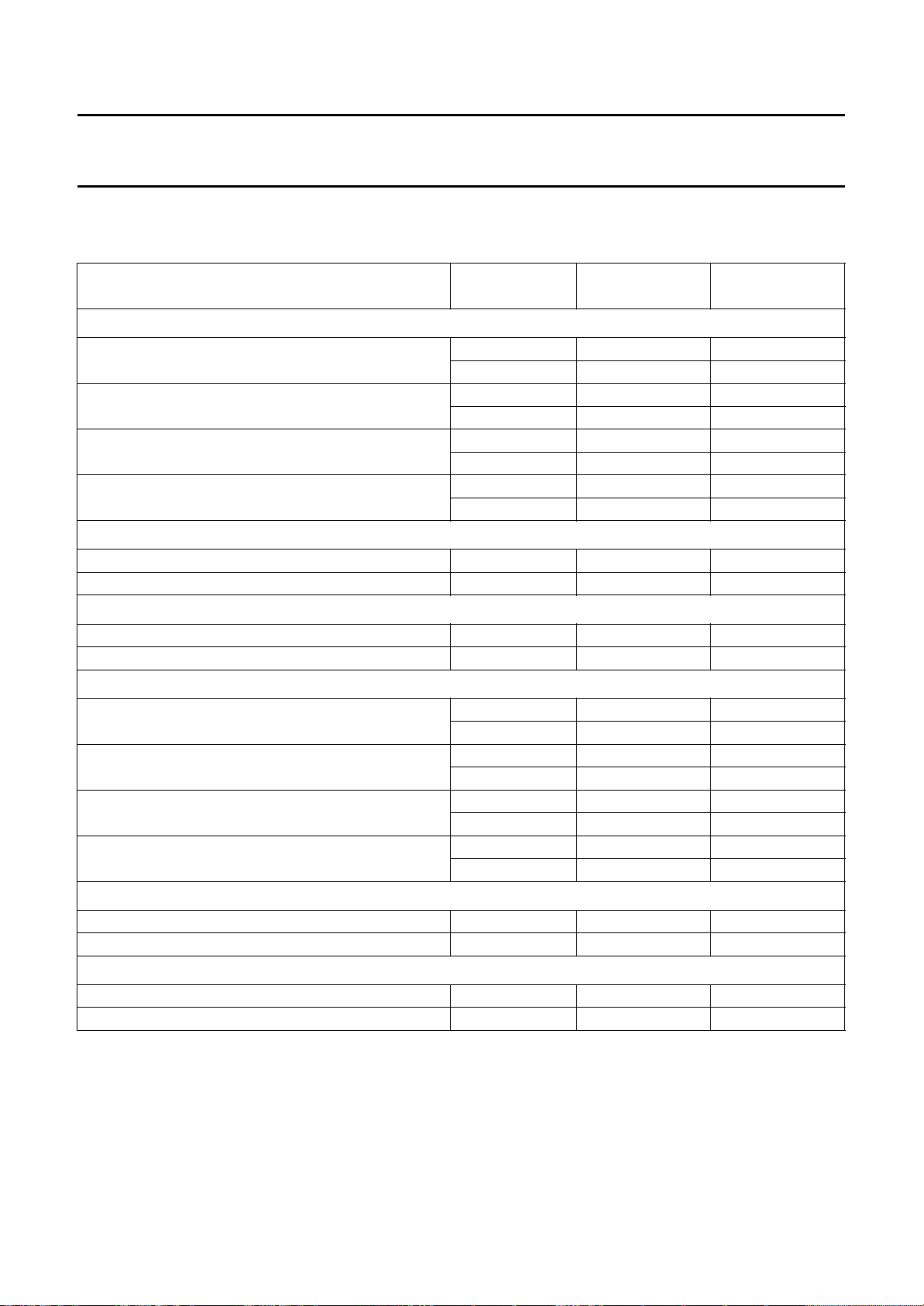
Philips Semiconductors Preliminary specification
Enhanced Video Input Processor (EVIP) SAA7111A
16.2.9 SUBADDRESS 09
Table 20 Luminance control SA 09, D7 to D0
FUNCTION
Aperture factor (APER)
Aperture factor = 0 APER1 0 D1
Aperture factor = 0.25 APER1 0 D1
Aperture factor = 0.5 APER1 1 D1
Aperture factor = 1.0 APER1 1 D1
Update time interval for AGC value (UPTCV)
Horizontal update (once per line) UPTCV 0 D2
Vertical update (once per field) UPTCV 1 D2
Vertical blanking luminance bypass (VBLB)
Active luminance processing VBLB 0 D3
Luminance bypass during vertical blanking VBLB 1 D3
Aperture band pass (centre frequency) (BPSS)
Centre frequency = 4.1 MHz BPSS1 0 D5
Centre frequency = 3.8 MHz; note 1 BPSS1 0 D5
Centre frequency = 2.6 MHz; note 1 BPSS1 1 D5
Centre frequency = 2.9 MHz; note 1 BPSS1 1 D5
APER/BPSS
BITS
APER0 0 D0
APER0 1 D0
APER0 0 D0
APER0 1 D0
BPSS0 0 D4
BPSS0 1 D4
BPSS0 0 D4
BPSS0 1 D4
LOGIC LEVELS DATA BITS
Prefilter active (PREF)
Bypassed PREF 0 D6
Active PREF 1 D6
Chrominance trap bypass (BYPS)
Chrominance trap active; default for CVBS mode BYPS 0 D7
Chrominance trap bypassed; default for S-Video mode BYPS 1 D7
Note
1. Not to be used with bypassed chrominance trap.
1996 Nov 07 47
Page 48
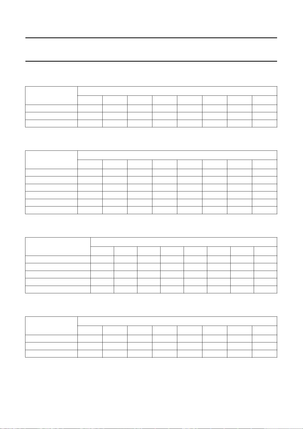
Philips Semiconductors Preliminary specification
Enhanced Video Input Processor (EVIP) SAA7111A
16.2.10 SUBADDRESS 0A
Table 21 Luminance brightness control BRIG7 to BRIG0 SA 0A
OFFSET
255 (bright) 1 1 1 1 1 1 1 1
128 (CCIR level) 1 0 0 0 0 0 0 0
0 (dark) 0 0 0 0 0 0 0 0
16.2.11 S
Table 22 Luminance contrast control CONT7 to CONT0 SA 0B
1.109 (CCIR level) 0 1 0 0 0 1 1 1
−1 (inverse luminance) 1 1 0 0 0 0 0 0
−2 (inverse luminance) 1 0 0 0 0 0 0 0
16.2.12 SUBADDRESS 0C
Table 23 Chrominance saturation control SATN7 to SATN0 SA 0C
UBADDRESS 0B
GAIN
1.999 (maximum) 0 1 1 1 1 1 1 1
1.0 01000000
0 (luminance off) 0 0 0 0 0 0 0 0
BRIG7 BRIG6 BRIG5 BRIG4 BRIG3 BRIG2 BRIG1 BRIG0
CONT7 CONT6 CONT5 CONT4 CONT3 CONT2 CONT1 CONT0
CONTROL BITS D7 to D0
CONTROL BITS D7 to D0
GAIN
1.999 (maximum) 0 1 1 1 1 1 1 1
1.0 (CCIR level) 0 1 0 0 0 0 0 0
0 (colour off) 0 0 0 0 0 0 0 0
−1 (inverse chrominance) 1 1 0 0 0 0 0 0
−2 (inverse chrominance) 1 0 0 0 0 0 0 0
16.2.13 S
Table 24 Chrominance hue control HUEC7 to HUEC0 SA 0D
HUE PHASE (DEG)
UBADDRESS 0D
+178.6.... 0 1 1 1 1 1 1 1
....0.... 0 0 0 0 0 0 0 0
....−180 10000000
SATN7 SATN6 SATN5 SATN4 SATN3 SATN2 SATN1 SATN0
HUEC7 HUEC6 HUEC5 HUEC4 HUEC3 HUEC2 HUEC1 HUEC0
CONTROL BITS D7 to D0
CONTROL BITS D7 to D0
1996 Nov 07 48
Page 49
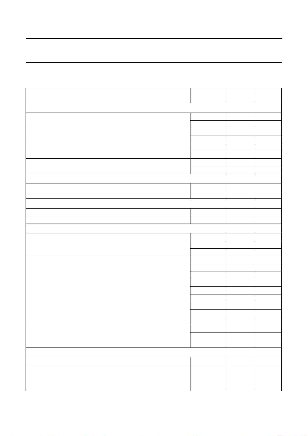
Philips Semiconductors Preliminary specification
Enhanced Video Input Processor (EVIP) SAA7111A
16.2.14 SUBADDRESS 0E
Table 25 Chrominance control SA 0E
FUNCTION
Chroma bandwidth (CHBW0 and CHBW1)
Small bandwidth (≈ 620 kHz) CHBW1 0 D1
Nominal bandwidth (≈ 800 kHz) CHBW1 0 D1
Medium bandwidth (≈ 920 kHz) CHBW1 1 D1
Wide bandwidth (≈ 1000 kHz) CHBW1 1 D1
Fast colour time constant (FCTC)
Nominal time constant FCTC 0 D2
Fast time constant FCTC 1 D2
Disable chrominance comb filter (DCCF)
Chrominance comb filter on (during VREF = 1) (see Figs 24 and 25) DCCF 0 D3
Chrominance comb filter off DCCF 1 D3
Colour standard (CSTD0 to CSTD2); logic levels 100, 110 and 111 are reserved, do not use
Colour standard control automatic switching between PAL BGHI and
NTSC M (NTSC-Japan with special level adjustment; luminance brightness
subaddress 0A = 95H, luminance contrast subaddress 0BH = 48H)
Colour standard control automatic switching between NTSC 4.43 (50 Hz)
and PAL 4.43 (60 Hz)
Colour standard control automatic switching between PAL N and
NTSC 4.43 (60 Hz)
Colour standard control automatic switching between NTSC N and PAL M CSTD2 0 D6
Colour standard control automatic switching between SECAM and
PAL 4.43 (60 Hz)
CHBW/CSTD
BITS
CHBW0 0 D0
CHBW0 1 D0
CHBW0 0 D0
CHBW0 1 D0
CSTD2 0 D6
CSTD1 0 D5
CSTD0 0 D4
CSTD2 0 D6
CSTD1 0 D5
CSTD0 1 D4
CSTD2 0 D6
CSTD1 1 D5
CSTD0 0 D4
CSTD1 1 D5
CSTD0 1 D4
CSTD2 1 D6
CSTD1 0 D5
CSTD0 1 D4
LOGIC
LEVELS
DATA
BITS
Clear DTO (CDTO)
Disabled CDTO 0 D7
Every time CDTO is set, the internal subcarrier DTO phase is reset to 0°
and the RTCO output generates a logic 0 at time slot 68 (see RTCO
description Fig.20). So an identical subcarrier phase can be generated by
an external device (e.g. an encoder).
1996 Nov 07 49
CDTO 1 D7
Page 50
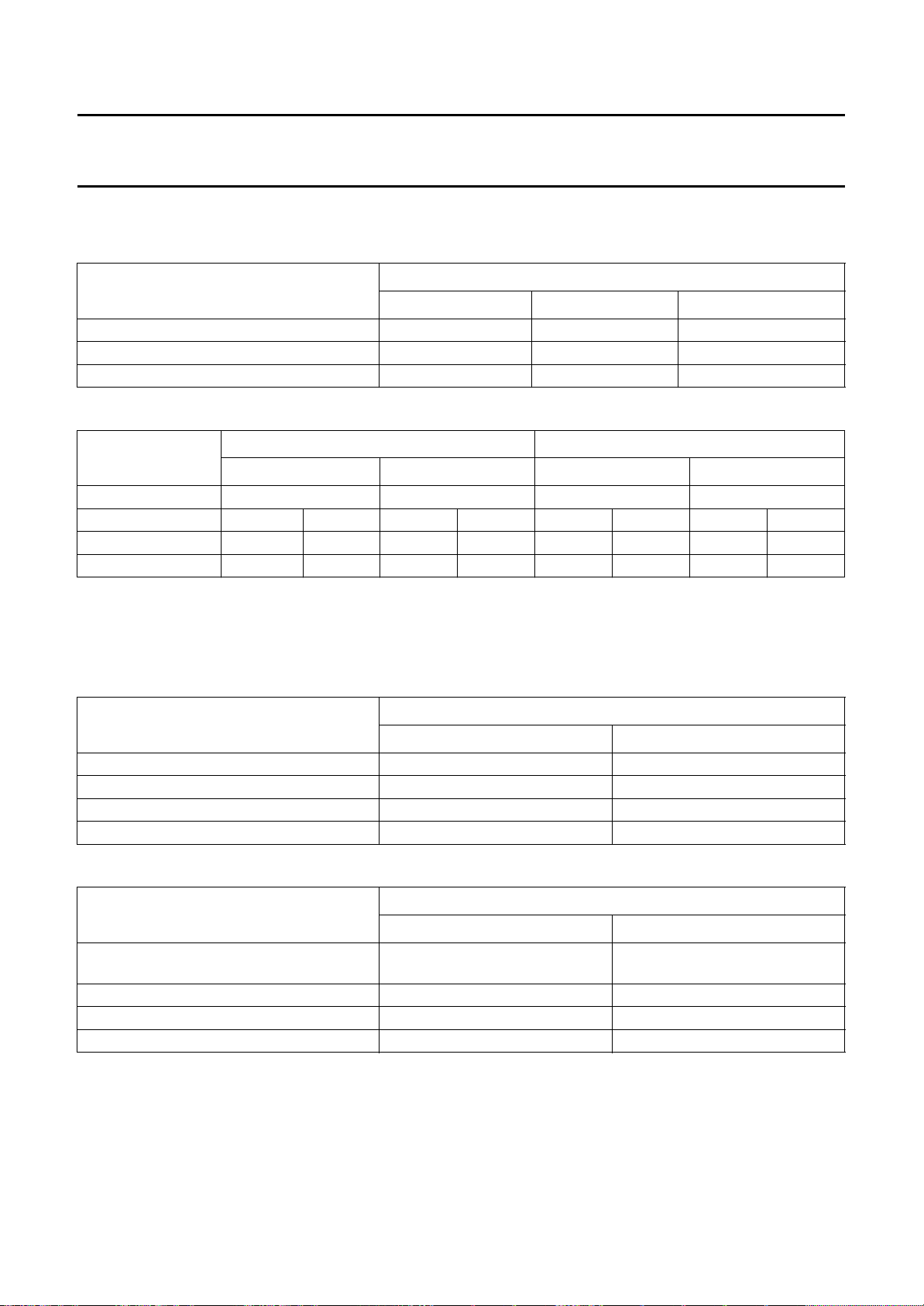
Philips Semiconductors Preliminary specification
Enhanced Video Input Processor (EVIP) SAA7111A
16.2.15 SUBADDRESS 10
Table 26 Format/delay control SA 10
LUMINANCE DELAY COMPENSATION
(STEPS IN 2/LLC)
YDEL2 YDEL1 YDEL0
CONTROL BITS D2 to D0
−4... 1 0 0
...0... 0 0 0
...3 0 1 1
Table 27 VREF pulse position and length VRLN SA 10 (D3)
VREF at 60 Hz 525 LINES
(2)
VREF at 50 Hz 625 LINES
(2)
VRLN
0101
Length 240 242 286 288
Line number first last first last first last first last
Field 1
Field 2
(1)
(1)
19 (22) 258 (261) 18 (21) 259 (262) 24 309 23 310
282 (285) 521 (524) 281 (284) 522 (525) 337 622 336 623
Notes
1. The numbers given in parenthesis refer to CCIR line counting.
2. Additional VREF positions can be achieved via I
2
C-bus bits VCTR1 and VCTR0 (see Fig.7).
Table 28 Fine position of HS HDEL0 and HDEL1 SA 10
FINE POSITION OF HS WITH A STEP SIZE
OF 2/LLC
HDEL1 HDEL0
CONTROL BITS D5 and D4
000
101
210
311
Table 29 Output format selection OFTS0 and OFTS1 SA 10
FORMATS
RGB (5, 6, 5), RGB (8, 8, 8) (dependent on
control bit RGB888) see Table 31
YUV 422 16 bits 0 1
YUV 411 12 bits 1 0
YUV CCIR-656 8 bits 1 1
1996 Nov 07 50
CONTROL BITS D7 and D6
OFTS1 OFTS0
00
Page 51
Philips Semiconductors Preliminary specification
Enhanced Video Input Processor (EVIP) SAA7111A
16.2.16 SUBADDRESS 11
Table 30 Output control 1 SA 11
FUNCTION BITS LOGIC LEVELS DATA BIT
Colour on (COLO)
Automatic colour killer COLO 0 D0
Colour forced on COLO 1 D0
Decoder VIP bypassed (VIPB)
DMSD data to YUV output VIPB 0 D1
ADC data to YUV output; dependent on mode
settings
Output enable horizontal/vertical sync (OEHV)
HS, HREF, VREF and VS high-impedance inputs OEHV 0 D2
Outputs HS, HREF, VREF and VS active OEHV 1 D2
VIPB 1 D1
Output enable YUV data (OEYC)
VPO-bus high-impedance inputs OEYC 0 D3
Output VPO-bus active OEYC 1 D3
Inverse composite blank (COMPO)
VREF is vertical reference COMPO 0 D4
VREF is inverse composite blank COMPO 1 D4
FEI control (FECO)
FEI sampling at CREF = LOW
(SAA7110 compatible; (see Fig.19)
FEI sampling at CREF = HIGH FECO 1 D5
CM99 compatibility to SAA7199 (CM99)
Default value CM99 0 D6
To be set if SAA7199 (digital encoder) is used for
re-encoding in conjunction with RTCO
General purpose switch (GPSW)
Switches directly pin 64 GPSW GPSW 0 D7
FECO 0 D5
CM99 1 D6
GPSW 1 D7
1996 Nov 07 51
Page 52
Philips Semiconductors Preliminary specification
Enhanced Video Input Processor (EVIP) SAA7111A
16.2.17 SUBADDRESS 12
Table 31 Output control 2 SA 12, D7 to D6, D4 to D0
FUNCTION AOSL BITS LOGIC LEVELS DATA BITS
Analog test select (AOSL)
AOUT connected to internal test point 1 AOSL1 0 D1
AOSL0 0 D0
AOUT connected to input AD1 AOSL1 0 D1
AOSL0 1 D0
AOUT connected to input AD2 AOSL1 1 D1
AOSL0 0 D0
AOUT connected to internal test point 2 AOSL1 1 D1
AOSL0 1 D0
Dithering (noise shaping) control (DIT)
Dithering off DIT 0 D2
Dithering on DIT 1 D2
RGB output format selection (RGB888)
RGB (5, 6, 5) RGB888 0 D3
RGB (8, 8, 8) RGB888 1 D3
Chrominance interpolation filter function (CBR)
Cubic interpolation (default) CBR 0 D4
Linear interpolation (lower bandwidth) CBR 1 D4
3-state control VPO7 to VPO0 (TCLO)
VPO7 to VPO0 depends on OEYC,
(default)
VPO7 to VPO0 in 3-state
[and OFTS (1 : 0) = 3]
Real time outputs mode select (RTSE0)
ODD switched to output pin 40 RTSE0 0 D6
VL switched to output pin 40 RTSE0 1 D6
Real time outputs mode select (RTSE1)
PLIN switched to output pin 39 RTSE1 0 D7
HL switched to output pin 39 RTSE1 1 D7
FEI only
TCLO 0 D5
TCLO 1 D5
1996 Nov 07 52
Page 53
Philips Semiconductors Preliminary specification
Enhanced Video Input Processor (EVIP) SAA7111A
16.2.18 SUBADDRESS 13
Table 32 Output control 3 SA 13
FUNCTION BITS LOGIC LEVELS DATA BITS
Bypass control LOW for VPO7 to VPO0
No bypass BCLO1 0 D1
BCLO0 0 D0
Permanent bypass BCLO1 0 D1
BCLO0 1 D0
Bypass controlled by V_GATE BCLO1 1 D1
BCLO0 0 D0
Bypass controlled by delayed V_GATE BCLO1 1 D1
BCLO0 1 D0
Bypass control HIGH for VPO15 to VPO8
No bypass BCHI1 0 D3
BCHI0 0 D2
Permanent bypass BCHI1 0 D3
BCHI0 1 D2
Bypass controlled by V_GATE BCHI1 1 D3
BCHI0 0 D2
Bypass controlled by delayed V_GATE BCHI1 1 D3
BCHI0 1 D2
Clock Reference Output Control
CREF is independent of VREF CCTR1 0 D5
CCTR0 0 D4
CREF is LOW if VREF = 0 CCTR1 0 D5
CCTR0 1 D4
CREF is HIGH if VREF = 0 CCTR1 1 D5
CCTR0 0 D4
CREF always = 1 CCTR1 1 D5
CCTR0 1 D4
Vertical Reference Output Control (VREF)
Internal VREF VCTR1 0 D7
VCTR0 0 D6
VREF_CCIR VCTR1 0 D7
VCTR0 1 D6
Programmable V_GATE VCTR1 1 D7
VCTR0 0 D6
Delayed programmable V_GATE VCTR1 1 D7
VCTR0 1 D6
1996 Nov 07 53
Page 54
Philips Semiconductors Preliminary specification
Enhanced Video Input Processor (EVIP) SAA7111A
16.2.19 SUBADDRESS 15
Table 33 Start of decoded data on VPO-port SA 15; note 1
Frame
line
FIELD
50 Hz 1st 1 312 1 0 0 1 1 1 0 0 0
60 Hz 1st 1 (4) 262 1 0 0 0 0 0 1 1 0
Notes
1. Start of decoded data on VPO-port (end of bypassed region; start of VREF if selected by VCTR1 and VCTR0).
2. Line numbers in brackets refer to CCIR line counting.
counting
2nd 314
1st 2 0.... 0 0 0 0 0 0 0 0 0
2nd 315
1st 312 ....310 1 0 0 1 1 0 1 1 1
2nd 625
2nd 264 (267)
1st 2 (5) 0.... 0 0 0 0 0 0 0 0 0
2nd 265 (268)
1st 262 (265) ....260 1 0 0 0 0 0 1 0 1
2nd 525 (3)
(2)
Decimal
value
MSB
(SA 17, D0)
VSTA8
CONTROL BITS D7 to D0
VSTA7VSTA6VSTA5VSTA4VSTA3VSTA2VSTA1VSTA
0
1996 Nov 07 54
Page 55
Philips Semiconductors Preliminary specification
Enhanced Video Input Processor (EVIP) SAA7111A
16.2.20 SUBADDRESS 16
Table 34 Start of decoded data on VPO-port SA 16; note 1
Frame
line
FIELD
50Hz1st1 312 1 00111000
60Hz1st1(4)262 1 00000110
Notes
1. Start of decoded data on VPO-port (begin of bypassed region; stop of VREF if selected by VCTR1 and VCTR0).
2. Line numbers in brackets refer to CCIR line counting.
counting
2nd 314
1st 2 0.... 0 0 0 0 00000
2nd 315
1st 312 ....310 1 0 0 1 10111
2nd 625
2nd 264 (267)
1st 2 (5) 0.... 0 0 0 0 00000
2nd 265 (268)
1st 262 (265) ....260 1 0 0 0 00101
2nd 525 (3)
(2)
Decimal
value
MSB
(SA 17, D0)
VSTO8
CONTROL BITS D7 to D0
VSTO7VSTO6VSTO5VSTO4VSTO3VSTO2VSTO1VSTO
0
16.2.21 S
Table 35 Sign bits of the VBI-data stream control
VBI-data stream start (VSTA8); see SA 15
Sign bit VBI-data stream start see Table 33 D0
VBI-data stream stop (VSTA8); see SA 16
Sign bit VBI-data stream stop see Table 34 D1
UBADDRESS 17
FUNCTION LOGIC LEVELS CONTROL BITS
1996 Nov 07 55
Page 56
Philips Semiconductors Preliminary specification
Enhanced Video Input Processor (EVIP) SAA7111A
16.2.22 SUBADDRESS 1A (READ-ONLY REGISTER)
Table 36 Line-21 text slicer status SA 1A, D3 to D0
2
I
C-BUS
CONTROL BITS
F1RDY new data on field 1 has been acquired (for asynchronous reading); active HIGH D0
F1VAL Line-21 of field 1 carries valid data; active HIGH D1
F2RDY new data on field 2 has been acquired (for asynchronous reading); active HIGH D2
F2VAL Line-21 of field 2 carries valid data; active HIGH D3
FUNCTION DATA BIT
16.2.23 S
UBADDRESS 1B (READ-ONLY REGISTER)
Table 37 First decoded data byte of the text slicer SA 1B
2
C-BUS
I
CONTROL BITS
FUNCTION DATA BIT
BYTE1 (6 to 0) data bit 6 to 0 of first data byte D6 to D0
P1 parity error flag bit; bit goes HIGH when a parity error has occurred D7
16.2.24 S
UBADDRESS 1C (READ-ONLY REGISTER)
Table 38 Second decoded data byte of the text slicer SA 1C
I2C-BUS
CONTROL BITS
FUNCTION DATA BIT
BYTE2 (6 to 0) data bit 6 to 0 of second data byte D6 to D0
P2 parity error flag bit; bit goes HIGH when a parity error has occurred D7
16.2.25 SUBADDRESS 1F (READ-ONLY REGISTER)
Table 39 Status byte SA 1F
2
C-BUS
I
CONTROL BITS
FUNCTION DATA BIT
CODE colour signal in accordance with selected standard has been detected; active HIGH D0
SLTCA slow time constant active in WIPA-mode; active HIGH D1
WIPA white peak loop is activated; active HIGH D2
GLIMB gain value for active luminance channel is limited [min (bottom)]; active HIGH D3
GLIMT gain value for active luminance channel is limited [max (top)]; active HIGH D4
FIDT identification bit for detected field frequency; LOW = 50 Hz, HIGH = 60 Hz D5
HLCK status bit for locked horizontal frequency; LOW = locked, HIGH = unlocked D6
STTC status bit for horizontal phase loop; LOW = TV time-constant,
HIGH = VTR time-constant
D7
1996 Nov 07 56
Page 57
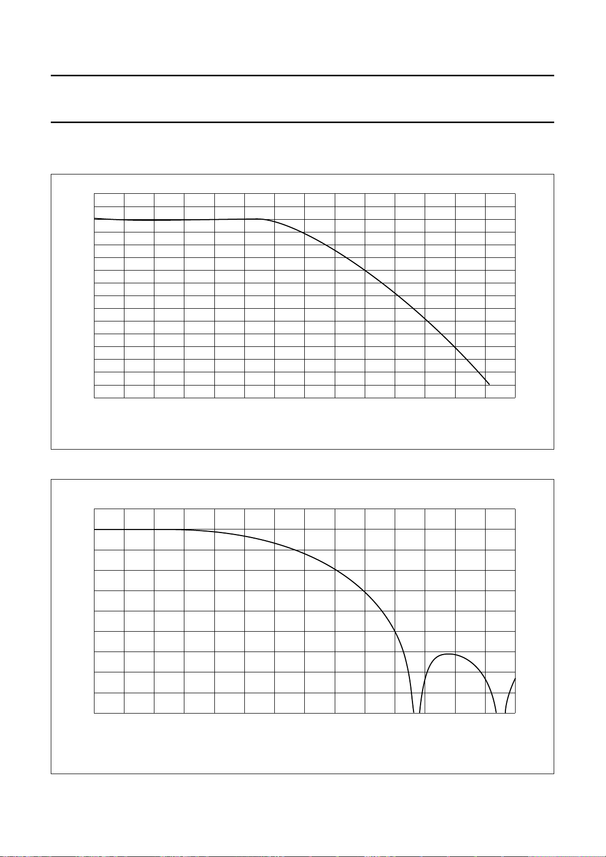
Philips Semiconductors Preliminary specification
Enhanced Video Input Processor (EVIP) SAA7111A
17 FILTER CURVES
17.1 Anti-alias filter curve
handbook, full pagewidth
6
V
(dB)
0
−6
−12
−18
−24
−30
−36
−42
024 68101214
17.2 TUF-block filter curve
MGD138
f (MHz)
Fig.41 Anti-alias filter.
6
V
handbook, full pagewidth
(dB)
0
−6
−12
−18
−24
−30
−36
−42
−48
−54
024 68101214
Fig.42 Interpolation filter for the upsampled CVBS-signal.
1996 Nov 07 57
MGG067
f (MHz)
Page 58
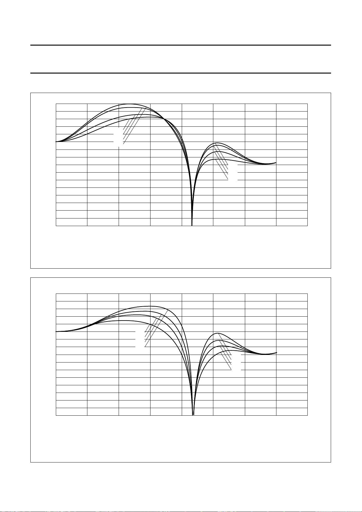
Philips Semiconductors Preliminary specification
Enhanced Video Input Processor (EVIP) SAA7111A
17.3 Luminance filter curves
18
handbook, full pagewidth
V
Y
(dB)
6
−6
−18
−30
024 86
(1) = 43H; (2) = 53H; (3) = 63H; (4) = 73H.
(1)
(2)
(4)
(3)
(1)
(2)
(4)
(3)
f
Y (MHz)
MGD139
Fig.43 Luminance control SA 09H, 4.43 MHz Trap/CVBS mode, prefilter on, different aperture bandpass centre
frequencies.
18
handbook, full pagewidth
V
Y
(dB)
6
−6
−18
−30
024 86
(1) = 40H; (2) = 41H; (3) = 42H; (4) = 43H.
Fig.44 Luminance control SA 09H, 4.43 MHz Trap/CVBS mode, prefilter on, different aperture factors.
(1)
(2)
(3)
(4)
(4)
(3)
(2)
(1)
f
Y (MHz)
MGD140
1996 Nov 07 58
Page 59
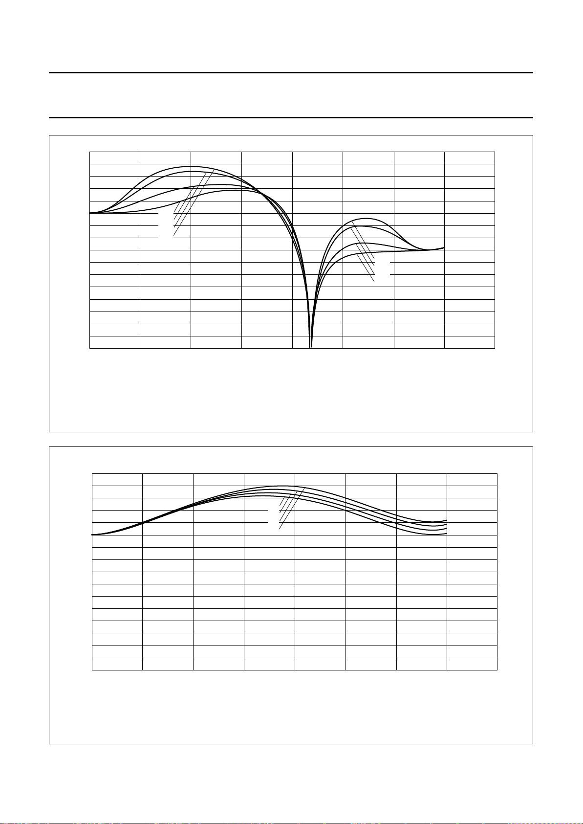
Philips Semiconductors Preliminary specification
Enhanced Video Input Processor (EVIP) SAA7111A
18
handbook, full pagewidth
V
Y
(dB)
6
(1)
(2)
(4)
(3)
−6
−18
−30
024 86
(1) = 03H; (2) = 13H; (3) = 23H; (4) = 33H.
(1)
(2)
(4)
(3)
f
Y (MHz)
MGD141
Fig.45 Luminance control SA 09H, 4.43 MHz Trap/CVBS mode, prefilter off, different aperture band-pass centre
frequencies.
18
handbook, full pagewidth
V
Y
(dB)
6
−6
−18
−30
024 86
(1) = C0H; (2) = C1H; (3) = C2H; (4) = C3H.
Fig.46 Luminance control SA 09H, Y/C mode, prefilter on, different aperture factors.
(1)
(2)
(3)
(4)
f
Y (MHz)
MGD142
1996 Nov 07 59
Page 60
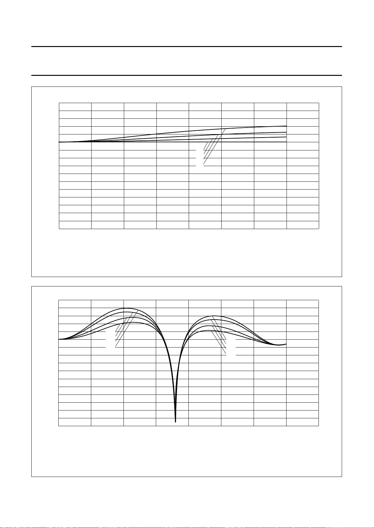
Philips Semiconductors Preliminary specification
Enhanced Video Input Processor (EVIP) SAA7111A
18
handbook, full pagewidth
V
Y
(dB)
6
−6
−18
−30
024 86
(1) = 80H; (2) = 81H; (3) = 82H; (4) = 83H.
Fig.47 Luminance control SA 09H, Y/C mode, prefilter off, different aperture factors.
(1)
(2)
(3)
(4)
f
Y (MHz)
MGD143
18
handbook, full pagewidth
V
Y
(dB)
6
−6
−18
−30
024 86
(1) = 43H; (2) = 53H; (3) = 63H; (4) = 73H.
(1)
(2)
(4)
(3)
(1)
(2)
(4)
(3)
f
Y (MHz)
MGD144
Fig.48 Luminance control SA 09H, 3.58 MHz Trap/CVBS mode, prefilter on, different aperture band-pass centre
frequencies.
1996 Nov 07 60
Page 61
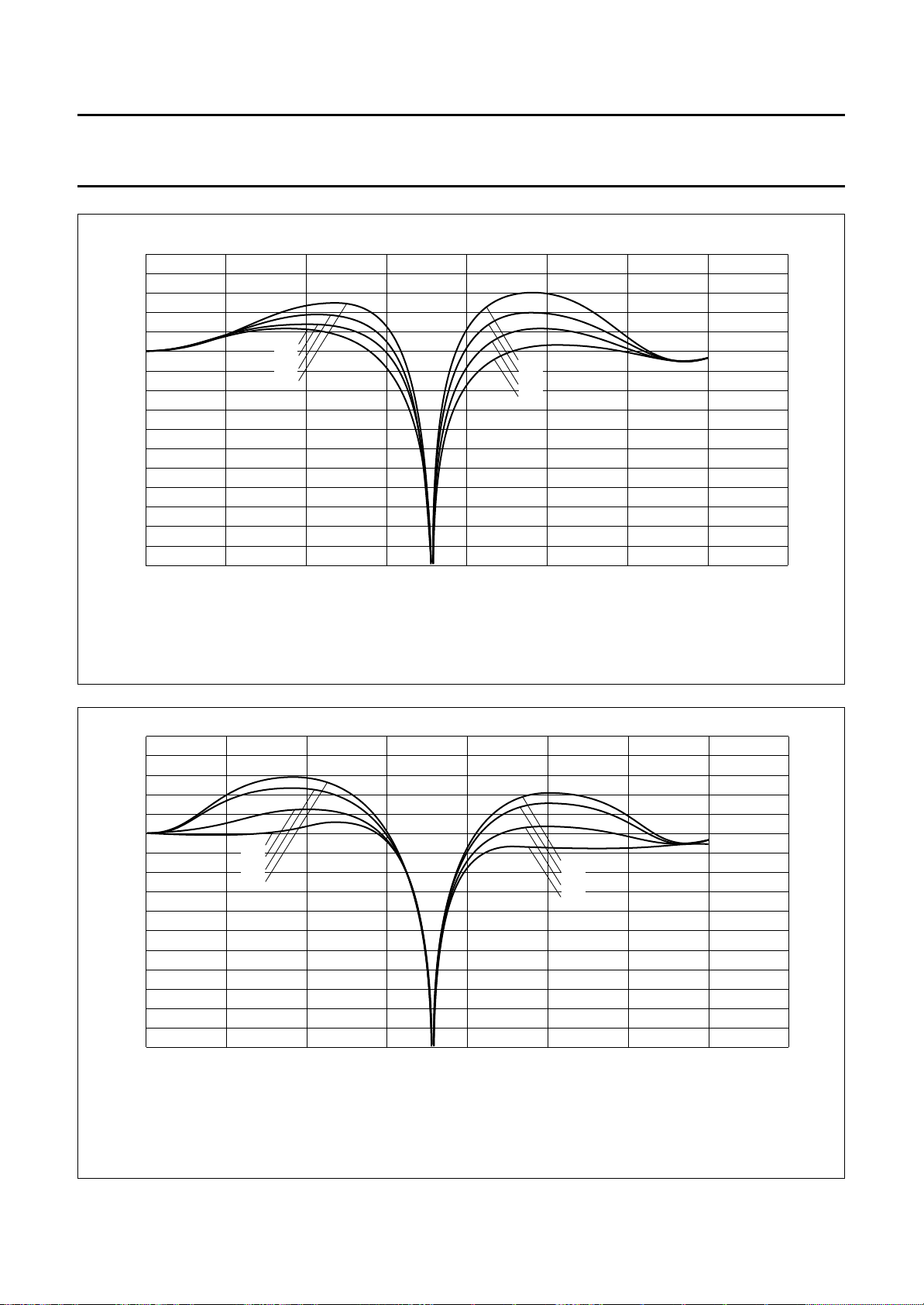
Philips Semiconductors Preliminary specification
Enhanced Video Input Processor (EVIP) SAA7111A
18
handbook, full pagewidth
V
Y
(dB)
6
−6
−18
−30
024 86
(1) = 40H; (2) = 41H; (3) = 42H; (4) = 43H.
Fig.49 Luminance control SA 09H, 3.58 MHz Trap/CVBS mode, prefilter on, different aperture factors.
(1)
(2)
(3)
(4)
(4)
(3)
(2)
(1)
f
Y (MHz)
MGD145
18
handbook, full pagewidth
V
Y
(dB)
6
(1)
(2)
(4)
−6
−18
−30
024 86
(1) = 03H; (2) = 13H; (3) = 23H; (4) = 33H.
(3)
(1)
(2)
(4)
(3)
f
Y (MHz)
MGD146
Fig.50 Luminance control SA 09H, 3.58 MHz Trap/CVBS mode, prefilter off, different aperture band-pass centre
frequencies.
1996 Nov 07 61
Page 62
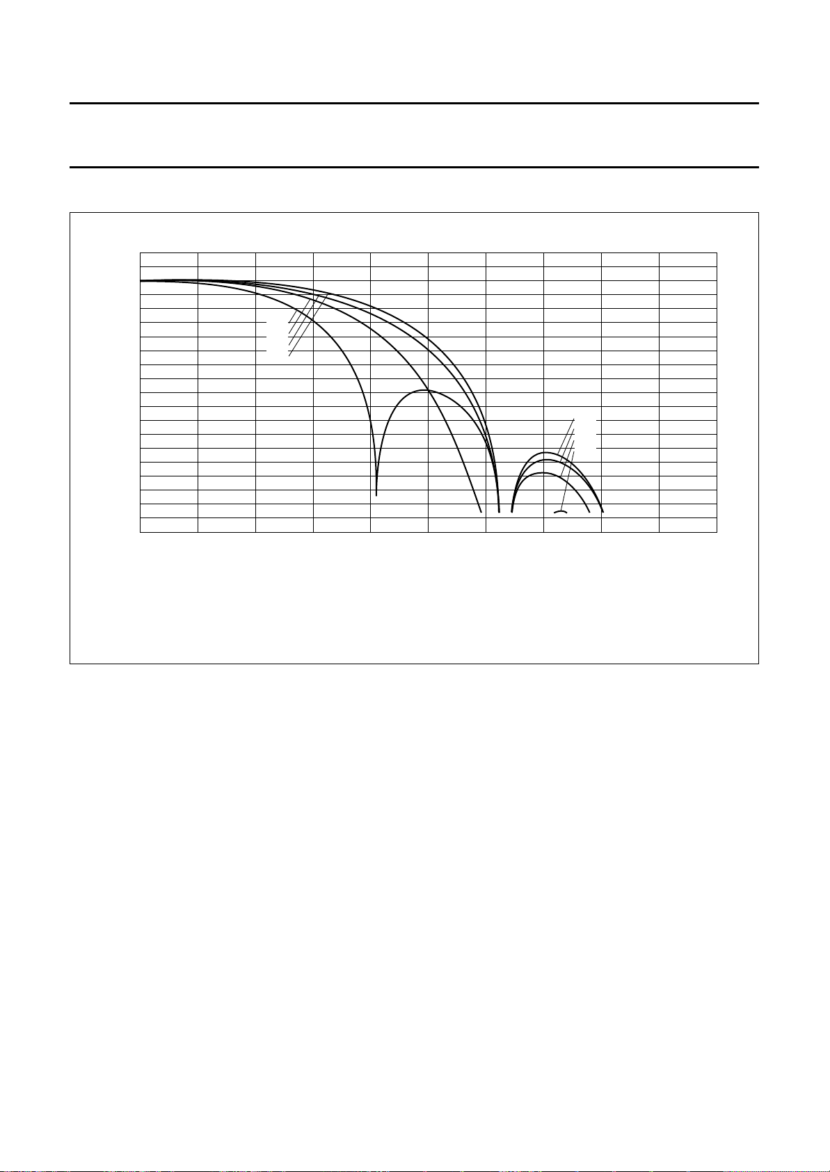
Philips Semiconductors Preliminary specification
Enhanced Video Input Processor (EVIP) SAA7111A
17.4 Chrominance filter curves
handbook, full pagewidth
6
V
(dB)
0
−6
(1)
−12
−18
−24
−30
−36
−42
−48
−54
0 0.54 1.08 1.62 2,16
Transfer characteristics of the chrominance low-pass dependent on CHBW[1 : 0] settings.
(1) CHBW [1 : 0] = 00; (2) CHBW [1 : 0] = 01; (3) CHBW [1 : 0] = 10; (4) CHBW [1 : 0] = 11.
(2)
(3)
(4)
Fig.51 Chrominance filter.
(4)
(1)
(3)
(2)
f
(MHz)
MGD147
2.7
2
C-BUS START SET-UP
18 I
• The given values force the following behaviour of the SAA7111A:
– the analog input AI11 expects a signal in CVBS format; analog anti-alias filter active
– automatic field detection
– YUV 4 :2:2 16-bit output format enabled
– outputs HS, HREF, VREF and VS active
– contrast, brightness and saturation control in accordance with CCIR standards
– chrominance processing with nominal bandwidth (800 kHz).
1996 Nov 07 62
Page 63
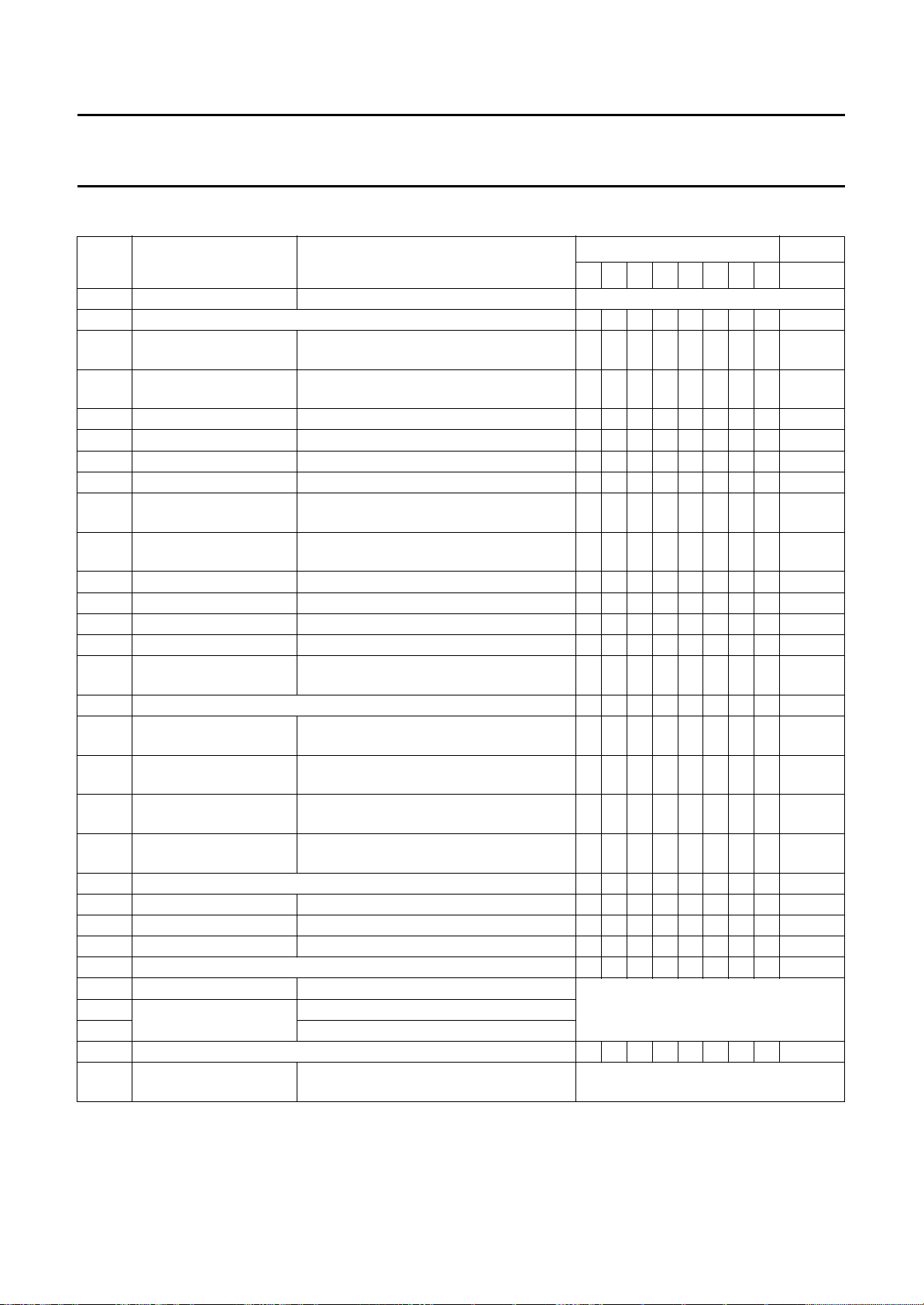
Philips Semiconductors Preliminary specification
Enhanced Video Input Processor (EVIP) SAA7111A
Table 40 I2C-bus start set-up values
SUB
(HEX)
00 chip version ID07 to ID00; see Table 8 read only
01 reserved 0 0000000 00
02 analog input control 1 FUSE1 and FUSE0, GUDL2 to GUDL0,
03 analog input control 2 X, HLNRS, VBSL, WPOFF, HOLDG,
04 analog input control 3 GAI17 to GAI10 0 0000000 00
05 analog input control 4 GAI27 to GAI20 0 0000000 00
06 horizontal sync start HSB7 to HSB0 1 1101011 EB
07 horizontal sync stop HSS7 to HSS0 1 1100000 E0
08 sync control AUFD, FSEL, EXFIL, X, VTRC, HPLL,
09 luminance control BYPS, PREF , BPSS1 and BPSS0, VBLB,
0A luminance brightness BRIG7 to BRIG0 1 0000000 80
0B luminance contrast CONT7 to CONT0 0 1000111 47
0C chrominance saturation SATN7 to SATN0 0 1000000 40
0D chroma hue control HUEC7 to HUEC0 0 0000000 00
0E chrominance control CDTO, CSTD2 to CSTD0, DCCF, FCTC,
0F reserved 0 0000000 00
10 format/delay control OFTS1 and OFTS0, YDEL2 to YDEL0
11 output control 1 GPSW, CM99, FECO, COMPO, OEYC,
12 output control 2 RTSE1 and RTSE0, TCLO, CBR,
13 output control 3 CCTR1 and CCTR0, BCHI1 and BCHI0,
14 reserved 0 0000000 00
15 VBI-data stream start VSTA7 to VSTA0 0 0000000 00
16 VBI-data stream stop VSTO7 to VSTO0 0 0000000 00
17 MSBs for VBI control X, X, X, X, X, X, VSTO8, VSTA8 0 0000000 00
18-19 reserved 0 0000000 00
1A text slicer status 0, 0, 0, 0, F2V AL, F2RDY, F1V AL, F1RDY read only register
1B decoded bytes of the
1C P2, BYTE2(6 to 0)
1D-1E reserved 0 0000000 00
1F status byte STTC, HLCK, FIDT, GLIMT, GLIMB,
FUNCTION NAME
MODE2 to MODE0
GAFIX, GAI28, GAI18
VNOI1 and VNOI0
UPTCV, APER1 and APER0
CHBW1 and CHBW0
HDEL1 and HDEL0, VRLN
OEHV, VIPB, COLO
RGB888 DIT, AOSL1 and AOSL0
BCLO1 and BCLO0, VCTR1 and VCTR0
P1, BYTE1(6 to 0)
text slicer
WIPA, SLTCA, CODE
(1)
VALUES (BIN) (HEX)
76543210START
11000000 C0
00100011 23
10001000 88
00000001 01
00000001 01
01000000 40
00011100 1C
00000001 01
00000000 00
read only register
Note
1. All X values must be set to LOW.
1996 Nov 07 63
Page 64
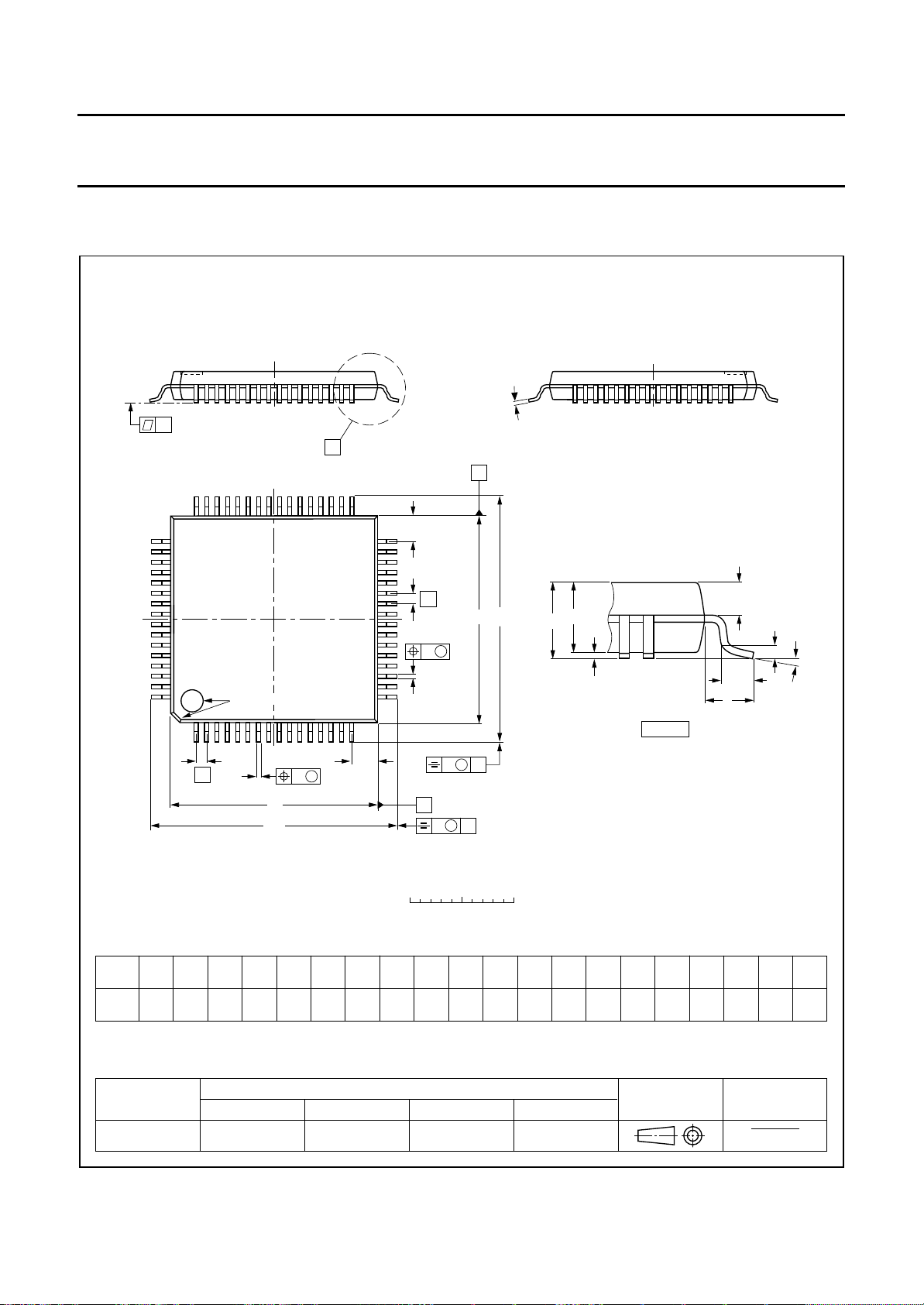
Philips Semiconductors Preliminary specification
Enhanced Video Input Processor (EVIP) SAA7111A
19 PACKAGE OUTLINES
LQFP64: plastic low profile quad flat package; 64 leads; body 10 x 10 x 1.4 mm
c
y
X
A
48 33
49
Z
32
E
SOT314-2
e
w M
b
p
64
DIMENSIONS (mm are the original dimensions)
mm
A
A1A2A3b
max.
0.20
1.60
0.05
UNIT
Note
1. Plastic or metal protrusions of 0.25 mm maximum per side are not included.
pin 1 index
1
e
1.45
0.25
1.35
w M
b
p
D
H
D
cE
p
0.27
0.18
0.17
0.12
17
16
Z
D
(1)
(1) (1)(1)
D
10.1
10.1
9.9
9.9
v M
B
v M
B
0 2.5 5 mm
scale
eH
H
12.15
0.5
11.85
D
E
A
12.15
11.85
Q
H
E
E
A
2
A
A
1
detail X
LLpQZywv θ
0.69
0.75
0.45
0.59
0.12 0.11.0 0.2
L
Z
1.45
1.05
(A )
3
θ
L
p
E
D
1.45
1.05
o
7
o
0
OUTLINE
VERSION
SOT314-2
1996 Nov 07 64
REFERENCES
IEC JEDEC EIAJ
EUROPEAN
PROJECTION
ISSUE DATE
94-01-07
95-12-19
Page 65
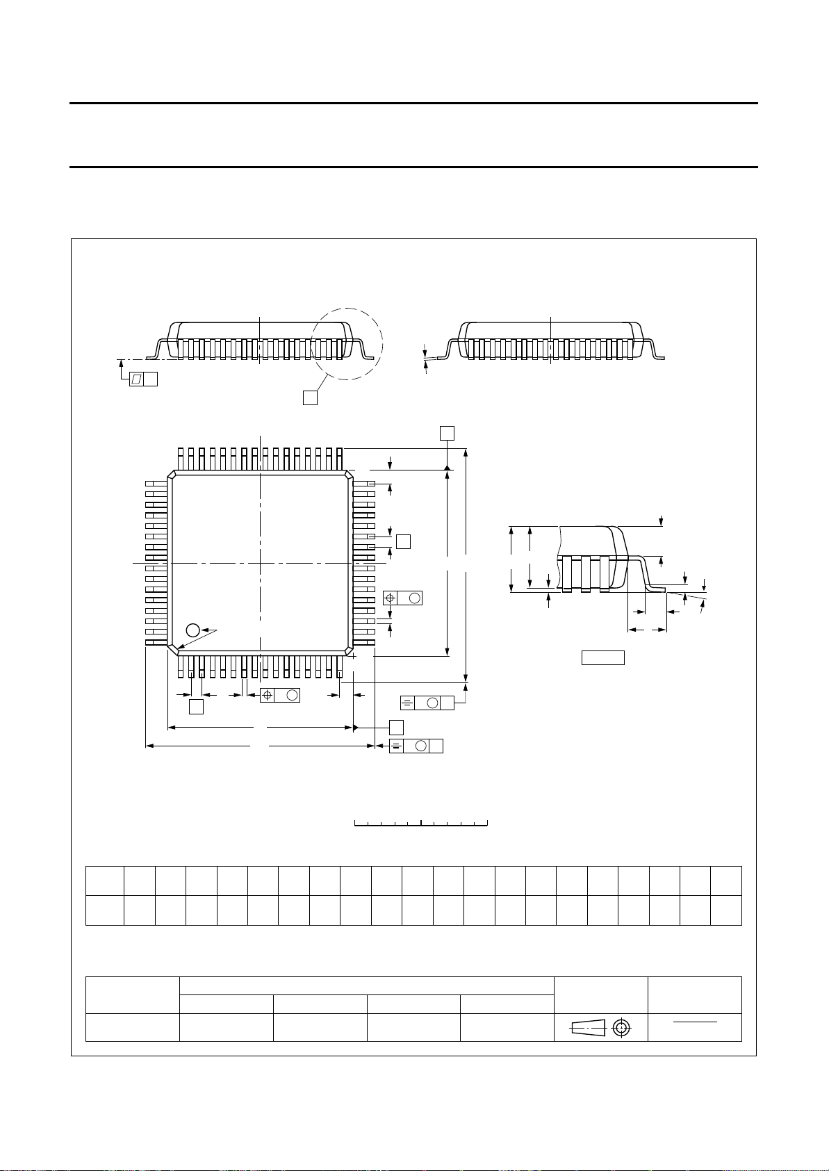
Philips Semiconductors Preliminary specification
Enhanced Video Input Processor (EVIP) SAA7111A
QFP64: plastic quad flat package; 64 leads (lead length 1.6 mm); body 14 x 14 x 2.7 mm
c
y
X
A
48 33
49
pin 1 index
64
1
32
Z
E
e
A
H
E
E
w M
b
p
17
16
2
A
A
1
detail X
SOT393-1
Q
(A )
3
θ
L
p
L
w M
b
e
DIMENSIONS (mm are the original dimensions)
UNIT A1A2A3b
Note
1. Plastic or metal protrusions of 0.25 mm maximum per side are not included.
A
max.
0.25
mm
3.00
OUTLINE
VERSION
SOT393-1 MS-022
0.10
2.75
2.55
p
D
H
D
cE
p
0.45
0.30
0.23
0.13
0.25
IEC JEDEC EIAJ
Z
D
B
v M
0 5 10 mm
(1)
(1) (1)(1)
D
14.1
13.9
REFERENCES
eH
14.1
13.9
0.8
17.45
16.95
1996 Nov 07 65
v M
scale
H
D
A
B
E
17.45
16.95
LLpQZywv θ
1.4
1.03
0.73
1.1
0.16 0.100.161.60
EUROPEAN
PROJECTION
Z
D
1.2
1.2
0.8
0.8
ISSUE DATE
94-06-22
96-05-21
E
o
7
o
0
Page 66
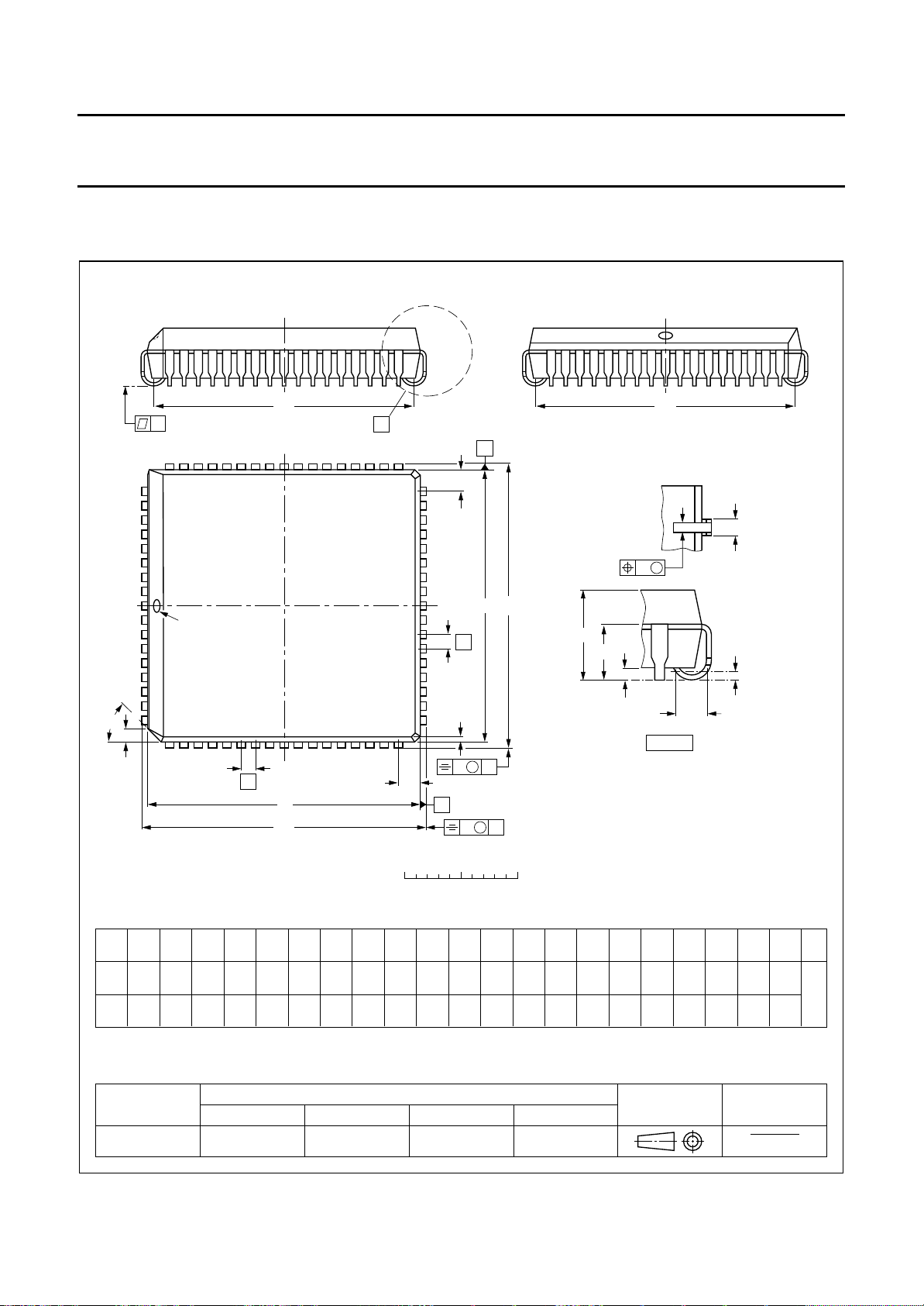
Philips Semiconductors Preliminary specification
Enhanced Video Input Processor (EVIP) SAA7111A
PLCC68: plastic leaded chip carrier; 68 leads
e
y
61
68
1
pin 1 index
D
X
SOT188-2
e
E
4460
43
A
Z
E
b
p
b
1
w M
H
E
E
e
A
A
1
A
4
(A )
3
k
9
β
1
27
k
10 26
e
Z
D
H
D
D
v M
A
B
v M
B
0 5 10 mm
scale
DIMENSIONS (millimetre dimensions are derived from the original inch dimensions)
UNIT A
mm
0.180
inches
0.165
A
1
min. max. max. max. max.
4.57
0.51
4.19
0.020
A
0.25
0.01
A
4
3
3.30
0.13
b
0.53
0.33
0.021
0.013
b
p
1
0.81
0.66
0.032
0.026
D
24.33
24.13
0.958
0.950
(1)
(1)
E
eH
e
D
1.27
0.05
23.62
22.61
0.930
0.890
24.33
24.13
0.958
0.950
e
23.62
22.61
0.930
0.890
H
D
E
25.27
25.27
25.02
25.02
0.995
0.995
0.985
0.985
Note
1. Plastic or metal protrusions of 0.01 inches maximum per side are not included.
OUTLINE
VERSION
SOT188-2
IEC JEDEC EIAJ
112E10 MO-047AC
REFERENCES
k
1
k
E
1.22
1.07
0.048
0.042
0.51
0.020
L
1.44
1.02
0.057
0.040
detail X
p
0.007 0.0040.007
EUROPEAN
PROJECTION
L
p
(1) (1)
Z
Z
E
D
ywv β
0.18 0.100.18
2.16
0.085
2.16
0.085
o
45
ISSUE DATE
92-11-17
95-03-11
1996 Nov 07 66
Page 67

Philips Semiconductors Preliminary specification
Enhanced Video Input Processor (EVIP) SAA7111A
20 SOLDERING
20.1 Introduction
There is no soldering method that is ideal for all IC
packages. Wave soldering is often preferred when
through-hole and surface mounted components are mixed
on one printed-circuit board. However, wave soldering is
not always suitable for surface mounted ICs, or for
printed-circuits with high population densities. In these
situations reflow soldering is often used.
This text gives a very brief insight to a complex technology.
A more in-depth account of soldering ICs can be found in
our
“IC Package Databook”
20.2 Reflow soldering
Reflow soldering techniques are suitable for all PLCC and
QFP packages.
The choice of heating method may be influenced by larger
PLCC or QFP packages (44 leads, or more). If infrared or
vapour phase heating is used and the large packages are
not absolutely dry (less than 0.1% moisture content by
weight), vaporization of the small amount of moisture in
them can cause cracking of the plastic body. For more
information, refer to the Drypack chapter in our
Reference Handbook”
Reflow soldering requires solder paste (a suspension of
fine solder particles, flux and binding agent) to be applied
to the printed-circuit board by screen printing, stencilling or
pressure-syringe dispensing before package placement.
Several techniques exist for reflowing; for example,
thermal conduction by heated belt. Dwell times vary
between 50 and 300 seconds depending on heating
method. Typical reflow temperatures range from
215 to 250 °C.
(order code 9398 652 90011).
“Quality
(order code 9397 750 00192).
• The package footprint must incorporate solder thieves at
the downstream corners.
20.3.2 QFP
Wave soldering is not recommended for QFP packages.
This is because of the likelihood of solder bridging due to
closely-spaced leads and the possibility of incomplete
solder penetration in multi-lead devices.
If wave soldering cannot be avoided, the following
conditions must be observed:
• A double-wave (a turbulent wave with high upward
pressure followed by a smooth laminar wave)
soldering technique should be used.
• The footprint must be at an angle of 45° to the board
direction and must incorporate solder thieves
downstream and at the side corners.
Even with these conditions, do not consider wave
soldering the following packages: QFP52 (SOT379-1),
QFP100 (SOT317-1), QFP100 (SOT317-2),
QFP100 (SOT382-1) or QFP160 (SOT322-1).
20.3.3 M
During placement and before soldering, the package must
be fixed with a droplet of adhesive. The adhesive can be
applied by screen printing, pin transfer or syringe
dispensing. The package can be soldered after the
adhesive is cured.
Maximum permissible solder temperature is 260 °C, and
maximum duration of package immersion in solder is
10 seconds, if cooled to less than 150 °C within
6 seconds. Typical dwell time is 4 seconds at 250 °C.
A mildly-activated flux will eliminate the need for removal
of corrosive residues in most applications.
ETHOD (PLCC AND QFP)
Preheating is necessary to dry the paste and evaporate
the binding agent. Preheating duration: 45 minutes at
45 °C.
20.3 Wave soldering
20.3.1 PLCC
Wave soldering techniques can be used for all PLCC
packages if the following conditions are observed:
• A double-wave (a turbulent wave with high upward
pressure followed by a smooth laminar wave) soldering
technique should be used.
• The longitudinal axis of the package footprint must be
parallel to the solder flow.
1996 Nov 07 67
20.4 Repairing soldered joints
Fix the component by first soldering two diagonallyopposite end leads. Use only a low voltage soldering iron
(less than 24 V) applied to the flat part of the lead. Contact
time must be limited to 10 seconds at up to 300 °C. When
using a dedicated tool, all other leads can be soldered in
one operation within 2 to 5 seconds between
270 and 320 °C.
Page 68
Philips Semiconductors Preliminary specification
Enhanced Video Input Processor (EVIP) SAA7111A
21 DEFINITIONS
Data sheet status
Objective specification This data sheet contains target or goal specifications for product development.
Preliminary specification This data sheet contains preliminary data; supplementary data may be published later.
Product specification This data sheet contains final product specifications.
Limiting values
Limiting values given are in accordance with the Absolute Maximum Rating System (IEC 134). Stress above one or
more of the limiting values may cause permanent damage to the device. These are stress ratings only and operation
of the device at these or at any other conditions above those given in the Characteristics sections of the specification
is not implied. Exposure to limiting values for extended periods may affect device reliability.
Application information
Where application information is given, it is advisory and does not form part of the specification.
22 LIFE SUPPORT APPLICATIONS
These products are not designed for use in life support appliances, devices, or systems where malfunction of these
products can reasonably be expected to result in personal injury. Philips customers using or selling these products for
use in such applications do so at their own risk and agree to fully indemnify Philips for any damages resulting from such
improper use or sale.
23 PURCHASE OF PHILIPS I
Purchase of Philips I
components in the I2C system provided the system conforms to the I2C specification defined by
Philips. This specification can be ordered using the code 9398 393 40011.
2
C COMPONENTS
2
C components conveys a license under the Philips’ I2C patent to use the
1996 Nov 07 68
 Loading...