

Page 1

INTEGRATED CIRCUITS
DATA SH EET
SAA6750H
Encoder for MPEG2 image
recording (EMPIRE)
Preliminary specification
File under Integrated Circuits, IC02
1998 Sep 07
Page 2

Philips Semiconductors Preliminary specification
Encoder for MPEG2 image recording
(EMPIRE)
CONTENTS
1 FEATURES
2 GENERAL DESCRIPTION
2.1 General
2.2 Function
2.3 Application fields
2.3.1 General
2.3.2 Video editing (PC applications)
2.3.3 Camera signal transmission
2.3.4 DVD authoring
2.3.5 Video recording for surveillance
2.3.6 Digital VCR
3 QUICK REFERENCE DATA
4 ORDERING INFORMATION
5 BLOCK DIAGRAM
6 PINNING
7 FUNCTIONAL DESCRIPTION
7.1 Global architecture description
7.1.1 General
7.1.2 Architecture structure
7.2 Start-up and operation modes
7.2.1 Start-up requirements
7.2.2 Reset processing
7.2.3 Description of operation modes
7.2.4 Pin behaviour
7.3 Video front-end and formatter
7.3.1 General
7.3.2 Data input format
7.3.3 Functional description
7.4 MacroBlock Processor (MBP)
7.4.1 General
7.4.2 Functional description
7.5 Bit stream assembly
7.5.1 General
7.5.2 Pre-packer and packer
7.5.3 Stuffing unit and output buffer
7.6 Data output port
7.6.1 General
7.6.2 Data output format
7.6.3 Functional description
SAA6750H
7.7 Application Specific Instruction-set Processor
(ASIP)
7.7.1 General
7.7.2 ASIP software
7.7.3 GPIO port
7.8 Global controller
7.8.1 General
7.8.2 Functional description
7.9 I2C-bus interface and controller
7.9.1 General
7.9.2 Special considerations
7.9.3 I2C-bus data transfer modes
7.9.4 I2C-bus memories and registers
7.9.5 I2C-bus initialization
7.10 DRAM interface
7.10.1 General
7.10.2 Application hints
7.10.3 Functional description
7.11 FIFO memories
7.12 Clock distribution
7.13 Input/output levels
7.14 Boundary scan test
7.14.1 General
7.14.2 Initialization of boundary scan circuit
7.14.3 Device identification codes
8 LIMITING VALUES
9 THERMAL CHARACTERISTICS
10 CHARACTERISTICS
11 APPLICATION INFORMATION
12 PACKAGE OUTLINE
13 SOLDERING
13.1 Introduction
13.2 Reflow soldering
13.3 Wave soldering
13.4 Repairing soldered joints
14 DEFINITIONS
15 LIFE SUPPORT APPLICATIONS
16 PURCHASE OF PHILIPS I2C COMPONENTS
1998 Sep 07 2
Page 3

Philips Semiconductors Preliminary specification
Encoder for MPEG2 image recording
(EMPIRE)
1 FEATURES
• Digital YUV input according to
“ITU-T 656”
• NTSC and PAL (720 pixel × 480 lines at 60 Hz and
720 pixel × 576 lines at 50 Hz)
• Integrated colour conversion 4 :2:2to4:2:0
• Integrated format conversion to SIF format (optional)
• Real time MPEG2 Simple Profile at Main Level
(SP@ML) encoding
• IP frame or I frame only encoding supported
• Programmable Group Of Pictures (GOP) size
• Integrated motion estimation, half pixel accuracy,
search range 128 × 128 pixels
• Motion compensated noise reduction
• Elementary stream data output compliant to MPEG2
standard (
• Constant Bit-Rate (CBR) and Variable Bit-Rate (VBR)
supported
• Bitstream output compatible to 16-bit parallel interface
with Motorola (68xxx like) or Intel (xxx86 like) protocol
style
• Adaptable to dedicated applications by embedded
software
• Standard software package available (refer to software
specification)
• No external host processor required
• High speed real time port for processor co-processor
applications
• Only 4 × 4 Mbit external DRAM required
• I2C-bus controlled
• Single external video clock 27 MHz
• Power supply 3.3 V
• Digital inputs 5 V tolerant
• Boundary Scan Test (BST) supported.
“ISO 13818-2”
)
“ITU-T 601”
and to
SAA6750H
2 GENERAL DESCRIPTION
2.1 General
The SAA6750H is a new approach towards a stand-alone
MPEG2 video encoder IC. It combines high quality
SP at ML compliant real time encoding with
cost-effectiveness, allowing for the first time the use of an
MPEG2 encoder IC in applications and markets with a high
cost pressure. This has been achieved by means of a
number of innovations in architecture and algorithms
developed by the Philips Research Laboratories. E.g.:
• The unique motion estimation algorithm supports highly
efficient encoding by using only I frame and IP frame
mode. B frames need not be used. This leads to a
significantly smaller internal circuitry and also reduces
DRAM memory requirements from at least 4 to 2 Mbyte.
In addition, the absence of B frames simplifies editing of
the compressed data stream.
• The patented, motion-compensated temporal noise
filtering which was developed by Philips for professional
equipment reduces noise in the input video before
compression is performed. This technique gives visible
improvements in picture quality, especially in the field of
home recordings with noisy signal sources where this
has proved to be of significant benefit.
Internally the SAA6750H uses a hardware solution for data
compression and a specially developed high performance
processor for control purposes. This programmable
embedded Digital Signal Processor (DSP) approach
allows Philips to tailor various customized sets of functions
for this IC. Contact Philips for information on available
software packages.
1998 Sep 07 3
Page 4

Philips Semiconductors Preliminary specification
Encoder for MPEG2 image recording
(EMPIRE)
2.2 Function
The SAA6750H is a stand-alone single chip video encoder
performing real time MPEG2 compression of digital video
data.
The video data input of the SAA6750H accepts a digital
YUV video data stream in ITU-T 601-format. PAL standard
at 50 Hz and 720 pixel by 576 lines, as well as NTSC at
60 Hz and 720 pixel by 480 lines, are covered. The video
synchronization may either follow ITU-T 656
recommendation or can also be supplied by external
signals. The external reference clock VCLK = 27 MHz has
to be synchronized to the video data.
Philips Semiconductor’s SAA7111 product family provides
a suitable video data stream and reference clock.
Other sources are also supported by the flexible I
controlled data input interface of the SAA6750H.
See Section 7.3 for detailed information.
An internal 4:2:2to4:2:0 colour format conversion is
performed. Optionally, a ITU-T 601 to SIF format
conversion may be activated by I2C-bus control settings.
The real time data encoding part of the SAA6750H
combines high-compression rates with high quality picture
performance. This is achieved by the integration of Philips
unique motion estimation algorithm, providing a search
range of 128 by 128 pixels, and a patented
motion-compensated noise filtering. The compression
algorithm uses I or IP mode encoding. Normally it selects
automatically the suitable mode but may also be forced
only to I mode operation by I2C-bus control settings.
In contrast to the encoding part which is designed in
dedicated hardware, control functions and data stream
handling tasks like e.g. header generation and bit-rate
control are carried out by a dedicated control processor,
the so-called Application Specific Instruction-set
Processor (ASIP). The ASIP’s microcode is contained in
an internal RAM and is loaded via I2C-bus before start of
operation. This architecture allows Philips to customize the
SAA6750H to specific applications by generating different
versions of the embedded microcode. Philips will provide
software packages for several applications.
The ASIP is able to communicate with the outside world by
I2C-bus and by a high speed parallel port, the GPIO port.
The SAA6750H generates an MPEG2 Elementary Stream
(ES) in accordance with the MPEG2 standard
(
“ISO 13818-2”
Variable Bit-Rate (VBR) output data can be generated.
The 16-bit data output interface supports Motorola
(68xxx like) and Intel (xxx86 like) protocol style.
). Either Constant Bit-Rate (CBR) or
2
C-bus
SAA6750H
Data processing and control functions are managed by
loosely coupled processes. FIFO memories are used to
connect these processes. In addition to these internal
storages the SAA6750H needs 4 × 4 Mbit of external
DRAM memory (t
in Fig.1.
Selectable I2C-bus addresses and a special reset mode
affecting the output pin behaviour allow the use of two
SAA6750H devices in one application.
2.3 Application fields
2.3.1 G
The SAA6750H can be applied within the following
application domains:
• Video editing (PC applications)
• Camera signal transmission
• Digital Versatile Disc (DVD) authoring
• Video recording for surveillance
• Digital VCR.
All those systems have to compress video data in order to
manage the storage or transmission of digitized video
data. The SAA6750H can be handled for most of the
applications as a stand-alone device. That means at
start-up a microcode and a couple of I2C-bus settings are
loaded and the SAA6750H is started. If needed, settings
like GOP size or bit-rate are changed on-the-fly via
I2C-bus.
Two basic modes of encoding will be supported by
standard microcode packages: Encoding at VBR or CBR.
The GPIO port allows high speed data exchange between
the embedded DSP and an external processor. Therefore
applications like DVD-authoring are supported.
2.3.2 V
For video editing the SAA6750H can be interfaced
gluelessly to a video input processor with ITU-T 565
compliant digital video output. In order to link the SA6750H
to the PC, the use of the PCI bridge SAA7146 is
recommend. By this bridge the MPEG2 video ES can be
transmitted via the PCI-bus on a Hard Disc (HD).
Furthermore all I2C-bus settings can be send from the PC
via the bridge to the I2C components on the encoder
board. The SAA7146 supports Pulse Code Modulation
(PCM) audio capturing. Multiplexing with an audio stream
or audio encoding can be done by the PC’s CPU. A block
diagram is shown in Fig.23.
ENERAL
IDEO EDITING (PC APPLICATIONS)
= 60 ns). A block diagram is shown
RAC
1998 Sep 07 4
Page 5

Philips Semiconductors Preliminary specification
Encoder for MPEG2 image recording
(EMPIRE)
2.3.3 CAMERA SIGNAL TRANSMISSION
In this application the SAA6750H will be located within a
camera to compress the received digital video data for
transmission. Typically VBR mode will be used.
2.3.4 DVD
For DVD authoring the video data has to be encoded in
two steps. During the first step the complexity of the video
sequence is measured and the results are stored
externally. During the second pass the measured
complexity is used as an input for the bit-rate control.
This application can be realized by a processor
co-processor approach. The SAA6750H, which is working
as a co-processor, and a host processor are
communicating via the GPIO port. A specific microcode
package supports this mode.
2.3.5 V
For surveillance systems VCRs with a huge amount of
storage capacity are required. A high picture resolution is
AUTHORING
IDEO RECORDING FOR SURVEILLANCE
SAA6750H
very important when there is action in the captured picture.
The SAA6750H can control its encoded bit-rate by motion
detection by its integrated motion estimation algorithm.
Doing so the bit-rate can vary from 0.5 to 10 Mbit/s.
VCRs with a storage space of 6 month are possible.
2.3.6 D
In stand-alone VCRs the SAA6750H works together with
an audio encoder and a multiplexer. The SAA6750H is
clocked by the video clock of the video input processor
(SAA7111 or derivatives). A master clock is derived from
the frame pulse. The video clock and master clock domain
are de-coupled by a FIFO. The audio clock can be derived
from the master clock. The video Packetized Elementary
Stream (PES) packatizer has to take care of the fullness of
SAA6750H’s output buffer.
IGITAL VCR
3 QUICK REFERENCE DATA
SYMBOL PARAMETER MIN. TYP. MAX. UNIT
V
DD
I
DD(tot)
P
tot
f
VCLK
f
SCL
digital supply voltage 3.0 3.3 3.6 V
total digital supply current − tbf 0.56 mA
total power dissipation − tbf 2.0 W
video clock frequency 25.6 27.0 28.6 MHz
I2C-bus input clock frequency 100 − 400 kHz
B output bit-rate 1.5 − 40 Mbit/s
V
IH
V
IL
V
OH
V
OL
T
amb
HIGH-level digital input voltage 2.0 − 5.5 V
LOW-level digital input voltage −0.5 − +0.8 V
HIGH-level digital output voltage 2.4 − V
DD
V
LOW-level digital output voltage −−0.4 V
operating ambient temperature 0 − 70 °C
4 ORDERING INFORMATION
TYPE
NUMBER
NAME DESCRIPTION VERSION
SAA6750H SQFP208 plastic shrink quad flat package; 208 leads (lead length 1.3 mm);
PACKAGE
SOT316-1
body 28 × 28 × 3.4 mm
1998 Sep 07 5
Page 6
This text is here in white to force landscape pages to be rotated correctly when browsing through the pdf in the Acrobat reader.This text is here in
_white to force landscape pages to be rotated correctly when browsing through the pdf in the Acrobat reader.This text is here inThis text is here in
white to force landscape pages to be rotated correctly when browsing through the pdf in the Acrobat reader. white to force landscape pages to be ...
1998 Sep 07 6
YUV7 to
YUV0
FID
HSYNC
VSYNC
MAD
SDA
SCL
VCLK
(27 MHz)
RESETN
87 to 84,
74 to 71
89
90
91
97
98
99
93
96
V
DD
+3.3 V
6, 16, 28, 38,
18
48, 58, 66, 88,
94, 100, 110,
120, 142, 152,
166, 176, 194,
204
8
start
I2C-BUS
TRANSCEIVER
CLOCK
GENERATION
18
V
DDCO
+3.3 V
22, 24, 26, 76,
16
78, 80, 82,
126, 128, 130,
132, 134, 162,
178, 180, 182
27 MHz
1, 11, 21, 33,
43, 53, 63, 70,
92, 95, 105, 115,
137, 147, 157,
171, 189, 199
CASN
65 67 68 69
PROCESSING
SAA6750H
23, 25, 27, 75,
77, 79, 81, 83,
127, 129, 131,
133, 177, 179,
16
181, 183
RASN
WEN OEN
DRAM INTERFACE
LINE
BASED
GLOBAL CONTROL ASIP
ADR8 to ADR0
64,
62 to 59,
57 to 54
9
MACROBLOCK
BASED
PROCESSING
TEST CONTROL BLOCK
FOR
BOUNDARY SCAN TEST
AND
SCAN TEST
BITSTREAM
PROCESSING
DATA63 to DATA0
52 to 49, 47 to 44,
42 to 39, 37 to 34,
32 to 29, 20 to 17,
15 to 12, 10 to 7,
5 to 2, 208 to 205,
203 to 200, 198 to 195,
193 to 190, 188 to 185,
64
175 to 172, 170 to 167
BASED
DATA
OUTPUT
PORT
GPIO
PORT
184164 165160159 163161
101
121
122
124
125
138 to 141,
143 to 146,
148 to 151,
153 to 156
16
123
135
136
102
103
119 to 116,
114 to 111,
109 to 106
12
104
158
MEM_ST
LRQN
URQN
I_MN
CSN
AD15
to AD0
DTACK_RDY
AS_ALE
DS_RDN
FAD_RWN
FAD_EN
GPIO11
to GPIO0
FAD_RDYN
TDO
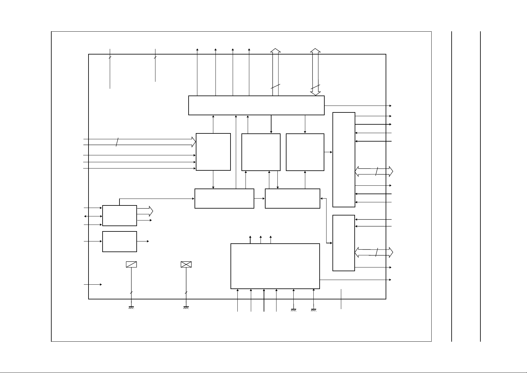
5 BLOCK DIAGRAM
Encoder for MPEG2 image recording
(EMPIRE)
SAA6750H
Philips Semiconductors Preliminary specification
V
SS
V
SSCO
CS_TEST n.c.
TESTTMS TDITRST TCK
Fig.1 Block diagram.
Page 7

Philips Semiconductors Preliminary specification
Encoder for MPEG2 image recording
(EMPIRE)
6 PINNING
I
max
SYMBOL PIN INPUT/OUTPUT
V
SS
1 ground − ground for pad ring
DATA28 2 input/output 3 DRAM data interface bit 28
DATA29 3 input/output 3 DRAM data interface bit 29
DATA30 4 input/output 3 DRAM data interface bit 30
DATA31 5 input/output 3 DRAM data interface bit 31
V
DD
6 supply − supply voltage for pad ring
DATA32 7 input/output 3 DRAM data interface bit 32
DATA33 8 input/output 3 DRAM data interface bit 33
DATA34 9 input/output 3 DRAM data interface bit 34
DATA35 10 input/output 3 DRAM data interface bit 35
V
SS
11 ground − ground for pad ring
DATA36 12 input/output 3 DRAM data interface bit 36
DATA37 13 input/output 3 DRAM data interface bit 37
DATA38 14 input/output 3 DRAM data interface bit 38
DATA39 15 input/output 3 DRAM data interface bit 39
V
DD
16 supply − supply voltage for pad ring
DATA40 17 input/output 3 DRAM data interface bit 40
DATA41 18 input/output 3 DRAM data interface bit 41
DATA42 19 input/output 3 DRAM data interface bit 42
DATA43 20 input/output 3 DRAM data interface bit 43
V
SS
V
DDCO
V
SSCO
V
DDCO
V
SSCO
V
DDCO
V
SSCO
V
DD
21 ground − ground for pad ring
22 supply − supply voltage for core logic
23 ground − ground for core logic
24 supply − supply voltage for core logic
25 ground − ground for core logic
26 supply − supply voltage for core logic
27 ground − ground for core logic
28 supply − supply voltage for pad ring
DATA44 29 input/output 3 DRAM data interface bit 44
DATA45 30 input/output 3 DRAM data interface bit 45
DATA46 31 input/output 3 DRAM data interface bit 46
DATA47 32 input/output 3 DRAM data interface bit 47
V
SS
33 ground − ground for pad ring
DATA48 34 input/output 3 DRAM data interface bit 48
DATA49 35 input/output 3 DRAM data interface bit 49
DATA50 36 input/output 3 DRAM data interface bit 50
DATA51 37 input/output 3 DRAM data interface bit 51
V
DD
38 supply − supply voltage for pad ring
DATA52 39 input/output 3 DRAM data interface bit 52
(1)
(mA)
SAA6750H
DESCRIPTION
1998 Sep 07 7
Page 8

Philips Semiconductors Preliminary specification
Encoder for MPEG2 image recording
(EMPIRE)
I
max
SYMBOL PIN INPUT/OUTPUT
DATA53 40 input/output 3 DRAM data interface bit 53
DATA54 41 input/output 3 DRAM data interface bit 54
DATA55 42 input/output 3 DRAM data interface bit 55
V
SS
43 ground − ground for pad ring
DATA56 44 input/output 3 DRAM data interface bit 56
DATA57 45 input/output 3 DRAM data interface bit 57
DATA58 46 input/output 3 DRAM data interface bit 58
DATA59 47 input/output 3 DRAM data interface bit 59
V
DD
48 supply − supply voltage for pad ring
DATA60 49 input/output 3 DRAM data interface bit 60
DATA61 50 input/output 3 DRAM data interface bit 61
DATA62 51 input/output 3 DRAM data interface bit 62
DATA63 52 input/output 3 DRAM data interface bit 63 (MSB)
V
SS
53 ground − ground for pad ring
ADR0 54 output/3-state 3 DRAM address interface bit 0 (LSB)
ADR1 55 output/3-state 3 DRAM address interface bit 1
ADR2 56 output/3-state 3 DRAM address interface bit 2
ADR3 57 output/3-state 3 DRAM address interface bit 3
V
DD
58 supply − supply voltage for pad ring
ADR4 59 output/3-state 3 DRAM address interface bit 4
ADR5 60 output/3-state 3 DRAM address interface bit 5
ADR6 61 output/3-state 3 DRAM address interface bit 6
ADR7 62 output/3-state 3 DRAM address interface bit 7
V
SS
63 ground − ground for pad ring
ADR8 64 output/3-state 3 DRAM address interface bit 8 (MSB)
CASN 65 output/3-state 6 DRAM column address strobe (active LOW)
V
DD
66 supply − supply voltage for pad ring
RASN 67 output/3-state 3 DRAM row address strobe (active LOW)
WEN 68 output/3-state 3 DRAM write enable (active LOW)
OEN 69 output/3-state 3 DRAM chip select (active LOW)
V
SS
70 ground − ground for pad ring
YUV0 71 input − video input signal bit 0 (LSB)
YUV1 72 input − video input signal bit 1
YUV2 73 input − video input signal bit 2
YUV3 74 input − video input signal bit 3
V
SSCO
V
DDCO
V
SSCO
V
DDCO
V
SSCO
75 ground − ground for core logic
76 supply − supply voltage for core logic
77 ground − ground for core logic
78 supply − supply voltage for core logic
79 ground − ground for core logic
(1)
(mA)
DESCRIPTION
SAA6750H
1998 Sep 07 8
Page 9

Philips Semiconductors Preliminary specification
Encoder for MPEG2 image recording
(EMPIRE)
I
max
SYMBOL PIN INPUT/OUTPUT
V
DDCO
V
SSCO
V
DDCO
V
SSCO
80 supply − supply voltage for core logic
81 ground − ground for core logic
82 supply − supply voltage for core logic
83 ground − ground for core logic
YUV4 84 input − video input signal bit 4
YUV5 85 input − video input signal bit 5
YUV6 86 input − video input signal bit 6
YUV7 87 input − video input signal bit 7 (MSB)
V
DD
88 supply − supply voltage for pad ring
FID 89 input − odd/even field identification
HSYNC 90 input − horizontal reference signal
VSYNC 91 input − vertical reference signal
V
SS
92 ground − ground for pad ring
VCLK 93 input − video clock input (27 MHz)
V
DD
V
SS
94 supply − supply voltage for pad ring
95 ground − ground for pad ring
RESETN 96 input − hard reset input (active LOW)
MAD 97 input − module address (I2C-bus)
SDA 98 input/open drain output 6 serial data input/output (I
SCL 99 input/open drain output − serial clock input (I
V
DD
100 supply − supply voltage for pad ring
MEM_ST 101 output/3-state 3 do not use in the application (reserved)
FAD_RWN 102 input − ASIP port data read/
FAD_EN 103 input − ASIP port data enable
FAD_RDYN 104 open drain output 3 ASIP port data ready (active LOW)
V
SS
105 ground − ground for pad ring
GPIO0 106 input/output 3 ASIP port data bit 0 (LSB)
GPIO1 107 input/output 3 ASIP port data bit 1
GPIO2 108 input/output 3 ASIP port data bit 2
GPIO3 109 input/output 3 ASIP port data bit 3
V
DD
110 supply − supply voltage for pad ring
GPIO4 111 input/output 3 ASIP port data bit 4
GPIO5 112 input/output 3 ASIP port data bit 5
GPIO6 113 input/output 3 ASIP port data bit 6
GPIO7 114 input/output 3 ASIP port data bit 7
V
SS
115 ground − ground for pad ring
GPIO8 116 input/output 3 ASIP port data bit 8
GPIO9 117 input/output 3 ASIP port data bit 9
GPIO10 118 input/output 3 ASIP port data bit 10
GPIO11 119 input/output 3 ASIP port data bit 11 (MSB)
(1)
(mA)
DESCRIPTION
2
C-bus)
2
C-bus)
write
SAA6750H
1998 Sep 07 9
Page 10

Philips Semiconductors Preliminary specification
Encoder for MPEG2 image recording
SAA6750H
(EMPIRE)
I
max
SYMBOL PIN INPUT/OUTPUT
V
DD
120 supply − supply voltage for pad ring
(1)
(mA)
LRQN 121 open drain output 3 output port lower watermark interrupt request (active LOW)
URQN 122 open drain/3-state 3 output port upper watermark interrupt request (active LOW)
DTACK_RDY 123 open drain output 3 output port data transfer acknowledge/ready/request
I_MN 124 input − output port Intel/Motorola bus style selection input
(active LOW); with internal pull-up resistor
CSN 125 input − output port chip select for external address mode (active LOW);
with internal pull-up resistor
V
DDCO
V
SSCO
V
DDCO
V
SSCO
V
DDCO
V
SSCO
V
DDCO
V
SSCO
V
DDCO
126 supply − supply voltage for core logic
127 ground − ground for core logic
128 supply − supply voltage for core logic
129 ground − ground for core logic
130 supply − supply voltage for core logic
131 ground − ground for core logic
132 supply − supply voltage for core logic
133 ground − ground for core logic
134 supply − supply voltage for core logic
AS_ALE 135 input − output port address strobe/address latch enable
DS_RDN 136 input − output port data strobe/read
V
SS
137 ground − ground for pad ring
AD15 138 input/output 3 output port multiplexed address/data line bit 15 (MSB)
AD14 139 input/output 3 output port multiplexed address/data line bit 14
AD13 140 input/output 3 output port multiplexed address/data line bit 13
AD12 141 input/output 3 output port multiplexed address/data line bit 12
V
DD
142 supply − supply voltage for pad ring
AD11 143 input/output 3 output port multiplexed address/data line bit 11
AD10 144 input/output 3 output port multiplexed address/data line bit 10
AD9 145 input/output 3 output port multiplexed address/data line bit 9
AD8 146 input/output 3 output port multiplexed address/data line bit 8
V
SS
147 ground − ground for pad ring
AD7 148 input/output 3 output port multiplexed address/data line bit 7/data bus bit 7
(MSB)
AD6 149 input/output 3 output port multiplexed address/data line bit 6/data bus bit 6
AD5 150 input/output 3 output port multiplexed address/data line bit 5/data bus bit 5
AD4 151 input/output 3 output port multiplexed address/data line bit 4/data bus bit 4
V
DD
152 supply − supply voltage for pad ring
AD3 153 input/output 3 output port multiplexed address/data line bit 3/data bus bit 3
AD2 154 input/output 3 output port multiplexed address/data line bit 2/data bus bit 2
AD1 155 input/output 3 output port multiplexed address/data line bit 1/data bus bit 1
AD0 156 input/output 3 output port multiplexed address/data line bit 0 (LSB)/data bus
bit 0 (LSB)
DESCRIPTION
1998 Sep 07 10
Page 11

Philips Semiconductors Preliminary specification
Encoder for MPEG2 image recording
SAA6750H
(EMPIRE)
I
max
SYMBOL PIN INPUT/OUTPUT
V
SS
157 ground − ground for pad ring
TDO 158 output 3 boundary scan test data output; pin not active during normal
TRST 159 input − boundary scan test reset; pin must be set to LOW for normal
TCK 160 input − boundary scan test clock; pin must be set to LOW during normal
TMS 161 input − boundary scan test mode select; pin must float or set to HIGH
V
DDCO
162 supply − supply voltage for core logic
TDI 163 input − boundary scan test data input; pin must float or set to HIGH
CS_TEST 164 input − test mode for the internal RAMs; pin must be set to LOW during
TEST 165 input − test mode; pin must be set to LOW during normal operation
V
DD
166 supply − supply voltage for pad ring
DATA0 167 input/output 3 DRAM data interface bit 0 (LSB)
DATA1 168 input/output 3 DRAM data interface bit 1
DATA2 169 input/output 3 DRAM data interface bit 2
DATA3 170 input/output 3 DRAM data interface bit 3
V
SS
171 ground − ground for pad ring
DATA4 172 input/output 3 DRAM data interface bit 4
DATA5 173 input/output 3 DRAM data interface bit 5
DATA6 174 input/output 3 DRAM data interface bit 6
DATA7 175 input/output 3 DRAM data interface bit 7
V
DD
V
SSCO
V
DDCO
V
SSCO
V
DDCO
V
SSCO
V
DDCO
V
SSCO
176 supply − supply voltage for pad ring
177 ground − ground for core logic
178 supply − supply voltage for core logic
179 ground − ground for core logic
180 supply − supply voltage for core logic
181 ground − ground for core logic
182 supply − supply voltage for core logic
183 ground − ground for core logic
n.c. 184 −−reserved pin; do not connect
DATA8 185 input/output 3 DRAM data interface bit 8
DATA9 186 input/output 3 DRAM data interface bit 9
DATA10 187 input/output 3 DRAM data interface bit 10
DATA11 188 input/output 3 DRAM data interface bit 11
V
SS
189 ground − ground for pad ring
DATA12 190 input/output 3 DRAM data interface bit 12
DATA13 191 input/output 3 DRAM data interface bit 13
(1)
(mA)
DESCRIPTION
operation; with 3-state output; note 2
operation; with internal pull-up resistor; notes 2 and 3
operation; with internal pull-up resistor; note 2
during normal operation; with internal pull-up resistor; note 2
during normal operation; with internal pull-up resistor; note 2
normal operation
1998 Sep 07 11
Page 12

Philips Semiconductors Preliminary specification
Encoder for MPEG2 image recording
(EMPIRE)
I
max
SYMBOL PIN INPUT/OUTPUT
DATA14 192 input/output 3 DRAM data interface bit 14
DATA15 193 input/output 3 DRAM data interface bit 15
V
DD
DATA16 195 input/output 3 DRAM data interface bit 16
DATA17 196 input/output 3 DRAM data interface bit 17
DATA18 197 input/output 3 DRAM data interface bit 18
DATA19 198 input/output 3 DRAM data interface bit 19
V
SS
DATA20 200 input/output 3 DRAM data interface bit 20
DATA21 201 input/output 3 DRAM data interface bit 21
DATA22 202 input/output 3 DRAM data interface bit 22
DATA23 203 input/output 3 DRAM data interface bit 23
V
DD
DATA24 205 input/output 3 DRAM data interface bit 24
DATA25 206 input/output 3 DRAM data interface bit 25
DATA26 207 input/output 3 DRAM data interface bit 26
DATA27 208 input/output 3 DRAM data interface bit 27
194 supply − supply voltage for pad ring
199 ground − ground for pad ring
204 supply − supply voltage for pad ring
(1)
(mA)
DESCRIPTION
SAA6750H
Notes
1. All input, I/O (in input mode), output (in 3-state mode) and open drain output pins are 5.0 V tolerant.
2. In accordance with the
3. Special functionality of pin TRST:
a) For board designs without boundary scan implementation, pin TRST must be connected to ground.
b) Pin TRST provides easy initialization of the internal BST circuit. By applying a LOW it can be used to force the
internal Test Access Port (TAP) controller to the Test-Logic-Reset state (normal operation) at once.
The 208 pins are divided in following groups:
Video input port (11 pins):
8 data pins
3 control pins.
Data output port (23 pins):
16 data pins
7 control pins.
GPIO port (15 pins):
12 data pins
3 control pins.
DRAM (77 pins):
64 data pins
9 address pins
4 control pins.
“IEEE 1149.1”
standard.
Others (14 pins):
1 video clock input pin
3 pins related to the I2C-bus
1 pin for reset control
7 pins for test purposes
1 pin not connected
1 pin for internal test purposes.
Supply (68 pins):
16 core supply pins
18 I/O cell supply pins
16 core ground pins
18 I/O cell ground pins.
1998 Sep 07 12
Page 13

Philips Semiconductors Preliminary specification
Encoder for MPEG2 image recording
(EMPIRE)
handbook, halfpage
52
208
1
SAA6750H
53
157
104
SAA6750H
156
105
MBK768
Fig.2 Pin configuration.
7 FUNCTIONAL DESCRIPTION
7.1 Global architecture description
7.1.1 G
ENERAL
The SAA6750H has a multi-processor architecture.
The different processing and control modules are not
locked to each other but run independently within the limits
of the global scheduling. The data transfer between the
processing units is carried out via FIFO memories or the
external DRAM (see Fig.1).
The set of functions of the SAA6750H is to a high extent
determined by the microcode of the internal Application
Specific Instruction-set Processor (ASIP). Detailed
information is given in the software specification.
Global settings and selection of the operation modes are
carried out via I2C-bus (see Sections 7.2 and 7.9).
7.1.2 A
RCHITECTURE STRUCTURE
The architecture consist of a data processing, a control
and a memory part.
7.1.2.1 Data processing part
Line based processing:
Video front-end and formatter (see Section 7.3) including:
1. 4:2:2to4:2:0 pre-filter
2. Optional SIF subsampling.
The video front-end processes the incoming video data
and writes it to the external DRAM.
Macroblock based processing:
MacroBlock Processor (MBP) (see Section 7.4) including:
1. Discrete Cosine Transformation/Inverse Discrete
Cosine Transformation (DCT/IDCT)
2. Variable Length Encoding/Run Length Encoding
(VLE/RLE)
3. Motion Estimation/Motion Compensation (ME/MC)
4. Motion Compensation Noise Reduction (MCNR)
5. Quantization/Inverse Quantization (Q/IQ)
6. Frame/Field reshuffling and zigzag scan (FF, ZZ).
The MBP gets the pre-processed video data from the
external DRAM and performs the data compression.
The data processing flow can be split-up as follows:
1998 Sep 07 13
Page 14

Philips Semiconductors Preliminary specification
Encoder for MPEG2 image recording
(EMPIRE)
Bit-stream based processing:
Bit stream assembly (see Section 7.5) including:
1. Pre-packer
2. Packer
3. Stuffing unit and output buffer.
Data output port (see Section 7.6).
The bit-stream processing part gets the compressed data
from the MBP and the header information from the control
part. It provides an MPEG2 compliant elementary stream
at the output.
7.1.2.2 Control part
The control part consists of three modules:
1. Application Specific Instruction-set Processor (ASIP)
(see Section 7.7); controls the MBP, generates motion
vectors, headers and stuffing information.
2. The global controller (see Section 7.8); generates the
global scheduling information for the MBP, the DRAM
interface and the ASIP.
3. The I2C-bus interface and controller (see Section 7.9);
download of ASIP microcode, tables and constants as
well as MBP quantizer table, used for external control
settings, allows communication between ASIP and
application environment.
7.1.2.3 Memory part
The control and data processing modules exchange data
via internal FIFOs and the external DRAM:
1. DRAM interface (see Section 7.10); provides access
to the external DRAM memory.
2. FIFO memories (see Section 7.11); a number of
FIFOs of different size is used to connect internal
processing units.
7.2 Start-up and operation modes
7.2.1 S
Simultaneously with power-on, the SAA6750H requires a
LOW level at pin RESETN. This external reset has to be
kept active until the external video clock signal VCLK has
been running stable within the specified limits for at least
10 clock cycles (see Chapter “Quick reference data”).
A suitable combination of RESETN and clock signal is e.g.
provided by Philips product family SAA7111A. For proper
reset behaviour and operation pin TRST has to be LOW.
TART-UP REQUIREMENTS
SAA6750H
After power on and the related internal reset the
initialization via I
(see Section 7.9.5). It should be noted that a delay of at
least 0.5 ms between the end of RESETN LOW state and
start of the I2C-bus initialization sequence is required.
See Table 1 for information about the operation modes.
7.2.2 R
The SAA6750H has internally an asynchronous and a
synchronous reset processing.
The asynchronous reset is directly derived from the
external reset signal RESETN and gets active as soon as
RESETN becomes LOW. It is not depending on the
external clock signal. The asynchronous reset forces the
SAA6750H into reset mode which does directly affect the
behaviour of the output and I/O pins (see Table 2).
This does guarantee a defined state of the pins even if no
clock signal is available. In addition it initiates the internal
synchronous reset which gets active as soon as the VCLK
signal is available.
The internal synchronous reset is controlled by RESETN
and the settings of control bits E_ST and E_SP.
For proper operation the external clock signal VCLK has to
be stable within the specified limits.
The internal synchronous reset gets active if RESETN is
LOW or by setting the control bits E_ST and E_SP to soft
reset mode (see Table 1). It does affect all internal
modules except the I
the output and I/O pins (see Table 2). In addition, but only
if combined with an external reset RESETN, it does reset
the I2C-bus control register. It does not affect the contents
of the embedded microcode and constant memories
(see Section 7.9.4).
See Table 2 for detailed information about the impact of
external and internal reset signals as well as control bit
settings on the behaviour of internal modules and output
pins.
After release of the external reset or setting back E_ST
and E_SP to operation mode, the internal synchronous
reset remains active for 7562 clock cycles (approximately
260 µs). During this time the DRAM initialization sequence
is carried out (see Section 7.10.3.2). All other internal
modules except the I2C-bus control register stay in reset
mode for this time. The external DRAM will not be
refreshed during internal synchronous reset.
2
C-bus has to be carried out
ESET PROCESSING
2
C-bus controller and therefore also
1998 Sep 07 14
Page 15

Philips Semiconductors Preliminary specification
Encoder for MPEG2 image recording
SAA6750H
(EMPIRE)
7.2.3 DESCRIPTION OF OPERATION MODES
Depending on the reset processing and the setting of
I2C-bus control bits E_ST and E_SP (see Tables 24
and 25) the SAA6750H can be set to different operation
modes. Purpose and behaviour are described in Table 1.
After an external reset pulse at RESETN, the init mode will
be active because control bits E_ST and E_SP are set to
LOW.
7.2.4 P
The behaviour of I/O and output pins is depending on the
operation mode of the SAA6750H. In reset mode the pins
Table 1 SAA6750H operation modes
OPERATION
Reset mode 0 X X In reset mode all I/O and output pins are forced to a defined state with
Init mode 1 0 0 In init mode the device initialization via I
Soft reset mode 1 0 1 Activates the internal synchronous reset. All internal modules except the
Operation mode 1 1 0 Normal operation.
IN BEHAVIOUR
ACTIVATED BY
MODE
− 1 1 1 Internal use only.
RESETN E_ST E_SP
RESETN = LOW (refer to Table 2). After VCLK is available, also the
internal reset becomes active, which puts the internal modules in reset
state. The I
RESETN back to HIGH, the internal reset will remain active for 7562
clock cycles. The DRAM initialization sequence will run during this time
(see Section 7.10.3.2).
The external DRAM is not refreshed. See Table 2 for behaviour of pins
during init mode. This mode will be active after external reset due to reset
of E_ST and E_SP.
Remark: Do not switch from operation mode to init mode directly. Always
use the soft reset or reset mode as intermediate step.
2
I
C-bus control register are in reset mode. This mode allows e.g.
operation of a second device SAA6750H. Therefore output and I/O pins
are in input or 3-state mode (see T able2). The external DRAM will not be
refreshed. After setting E_SP back to LOW, the internal reset will remain
active for 7562 clock cycles. The DRAM initialization sequence will run
during this time (see Section 7.10.3.2).
are forced to a certain behaviour even if no clock VCLK is
available. Reset mode overrules all other internal pin
settings. During soft reset mode all output and I/O pins that
could create driver conflicts with other devices are forced
to 3-state or input mode. The internal reset is active during
a period of 7562 clock cycles after reset mode and soft
reset mode. The status of pins is determined by the reset
behaviour of the internal modules. The internal reset
behaviour applies also for the init mode because init mode
always follows internal reset.
In operation mode the status of the pins is depending on
the function of the SAA6750H.
DESCRIPTION
2
C-bus control register is cleared in this mode. After setting
2
C-bus has to be performed.
1998 Sep 07 15
Page 16

Philips Semiconductors Preliminary specification
Encoder for MPEG2 image recording
SAA6750H
(EMPIRE)
Table 2 Behaviour of output and I/O pins
PIN STATUS
PIN NAME DESCRIPTION
DATA0 to DATA63 DRAM data input/output input input input
ADR0 to ADR8 DRAM address output 3-state output 3-state
CASN DRAM column address strobe output 3-state output 3-state
RASN DRAM row address strobe output 3-state output 3-state
WEN DRAM write enable output 3-state output 3-state
OEN DRAM chip select output 3-state output 3-state
SDA I
SCL I
MEM_ST reserved output 3-state output 3-state
FAD_RDYN ASIP data port; data ready output open drain;
GPIO0 to GPIO11 ASIP data port; input/output input input input
LRQN output port lower watermark interrupt
URQN output port upper watermark interrupt
DTACK_RDY output port data transfer
AD0 to AD15 output port address/data input/output input input input
2
C-bus data input/open drain output input normal operation normal operation
2
C-bus clock input/output input normal operation normal operation
request
request
acknowledge/ready/request
RESET MODE
note 1
open drain on open drain
open drain on open drain
open drain on open drain
INIT MODE &
INTERNAL RESET
open drain open drain
SOFT RESET
MODE
Note
1. Only defined if external clock is available.
7.3 Video front-end and formatter
7.3.1 G
The video front-end and formatter module consists of an
8-bit data input interface, a formatter sub-module and a
luminance and a chrominance address processing unit.
The interface is designed for use with Philips SAA7111
video decoder family or similar foreign products. The input
interface accepts a digital video input stream according to
“ITU-T 601”
576 lines as well as NTSC at 60 Hz and 720 pixel by
480 lines are covered.The video synchronization may
either follow
supplied by external signals (HSYNC, VSYNC and FID).
The formatter module performs a colour conversion from
4:2:2to4:2:0 format. Optionally, also an SIF
down-scaling may be activated for PAL as well as NTSC
standard signals. The luminance and chrominance
processing units do generate the addresses for storing the
front-end output data in the external DRAM memory.
ENERAL
. PAL standard at 50 Hz and 720 pixel by
“ITU-T 656”
recommendation or can also be
7.3.2 D
The 8-bit video input data has to be transferred at a
frequency of 27 Mwords/s (13.5 MHz for luminance and
6.25 MHz for both chrominance components) i.e. one data
word per clock cycle has to be sent. The elements of a
data stream have the following order: CB, Y, CR, Y, CB, Y,
CR, Y, etc. The byte combinations 00H and FFH are
reserved for synchronization purposes, so that only a
subset of 254 of all possible 28= 256 combinations are
used. See Section 7.3.3 for detailed information about the
synchronization signals.
The external reference clock VCLK has to be
synchronized to the video input data.
ATA INPUT FORMAT
1998 Sep 07 16
Page 17

Philips Semiconductors Preliminary specification
Encoder for MPEG2 image recording
SAA6750H
(EMPIRE)
7.3.3 FUNCTIONAL DESCRIPTION
7.3.3.1 General
The video front-end and formatter module consists of four
submodules:
1. The 8-bit data interface and the related control signals
connect the SAA6750H to external data sources like
e.g. Philips SAA711x product family.
2. The formatter submodule covers two main functions:
The processing of the synchronization information
(sync processing) and the processing of the picture
contents (line based processing).
3. The luminance and chrominance submodules
generate the addresses in the external DRAM memory
where the output data of the video front-end and
formatter module is stored.
Table 3 Video front-end and formatter mode selection
CONTROL BITS
STD SS SMOD
0 0 X NTSC NTSC input signal processing (60 Hz and 720 pixel by 480 lines).
1 0 X PAL PAL input signal processing (50 Hz and 720 pixel by 576 lines).
0 1 X NTSC-SIF NTSC input signal processing (60 Hz and 720 pixel by 480 lines).
1 1 X PAL-SIF PAL input signal processing (50 Hz and 720 pixel by 576 lines).
X X 0 ITU-T 656 ITU-T 656 mode sync processing mode. Sync information is
X X 1 external sync External sync processing mode. Sync information is provided via
(1)
MODE FUNCTION
SIF down-scaling active.
SIF down-scaling active.
embedded in the video data input stream.
pins FID, HSYNC and VSYNC.
The video front-end and formatter module offers various
operation modes. The appropriate setting can be selected
2
in the I
It should be noted that changes of video standard or
synchronization settings are only allowed in init mode or
soft reset mode. See Section 7.2.3 for information of the
operation modes.
C-bus control register (see Tables 1 and 24).
Note
1. Changes of video standard or synchronization setup settings are only allowed in init mode or soft reset mode.
X = don’t care. See Section 7.2.3 for information of the SAA6750H operation modes.
1998 Sep 07 17
Page 18

Philips Semiconductors Preliminary specification
Encoder for MPEG2 image recording
SAA6750H
(EMPIRE)
7.3.3.2 Interface definition
The data input interface uses in total 11 pins. Pins YUV0 to YUV7 carry video and synchronization data. 3 pins are
reserved for control purposes (see Table 4).
Table 4 List of pins data input port
PIN NAME PIN TYPE DESCRIPTION
YUV0 to YUV7 input video input signal (synchronous to VCLK)
FID input odd/even field identification signal; note 1
HSYNC input horizontal synchronization signal; note 1
VSYNC input vertical synchronization signal; note 1
Note
1. In ITU-T 656 mode sync signals are embedded in the video data input stream. The external sync signals are not
used.
7.3.3.3 Line based processing
The line based processing works the same way for PAL and NTSC signals.
Each of the three components of the video signals Y, U and V, are filtered horizontally. The filter is symmetrical and has
seven taps. The seven taps are weighted with three programmable parameters a1, a2 and a3 as shown in Table 5.
Table 5 Horizontal filtering
TAP −3 −2 −1 0 123
Horizontal filtering f(a1, a2, a3) a3 a2 a1 1 − 2(a1 + a2 + a3) a1 a2 a3
The three parameters must be loaded by setting the I
0 to 255. Reset state is 0.
To convert the video signal from 4 : 2 : 2 to 4:2:0 format, vertical filtering and subsampling of the chrominance
components has to be performed. The vertical filter has six taps. The filter coefficients are given in Table 6.
Table 6 Vertical filtering
TAP 123456
Vertical filtering top fields −3133024 4 −4
Vertical filtering bottom fields −4 4 24 30 13 −3
As mentioned, optionally an SIF mode conversion of PAL or NTSC standard input signals may be activated by setting
2
the I
C-bus control bit SS (see Tables 1 and 24). To convert the video signal to SIF resolution the bottom fields are
discarded. Furthermore, all components of the video signal are horizontally subsampled by factor two.
2
C-bus control register words A1, A2 and A3. The valid range is
1998 Sep 07 18
Page 19

Philips Semiconductors Preliminary specification
Encoder for MPEG2 image recording
(EMPIRE)
7.3.3.4 Sync processing
Because the synchronization information may be delivered
by a video data source in two different ways, the internal
sync processing of the SAA6750H is carried out in two
related modes:
1. The ITU-T 656 mode.
The ITU-T 656 recommendation describes the
unidirectional interconnection between a video data
source and a video data sink. Luminance and
chrominance data as well as the complete set of
control data (V-sync, H-sync, field indication or byte
information like SAV, EAV, etc.) are transferred
interleaved on one 8-bit bus. Both, sync and data
signal, are in the form of binary coded 8-bit words.
The external sync signals HSYNC, VSYNC and FID
are not used.
2. The external sync mode.
The synchronization may also be provided via
pins HSYNC, VSYNC and FID. In this case, the
8-bit bus carries only the video data information.
The internal sync processing mode may be selected by the
2
C-bus control bit SMOD (see Tables 1 and 24).
I
Sync signals must be active at regular time intervals. If a
time interval is too short, a sync is skipped. Top and
bottom fields must follow each other. If two top fields or two
bottom fields follow each other immediately, than the
second field is skipped.
The number of clock cycles and H-sync signals that have
to occur before processing starts (horizontal and vertical
shift) can be set via I2C-bus. In this way the active part of
the video can be determined. The vertical shift can be
specified independently for top and bottom fields by using
the control words VERTICAL SHIFT TOP FIELD
and VERTICAL SHIFT BOTTOM FIELD (see Table 24).
The horizontal shift is controlled by control word
HORIZONTAL SHIFT. The shift can be programmed in a
range of 127 clock cycles in horizontal direction
respectively 127 lines in vertical direction. Horizontal shift
should be carried out in steps of a multiple of 4 because a
minimum data sequence (CB, Y, CR, Y) needs 4 clock
cycles. It should be noted that the horizontal blanking in
PAL mode takes 280 clock cycles and in NTSC mode
268 cycles.
SAA6750H
Internally, the edge-detection circuitries for these signals
change polarity with these settings. By this way different
synchronization schemes are supported. The horizontal
respectively vertical processing starts with the selected
edge.
Due to requirements from the internal vertical filtering the
line based processing needs 3 horizontal sync pulses
during vertical blanking which have to follow directly the
active part of the frame (e.g. 288 active lines in
PAL mode). The related line data is not processed.
This restriction does not allow edge selection at the end of
the previous field [e.g. vertical sync of line 623 or line 1
(see Fig.3)]. In this case the polarity bit VREFP has to be
set, to select the falling edge of the sync lines.
The Sections 7.3.3.5, 7.3.3.6 and 7.3.3.7 as well as the
related Section 7.3.3.8 contain descriptions of different
styles of synchronization signals and how they are
handled in the SAA6750H.
7.3.3.5 Sync processing PAL (50 Hz)
The PAL (50 Hz) input signal has 625 lines per frame and
typically takes 1728 clock cycles per line. The minimum
number of clock cycles per line is 1706. The active part of
a field consists of 288 lines of 720 pixels (see Fig.7).
Figures 3 and 4 and the related Table 7 give an example
illustrating how different sources providing different
external sync signals can be adapted to the SAA6750H.
In the given example, the SAA711x is connected to
pins HSYNC, VSYNC and FID and provides external sync
signals in two different modes: according to the timing
convention of the ITU-T 656 mode and in a SAA711x
proprietary format. In addition, another mode,
HREF/VREF, is mentioned in Table 7. From timing point of
view the HREF/VREF mode behaves like ITU-T 656, but
signals horizontal sync and vertical sync (VSYNC) are
inverted. See data sheet SAA7111A for detailed
information.
As mentioned, in addition to the external sync mode, the
ITU-T 656 mode is supported. Sections 7.3.3.7, 7.3.3.8
and Figs 7 and 8 contain detailed information on this sync
mode.
Due to the fact that the horizontal offset value can not
compensate the whole blanking interval, the polarity of the
three external sync lines (H-SYNC, V-SYNC and FID) can
also be adapted via I2C-bus. Control bits HREFP, VREFP
and FIDP are used for this purpose (see Table 24).
1998 Sep 07 19
Page 20

Philips Semiconductors Preliminary specification
Encoder for MPEG2 image recording
(EMPIRE)
FID (ITU-T656 timing)
VSYNC (ITU-T656 timing)
FID (SAA711x proprietary timing)
VSYNC (SAA711x proprietary timing)
(1)
621
(308)
(2)
(309) (310) (311) (312) (1) (2) (3) (4) (5) (6) (7) (8)
625 1 2 3 4 5 6 7 8624623622
SAA6750H
(1) The line numbers not in parenthesis refer to ITU-T counting.
(2) The line numbers in parenthesis refer to single field counting.
Fig.3 External sync timing of SAA711x, 50 Hz, lines 621 to 8.
FID (ITU-T656 timing)
VSYNC (ITU-T656 timing)
FID (SAA711x proprietary timing)
VSYNC (SAA711x proprietary timing)
(1)
308
(2)
(309) (310) (311) (312) (313) (1) (2) (3) (4) (5) (6) (7) (8)(308)
312 313 314 315 316 317 318 319 320 321311310309
(1) The line numbers not in parenthesis refer to ITU-T counting.
(2) The line numbers in parenthesis refer to single field counting.
Fig.4 External sync timing of SAA711x, 50 Hz, lines 308 to 321.
1998 Sep 07 20
Page 21

Philips Semiconductors Preliminary specification
Encoder for MPEG2 image recording
SAA6750H
(EMPIRE)
Table 7 PAL mode programming example for different sync modes and timing schemes
PAL SYNC MODE
AND TIMING
ITU-T 656 mode 0 0 0 0 0 0 0
External sync mode;
VREF/HREF mode
input signals;
ITU-T 656 timing; note 2
External sync mode;
ITU-T 656 timing; note 3
External sync mode;
SAA711x proprietary
timing; note 3
Notes
1. Changes of video standard or synchronization setup settings are only allowed in init mode or soft reset mode.
See Section 7.2.3 for information of the SAA6750H operation modes.
2. See the SAA711x documentation.
3. As illustrated in Figs 3 and 4.
SMOD FIDP VREFP HREFP
100 0 0 0 0
101 1 0 0 0
1 0 1 1 15 16 0
CONTROL BIT AND CONTROL WORD SETTINGS
VERTICAL SHIFT
TOP FIELD
VERTICAL SHIFT
BOTTOM FIELD
(1)
HORIZONTAL
SHIFT
7.3.3.6 Sync processing NTSC (60 Hz≈59.94 Hz)
This NTSC (60 Hz) input signal has 525 lines per frame
and typically takes 1716 clock cycles per line.
The minimum number of clock cycles per line is 1706.
The active part of a field consists of 240 lines of 720 pixels
(see Fig.9).
Figures 5 and 6 and the related Table 8 give an example
illustrating how different sources providing different
external sync signals can be adapted to the SAA6750H.
In the given example, the SAA711x is connected to
SAA6750H’s pins HSYNC, VSYNC and FID and provides
external sync signals in two different modes: according to
the timing convention of the ITU-T 656 mode and in an
SAA711x proprietary format. In addition, another mode,
HREF/VREF, is mentioned in Table 7. From timing point of
view the HREF/VREF mode behaves like ITU-T 656, but
signals horizontal sync and vertical sync (VSYNC) are
inverted. See data sheet SAA7111A for detailed
information.
As mentioned, in addition to the external sync mode, the
ITU-T 656 mode is supported.
Sections 7.3.3.7 and 7.3.3.8 and Figs 9 and 10 contain
detailed information on this sync mode.
1998 Sep 07 21
Page 22

Philips Semiconductors Preliminary specification
Encoder for MPEG2 image recording
(EMPIRE)
FID (ITU-T656 timing)
VSYNC (ITU-T656 timing)
FID (SAA711x proprietary timing)
VSYNC (SAA711x proprietary timing)
(260)
(1)
(2)
(261) (262) (1) (2) (3) (4) (5) (6) (7) (8) (9) (10) (11)
123 45 6 78 91011525524523
SAA6750H
(1) The line numbers not in parenthesis refer to ITU-T counting.
(2) The line numbers in parenthesis refer to single field counting.
Fig.5 External sync timing of SAA711x, 60 Hz, lines 523 to 11.
FID (ITU-T656 timing)
VSYNC (ITU-T656 timing)
FID (SAA711x proprietary timing)
VSYNC (SAA711x proprietary timing)
(261)
(1)
(2)
(262) (263) (1) (2) (3) (4) (5) (6) (7) (8) (9) (10) (11)
264 265 266 267 268 269 270 271 272 273 274263262261
(1) The line numbers not in parenthesis refer to ITU-T counting.
(2) The line numbers in parenthesis refer to single field counting.
Fig.6 External sync timing of SAA711x, 60 Hz, lines 261 to 274.
1998 Sep 07 22
Page 23

Philips Semiconductors Preliminary specification
Encoder for MPEG2 image recording
SAA6750H
(EMPIRE)
Table 8 NTSC mode programming example for different sync modes and timing schemes
NTSC SYNC MODE
CONTROL BIT AND CONTROL WORD SETTINGS
AND TIMING
SMOD FIDP VREFP HREFP
VERTICAL SHIFT
TOP FIELD
VERTICAL SHIFT
BOTTOM FIELD
ITU-T 656 mode 0 0 0 0 0 0 0
External sync mode;
100 0 0 0 0
VREF/HREF mode
input signals;
ITU-T 656 timing;
note 2
External sync mode;
101 1 0 0 0
ITU-T 656 timing;
note 3
External sync mode;
101 1 9 10 0
SAA711x proprietary
timing; note 3
Notes
1. Changes of video standard or synchronization setup settings are only allowed in init mode or soft reset mode.
See Section 7.2.3 for information of the SAA6750H operation modes.
2. See data sheet SAA711x documentation.
3. As illustrated in Figs 5 and 6.
(1)
HORIZONTAL
SHIFT
7.3.3.7 Sync processing coding characteristics according to “ITU-T 656”
The video data and the control data H_sync, V_sync and field identification are interleaved as follows:
internal H control signal
start of digital line
EAV code
F
0
F
0
X
0
0
4 4280
8
Y
0
1
0
blanking
108
0
SAV code co-sited
108
0
F
F
0
0
1728
0
0
start of digital active line
X
C
Y
Y
B
R
co-sited
C
YC
Y YC
B
1440
YC
R
next line
R
F
F
Fig.7 Digital horizontal blanking (PAL) in a digital video stream.
1998 Sep 07 23
Page 24

Philips Semiconductors Preliminary specification
Encoder for MPEG2 image recording
(EMPIRE)
line 1
field 1
(F = 0)
odd
line 313
field 2
(F = 1)
even
SAA6750H
line 1 (V = 1)
BLANKING
line 23 (V = 0)
FIELD 1
ACTIVE VIDEO
line 311 (V = 1)
BLANKING
line 336 (V = 0)
FIELD 2
ACTIVE VIDEO
line 624 (V = 1)
line 625 (V = 1)
line 625
H = 1
EAV
BLANKING
H = 0
SAV
Fig.8 Digital vertical timing (PAL).
Table 9 Digital vertical timing (PAL)
LINE NUMBER F V H (EAV) H (SAV)
1to22 0 1 1 0
23 to 310 0 0 1 0
311 and 312 0 1 1 0
313 to 335 1 1 1 0
336 to 623 1 0 1 0
624 and 625 1 1 1 0
1998 Sep 07 24
Page 25

Philips Semiconductors Preliminary specification
Encoder for MPEG2 image recording
(EMPIRE)
start of digital line
1
0
blanking
0
108
8
0
SAV code co-sited
1
F
0
0
F
0
1716
Fig.9 Digital horizontal blanking (NTSC) in a digital video stream.
EAV code
F
0
F
0
XY0
0
4 4268
8
0
SAA6750H
internal H control signal
start of digital active line
co-sited
C
X
0
0
C
Y
Y
B
YC
R
Y YC
B
1440
YC
R
next line
R
F
F
line 4
field 1
(F = 0)
odd
line 266
field 2
(F = 1)
even
line 3
H = 1
EAV
H = 0
SAV
BLANKING
OPTIONAL BLANKING
FIELD 1
ACTIVE VIDEO
BLANKING
OPTIONAL BLANKING
FIELD 2
ACTIVE VIDEO
line 1 (V = 1)
line 10 (V = X)
line 20 (V = 0)
line 264 (V = 1)
line 273 (V = 1)
line 283 (V = 0)
line 525 (V = 0)
Fig.10 Digital vertical timing (NTSC).
1998 Sep 07 25
Page 26

Philips Semiconductors Preliminary specification
Encoder for MPEG2 image recording
SAA6750H
(EMPIRE)
Table 10 Digital vertical timing (NTSC)
LINE NUMBER F V H (EAV) H (SAV)
1to3 1 1 1 0
4to19 0 1 1 0
20 to 263 0 0 1 0
264 and 265 0 1 1 0
266 to 282 1 1 1 0
283 to 525 1 0 1 0
7.3.3.8 Video timing reference codes (ITU-T 656)
There are two timing reference signals, one at the
beginning of each video data block (start of active video,
SAV) and one at the end of each video data block (end of
active video, EAV).
Each timing reference signal consists of a four word
sequence in the following format: FF 00 00 XY (values are
expressed in hexadecimal notation). The first three words
are a fixed preamble. The forth word XY contains
information defining field 2 identification, the state of field
blanking, and the state of line blanking. The assignment of
bits within the timing reference signal is shown in Table 11.
7.4.2 FUNCTIONAL DESCRIPTION
7.4.2.1 General
The MBP performs source coding on macroblock level.
It contains several items: Motion estimation; motion
compensation, noise reduction and frame field conversion;
Discrete and Inverse Discrete Cosine Transformations
(DCT and IDCT), quantization and inverse quantization;
motion decompensation and frame-field conversion;
zigzag scanning; DC trend removal (residue); Run-Length
Encoding and Variable-Length Encoding (RLE and VLE).
7.4.2.2 Motion estimation
Table 11 Video timing reference codes
1F
(1)
(2)
V
(3)
H
(4)
P
3
(4)
(4)
P
P
2
1
(4)
P
0
Notes
1. F = 0 during field 1; F = 1 during field 2.
2. V = 1 during field blanking; V = 0 elsewhere.
3. H = 0 in SAV; H = 1 in EAV.
4. Protection bits are ignored by SAA6750H data
processing.
7.4 MacroBlock Processor (MBP)
7.4.1 G
ENERAL
The MacroBlock Processor (MBP) performs the
compression of macroblocks. It fetches its input data from
the external DRAM memory where this was stored by the
video front-end and formatter. The data processing is
macroblock related. The processing start information and
the global scheduling is provided by the global controller
module.
The functionality of the MBP is controlled by the
Application Specific Instruction-set Processor (ASIP).
The ASIP does also perform some computing of data
needed by the MBP. The compressed data is fed to the
packer module.
The motion estimator considers frame based motion.
Furthermore, the frame distance is one frame and,
consequently, can only be used for P frames.
The motion estimation is based on the recursive block
matching algorithm. Per macroblock the ASIP must feed
the motion estimator with five candidate vectors.
Depending on a control word, the last two vectors can be
relative to the computed vector of the previous macroblock
or can be absolute. The vectors are compared by the
Minimum Absolute Difference (MAD) of the estimated
macroblock in the previous frame and the current
macroblock. The vector that leads to the smallest MAD is
selected. The fifth vector gets a penalty and can be used
as random vector candidate. The two coordinates of the
selected vector and the corresponding MAD value are
returned to the ASIP.
7.4.2.3 Noise filtering
The availability of the motion estimator makes motion
compensated adaptive temporal filtering possible.
The functioning of this filter can be programmed by two
parameters. These parameters are provided by the ASIP.
The noise reduction may only be activated if control
bit INTRA is set to LOW (see Table 24).
1998 Sep 07 26
Page 27

Philips Semiconductors Preliminary specification
Encoder for MPEG2 image recording
(EMPIRE)
7.4.2.4 Intra/inter coded macroblock selection in
P frames
The selection of intra or inter coded macroblock
compression mode depends on a control byte from the
ASIP or on the MAD value. A macroblock is coded intra, if
the ASIP demands so or when the MAD resulting from the
motion estimation is above a threshold value.
This threshold value is provided by the ASIP. The resulting
encoding mode is returned to the ASIP.
7.4.2.5 Field/frame DCT coded macroblock selection
for luminance blocks
Depending on motion between the two fields comprising a
frame, the four 8 × 8 pixel DCT luminance blocks of a
macroblock are differently derived from the 16 × 16 pixels.
The luminance pixels of a macroblock are vertically
Walsh-Hadamard transformed in order to detect the field
motion. If the first coefficient is higher than a threshold
value, then the DCT is performed field-wise. The ASIP can
force frame DCT coding. The result, i.e. frame or field DCT
coding, is returned to the ASIP. The output of the DCT are
four luminance and two chrominance blocks consisting of
8 by 8 pixels each.
SAA6750H
7.4.2.9 Addressing
The MBP only relies on the format used to store
macroblocks in the external DRAM. It works independently
from the memory map where to find which macroblock.
The ASIP has to keep track of the macroblocks base
addresses and has to inform the MBP where to find the
data. The MBP only increments the addresses to fetch
next data or to write results back.
7.4.2.10 Communication with the ASIP
The communication with the ASIP is the same for every
macroblock. That means that although many settings
remain unchanged they have to be repeatedly sent from
the ASIP to the MBP. The communication is handled by
FIFOs.
7.5 Bit stream assembly
7.5.1 G
While MBP only processes the incoming video data and
the ASIP generates the corresponding MPEG2 compliant
header and stuffing information, these information must be
gathered to form a complete output stream.
ENERAL
7.4.2.6 Quantization
The quantization performs the redundancy removal,
dependant on settings provided by the ASIP.
The quantization may be customized by using a dedicated
quantization table which can be loaded via I2C-bus
(see Section 7.9.4). The quantization table data is part of
the software packages and will be described in the
software specification.
7.4.2.7 Trend removal
DC coefficients are coded differentially. However, at the
start of every slice and for every intra coded macroblock,
the absolute values are coded. Therefore, the ASIP sends
a control word to the MBP indicating the start of a slice.
7.4.2.8 Run-length coding and variable-length coding
The MBP compresses the quantized DCT coefficients by
(zero) Run-Length Coding (RLC) and Variable-Length
Coding (VLC). To inform the ASIP about the achieved
compression, it sends the number of bits used in the bit
stream to the ASIP. The maximum number of bits used for
each of the six blocks (see Section 7.4.2.5) must be set by
the ASIP. Furthermore, the coded block pattern is sent to
the ASIP.
Parts involved are:
• Packing unit (packer and pre-packer)
• Stuffing unit (Buffer_out_address and Buffer_out_data)
• Various FIFOs connecting all parts together.
The packing unit does the bit-wise processing of the ASIP
and MBP generated streams while the stuffing unit is byte
oriented. Handshaking of all blocks is done via FIFOs.
7.5.2 P
The packing unit (consisting of packer and pre-packer) is
responsible to compose a fluent bitstream. Each clock
cycle the packer gets a certain amount of valid bits
(0 to 24) as input data either from the ASIP (e.g. header
information) or from the MBP (compressed macroblock
coefficients via pre-packer) and generates 64-bit words
with valid bits only. These words are stored into the 4 Mbit
output buffer located in the external DRAM.
To reduce the memory needs of the compressed
macroblock data, a pre-packing to get words of 24 valid
bits is performed before storing data for packing.
RE-PACKER AND PACKER
1998 Sep 07 27
Page 28

Philips Semiconductors Preliminary specification
Encoder for MPEG2 image recording
(EMPIRE)
7.5.3 STUFFING UNIT AND OUTPUT BUFFER
Stuffing is used to extend the output bit-rate e.g. in
constant bit-rate applications. Byte stuffing is performed by
the buffer-out-data circuit. Once for every MPEG2 start
code, the ASIP provides a 24-bit data word containing the
number of stuffing bytes to be inserted. To reduce internal
memory and bandwidth requirements, the stuffing bytes
are inserted at the output of the output buffer, the very end
of the internal data path.
The output buffer is needed to decouple the data output
rate of the SAA6750H from the internal stream processing.
The 4 Mbit output buffer is located in the external DRAM.
The ASIP monitors the fullness of the buffer and can
perform a buffer regulation by manipulating the stream
bit-rate. A lower and an upper watermark are implemented
to monitor the fullness of the output buffer via the data
output port. If the data level is below the lower watermark,
pin LRQN goes LOW, indicating that the buffer is running
out of data. If the data level is above the upper watermark,
pin URQN goes LOW, indicating a potential overflow and
loss of data. Both watermarks may be programmed via
2
C-bus. See Section 7.6 and Table 23 for detailed
I
information.
7.6 Data output port
7.6.1 GENERAL
The data output port connects the SAA6750H’s data
output stream to the outside world. The data output port
interface can be adapted to Motorola and Intel-style bus
protocols and to different addressing modes. The status of
the internal data buffer is reported by dedicated output
signals.
The SAA6750H’s data output interface will always behave
as slave on the bus.
7.6.2 D
The output data is provided in 16-bit words. The most
significant bit of the data word represents the earliests bit
in the serial MPEG2 elementary stream. Depending on the
addressing mode the external host uses for selection of
the data output port, the bus transfers plain data
(non-multiplex mode) or a multiplex of addresses and data
(multiplex mode). See Section 7.6.3 for information about
the interface protocol.
ATA OUTPUT FORMAT
SAA6750H
7.6.3 F
7.6.3.1 General
The data output port supports Motorola and Intel-style bus
protocols.
The addressing can be carried out by the external host in
two different modes:
1. Internal address decoding
2. External address decoding
The bus protocol mode and address decoding mode are
depending on the settings of the I2C-bus control register
bit BUS and the logic level of the I_MN pin.
See Tables 12 and 24 and Sections 7.6.3.4 and 7.6.3.5
for detailed information.
UNCTIONAL DESCRIPTION
The data output port provides a programmable internal
address decoding. This does support e.g. the use of
several slaves on the bus. The data output port’s
16-bit address is determined by the setting of bytes
BUS ADDRESS (MSB) and BUS ADDRESS (LSB) in
the I2C-bus control register (see Table 23). During
reset mode the contents of BUS ADDRESS will be set
to 0000H.
The external host may select the data output port by
sending the address value that was programmed in
the I2C-bus control register. In internal address
decoding mode, the output data bus carries
multiplexed address and data information.
The CSN pin is not used in this mode and must be set
to HIGH.
External address decoding mode may be appropriate
if e.g. an external address decoding hardware is
available or if the SAA6750H is the only slave on the
bus. The data output port is selected by setting
pin CSN to LOW. In this mode, the internal address
decoder is disabled and consequently the setting of
bytes BUS ADDRESS is ignored. In external address
decoding mode, the output data bus carries plain data
information.
1998 Sep 07 28
Page 29

Philips Semiconductors Preliminary specification
Encoder for MPEG2 image recording
SAA6750H
(EMPIRE)
Table 12 Data output port mode selection
BIT BUS PIN I_MN FUNCTION
0 0 Intel-style protocol mode with external address decoding (non-multiplexed bus); note 1
0 1 Motorola-style protocol mode with external address decoding (non-multiplexed bus);
note 1
1 0 Intel-style protocol mode with internal 16-bit address decoding (multiplexed bus);
notes 1 and 2
1 1 Motorola-style protocol mode with internal 16-bit address decoding (multiplexed bus);
notes 1 and 2
Notes
1. Bit BUS is set to LOW during reset mode.
2
2. The 16-bit data output port address (see Table 23) must be loaded via the I
The default address is set to 0000H during reset mode.
7.6.3.2 Interface definition
The data output interface uses in total 23 pins. Pins AD0 to AD15 carry data and address information. 7 pins are
reserved for control purposes. Partly, the functionality of these pins changes with the selected address or protocol mode
(see Tables 13 and 14).
C-bus with the application specific value.
Table 13 List of pins data output port
PIN NAME PIN TYPE DESCRIPTION
AD0 to AD15 input/output internal address decoding: multiplexed address/data bus;
external address decoding: non-multiplexed data bus
AS_ALE input protocol mode depending functionality; see Table 14
CSN input internal address decoding: not used; connect to HIGH;
external address decoding: data output port select input
DS_RDN input protocol mode depending functionality; see Table 14
DTACK_RDY output protocol mode depending functionality; see Table 14
I_MN input select protocol mode: Motorola-style protocol mode = LOW;
Intel-style protocol mode = HIGH
LRQN output LRQN = LOW indicates that the fullness of the output buffer is below the programmable
lower watermark value
URQN output URQN = LOW indicates that the fullness of the output buffer is 2 times higher than the
programmable higher watermark value
Table 14 Protocol mode depending pins
PIN NAME MOTOROLA-STYLE PROTOCOL MODE INTEL-STYLE PROTOCOL MODE
AS_ALE AS address strobe ALE address latch enable
DS_RDN DS data strobe RDN read not
DTACK_RDY DTACK data transfer acknowledge RDY data transfer ready
1998 Sep 07 29
Page 30

Philips Semiconductors Preliminary specification
Encoder for MPEG2 image recording
(EMPIRE)
7.6.3.3 Status reporting data output buffer
The SAA6750H’s data output port provides information
about the status of the internal 4 Mbit output buffer.
Two signals that are available via pins LRQN and URQN
are related to internal buffer watermarks. The external host
may use this information to control the data stream in a
way that highest rates are possible without out-of-data or
buffer-overflow situations. The watermark levels are
programmable via I2C-bus (see Table 24).
The lower watermark reporting may be used by the host to
prevent out-of-data situations. The fullness of the data
output buffer is monitored. If the current value is below the
threshold programmed in control word BS_BUFFER
LOWER LEVEL in the I
LRQN goes to LOW. The host may use this information to
stop requesting data. Value BS_BUFFER LOWER LEVEL
has a range of 0 to 63. If the value is set to logic 0, LRQN
will not be activated. Since the data output buffer stores
the output data in 64-bit words, the threshold can be
selected in 64-bit steps.
The upper watermark reporting may be used by the host to
prevent data overflow of the SAA6750H’s output buffer.
The fullness of the data output buffer located in the
external DRAM is monitored. If the current value is two
times or more than two times the value programmed in
bytes BS_BUFFER UPPER LEVEL in the I2C-bus control
register, the signal URQN goes to LOW. The host may use
this information to start requesting data. If it does not, an
internal buffer overflow may result in loss of data.
Value BS_BUFFER UPPER LEVEL has a valid range of
1 to 32752. As mentioned, this value will internally be
multiplied by 2. Since the data output buffer stores the
output data in 64-bit words and the reference value is
multiplied by 2, the threshold can be selected in 128-bit
steps. The maximum watermark value equals 4 Mbit.
During reset mode, BS_BUFFER LOWER LEVEL and
BS_BUFFER UPPER LEVEL are set to logic 0.
The I2C-bus control register values BS_BUFFER should
be initialized with the desired values before starting
operation mode. If BS_BUFFER LOWER LEVEL has a
value greater than 0, LRQN will be LOW as long as no
valid data is available.
It should be noted that the data output buffer does not
contain the stuffing bytes. These are inserted on the fly at
the output of the data output buffer. Therefore, if stuffing is
active, the amount of data that can be retrieved from the
data output port can be higher than indicated by the
watermark reporting.
2
C-bus control register, the signal
SAA6750H
7.6.3.4 Intel-style protocol mode
1. Internal address decoding
The host starts a data transfer cycle by applying the
data output port address onto the multiplexed
address/data lines (see Fig.17). By setting AS_ALE to
LOW the host indicates that the address is valid and by
setting DS_RDN to LOW that it gives up driving the
address data and wants to read a data word from the
SAA6750H’s data output interface. The SAA6750H
will drive DTACK_RDY to LOW, place data onto
AD15 to AD0 and indicate by a rising signal
DTACK_RDY that the data on the bus is valid.
The duration of the DTACK_RDY pulse is depending
on the internal processing in the data output port and
the availability of data. A DS_RDN = HIGH by the host
will force the SAA6750H to stop driving the data bus.
The data read sequence may be repeated by setting
DS_RDN to LOW and so forth.
The transfer cycle is ended as soon as the host sets
DS_RDN and after this AS_ALE back to HIGH. In case
of the SAA6750H drives DTACK_RDY to LOW the
host can interrupt the transfer by setting DS_RDN
or AS_ALE to HIGH however this may result in loss of
data. Signal CSN has to be HIGH all the time.
See Fig.17 and Chapter “Characteristics” for timing
information.
2. External address decoding
The host starts a data transfer cycle by setting the
CSN signal to LOW (see Fig.18). By setting DS_RDN
to LOW the host indicates that it wants to read a data
word and allows the SAA6750H’s data output interface
to send data via the bus. The SAA6750H will drive
DTACK_RDY to LOW, place data onto AD15 to AD0
and indicate by a rising signal DTACK_RDY that the
data on the bus is valid. The duration of the
DTACK_RDY pulse depends on the internal
processing in the data output port and the availability
of data. A DS_RDN = HIGH by the host will force the
SAA6750H to stop driving the data bus. The data read
sequence may be repeated by setting DS_RDN to
LOW and so forth.
The transfer cycle is ended as soon as the host sets
DS_RDN and after this CSN back to HIGH. In case of
the SAA6750H drives DTACK_RDY to LOW the host
can interrupt the transfer by setting DS_RDN or CSN
to HIGH however this may result in loss of data. Signal
AS_ALE has to be HIGH all the time. See Fig.18 and
Chapter “Characteristics” for timing information.
1998 Sep 07 30
Page 31

Philips Semiconductors Preliminary specification
Encoder for MPEG2 image recording
(EMPIRE)
7.6.3.5 Motorola-style protocol mode
1. Internal address decoding
The host starts a data transfer cycle by applying the
data output port address onto the multiplexed
address/data lines (see Fig.19). By setting AS_ALE to
LOW the host indicates that the address is valid and by
setting DS_RDN to LOW that it gives up driving the
address data and allows the SAA6750H’s data output
interface to send data via the bus. The SAA6750H will
drive DTACK_RDY to LOW, when it has placed valid
data onto AD15 to AD0. A DS_RDN = HIGH by the
host will force the SAA6750H to set DTACK_RDY
back to HIGH, to stop driving the data bus and to
interrupt the transfer of the current word however this
may lead to a loss of data. The data read sequence
may be repeated by setting DS_RDN to LOW and so
forth.
The transfer cycle is ended as soon as the host sets
DS_RDN and AS_ALE back to HIGH. After this, the
SAA6750H will also set DTACK_RDY to HIGH and
stops driving data after a delay t
(see Chapter “Characteristics”). A new transfer cycle
may not be started as long as DTACK_RDY is LOW or
the SAA6750H is driving the data bus. CSN has to be
HIGH all the time. See Fig.19 and
Chapter “Characteristics” for timing information.
2. External address decoding
The host starts a data transfer cycle by setting the
CSN signal to LOW (see Fig.20). By setting DS_RDN
to LOW the host indicates that it wants to read a data
word and allows the SAA6750H’s data output interface
to send data via the bus. The SAA6750H will drive
DTACK_RDY to LOW, when it has placed valid data
onto AD15 to AD0. A DS_RDN = HIGH by the host will
force the SAA6750H to set DTACK_RDY back to
HIGH, to stop driving the data bus and to interrupt the
transfer of the current word however this may lead to
a loss of data. The data read sequence may be
repeated by setting DS_RDN to LOW and so forth.
The transfer cycle is ended as soon as the host sets
DS_RDN and CSN back to HIGH. After this, the
SAA6750H will also set DTACK_RDY to HIGH and
stop driving data after a delay t
(see Chapter “Characteristics”). A new transfer cycle
may not be started as long as DTACK_RDY is LOW or
the SAA6750H is driving the data bus. AS_ALE has to
be HIGH all the time. See Fig.20 and
Chapter “Characteristics” for timing information.
dz
dz
SAA6750H
7.7 Application Specific Instruction-set Processor
(ASIP)
7.7.1 GENERAL
The ASIP is a programmable controller specially designed
for the architecture and system requirements of the
SAA6750H. Generally it has to cover internal control
functions. E.g. following tasks are handled:
• Controlling of the MBP
• Macroblock base address generation for the MBP
• Motion vector generation
• Bit stream header generation
• Management of bit stream assembly
• Bit-rate control.
Since the ASIP is software controlled, functioning can be
changed by using a different microcode. This gives a high
flexibility and allows tailoring of customized sets of
functions. The ASIP’s microcode has to be downloaded by
I2C-bus into internal RAMs during initialization of the
SAA6750H.
The ASIP is able to communicate with the outside world
via an I2C-bus interface (see Section 7.9.4) and a
high-speed parallel port, the GPIO port.
7.7.2 ASIP
The ASIP needs a dedicated microcode as well as specific
data in form of tables and constants. These have to be
loaded into the internal RAMs as described in
Sections 7.9.3 and 7.9.4 before operating the SAA6750H.
On the fly control of the ASIP is possible by changing the
settings in the I2C-bus serial in register. The ASIP
microcode is closely related to the quantizer matrix data
and the I2C-bus control register settings.
Philips Semiconductors will provide software packages for
various applications containing all these data and settings.
A description of functions and handling is included in the
software specification.
For ASIP hardware as well as software development a
special design tool is used. This tool combines the creation
of a HIGH-level hardware description of the customized
embedded processor and a microcode development
environment. This approach allows short design loops for
hardware as well as the embedded microcode. On the
other hand, software development can only be carried out
if also the internal circuitry description is available.
SOFTWARE
1998 Sep 07 31
Page 32

Philips Semiconductors Preliminary specification
Encoder for MPEG2 image recording
(EMPIRE)
7.7.3 GPIO PORT
7.7.3.1 General
The GPIO port is a bi-directional high speed port
connecting the Application Specific Instruction-set
Processor (ASIP) to the outside world. This 12 bit wide
data interface is connected to the ASIP via FIFOs AO and
AI, both having a storage depth of 2 words.
Note: The function of this port has to be supported by the
ASIP software. See the software specification for detailed
information.
7.7.3.2 Interface definition
The GPIO bus interface consists of 12 bi-directional data
lines, two control inputs (FAD_EN and FAD_RWN) and an
output signal (FAD_RDYN) indicating the internal status of
the GPIO port. The external processor connected to the
GPIO serves as master. It controls the GPIO by setting the
signals FAD_EN and FAD_RWN (see Table 15).
The interface protocol requires a handshake between
master and SAA6750H using the FAD_EN and
FAD_RDYN signals (see Tables 15 and 16).
The control signals have to be synchronous to the external
clock signal VCLK.
Table 15 GPIO port operation modes
OPERATION
MODE
Idle mode 0 X GPIO port idle,
Read mode 1 1 read data from
Write mode 1 0 write data from
Note the following constraints:
1. FAD_RWN may not change while FAD_EN = HIGH.
2. In write mode the data word has to be valid when
FAD_EN goes HIGH.
3. Don’t set FAD_EN to HIGH, if FAD_RDYN is still LOW.
I.e. don’t start a second data transmission unless the
first is finished. Take special care when switching from
read to write mode. The data pins will be in output
mode as long as FAD_RDYN is LOW.
FAD_EN FAD_RWN FUNCTION
pins in input
mode
the GPIO port to
the external
master
the external
master to the
GPIO port
SAA6750H
Table 16 GPIO data ready signal
MODE FAD_RDYN FUNCTION
Idle mode 1 idle
Read
mode
Write
mode
7.7.3.3 Functional description
The GPIO port provides a read mode to read data from the
FIFO AO to the external host and a write mode to write
data from the external host to the FIFO AI. The ASIP has
to take care of filling FIFO AO with the desired data and of
reading data from FIFO AI. It should be noted that only
dedicated software versions support this function.
Three clock cycles after activating the read mode by
setting simultaneously FAD_EN and FAD_RWN to HIGH
a valid data word transferred from FIFO AO will be
available at the GPIO output pins (see Fig.21).
The availability of the data word is indicated by
FAD_RDYN = LOW. The GPIO port will now wait for the
host’s handshake which has to be performed by setting
FAD_EN to LOW. After this is detected by the SAA6750H,
FAD_RDYN will be set to HIGH. The read sequence is
now finished. The data port will be in output mode
providing the valid data word as long as
FAD_RDYN = LOW. A new READ or WRITE cycle should
only be started by the host if FAD_RDYN is back to HIGH.
If the FIFO AO is empty, a read mode request will lead to
a deadlock until FIFO AO gets new data from the ASIP.
A reset can be carried out by setting FAD_EN to LOW.
Two clock cycles after activating the write mode by setting
simultaneously FAD_EN to HIGH and FAD_RWN to LOW
the data word provided at the GPIO data inputs will be
written into the FIFO AI (see Fig.22). The input data word
has to be valid when the write mode is activated and has
to be provided until FAD_RDYN is LOW, indicating the
receipt of the data word. The GPIO port will now wait for
the host’s handshake which has to be performed by setting
FAD_EN to LOW. Two clock cycles after this is detected,
FAD_RDYN will be set to HIGH. The write sequence is
now finished. A new WRITE or READ cycle should only be
started by the host if FAD_RDYN is back to HIGH.
1 no valid data; GPIO data pins
in input mode
0 valid data available; GPIO
data pins in output mode
1 data not acknowledged; GPIO
data pins in input mode
0 data acknowledged; GPIO
data pins in input mode
1998 Sep 07 32
Page 33

Philips Semiconductors Preliminary specification
Encoder for MPEG2 image recording
(EMPIRE)
If the FIFO AI is full, a WRITE operation will lead to a
deadlock until the ASIP fetches data from the FIFO AI.
A reset can be carried out by setting FAD_EN to LOW.
7.8 Global controller
7.8.1 G
The global controller generates a global scheduling for
SAA6750H’s loosely coupled processes. It is controlled by
the bits E_ST, E_SP, SS and STD which are located in the
I2C-bus control register (see Table 24). The global
controller is automatically synchronized with the front-end
block.
DRAM
interface
ASIP
ENERAL
reset start
reset ASIP
(maximum 50)
start
sequence
(maximum 10)
MB MB MB MB MB MB
SAA6750H
7.8.2 F
The global controller is a state machine, which performs a
state transition every 650 clock cycles. This value defines
the macroblock processing time. Depending on the state,
it issues start commands for the DRAM interface, the MBP
and the ASIP. Figure 11 shows the scheduling scheme
generated by the global controller. The start pulse to the
MBP has a programmable delay with respect to the ASIP
and DRAM interface start pulses. It can be sent up to
15 clock cycles earlier or up to 240 clock cycles later.
This value is programmable via the I
SHIFT START (see Table 24). It should be noted that the
correct value is depending on the ASIP software. See the
software specification for detailed information.
UNCTIONAL DESCRIPTION
frame time
MB MB MB
statistics
(maximum
10)
2
C-bus control word
MB MB MBMB
pipeline
filling
MBP
wait for frame synchronization to video source
Fig.11 Global controller scheduling scheme.
7.9 I2C-bus interface and controller
7.9.1 G
ENERAL
The I2C-bus interface within the SAA6750H is a slave
transceiver. It is used to download the ASIP’s microcode,
constants and tables as well as the quantization matrix
table to the MBP. In addition, all control settings are carried
out via I2C-bus. The read mode may be used to read back
data from registers connected internally to the ASIP.
In total 8 different subaddresses are used to store or read
data.
pipeline
draining
wait for frame synchronization to video source
2
The I
C-bus interface is compliant to the I2C-bus standard
at 100 and 400 kHz clock frequency and suitable for bus
line voltage levels from 3.3 to 5 V.
The I2C-bus slave address (SAD) is 40H respectively 42H
depending on the state of pin MAD. This allows the use of
two devices SAA6750H in one application.
See the general I2C-bus specification for detail information
on the bus protocol.
1998 Sep 07 33
Page 34

Philips Semiconductors Preliminary specification
Encoder for MPEG2 image recording
(EMPIRE)
7.9.2 SPECIAL CONSIDERATIONS
Eight subaddresses are used to read or write data from or
to SAA6750H’s internal SRAM memories and registers.
An explanation of purpose, function and data transfer will
be given in the following chapters. It should be noted that
all subaddresses can only be used as data sink or as data
source. E.g. it is not possible to write data into a register
and read it back later on.
Due to the internal memory architecture data may only be
transmitted to the subaddresses 00H to 03H when the
SAA6750H is in init mode. After the control bit E_ST is set
to HIGH, sending data via I
00H to 03H is forbidden.
The I2C-bus interface will not respond to the general call
address 00H and it will not use clock stretch to slow down
a data transmission.
The acknowledgement of a data byte by the I2C-bus
interface only indicates that the transmission was received
and that the correct slave address was used. It does not
necessarily say that the data reached its destination.
E.g. also if a subaddress outside the valid range from
0 to 7 was sent to the SAA6750H or a transmission to
subaddress 01H took place while bit E_ST was HIGH, the
I2C-bus interface will return an acknowledge.
A special sequence of commands is used to read data
from the subaddress 04H. See Section 7.9.3.4 for detailed
information.
7.9.3 I
2
C-BUS DAT A TRANSFER MODES
7.9.3.1 General
Data transfer follows the I2C-bus specification for fast
(400 kHz) or normal (100 kHz) mode. The SAA6750H
slave address in write mode is:
• 40H if pin MAD is LOW
• 42H if pin MAD is HIGH.
For read operations the following slave addresses have to
be used:
• 41H if pin MAD is LOW
• 43H if pin MAD is HIGH.
2
C-bus to the SRAMs
SAA6750H
If the memory’s address or data word does not have a
width of a multiple of 8 bits, dummy bits have to be added
on the left side (most significant bit side) of the MSB.
E.g. the ASIP microcode has 177 bits wide data words.
177 divided by 8 gives 22 and a remainder of 1. Therefore
2
the I
C-bus master has to send 23 data bytes of which the
higher 7 bits of the MSB are dummy bits. Also the same
rule applies for read operations.
Depending on the type of storage the data transfer to or
from the memories and registers has to be carried out in
different modes which will be described in the following
chapters.
Table 17 Abbreviations used in data transfer diagrams
ABBREVIATIONS FUNCTION
SI
RS I
SAD Higher 7 bits of slave address byte.
W write mode: LSB of slave address
R read mode: LSB of slave address
MA master acknowledge
MN master acknowledge not (no
SA slave acknowledge (acknowledge
SD 8-bit subaddress
ADR address byte
DATA data byte to be written/read
PI
2
C-bus START condition,
generated by master
2
C-bus REPEATED START
condition, generated by master
7-bit slave address: 0100000
(MAD pin = LOW), 40H/41H;
7-bit slave address: 0100001
(MAD pin = HIGH); 42H/43H
byte = 0
byte = 1
(acknowledge generated by
master)
acknowledge by master)
generated by SAA6750H)
2
C-bus STOP condition, generated
by master
The I2C-bus will transfer data always as a whole byte
consisting of 8 bits. If the address or data word consists of
several bytes, the most significant byte (MSB) has to be
sent first and the least significant byte (LSB) last. This rule
does also apply for read operations. In this case the MSB
will be received first.
1998 Sep 07 34
Page 35

Philips Semiconductors Preliminary specification
Encoder for MPEG2 image recording
SAA6750H
(EMPIRE)
7.9.3.2 Random access write mode
This mode provides random access to specific memory addresses.
The data has to be written according to following scheme:
Table 18 Data transfer using random access write mode
S SAD W SA SD SA ADR1
(MSB)
In this example the address word consists of 2 bytes and the data word out of n bytes. This sequence has to be repeated
for every data word that has to be sent to the memory.
7.9.3.3 Write mode
The write mode is used if a number of data bytes has to be written to a subaddress if there is no specific memory address.
I.e. this mode is used to write data to registers. The data has to be sent according to following scheme:
Table 19 Data transfer using write mode
SSADWSASDSADATA
(MSB)
SA ADR2
SA DATA
1
(LSB)
2
(MSB − 1)
SA DATA
(MSB)
SA DATA
(MSB − 2)
SA ... DATA
1
SA ... DATA
3
n − 1
n − 1
SA DATA
(LSB)
SA DATA
(LSB)
n
n
SA P
SA P
In this example the data word consists of n bytes.
7.9.3.4 Read mode
This mode is used to read data bytes from memories or registers. It is not possible to access a specific memory address.
The first byte to be received will be the MSB. If a certain information is needed, the read transfer has to be carried out
until the specific byte is available. The data transfer has to be closed by the I2C-bus master by sending an MN (not
acknowledge) after the last data byte. This tells the SAA6750H to stop sending further data.
The transfer has to follow this scheme:
Table 20 Data transfer using read mode
S SAD W SA SD SA RS SAD R DATA
(MSB)
MA DATA
1
(MSB − 1)
MA ... DATA
2
n − 1
MA DATA
(LSB)
n
MN P
In this example the read operation gets n data bytes out of the SAA6750H.
1998 Sep 07 35
Page 36

Philips Semiconductors Preliminary specification
Encoder for MPEG2 image recording
SAA6750H
(EMPIRE)
7.9.4 I2C-BUS MEMORIES AND REGISTERS
Eight different SRAM memories and registers may be written or read via I2C-bus. Each has a specific subaddress.
This chapter will explain the purpose of these storages and how they have to be used.
7.9.4.1 Allocation of subaddresses
Following table shows which memories or registers are allocated to the subaddresses 0 to 7:
Table 21 Subaddresses and related memories
SUBADDRESS
(HEX)
00 quantization
01 microcode
02 microcode
03 microcode
04 serial output
05 serial input
06 control
07 internal use none −−−
STORAGE
NAME
matrix
SRAM
SRAM
ROM table
constants
register
register
register
DESIGN
BLOCK
MBP 128 8 SRAM memory containing a constant table for the
ASIP 1024 177 SRAM memory containing the ASIP’s microcode.
ASIP 512 24 SRAM memory containing the ASIP’s microcode
ASIP 256 24 SRAM memory containing the ASIP’s microcode
ASIP 7 24 Register bank that can be written by the ASIP.
ASIP 14 24 Register bank that can be read by the ASIP. Used to
2
I
C-bus 1 160 Register containing the SAA6750H hardware control
DEPTH
(WORDS)
WIDTH
(BITS)
DESCRIPTION
macroblock processor quantization function.
ROM table.
constants.
Contents depending on ASIP software.
control the ASIP externally. The function of register
settings is depending on the ASIP software.
bits.
1998 Sep 07 36
Page 37

Philips Semiconductors Preliminary specification
Encoder for MPEG2 image recording
SAA6750H
(EMPIRE)
7.9.4.2 I2C-bus data transfer to subaddresses
The following tables describe the data transfer to or from the subaddresses 0 to 7. See Sections 7.9.3.2, 7.9.3.3
and 7.9.3.4 for information of the data transfer modes.
Table 22 Data transfer to subaddresses
SUBADDRESS
(HEX)
00 quantization
01 microcode
02 microcode
03 microcode
04 serial output
05 serial input
06 control bits
07 internal use none −−−
STORAGE
NAME
matrix SRAM
SRAM
ROM table
constant
register
register
register
DATA
TRANSFER
MODE
random access
write mode
random access
write mode
random access
write mode
random access
write mode
read mode 0 21 24 = 2+1+21
random access
write mode
write mode 0 20 22 = 2 + 20
ADDRESS
BYTES PER
TRANSMISSION
1 1 4=2+1+1
2 23 27=2+2+23
2 3 7=2+2+3
1 3 6=2+1+3
1 24 6=2+1+3
DATA BYTES
PER
TRANSMISSION
2
I
C-BUS BYTE
TRANSFERS PER
TRANSMISSION
7.9.4.3 Quantization matrix SRAM
SUBADDRESS
(HEX)
00 quantization matrix SRAM MBP 128 8 random access write mode
SRAM memory containing a constant table for the macroblock processor quantization function.
The data to be loaded into this memory will be part of the application software and described in the software specification.
Note: Data may only be sent to this subaddress if the SAA6750H is in the init mode (see Table 25).
STORAGE NAME DESIGN BLOCK
DEPTH
(WORDS)
WIDTH
(BITS)
DATA TRANSFER MODE
7.9.4.4 Microcode SRAM
SUBADDRESS
(HEX)
01 microcode SRAM ASIP 1024 177 random access write mode
SRAM memory containing the ASIP’s microcode.
The microcode to be loaded into this memory will be part of the application software and described in the software
specification.
Note: Data may only be sent to this subaddress if the SAA6750H is in the init mode (see Table 25).
STORAGE NAME DESIGN BLOCK
DEPTH
(WORDS)
WIDTH
(BITS)
DATA TRANSFER MODE
1998 Sep 07 37
Page 38

Philips Semiconductors Preliminary specification
Encoder for MPEG2 image recording
SAA6750H
(EMPIRE)
7.9.4.5 Microcode ROM table SRAM
SUBADDRESS
(HEX)
02 microcode ROM table
SRAM memory containing special tables that are needed by the ASIP software. The quantization matrix data loaded into
subaddress 0 is also part of this set of data.
The data to be loaded into this memory will be included in the application software and described in the software
specification.
Note: Data may only be sent to this subaddress if the SAA6750H is in the init mode (see Table 25).
7.9.4.6 Microcode constant SRAM
SUBADDRESS
(HEX)
03 microcode constant
STORAGE NAME DESIGN BLOCK
ASIP 512 24 random access write mode
SRAM
STORAGE NAME DESIGN BLOCK
ASIP 256 24 random access write mode
SRAM
DEPTH
(WORDS)
DEPTH
(WORDS)
WIDTH
(BITS)
WIDT
(BITS)
DATA TRANSFER MODE
DATA TRANSFER MODE
SRAM memory containing constants that are needed by the ASIP software.
The data to be loaded into this memory will be included in the application software and described in the software
specification.
Note: Data may only be sent to this subaddress if the SAA6750H is in the init mode (see Table 25).
7.9.4.7 Serial output register
SUBADDRESS
(HEX)
04 serial output register ASIP 7 24 read mode
Register bank that can be written by the ASIP and read by I2C-bus.
The ASIP is able to access a specific register by writing the address and the related data word. On the contrary it is not
possible to access a specific register by I2C-bus. Starting an I2C-bus read operation will return the data of register 0 first,
starting with the most significant byte. After the LSB of register 0 was received, the register address will be incremented
automatically and the MSB of register 1 will be received next. Consequently, 21 data words have to be read if the data
of register 6 is needed.
The register data depends on the ASIP’s software and the state of the SAA6750H. A description will be part of the
software specification.
STORAGE NAME DESIGN BLOCK
DEPTH
(WORDS)
WIDTH
(BITS)
DATA TRANSFER MODE
1998 Sep 07 38
Page 39

Philips Semiconductors Preliminary specification
Encoder for MPEG2 image recording
SAA6750H
(EMPIRE)
7.9.4.8 Serial input register
SUBADDRESS
(HEX)
05 serial input register ASIP 14 24 random access write mode
Register bank that can be read by the ASIP. Used to control the ASIP externally. The function of register settings is
depending on the ASIP software. A description will be part of the software specification.
The valid address range reaches from 01H to 0EH. Any data sent by I2C-bus to address 00H will always be overwritten
by an internal signal.
7.9.4.9 Control register
SUBADDRESS
(HEX)
06 control register I2C 1 160 write mode
Register bank used to control internal signals. The allocation of control bits in the register is shown in Table 23.
The function of the specific bits is described in Table 24.
STORAGE NAME DESIGN BLOCK
STORAGE NAME DESIGN BLOCK
DEPTH
(WORDS)
DEPTH
(WORDS)
WIDTH
(BITS)
WIDTH
(BITS)
DATA TRANSFER MODE
DATA TRANSFER MODE
During external reset, all register bits will be set to LOW.
During initialization all 20 bytes starting with the MSB and ending with the LSB (control) have to be sent by I2C-bus in
one go.
1998 Sep 07 39
Page 40

Philips Semiconductors Preliminary specification
Encoder for MPEG2 image recording
SAA6750H
(EMPIRE)
Table 23 Description of the I2C-bus control register; note 1
BIT
REGISTER BYTE
Control 00 to 07 STD SS INTRA BUS E_ST E_SP SMOD BYP
FIFO PMI(S) time
slot setting
FIFO WR_AD(MC)
time slot setting
FIFO RD_ADR(MA)
time slot setting
FIFO BUF_ADR(H)
time slot setting
FIFO REFR(G) time
slot setting
FIFO MC(E) time
slot setting
FIFO ML(B) time slot
setting
FIDP & vertical shift
bottom field
VREFP & vertical
shift top field
HREFP & horizontal
shift
Filter coefficient a3 58 to 5F FA37 FA36 FA35 FA34 FA33 FA32 FA31 FA30
Filter coefficient a2 60 to 67 FA27 FA26 FA25 FA24 FA23 FA22 FA21 FA20
Filter coefficient a1 68 to 6F FA17 FA16 FA15 FA14 FA13 FA12 FA11 FA10
Shift start 70 to 77 SH7 SH6 SH5 SH4 SH3 SH2 SH1 SH0
BS_BUFFER lower
level
BS_BUFFER upper
level (LSB)
BS_BUFFER upper
level (MSB)
Bus address (LSB) 90 to 97 DADR7 DADR6 DADR5 DADR4 DADR3 DADR2 DADR1 DADR0
Bus address (MSB) 98 to 9F DADR15 DADR14 DADR13 DADR12 DADR11 DADR10 DADR9 DADR8
ADDRESS
(HEX)
08 to 0F PMI7 PMI6 PMI5 PMI4 PMI3 PMI2 PMI1 PMI0
10 to 17 WR7 WR6 WR5 WR4 WR3 WR2 WR1 WR0
18 to 1F RD7 RD6 RD5 RD4 RD3 RD2 RD1 RD0
20 to 27 BUF7 BUF6 BUF5 BUF4 BUF3 BUF2 BUF1 BUF0
28 to 2F RFR7 RFR6 RFR5 RFR4 RFR3 RFR2 RFR1 RFR0
30 to 37 MC7 MC6 MC5 MC4 MC3 MC2 MC1 MC0
38 to 3F ML7 ML6 ML5 ML4 ML3 ML2 ML1 ML0
40 to 47 FIDP VSB6 VSB5 VSB4 VSB3 VSB2 VSB1 VSB0
48 to 4F VREFP VST6 VST5 VST4 VST3 VST2 VST1 VST0
50 to 57 HREFP HOR6 HOR5 HOR4 HOR3 HOR2 HOR1 HOR0
78 to 7F X X BL5 BL4 BL3 BL2 BL1 BL0
80 to 87 BU7 BU6 BU5 BU4 BU3 BU2 BU1 BU0
88 to 8F X BU14 BU13 BU12 BU11 BU10 BU9 BU8
MSB LSB
D7 D6 D5 D4 D3 D2 D1 D0
Note
1. X = don’t care; should be set to LOW during initialization.
1998 Sep 07 40
Page 41

Philips Semiconductors Preliminary specification
Encoder for MPEG2 image recording
SAA6750H
(EMPIRE)
Table 24 Description of I2C-bus control bits and words
BIT
NAME
BYP 00 19 internal use; it must be set to LOW during initialization
SMOD
E_SP 02 engine stop; see Table 25
E_ST 03 engine start; see Table 25
BUS 04 data output port address mode selection;
INTRA 05 maximum output bit-rate selection; use default setting given in
(1)
SS
(1)
STD
PMI0 to
PMI7
WR0 to
WR7
RD0 to
RD7
BUF0 to
BUF7
RFR0 to
RFR7
MC0 to
MC7
ML0 to
ML7
VSB0 to
VSB6
(1)
FIDP
CONTROL WORD
NAME
(1)
vertical shift bottom
field
BIT
ADDRESS
(HEX)
01 external/internal sync signal selection;
06 non SIF mode/SIF mode selection; LOW: subsampling off;
07 NTSC/PAL selection; LOW: NTSC mode input signal
08 to 0F 18 use default setting given in the software specification
10 to 17 17 use default setting given in the software specification
18 to 1F 16 use default setting given in the software specification
20 to 27 15 use default setting given in the software specification
28 to 2F 14 use default setting given in the software specification
30 to 37 13 use default setting given in the software specification
38 to 3F 12 use default setting given in the software specification
40 to 46 11 value determines number of H-syncs occurring after V-sync
47 FID signal polarity selection; LOW: FID signal not inverted
DATA
BYTE
DESCRIPTION
LOW: sync is derived from the SAV and EAV information
decoded from the data stream at port YUV;
HIGH: sync is derived from the external sync signals at
pins FID, HSYNC and VSYNC
LOW: external address decoding (CSN pin);
HIGH: internal address decoding (AD pin)
the software specification
HIGH: subsampling on (SIF mode convertion active)
expected; HIGH: PAL mode input signal expected
before the bottom field line based processing starts
(FID = LOW indicates odd field); HIGH: FID signal inverted
(FID = HIGH indicates odd field); this setting takes affect for
external as well as for SAV and EAV sync
1998 Sep 07 41
Page 42

Philips Semiconductors Preliminary specification
Encoder for MPEG2 image recording
(EMPIRE)
BIT
NAME
VST0 to
(1)
VST6
VREFP
HOR0 to
(1)
HOR6
HREFP
FA30 to
FA37
FA20 to
FA27
FA10 to
FA17
SH0 to
SH7
BL0 to
BL5
BU0 to
BU7
BU8 to
BU14
DADR0
to
DADR7
DADR8
to
DADR15
CONTROL WORD
NAME
vertical shift top field 48 to 4E 10 value determines number of H-syncs occurring after V-sync
(1)
horizontal shift 55 to 56 9 setting determines the number of clock cycles occurring after
(1)
Filter coefficient a3 58 to 5F 8 filter coefficient a3 for the horizontal filtering of video input
Filter coefficient a2 60 to 67 7 filter coefficient a2 for the horizontal filtering of video input
Filter coefficient a1 68 to 6F 6 filter coefficient a1 for the horizontal filtering of video input
Shift start (time slot) 70 to 77 5 use default setting given in the software specification
BS_BUFFER lower
level
BS_BUFFER upper
level (LSB)
BS_BUFFER upper
level (MSB)
Bus address (LSB) 90 to 97 1 address value for internal address decoding mode of data
Bus address (MSB) 98 to 9F 0 address value for internal address decoding mode of data
BIT
ADDRESS
(HEX)
4F VSYNC signal polarity selection; LOW: VSYNC signal not
57 HSYNC signal polarity selection; LOW: HSYNC signal not
78 to 7D 4 lower watermark value for data output buffer monitoring
7E to 7F not used; it must be set to LOW during initialization
80 to 87 3 upper watermark value for data output buffer monitoring
88 to 8E 2 upper watermark value for data output buffer monitoring
8F not used; it must be set to LOW during initialization
DATA
BYTE
SAA6750H
DESCRIPTION
before the top field line based processing starts
inverted, VREF signal expected at pin VSYNC;
HIGH: VSYNC signal inverted, vertical blanking qualifier
expected at VSYNC pin; this setting does not affect the sync
derived from SAV and EAV codes
the H-sync before the line based processing starts; value
should have a multiple of 4 because a minimum data
sequence (CB, Y, CR, Y) needs 4 clock cycles
inverted, HREF signal expected at pin HSYNC;
HIGH: HSYNC signal inverted, horizontal blanking qualifier
expected at pin HSYNC; this setting does not affect the sync
derived from SAV and EAV codes
signal
signal
signal
(LSB); the valid range for BS_BUFFER upper level is
1 to 32752; the value will internally be multiplied by 2
(MSB); the valid range for BS_BUFFER upper level is
1 to 32752; the value will internally be multiplied by 2
output port (LSB)
output port (MSB)
Note
1. Changes of this setting are only allowed in init mode or soft reset mode. See Section 7.2.3 for information of the
SAA6750H operation modes.
1998 Sep 07 42
Page 43

Philips Semiconductors Preliminary specification
Encoder for MPEG2 image recording
(EMPIRE)
Table 25 Description of engine bits
E_ST E_SP SELECTED OPERATION MODE
0 0 init mode
0 1 soft reset mode
1 0 operation mode
1 1 internal use only
The engine control bits are used to set the SAA6750H in a
specific operation mode. After reset mode the init mode
will be activated automatically. For information about
SAA6750H’s operation modes refer to Table 1.
2
7.9.5 I
After power on and the related RESETN pulse the
SAA6750H has to be initialized via the I2C-bus.
The internal RAMs must be loaded and the control bits
must be set.
The internal memories reachable via subaddresses
0, 1, 2 and 3 should be loaded first. Use the data files that
belong to a specific ASIP software version. The control
register should be written at last. Activate bit E_ST only if
all other settings have the desired state.
C-BUS INITIALIZATION
SAA6750H
There has to be a 0.5 ms delay between the end of the
external reset RESETN and the start of the I2C
initialization.
The registers and memories of the SAA6750H should be
initialized in following order:
1. Subaddress 00H: MBP quantization matrix
2. Subaddress 01H: ASIP microcode
3. Subaddress 02H: ASIP microcode ROM table
4. Subaddress 03H: ASIP microcode constant
5. Subaddress 05H: ASIP serial input
6. Subaddress 06H: Control register (see Table 26).
The following example shows a control register setting for
PAL input signal, SAV/EAV sync and external output port
address decoding for inter and intra mode. It should be
noted that the settings for the INTRA bit and the FIFO time
slot values are depending on a specific ASIP software
version. Use in any case those settings given in the ASIP
software specification.
1998 Sep 07 43
Page 44

Philips Semiconductors Preliminary specification
Encoder for MPEG2 image recording
SAA6750H
(EMPIRE)
Table 26 Example for control register settings force mode
REGISTER BYTE I2C DATA BYTE
Control 19 1000 1000 88 1010 1000 A8
PMI 18 0010 0011 23 0010 0011 23
WR 17 1000 0100 84 1000 0100 84
RD 16 0110 1011 6B 1000 0001 81
BUF 15 0000 0111 07 0000 0111 07
RFR 14 0000 0001 01 0000 0001 01
MC 13 1010 0001 A1 1010 0001 A1
ML 12 1001 0111 97 1001 0111 97
FIDP & vertical shift bottom 11 0000 0000 00 0000 0000 00
VREFP & vertical shift top 10 0000 0000 00 0000 0000 00
HREFP & horizontal shift 9 0000 0000 00 0000 0000 00
Filter coefficient a3 8 0000 0000 00 0000 0000 00
Filter coefficient a2 7 0000 0000 00 0000 0000 00
Filter coefficient a1 6 0000 0000 00 0000 0000 00
Shift start 5 0000 1000 08 0000 0100 04
BS_BUFFER lower level 4 0000 0000 00 0000 0000 00
BS_BUFFER upper level (LSB) 3 1111 1111 FF 1111 1111 FF
BS_BUFFER upper level (MSB) 2 0100 1111 4F 0100 1111 4F
Bus address (LSB) 1 1111 1111 FF 1111 1111 FF
Bus address (MSB) 0 1111 1111 FF 1111 1111 FF
INTER/INTRA MODE INTRA FORCE MODE
BINARY HEX BINARY HEX
7.10 DRAM interface
7.10.1 G
The DRAM interface of the SAA6750H schedules and
handles all accesses of internal read and write clients to
the external 4 × 4 Mbit DRAM memory. It also takes care
of the DRAM refresh after Power-on reset and performs
the initialization of the external DRAM.
Four fast page mode DRAM devices (t
16-bit data and 9-bit row and column address have to be
applied in parallel. Therefore the accessible DRAM format
is 262144 × 64 bits.
7.10.2 A
It should be noted that the DRAM interface is timing
sensitive. Make sure that wires between the SAA6750H
and the external DRAM memories are as short as
possible. In addition the CASN, RASN, address and data
lines should have approximately the same parasitic load.
1998 Sep 07 44
ENERAL
PPLICATION HINTS
= 60 ns) with
RAC
7.10.3 F
UNCTIONAL DESCRIPTION
7.10.3.1 Interface definition
The connection between the DRAM interface and the
memory consists of 77 signals. ADR0 to ADR8 are used to
transfer the row or the column address. The signals CASN
and RASN indicate, that a column/row address is present
on ADR0 to ADR8. WEN enables a write access and OEN
selects/deselects the associated memory chip.
The signals CASN, RASN, WEN and OEN are
active LOW.
7.10.3.2 DRAM initialization
After the external reset signal RESETN becomes inactive,
the DRAM interface immediately starts generating a
DRAM initialisation sequence. First, the Row Address
Strobe (RASN) and Column Address Strobe (CASN) are
kept stable in HIGH state for a minimum of 200 µs. After
this the DRAM interface generates a sequence of
initialization pulses. This sequence consists of 9 CASN
cycles before RASN refresh (CBR) events (see Fig.16).
Page 45

Philips Semiconductors Preliminary specification
Encoder for MPEG2 image recording
(EMPIRE)
7.10.3.3 DRAM refresh
The DRAM interface takes care of the periodically refresh
of the external DRAM. Refresh is carried out by addressing
the specific DRAM page. It should be noted that refresh
only works if the SAA6750H is in operation mode
(see Table 1).
7.10.3.4 Memory sharing
The SAA6750H can be part of a system in which it shares
the memory with other devices. To this end the DRAM
interface output ports of the SAA6750H can be put to
3-state respectively input state by an appropriate setting of
the I2C-bus control register (see Table 1). Another IC can’t
use the memory concurrently with the SAA6750H.
7.10.3.5 Scheduling
The DRAM interface allows access to the external DRAM
once every two clock cycles. Therefore the nominal ‘Fast
Page Mode Cycle Time’ is tPC= 74 ns for a 27 MHz clock.
If the DRAM address changes from one page to another
page, which means a change in the most significant 9 bits
of the address, a page transition occurs. A page transition
also happens, if the data direction changes from read to
write or vice versa (a change of the WEN signal).
A detailed description of the timing can be found in
Figs 14 and 15 and Chapter “Characteristics”.
All internal clients of the DRAM interface are served using
a round robin scheme where the access time of each client
can be programmed via I2C-bus within some limits.
These settings are depending on the embedded
microcode and will be provided in the software package.
Within one macroblock-period, which is defined as
650 clock cycles of the 27 MHz system clock, all clients
have to be served at least with two accesses but the sum
of all client accesses is not allowed to exceed the time of
one macroblock-period.
SAA6750H
7.12 Clock distribution
The SAA6750H needs a video clock signal VCLK as
specified in Chapter “Quick reference data”. The external
clock signal has to be synchronous to the video input data
stream. In the standard application e.g. the clock signal is
provided by a SAA7111A colour decoder.
The internal clock generation unit creates all internal
processing clocks.
7.13 Input/output levels
All input and I/O pad cells are 5 V tolerant. The output and
I/O pad cells provide 3.3 V output levels.
See Chapters “Quick reference data” and “Limiting
values” for detailed information.
7.14 Boundary scan test
7.14.1 G
The SAA6750H has built-in logic and 5 dedicated pins to
support boundary scan testing, which allows board testing
without special hardware (nails). The SAA6750H follows
the
Boundary Scan Architecture”
Group (JTAG) chaired by Philips.
The 5 special pins are Test Mode Select (TMS), Test
Clock (TCK), Test Reset (TRST), Test Data Input (TDI)
and Test Data Output (TDO).
The Boundary Scan Test (BST) functions BYPASS,
EXTEST, SAMPLE, CLAMP and IDCODE are all
supported (see Table 27). Details about the
JTAG BST-TEST can be found in the specification
“
IEEE Std. 1149.1”
Scan Description Language (BSDL) description of the
SAA6750H is available on request.
ENERAL
“IEEE Std. 1149.1 - Standard Test Access Port and
set by the Joint Test Action
. A file containing the detailed Boundary
7.11 FIFO memories
The FIFOs are data buffers, which connect the internal
processes. This kind of coupling is necessary because
due to the multi-processor architecture e.g. one process
may give bursts of data, while the next process consumes
the data at constant rate. The state of the FIFOs therefore
also has an impact on the process behaviour. As long as
the FIFO buffers are not full or empty, the depending
processes work at their normal speed. If a data read or
write request from or to a FIFO can’t be served, the
depending process is interrupted.
1998 Sep 07 45
Page 46

Philips Semiconductors Preliminary specification
Encoder for MPEG2 image recording
SAA6750H
(EMPIRE)
Table 27 Boundary Scan Test (BST) instructions supported by the SAA6750H
INSTRUCTION DESCRIPTION
BYPASS This mandatory instruction provides a minimum length serial path (1 bit) between TDI and TDO,
when no test operation of the component is required.
EXTEST This mandatory instruction allows testing of off-chip circuitry and board level interconnections.
SAMPLE This mandatory instruction can be used to take a sample of the inputs during normal operation of
the component. It can also be used to preload data values into the latched outputs of the boundary
scan register.
CLAMP This optional instruction is useful for testing, when not all IC’s have BST. This instruction addresses
the bypass register, while the boundary scan register is in external test mode.
IDCODE This optional instruction will provide information on the components manufacturer, part number and
version number.
7.14.2 INITIALIZATION OF BOUNDARY SCAN CIRCUIT
The Test Access Port (TAP) controller of an IC should be
in the reset state (TEST_LOGIC_RESET), when the IC is
in functional mode. This reset state also forces the
instruction register into a functional instruction such as
IDCODE or BYPASS.
To solve the power-up reset, the standard specifies that
the TAP controller will be forced asynchronously to the
TEST_LOGIC_RESET state by setting pin TRST to LOW.
7.14.3 D
A device identification register is specified in
EVICE IDENTIFICATION CODES
“IEEE Std.
1149.1-1990 -IEEE Standard Test Access Port and
Boundary Scan Architecture
”. It is a 32-bit register which
contains fields for the specification of the IC manufacturer,
the IC part number and the IC version number. Its biggest
advantage is the possibility to check for the correct ICs
mounted after production and determination of the version
number of IC’s during field service.
When the IDCODE instruction is loaded into the BST
instruction register, the identification register will be
connected between TDI and TDO of the IC.
The identification register will load a component specific
code during the CAPTURE_DATA_REGISTER state of
the TAP controller and this code can subsequently be
shifted out. At board level this code can be used to verify
component manufacturer, type and version number.
The device identification register contains 32 bits,
numbered 31 to 0, where bit 31 is the most significant bit
(nearest to TDI) and bit 0 is the least significant bit (nearest
to TDO); see Fig.12.
MSB LSB
31 28 27 12 11 01
0001 10000 0010 1010010 1011 0110 0000
4 bits 16-bit part number 11-bit manufacturer
version
code
Fig.12 32 bits of identification code.
1998 Sep 07 46
TDOTDI
identification
Page 47

Philips Semiconductors Preliminary specification
Encoder for MPEG2 image recording
SAA6750H
(EMPIRE)
8 LIMITING VALUES
In accordance with the Absolute Maximum Rating System (IEC 134).
SYMBOL PARAMETER CONDITIONS MIN. MAX. UNIT
V
DD
V
I
V
O
I
lu(prot)
P
tot
T
stg
T
amb
V
es
Notes
1. All input pads as well as I/O pads in input and output pads in 3-state mode are 5 V tolerant.
2. Human body model class B: C = 100 pF; R = 1.5 kΩ.
3. Machine model class B: C = 200 pF; L = 0.75 µH; R = 0 Ω.
digital supply voltage −0.5 +4.0 V
digital input voltage note1 −0.5 +5.5 V
digital output voltage −0.5 VDD+ 0.5 V
latch-up protection current − 100 mA
total power dissipation − 2.0 W
storage temperature −25 +150 °C
operating ambient temperature 0 70 °C
electrostatic handling note 2 −2000 +2000 V
note 3 −150 +150 V
9 THERMAL CHARACTERISTICS
SYMBOL PARAMETER CONDITIONS VALUE UNIT
R
th(j-a)
thermal resistance from junction to ambient in free air; soldered to a PCB with
28 K/W
supply and ground plane
1998 Sep 07 47
Page 48

Philips Semiconductors Preliminary specification
Encoder for MPEG2 image recording
SAA6750H
(EMPIRE)
10 CHARACTERISTICS
Power supply is V
are connected externally together and also both grounds VSS and V
SYMBOL PARAMETER CONDITIONS MIN. TYP. MAX. UNIT
Supply: V
V
DD
V
DDCO
I
DD
I
DDCO
I
DD(tot)
P
tot
and V
DD
digital supply voltage (I/O cells) 3.0 3.3 3.6 V
digital supply voltage (core) 3.0 3.3 3.6 V
digital supply current (I/O cells) − tbf tbf mA
digital supply current (core) − tbf tbf mA
total digital supply current − tbf 0.56 mA
total power dissipation − tbf 2.0 W
Inputs: YUV7 to YUV0, FID, HSYNC, VSYNC, VCLK, RESETN, MAD, FAD_RWN, FAD_EN, AS_ALE, DS_RDN,
CS_TEST and TEST; note 1
V
IL
V
IH
I
IL
I
IH
C
I
LOW-level input voltage −0.5 − +0.8 V
HIGH-level input voltage V
LOW-level input current VIL=V
HIGH-level input current VIH=V
input capacitance −−10 pF
Inputs: TRST, TCK, TMS, TDI, I_MN and CSN; notes 1 and 2
V
IL
V
IH
I
pu
I
IH
C
I
LOW-level input voltage −0.5 − +0.8 V
HIGH-level input voltage V
pull-up input current VIL=V
HIGH-level input current VIH=V
input capacitance −−10 pF
Inputs/outputs (3-state): DATA63 to DATA0, AD15 to AD0, GPIO11 to GPIO0; note 1
V
IL
V
IH
I
IL
I
IH
V
OL
V
OH
I
TL
C
I
C
L
LOW-level input voltage −0.5 − +0.8 V
HIGH-level input voltage V
LOW-level input current VIL=V
HIGH-level input current VIH=V
LOW-level output voltage 3 mA sink current −−0.4 V
HIGH-level output voltage 3 mA load current 2.4 − V
3-state leakage current VIH=VDD; VIL=V
input capacitance −−10 pF
load capacitance −−40 pF
Output (3-state): TDO; note 3
V
OL
V
OH
I
TL
C
L
LOW-level output voltage 3 mA sink current −−0.4 V
HIGH-level output voltage 3 mA load current 2.4 − V
3-state leakage current VIH=V
load capacitance −−40 pF
= 3.3 V for the IC core and VDD= 3.3 V for the I/O pads; both supply voltages VDD and V
DDCO
; T
=25°C; unless otherwise specified.
amb
−−1µA
−1 −−µA
−−125 µA
−10 −−µA
−−1µA
−1 −−µA
−5 − +5 µA
SS
−5 − +5 µA
DDCO
DD(max)
DD(max)
DD(max)
SSCO
= 3.6 V 2.0 − 5.5 V
SS
DD
= 3.6 V 2.0 − 5.5 V
SS
DD
= 3.6 V 2.0 − 5.5 V
SS
DD
DD;VIL=VSS
DD
DD
DDCO
V
V
1998 Sep 07 48
Page 49

Philips Semiconductors Preliminary specification
Encoder for MPEG2 image recording
SAA6750H
(EMPIRE)
SYMBOL PARAMETER CONDITIONS MIN. TYP. MAX. UNIT
Outputs (3-state): ADR8 to ADR0, CASN, RASN, WEN and OEN; note 3
V
OL
LOW-level output voltage 3 mA sink current;
CASN: 6 mA sink
current
V
OH
HIGH-level output voltage 3 mA load current;
CASN: 6 mA load
current
I
TL
C
L
3-state leakage current VIH=V
DD;VIL=VSS
load capacitance any pin except CASN −−40 pF
only CASN pin −−60 pF
Outputs (open drain): LRQN, URQN, DTACK_RDY and FAD_RDY; note 4
V
OL
V
OH
I
SL
C
L
LOW-level output voltage; open drain 3 mA sink current −−0.4 V
HIGH-level output voltage; open drain 2.4 − V
switch-off leakage current VOH=V
DD
load capacitance −−40 pF
Video clock input timing: VCLK; see Fig.13
T
cy
δ duty factor t
t
r(VCLK)
t
f(VCLK)
cycle time 35 37 39 ns
HIGH/Tcy
rise time VDD= 0.8 to 2.0 V −−5ns
fall time VDD= 2.0 to 0.8 V −−6ns
Video input data and control input timing: YUV7 to YUV0, FID, HSYNC and VSYNC; see Fig.13
t
SU; DAT
t
HD; DAT
data set-up time 6 −−ns
data hold time 3 −−ns
−−0.4 V
2.4 − V
DD
V
−5 − +5 µA
DD
V
−5 −−µA
40 50 60 %
1998 Sep 07 49
Page 50

Philips Semiconductors Preliminary specification
Encoder for MPEG2 image recording
SAA6750H
(EMPIRE)
SYMBOL PARAMETER CONDITIONS MIN. TYP. MAX. UNIT
DRAM interface data, address and control timing: DATA63 to DATA0, ADR8 to ADR0, CASN, RASN, WEN
and OEN; see Figs 14 to 16
t
PC
t
RP
t
RHCP
t
RDH
t
CAS
t
CP
t
RCS
t
RCH
t
WCS
t
WCH
t
RRH
t
CSS
t
CSH
fast page mode cycle time 60 2T
RASN precharge time 60 2T
RASN hold time from CASN precharge 60 2T
read data hold time 0 −−ns
CASN pulse width 30 T
precharge time (page mode) 30 T
cy
cy
read command set-up time 60 2T
read command hold time referenced to CASN 30 T
cy
WEN set-up time 60 2T
WEN hold time referenced to CASN 30 2T
read command hold time referenced to RASN 30 T
cy
chip select OEN set-up time 60 2T
chip select OEN hold time referenced to
0 −−ns
CASN
t
ASR
t
RAH
t
ASC
t
CAH
t
DS
t
DH
t
RAC
t
CAC
t
RCI
t
RASI
t
CSR
t
CHR
row address set-up time 20 T
row address hold time 12
cy
1
⁄2T
column address set-up time 10 note 5 − ns
column address hold time 20 T
data write set-up time 20 T
data write hold time 20 T
cy
cy
cy
access time from RASN − 2T
access time from CASN − T
cy
read/write cycle time in initialization mode 160 5T
RASN pulse width in initialization mode 100 3T
CASN set-up time 30 T
CASN hold time 30 T
cy
cy
Data output interface timing: DTACK_RDY, I_MN, CSN, AS_ALE, DS_RDN and AD15 to AD0; see Figs 12 to 20
and Table 13
t
t
t
t
t
t
t
t
t
t
t
as
ah
az
cs
dhr
dsr
min
alh
idl
rpw
drtL
address set-up time 15 −−ns
address hold time 20 −−ns
address 3-state time 20 −−ns
CSN set-up time 0 −−ns
data hold time read 0 − tbf ns
data set-up time read 0 −−ns
RDY hold time −−120 ns
ALE hold time 15 −−ns
ALE pulse width 85 −−ns
RDY pulse width note 6 T
cy
2T
DTACK reaction time LOW note 6 − 2T
cy
cy
cy
cy
cy
cy
cy
cy
cy
cy
cy
cy
cy
− ns
− ns
− ns
45 ns
− ns
− ns
− ns
− ns
− ns
− ns
− ns
− ns
− ns
− ns
− ns
− ns
60 ns
20 ns
− ns
− ns
− ns
− ns
tbf ns
tbf ns
1998 Sep 07 50
Page 51

Philips Semiconductors Preliminary specification
Encoder for MPEG2 image recording
SAA6750H
(EMPIRE)
SYMBOL PARAMETER CONDITIONS MIN. TYP. MAX. UNIT
t
drtH
t
rwi
t
dz
DTACK reaction time HIGH − T
cy
read/write or data strobe pulse width 60 −−ns
data 3-state 0 − 60 ns
GPIO interface timing: FAD_RWN, FAD_EN, FAD_RDYN and GPIO11 to GPIO0; see Figs 21 and 22
t
dstW
2
C-bus interface: SCL and SDA; note 7
I
f
SCL
V
IL
V
IH
I
I
V
OL
GPIO-bus input data set-up time, WRITE −−0ns
clock frequency 100 − 400 kHz
LOW-level input voltage −−0.3VDDV
HIGH-level input voltage 0.7VDD− 5.5 V
input current −10 − +10 µA
LOW-level output voltage; open drain 3 mA sink current 0 − 0.4 V
6 mA sink current 0 − 0.6 V
t
LOW
t
HIGH
t
r(I2C)
t
f(I2C)
t
SU;DAT
t
HD;STA
t
SU;STO
timing LOW period of SCL clock 1.3 −−µs
timing HIGH period of SCL clock 0.6 −−µs
rise time of both SDA and SCL signals −−0.3 µs
fall time of both SDA and SCL signals −−0.3 µs
data set-up time 100 −−ns
hold time START condition 0.6 −−µs
set-up time STOP condition 0.6 −−µs
Notes
1. All input pins are 5 V tolerant.
2. In accordance with the
“IEEE1149.1”
standard the input pins TCK, TDI, TMS and TRST must have an internal pull-up
resistor.
3. The outputs, which can be switched in the 3-state mode, are 5 V tolerant due to the bus application of 5 V.
4. The open drain outputs, which can be switched off, are 5 V tolerant due to the 5 V application.
5.1⁄2Tcy applies for first column address after a row address, Tcy for all other modes.
6. Typical values are maximum when data is available.
2
7. I/O pins of the I
C-bus interface must not obstruct the SDA and SCL lines if the supply voltage VDD is switched off.
tbf ns
1998 Sep 07 51
Page 52

Philips Semiconductors Preliminary specification
Encoder for MPEG2 image recording
(EMPIRE)
t
HIGH
VCLK
t
HD;DAT
t
SU;DAT
data and control
inputs
data and control
outputs
valid
t
OH;DAT
valid
T
cy
t
f(VCLK)
not valid
not valid
t
LOW
t
valid
valid
r(VCLK)
SAA6750H
2.0 V
1.5 V
0.8 V
2.0 V
0.8 V
2.4 V
0.4 V
Fig.13 Clock data timing.
1998 Sep 07 52
Page 53

Philips Semiconductors Preliminary specification
Encoder for MPEG2 image recording
(EMPIRE)
t
RP
RASN
CASN
WEN
OEN
HIGH
t
WCS
t
CAS
t
CP
t
PC
t
RHCP
SAA6750H
t
RRH
t
WCH
ADR8 to
ADR0
DATA63
to DATA0
RA = row address.
CA = column address.
t
ASR
t
RAH
RA CA2
CA1
DATA1
t
ASC
t
DS
DATA2
t
CAH
t
DH
CA3 CA4 CA5
DATA3
DATA4
Fig.14 DRAM fast page mode write cycles to external DRAM.
CA5
DATA5
1998 Sep 07 53
Page 54

Philips Semiconductors Preliminary specification
Encoder for MPEG2 image recording
(EMPIRE)
t
RP
RASN
CASN
WEN
OEN
ADR8 to
ADR0
t
t
RCS
ASR
RA
t
CSS
t
RAH
t
RAC
t
CA1
CAS
t
CP
t
PC
t
ASC
CA2 CA3 CA4 CA5
t
CAC
t
CAH
t
RDH
t
RHCP
SAA6750H
t
RRH
t
RCH
t
CSH
DATA63
to DATA0
RA = row address.
CA = column address.
RASN
CASN
XXXX
DATA1 DATA2
Fig.15 DRAM fast page mode read cycles from external DRAM.
t
t
CSR
t
CHR
t
RASI
RCI
t
RP
t
VCLK
...
DATA3
9 cycles are provided
DATA4
t
RP
Fig.16 DRAM initialization sequence.
1998 Sep 07 54
Page 55

Philips Semiconductors Preliminary specification
Encoder for MPEG2 image recording
(EMPIRE)
AD15 to
AD0
AS_ALE
DS_RDN
DTACK_RDY
I_MN
address phase
t
as
t
ah
address read data
t
az
first data phase
t
t
rpw
t
min
dsr
SAA6750H
second data phase
t
dhr
read data
t
dz
t
t
rwi
alh
stop
t
address
idl
CSN
AD15 to
AD0
AS_ALE
DS_RDN
DTACK_RDY
I_MN
CSN
HIGH
Fig.17 Intel-style protocol mode (internal address decoding).
address phase
HIGH
first data phase
t
dhr
read data
t
dsr
t
rwi
t
rpw
t
min
t
cs
second data phase
read data
stop
t
dz
t
idl
Fig.18 Intel-style protocol mode (external address decoding).
1998 Sep 07 55
t
alh
Page 56

Philips Semiconductors Preliminary specification
Encoder for MPEG2 image recording
(EMPIRE)
t
az
first data phase
read data
t
dsr
t
drtL
AD15 to
AD0
AS_ALE
DS_RDN
DTACK_RDY
I_MN
address phase
t
as
address
t
ah
SAA6750H
second data phase
read data
t
t
rwi
t
drtH
dhr
stop
address
t
idl
t
dz
CSN HIGH
AD15 to
AD0
AS_ALE
DS_RDN
DTACK_RDY
I_MN
CSN
Fig.19 Motorola-style protocol mode (internal address decoding).
address phase
HIGH
first data phase
read data
t
dsr
t
t
cs
t
drtL
t
drtH
rwi
second data phase
read data
stop
t
dhr
t
dz
t
idl
Fig.20 Motorola-style protocol mode (external address decoding).
1998 Sep 07 56
Page 57

Philips Semiconductors Preliminary specification
Encoder for MPEG2 image recording
(EMPIRE)
VCLK
FAD_EN
FAD_RWN
GPIO
output data
FAD_RDYN
SAA6750H
DATA 0
VCLK
FAD_EN
FAD_RWN
GPIO
input data
FAD_RDYN
t
Fig.21 GPIO port: reading ASIP data to the external host.
DATA 0
dstW
Fig.22 GPIO port: writing data from external host into the ASIP.
1998 Sep 07 57
Page 58

Philips Semiconductors Preliminary specification
Encoder for MPEG2 image recording
(EMPIRE)
11 APPLICATION INFORMATION
audio input
(analog)
audio output
(analog)
SAA1309
AUDIO AD/DA
audio
clock
audio data
16 Mbit external DRAM
SAA6750H
I2S
D1
SAA7146A
PCI bridge
CVBS input
(analog)
CVBS output
(analog)
SAA7112/
SAA7114
CVBS DECODER
SAA7185
VIDEO ENCODER
CVBS
PCI
TO
SCSI
HARDDISK
SAA6750H
MPEG2 VIDEO ENCODER
PCI-bus
VGA
MEMORY
MONITOR
CPU
&
ES data
I2C-bus
DEBI
2
C
I
D1
Fig.23 PC application circuit.
1998 Sep 07 58
Page 59

Philips Semiconductors Preliminary specification
Encoder for MPEG2 image recording
(EMPIRE)
12 PACKAGE OUTLINE
SQFP208: plastic shrink quad flat package;
208 leads (lead length 1.3 mm); body 28 x 28 x 3.4 mm
y
156
157
X
105
104
Z
SAA6750H
SOT316-1
c
A
E
pin 1 index
208
1
w M
b
0.25
p
D
H
D
0.25
0.23
0.13
0.13
e
DIMENSIONS (mm are the original dimensions)
mm
A
max.
4.10
0.40
0.25
3.70
3.15
UNIT A1A2A3bpcE
Z
(1) (1)(1)
D
28.1
27.9
53
52
D
0 5 10 mm
(1)
28.1
27.9
e
H
E
E
w M
b
p
v M
A
B
v M
B
scale
eH
H
D
30.9
0.5
30.3
E
30.9
30.3
LL
0.70
0.45
p
A
2
A
A
1
0.10.11.3 0.075
detail X
Z
D
1.45
1.05
Zywv θ
1.45
1.05
(A )
3
θ
L
p
L
E
o
8
o
0
Note
1. Plastic or metal protrusions of 0.25 mm maximum per side are not included.
OUTLINE
VERSION
SOT316-1
IEC JEDEC EIAJ
REFERENCES
1998 Sep 07 59
EUROPEAN
PROJECTION
ISSUE DATE
97-04-08
97-08-01
Page 60

Philips Semiconductors Preliminary specification
Encoder for MPEG2 image recording
(EMPIRE)
13 SOLDERING
13.1 Introduction
There is no soldering method that is ideal for all IC
packages. Wave soldering is often preferred when
through-hole and surface mounted components are mixed
on one printed-circuit board. However, wave soldering is
not always suitable for surface mounted ICs, or for
printed-circuits with high population densities. In these
situations reflow soldering is often used.
This text gives a very brief insight to a complex technology.
A more in-depth account of soldering ICs can be found in
our
“Data Handbook IC26; Integrated Circuit Packages”
(order code 9398 652 90011).
13.2 Reflow soldering
Reflow soldering techniques are suitable for all SQFP
packages.
Reflow soldering requires solder paste (a suspension of
fine solder particles, flux and binding agent) to be applied
to the printed-circuit board by screen printing, stencilling or
pressure-syringe dispensing before package placement.
SAA6750H
13.3 Wave soldering
SQFP packages are not suitable for wave soldering, this
is because of the likelihood of solder bridging due to
closely-spaced leads and the possibility of incomplete
solder penetration in multi-lead devices.
13.4 Repairing soldered joints
Fix the component by first soldering two diagonallyopposite end leads. Use only a low voltage soldering iron
(less than 24 V) applied to the flat part of the lead. Contact
time must be limited to 10 seconds at up to 300 °C. When
using a dedicated tool, all other leads can be soldered in
one operation within 2 to 5 seconds between
270 and 320 °C.
Several methods exist for reflowing; for example,
infrared/convection heating in a conveyor type oven.
Throughput times (preheating, soldering and cooling) vary
between 50 and 300 seconds depending on heating
method. Typical reflow peak temperatures range from
215 to 250 °C.
1998 Sep 07 60
Page 61

Philips Semiconductors Preliminary specification
Encoder for MPEG2 image recording
SAA6750H
(EMPIRE)
14 DEFINITIONS
Data sheet status
Objective specification This data sheet contains target or goal specifications for product development.
Preliminary specification This data sheet contains preliminary data; supplementary data may be published later.
Product specification This data sheet contains final product specifications.
Limiting values
Limiting values given are in accordance with the Absolute Maximum Rating System (IEC 134). Stress above one or
more of the limiting values may cause permanent damage to the device. These are stress ratings only and operation
of the device at these or at any other conditions above those given in the Characteristics sections of the specification
is not implied. Exposure to limiting values for extended periods may affect device reliability.
Application information
Where application information is given, it is advisory and does not form part of the specification.
15 LIFE SUPPORT APPLICATIONS
These products are not designed for use in life support appliances, devices, or systems where malfunction of these
products can reasonably be expected to result in personal injury. Philips customers using or selling these products for
use in such applications do so at their own risk and agree to fully indemnify Philips for any damages resulting from such
improper use or sale.
16 PURCHASE OF PHILIPS I
Purchase of Philips I
components in the I2C system provided the system conforms to the I2C specification defined by
Philips. This specification can be ordered using the code 9398 393 40011.
2
C COMPONENTS
2
C components conveys a license under the Philips’ I2C patent to use the
1998 Sep 07 61
Page 62

Philips Semiconductors Preliminary specification
Encoder for MPEG2 image recording
(EMPIRE)
NOTES
SAA6750H
1998 Sep 07 62
Page 63

Philips Semiconductors Preliminary specification
Encoder for MPEG2 image recording
(EMPIRE)
NOTES
SAA6750H
1998 Sep 07 63
Page 64

Philips Semiconductors – a worldwide company
Argentina: see South America
Australia: 34 Waterloo Road, NORTH RYDE, NSW 2113,
Tel. +61 2 9805 4455, Fax. +61 2 9805 4466
Austria: Computerstr. 6, A-1101 WIEN, P.O. Box 213, Tel. +43 160 1010,
Fax. +43 160 101 1210
Belarus: Hotel Minsk Business Center, Bld. 3, r. 1211, Volodarski Str. 6,
220050 MINSK, Tel. +375 172 200 733, Fax. +375 172 200 773
Belgium: see The Netherlands
Brazil: see South America
Bulgaria: Philips Bulgaria Ltd., Energoproject, 15th floor,
51 James Bourchier Blvd., 1407 SOFIA,
Tel. +359 2 689 211, Fax. +359 2 689 102
Canada: PHILIPS SEMICONDUCTORS/COMPONENTS,
Tel. +1 800 234 7381
China/Hong Kong: 501 Hong Kong Industrial Technology Centre,
72 Tat Chee Avenue, Kowloon Tong, HONG KONG,
Tel. +852 2319 7888, Fax. +852 2319 7700
Colombia: see South America
Czech Republic: see Austria
Denmark: Prags Boulevard 80, PB 1919, DK-2300 COPENHAGEN S,
Tel. +45 32 88 2636, Fax. +45 31 57 0044
Finland: Sinikalliontie 3, FIN-02630 ESPOO,
Tel. +358 9 615800, Fax. +358 9 61580920
France: 51 Rue Carnot, BP317, 92156 SURESNES Cedex,
Tel. +33 1 40 99 6161, Fax. +33 1 40 99 6427
Germany: Hammerbrookstraße 69, D-20097 HAMBURG,
Tel. +49 40 23 53 60, Fax. +49 40 23 536 300
Greece: No. 15, 25th March Street, GR 17778 TAVROS/ATHENS,
Tel. +30 1 4894 339/239, Fax. +30 1 4814 240
Hungary: see Austria
India: Philips INDIA Ltd, Band Box Building, 2nd floor,
254-D, Dr. Annie Besant Road, Worli, MUMBAI 400 025,
Tel. +91 22 493 8541, Fax. +91 22 493 0966
Indonesia: PT Philips Development Corporation, Semiconductors Division,
Gedung Philips, Jl. Buncit Raya Kav.99-100, JAKARTA 12510,
Tel. +62 21 794 0040 ext. 2501, Fax. +62 21 794 0080
Ireland: Newstead, Clonskeagh, DUBLIN 14,
Tel. +353 1 7640 000, Fax. +353 1 7640 200
Israel: RAPAC Electronics, 7 Kehilat Saloniki St, PO Box 18053,
TEL AVIV 61180, Tel. +972 3 645 0444, Fax. +972 3 649 1007
Italy: PHILIPS SEMICONDUCTORS, Piazza IV Novembre 3,
20124 MILANO, Tel. +39 2 6752 2531, Fax. +39 2 6752 2557
Japan: Philips Bldg 13-37, Kohnan 2-chome, Minato-ku,
TOKYO 108-8507, Tel. +81 3 3740 5130, Fax. +81 3 3740 5077
Korea: Philips House, 260-199 Itaewon-dong, Yongsan-ku, SEOUL,
Tel. +82 2 709 1412, Fax. +82 2 709 1415
Malaysia: No. 76 Jalan Universiti, 46200 PETALING JAYA, SELANGOR,
Tel. +60 3 750 5214, Fax. +60 3 757 4880
Mexico: 5900 Gateway East, Suite 200, EL PASO, TEXAS 79905,
Tel. +9-5 800 234 7381
Middle East: see Italy
Netherlands: Postbus 90050, 5600 PB EINDHOVEN, Bldg. VB,
Tel. +31 40 27 82785, Fax. +31 40 27 88399
New Zealand: 2 Wagener Place, C.P.O. Box 1041, AUCKLAND,
Tel. +64 9 849 4160, Fax. +64 9 849 7811
Norway: Box 1, Manglerud 0612, OSLO,
Tel. +47 22 74 8000, Fax. +47 22 74 8341
Pakistan: see Singapore
Philippines: Philips Semiconductors Philippines Inc.,
106 Valero St. Salcedo Village, P.O. Box 2108 MCC, MAKATI,
Metro MANILA, Tel. +63 2 816 6380, Fax. +63 2 817 3474
Poland: Ul. Lukiska 10, PL 04-123 WARSZAWA,
Tel. +48 22 612 2831, Fax. +48 22 612 2327
Portugal: see Spain
Romania: see Italy
Russia: Philips Russia, Ul. Usatcheva 35A, 119048 MOSCOW,
Tel. +7 095 755 6918, Fax. +7 095 755 6919
Singapore: Lorong 1, Toa Payoh, SINGAPORE 319762,
Tel. +65 350 2538, Fax. +65 251 6500
Slovakia: see Austria
Slovenia: see Italy
South Africa: S.A. PHILIPS Pty Ltd., 195-215 Main Road Martindale,
2092 JOHANNESBURG, P.O. Box 7430 Johannesburg 2000,
Tel. +27 11 470 5911, Fax. +27 11 470 5494
South America: Al. Vicente Pinzon, 173, 6th floor,
04547-130 SÃO PAULO, SP, Brazil,
Tel. +55 11 821 2333, Fax. +55 11 821 2382
Spain: Balmes 22, 08007 BARCELONA,
Tel. +34 93 301 6312, Fax. +34 93 301 4107
Sweden: Kottbygatan 7, Akalla, S-16485 STOCKHOLM,
Tel. +46 8 5985 2000, Fax. +46 8 5985 2745
Switzerland: Allmendstrasse 140, CH-8027 ZÜRICH,
Tel. +41 1 488 2741 Fax. +41 1 488 3263
Taiwan: Philips Semiconductors, 6F, No. 96, Chien Kuo N. Rd., Sec. 1,
TAIPEI, Taiwan Tel. +886 2 2134 2865, Fax. +886 2 2134 2874
Thailand: PHILIPS ELECTRONICS (THAILAND) Ltd.,
209/2 Sanpavuth-Bangna Road Prakanong, BANGKOK 10260,
Tel. +66 2 745 4090, Fax. +66 2 398 0793
Turkey: Talatpasa Cad. No. 5, 80640 GÜLTEPE/ISTANBUL,
Tel. +90 212 279 2770, Fax. +90 212 282 6707
Ukraine: PHILIPS UKRAINE, 4 Patrice Lumumba str., Building B, Floor 7,
252042 KIEV, Tel. +380 44 264 2776, Fax. +380 44 268 0461
United Kingdom: Philips Semiconductors Ltd., 276 Bath Road, Hayes,
MIDDLESEX UB3 5BX, Tel. +44 181 730 5000, Fax. +44 181 754 8421
United States: 811 East Arques Avenue, SUNNYVALE, CA 94088-3409,
Tel. +1 800 234 7381
Uruguay: see South America
Vietnam: see Singapore
Yugoslavia: PHILIPS, Trg N. Pasica 5/v, 11000 BEOGRAD,
Tel. +381 11 625 344, Fax.+381 11 635 777
For all other countries apply to: Philips Semiconductors,
International Marketing & Sales Communications, Building BE-p, P.O. Box 218,
5600 MD EINDHOVEN, The Netherlands, Fax. +31 40 27 24825
© Philips Electronics N.V. 1998 SCA60
All rights are reserved. Reproduction in whole or in part is prohibited without the prior written consent of the copyright owner.
The information presented in this document does not form part of any quotation or contract, is believed to be accurate and reliable and may be changed
without notice. No liability will be accepted by the publisher for any consequence of its use. Publication thereof does not convey nor imply any license
under patent- or other industrial or intellectual property rights.
Internet: http://www.semiconductors.philips.com
Printed in The Netherlands 545104/750/01/pp64 Date of release: 1998Sep 07 Document order number: 9397 750 03345
 Loading...