

Page 1

INTEGRATED CIRCUITS
DATA SH EET
SAA6721E
SXGA RGB to TFT graphics engine
Preliminary specification
File under Integrated Circuits, IC02
1999 May 11
Page 2

Philips Semiconductors Preliminary specification
SXGA RGB to TFT graphics engine SAA6721E
CONTENTS
1 FEATURES
1.1 RGB video input
1.2 YUV video input
1.3 Video processing
1.4 On screen display
1.5 Video output
1.6 Memory interface
1.7 Miscellaneous
2 GENERAL DESCRIPTION
3 QUICK REFERENCE DATA
4 ORDERING INFORMATION
5 BLOCK DIAGRAM
6 PINNING INFORMATION
7 FUNCTIONAL DESCRIPTION
7.1 Data path
7.2 System clocks
7.2.1 Input interface clock (VCLK)
7.2.2 Memory interface clock (MCLKI)
7.2.3 I2C-bus interface clock (SCL)
7.2.4 System clock (CLK)
7.2.5 TFT panel clock (PCLK)
7.3 RGB input port
7.4 YUV input port
7.5 TFT output port
7.5.1 Single pixel mode
7.5.2 Double pixel mode
7.6 Memory port
7.6.1 SDRAM memory configuration
7.6.2 SGRAM memory configuration
7.7 I2C-bus interface
7.8 De-interlacing algorithms
7.8.1 Static mesh mode
7.8.2 Spatial filtering
7.8.3 Temporal filtering
7.9 Scaling algorithm
7.9.1 Upscaling
7.9.2 Downscaling
8 SYSTEM DESCRIPTION
8.1 Programming registers
8.2 Clock management
8.2.1 Clock generation and multiplexing
8.2.2 Clock divider
8.3 RGB/YUV input interface
8.3.1 Sampling mode
8.3.2 RGB data sampling
8.3.3 Clamp pulse generation
8.3.4 Gain correction pulse generation
8.3.5 YUV data sampling
8.4 Video mode and synchronization signal
detection
8.5 Memory interface and de-interlacer unit
8.5.1 Memory interface limitations
8.5.2 Initialization of external memory
8.5.3 Frame and field memory
8.5.4 Frame recovery
8.6 Scaling
8.6.1 Downscaling
8.6.2 Upscaling
8.6.3 Upscaler transition function
8.7 Panning unit
8.8 Overlay port
8.8.1 Overlay insertion
8.8.2 Sync generation
8.8.3 Data sampling
8.8.4 OVCLK gating
8.9 Colour space matrix
8.10 Colour correction
8.11 On screen display
8.11.1 OSD generals
8.11.2 OSD window
8.11.3 OSD character matrix
8.12 Temporal dithering (frame rate controller)
8.13 Output interface
8.13.1 General
8.13.2 Frame generation
8.13.3 Timing reference signals
9 LIMITING VALUES
10 CHARACTERISTICS
11 TIMING CHARACTERISTICS
12 APPLICATION INFORMATION
13 PACKAGE OUTLINE
14 SOLDERING
14.1 Introduction to soldering surface mount
packages
14.2 Reflow soldering
14.3 Wave soldering
14.4 Manual soldering
14.5 Suitability of surface mount IC packages for
wave and reflow soldering methods
15 DEFINITIONS
16 LIFE SUPPORT APPLICATIONS
17 PURCHASE OF PHILIPS I2C COMPONENTS
1999 May 11 2
Page 3

Philips Semiconductors Preliminary specification
SXGA RGB to TFT graphics engine SAA6721E
1 FEATURES
1.1 RGB video input
• Digital single (24-bit) or dual (48-bit) channel RGB input
• Data input of sampled RGB data with a pixel frequency
of maximum 150 MHz
• Free definable data acquisition offsets and vertical
window size in single pixel increments, horizontal
window size in double pixel increments
• Programmable pulses for ADC clamping and ADC gain
correction
• Detection of presence of sync signals, and of their
polarities
• Support for auto-adjustment functions for sample clock
frequency, phase, vertical and horizontal sample offset,
as well as colour adjustment
• Maximum supported resolution of 1280 × 1024 dots
Super Extended Graphics Adapter (SXGA)
• Support for detection of the applied graphics mode
(multi-sync).
1.2 YUV video input
• Pin sharing between YUV and RGB input port
• YUV 4 : 4 : 4, YUV 4 : 2 : 2, YUV 4 : 2 : 2 with CCIR 656
codes, YUV 4:1:1 input of interlaced and
non-interlaced digital video data
• Maximum picture resolution of 1024 × 1024 pixels for
interlaced or non-interlaced video
• Input of video data at maximum 75 MHz
• Free definable data acquisition offsets and window in
double pixel or single line increments
• YUV to RGB colour space conversion.
1.3 Video processing
• Colour correction Look-Up Table (LUT)
• Phase correct up and downscaling of the RGB data
• Fully programmable scaling ratios
• Independent horizontal and vertical scaling engine
• Free definable position of the scaled input picture inside
the output picture with programmable border colour
• De-interlacing unit for digital YUV video data
• Zoom up to full-screen resolution of the de-interlaced
YUV video stream via the main scaler.
1.4 On screen display
• Character based internal On Screen Display (OSD)
• Programmable character matrix sizes of either
24 × 24 pixels (42 characters available) or
12 × 16 pixels (128 characters available)
• Programmable width and height of the OSD window,
built from maximum 1152 characters
• 8 different colours for foreground and background
inclusive transparent colours
• Overlay port for external OSD controller.
1.5 Video output
• Single pixel/clock (24-bit) or double pixel/clock (48-bit)
digital RGB output
• Generation of synchronization and validation signals for
the Thin Film Transistor (TFT) display
• Frame rate control (temporal dithering) for displaying
true colour graphics on high colour displays
• Free programmable timing for displays of several
manufacturers.
1.6 Memory interface
• Support of both 1M × 16 SDRAM,256k × 32 SGRAM or
128k × 32 SGRAM devices
• Maximum memory clock frequency of 125 MHz
• Scalable memory size built of either 2, 3 or 4 SDRAM,
or of 1 or 2 SGRAM devices
• Special mode for operation without external memory.
1.7 Miscellaneous
• Internal Phase-Locked Loop (PLL) for memory and
panel clock generation from the system clock
2
C-bus interface with 2 selectable addresses
• I
• Boundary scan test circuit and Joint Test Action Group
(JTAG) test controller.
1999 May 11 3
Page 4
Philips Semiconductors Preliminary specification
SXGA RGB to TFT graphics engine SAA6721E
2 GENERAL DESCRIPTION
The SAA6721E is a graphics engine, which converts
digital RGB or YUV data into video signals suitable for TFT
displays. It supports SXGA input resolution as well as true
colour. Independent horizontal and vertical up and
downscaling can display the input data arbitrarily on the
connected TFT display. Multi-sync capability allows the
applied graphics mode to be detected.
Overlay signals can be generated either by an internal
The SAA6721E must be embedded into a system
containing a microcontroller with an I
2
C-bus serial
interface. For multi-sync capabilities a frame buffer built
from SGRAM or SDRAM is needed. The size of this frame
buffer depends on the maximum resolution and bandwidth
needed for the application. For converting the analog RGB
stream into a digital data stream one or two ADCs with
3 channels each for R, G and B are needed. If the YUV
input is used, a video front-end chip such as the SAA7113
must be used in front of the YUV port.
OSD generator or supplied via the overlay port from an
external OSD controller.
3 QUICK REFERENCE DATA
SYMBOL PARAMETER MIN. TYP. MAX. UNIT
V
I
DDD
V
V
DDD
i
o
digital supply voltage 3.0 3.3 3.6 V
digital supply current − 600 840 mA
input voltages LVTTL compatible
output voltages memory port LVTTL compatible
output voltages TFT port CMOS compatible
T
amb
ambient temperature 0 − 70 °C
4 ORDERING INFORMATION
PACKAGE
TYPE NUMBER
NAME DESCRIPTION VERSION
SAA6721E BGA292 plastic ball grid array package; 292 balls; body 27 × 27 × 1.75 mm SOT489-1
1999 May 11 4
Page 5

This text is here in white to force landscape pages to be rotated correctly when browsing through the pdf in the Acrobat reader.This text is here in
h
_white to force landscape pages to be rotated correctly when browsing through the pdf in the Acrobat reader.This text is here inThis text is here in
white to force landscape pages to be rotated correctly when browsing through the pdf in the Acrobat reader. white to force landscape pages to be ...
1999 May 11 5
andbook, full pagewidth
5 BLOCK DIAGRAM
SXGA RGB to TFT graphics engine SAA6721E
Philips Semiconductors Preliminary specification
VCLK
VVS
VHS
CLAMP
GAINC
VPA7 to VPA0
VPB7 to VPB0
VPC7 to VPC0
VPD7 to VPD0
VPE7 to VPE0
VPF7 to VPF0
MCLKI
CLK
MODE/SYNC
DETECTION
RGB/YUV
INPUT
INTERFACE
PLL
RGB
raw data
RGB/YUV
÷2
DIVIDER
input frame size and
sync information
AUTO
ADJUSTMENT
CONTROLLER
data
DOWN
SCALER
memory
clock
panel
clock
frequency,
phase and
colour
information
LINE MEMORY
YUV
RGB
SDA
SCL
SAD
I2C-BUS
INTERFACE
GLOBAL CONTROL
UNIT
UP
SCALER
SAA6721E
MEMORY INTERFACE
DE-INTERLACER
INT TDO
RST
COLOUR
CORRECTION
ON
SCREEN
DISPLAY
TMS TCLK
TDI
TRST
JTAG
CONTROLLER
PANNING
UNIT
TEMPORAL
DITHERING
OVA2 to OVA0
OVB2
OVACT
OVB0
OVERLAY
OVVS
OVHS
to
OSD
PORT
OUTPUT
INTERFACE
OVCLK
PAR7 to PAR0
PAG7 to PAG0
PAB7 to PAB0
PBR7 to PBR0
PBG7 to PBG0
PBB7 to PBB0
PVS
PHS
PDE
PCLK
DQ63
to
DQ0
BA
DQM
A10
RAS CAS WE
to
A0
Fig.1 Block diagram.
MCLKO
V
SSDVDDD
V
SS(PLL)
V
DD(PLL)
MHB241
Page 6
Philips Semiconductors Preliminary specification
SXGA RGB to TFT graphics engine SAA6721E
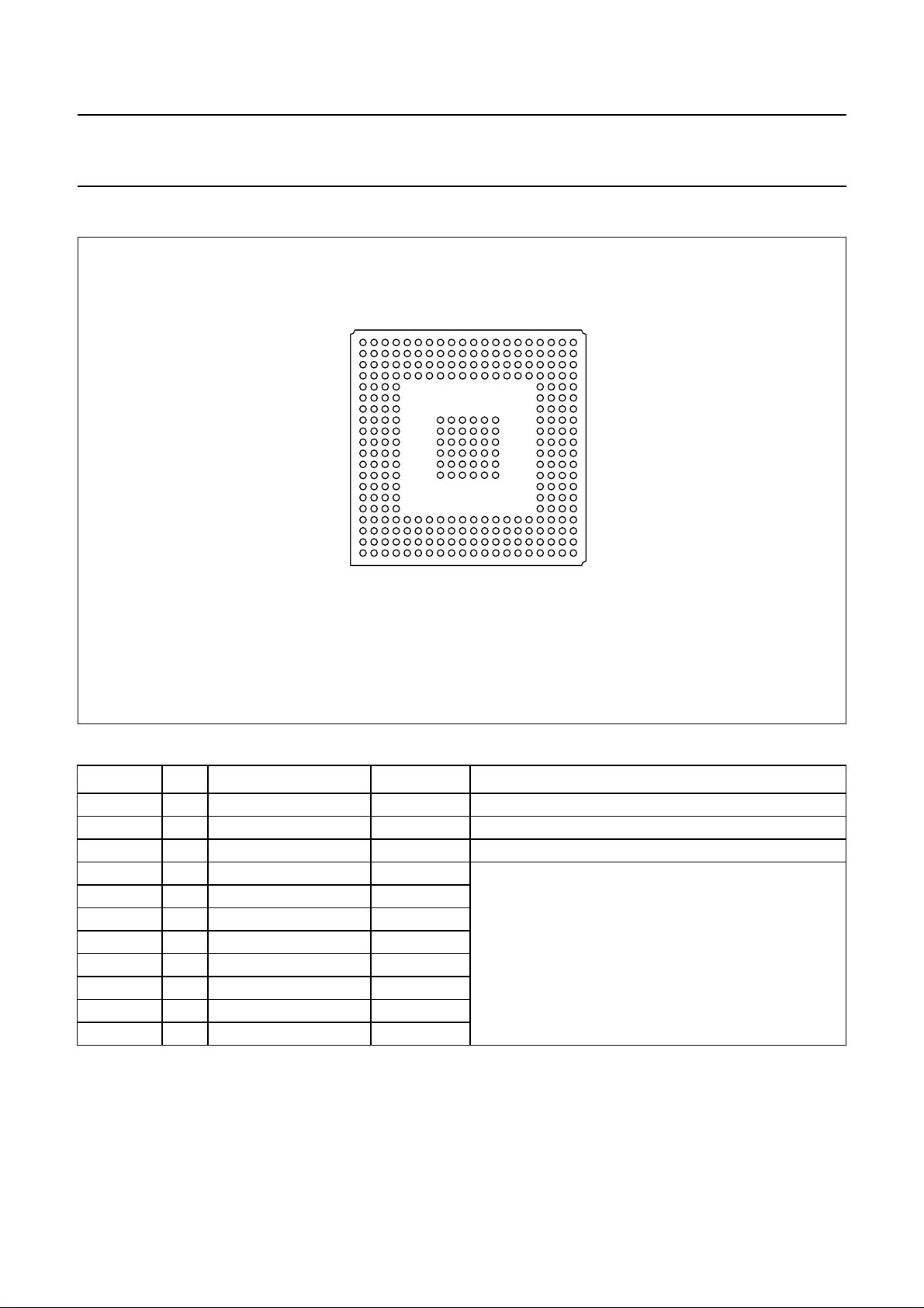
6 PINNING INFORMATION
handbook, halfpage
Y
W
V
U
T
R
P
N
M
L
K
J
H
G
F
E
D
C
B
A
SAA6721E
2468101214161820
135791113151719
MHB242
Fig.2 Pin configuration.
Table 1
SYMBOL PIN PORT I/O
(1)
DESCRIPTION
VCLK N1 RGB/YUV input input RGB/YUV sample clock
VVS M3 RGB/YUV input input RGB/YUV vertical sync
VHS M2 RGB/YUV input input RGB/YUV horizontal sync
VPA7 C7 RGB/YUV input input video input port A;
VPA6 A6 RGB/YUV input input
RGB port 0 red channel or YUV port luminance
VPA5 B6 RGB/YUV input input
VPA4 C6 RGB/YUV input input
VPA3 A5 RGB/YUV input input
VPA2 D5 RGB/YUV input input
VPA1 B5 RGB/YUV input input
VPA0 C5 RGB/YUV input input
1999 May 11 6
Page 7
Philips Semiconductors Preliminary specification
SXGA RGB to TFT graphics engine SAA6721E
SYMBOL PIN PORT I/O
VPB7 A4 RGB/YUV input input video input port B;
VPB6 B4 RGB/YUV input input
VPB5 C4 RGB/YUV input input
VPB4 A3 RGB/YUV input input
VPB3 B3 RGB/YUV input input
VPB2 C3 RGB/YUV input input
VPB1 A2 RGB/YUV input input
VPB0 B2 RGB/YUV input input
VPC7 B1 RGB/YUV input input video input port C;
VPC6 C2 RGB/YUV input input
VPC5 C1 RGB/YUV input input
VPC4 D3 RGB/YUV input input
VPC3 D2 RGB/YUV input input
VPC2 D1 RGB/YUV input input
VPC1 E3 RGB/YUV input input
VPC0 E2 RGB/YUV input input
VPD7 E4 RGB/YUV input input video input port D;
VPD6 E1 RGB/YUV input input
VPD5 F3 RGB/YUV input input
VPD4 F2 RGB/YUV input input
VPD3 F1 RGB/YUV input input
VPD2 G3 RGB/YUV input input
VPD1 G2 RGB/YUV input input
VPD0 G4 RGB/YUV input input
VPE7 G1 RGB/YUV input input video input port E; RGB port 1 green channel
VPE6 H3 RGB/YUV input input
VPE5 H2 RGB/YUV input input
VPE4 H1 RGB/YUV input input
VPE3 J2 RGB/YUV input input
VPE2 J4 RGB/YUV input input
VPE1 J1 RGB/YUV input input
VPE0 K3 RGB/YUV input input
VPF7 K2 RGB/YUV input input video input port F; RGB port 1 blue channel
VPF6 K1 RGB/YUV input input
VPF5 L1 RGB/YUV input input
VPF4 L4 RGB/YUV input input
VPF3 L2 RGB/YUV input input
VPF2 L3 RGB/YUV input input
VPF1 M1 RGB/YUV input input
VPF0 M4 RGB/YUV input input
(1)
DESCRIPTION
RGB port 0 green channel or YUV port chrominance
RGB port 0 blue channel or YUV port chrominance
RGB port 1 red channel or YUV data qualifier port
(VPD7 = CREF clock gating signal;
VPD6 = HREF active horizontal video)
1999 May 11 7
Page 8
Philips Semiconductors Preliminary specification
SXGA RGB to TFT graphics engine SAA6721E
SYMBOL PIN PORT I/O
CLAMP N2 RGB/YUV input output clamp pulse for analog-to-digital converter
GAINC N3 RGB/YUV input output gain correction pulse for analog-to-digital converter
PCLK Y13 panel interface output panel clock
PVS V12 panel interface output panel vertical sync
PHS W12 panel interface output panel horizontal sync
PDE U12 panel interface output panel data enable
PAR7 P1 panel interface output panel port A red channel
PAR6 P4 panel interface output
PAR5 P2 panel interface output
PAR4 P3 panel interface output
PAR3 R1 panel interface output
PAR2 R2 panel interface output
PAR1 R3 panel interface output
PAR0 T1 panel interface output
PAG7 T4 panel interface output panel port A green channel
PAG6 T2 panel interface output
PAG5 T3 panel interface output
PAG4 U1 panel interface output
PAG3 U2 panel interface output
PAG2 V1 panel interface output
PAG1 V2 panel interface output
PAG0 W1 panel interface output
PAB7 Y1 panel interface output panel port A blue channel
PAB6 W2 panel interface output
PAB5 Y2 panel interface output
PAB4 V3 panel interface output
PAB3 W3 panel interface output
PAB2 Y3 panel interface output
PAB1 V4 panel interface output
PAB0 Y4 panel interface output
PBR7 V5 panel interface output panel port B red channel
PBR6 W5 panel interface output
PBR5 Y5 panel interface output
PBR4 V6 panel interface output
PBR3 W6 panel interface output
PBR2 Y6 panel interface output
PBR1 V7 panel interface output
PBR0 W7 panel interface output
(1)
DESCRIPTION
1999 May 11 8
Page 9

Philips Semiconductors Preliminary specification
SXGA RGB to TFT graphics engine SAA6721E
SYMBOL PIN PORT I/O
(1)
DESCRIPTION
PBG7 Y7 panel interface output panel port B green channel
PBG6 V8 panel interface output
PBG5 W8 panel interface output
PBG4 Y8 panel interface output
PBG3 V9 panel interface output
PBG2 W9 panel interface output
PBG1 U9 panel interface output
PBG0 Y9 panel interface output
PBB7 V10 panel interface output panel port B blue channel
PBB6 W10 panel interface output
PBB5 Y10 panel interface output
PBB4 Y11 panel interface output
PBB3 U11 panel interface output
PBB2 W11 panel interface output
PBB1 V11 panel interface output
PBB0 Y12 panel interface output
SCL V18 I
SDA W18 input/output I
SAD Y17 input I
2
C-bus interface input I2C-bus interface clock line
2
C-bus interface data line
2
C-bus address select: 0 = 74H, 1 = 76H
OVCLK Y16 overlay output overlay port clock
OVVS W16 overlay output overlay port vertical sync
OVHS V15 overlay output overlay port horizontal sync
OVACT V16 overlay input overlay port pixel active
OVA0 Y14 overlay input overlay port input pixel A
OVA1 V13 overlay input
OVA2 W13 overlay input
OVB0 Y15 overlay input overlay port input pixel B
OVB1 V14 overlay input
OVB2 W14 overlay input
MCLKO A17 memory interface output memory clock output
RAS A18 memory interface output memory Row Address Strobe (RAS) signal (active LOW)
CAS
memory interface output memory Column Address Strobe (CAS) signal
C17
(active LOW)
WE D16 memory interface output memory Write Enable (WE) signal (active LOW)
DQM T17 memory interface output memory data mask (active LOW)
1999 May 11 9
Page 10

Philips Semiconductors Preliminary specification
SXGA RGB to TFT graphics engine SAA6721E
SYMBOL PIN PORT I/O
A0 A20 memory interface output memory address bus
A1 C20 memory interface output
A2 D20 memory interface output
A3 E19 memory interface output
A4 F18 memory interface output
A5 E17 memory interface output
A6 E18 memory interface output
A7 C19 memory interface output
A8 C18 memory interface output
A9 D18 memory interface output
A10 B19 memory interface output
BA A19 memory interface output memory bank select
DQ0 M20 memory interface input/output memory data bus
DQ1 M19 memory interface input/output
DQ2 N20 memory interface input/output
DQ3 N19 memory interface input/output
DQ4 P19 memory interface input/output
DQ5 R19 memory interface input/output
DQ6 T20 memory interface input/output
DQ7 T19 memory interface input/output
DQ8 T18 memory interface input/output
DQ9 R18 memory interface input/output
DQ10 P18 memory interface input/output
DQ11 P17 memory interface input/output
DQ12 N18 memory interface input/output
DQ13 M18 memory interface input/output
DQ14 M17 memory interface input/output
DQ15 L19 memory interface input/output
DQ16 E20 memory interface input/output
DQ17 F20 memory interface input/output
DQ18 G20 memory interface input/output
DQ19 H20 memory interface input/output
DQ20 J20 memory interface input/output
DQ21 K19 memory interface input/output
DQ22 K20 memory interface input/output
DQ23 L20 memory interface input/output
DQ24 K17 memory interface input/output
DQ25 K18 memory interface input/output
DQ26 J19 memory interface input/output
DQ27 J18 memory interface input/output
DQ28 H19 memory interface input/output
(1)
DESCRIPTION
1999 May 11 10
Page 11
Philips Semiconductors Preliminary specification
SXGA RGB to TFT graphics engine SAA6721E
SYMBOL PIN PORT I/O
DQ29 H18 memory interface input/output memory data bus
DQ30 G18 memory interface input/output
DQ31 F19 memory interface input/output
DQ32 A12 memory interface input/output
DQ33 B12 memory interface input/output
DQ34 A13 memory interface input/output
DQ35 B13 memory interface input/output
DQ36 A14 memory interface input/output
DQ37 B14 memory interface input/output
DQ38 A15 memory interface input/output
DQ39 B15 memory interface input/output
DQ40 A16 memory interface input/output
DQ41 C15 memory interface input/output
DQ42 C14 memory interface input/output
DQ43 D14 memory interface input/output
DQ44 C13 memory interface input/output
DQ45 C12 memory interface input/output
DQ46 D12 memory interface input/output
DQ47 C11 memory interface input/output
DQ48 B7 memory interface input/output
DQ49 A7 memory interface input/output
DQ50 B8 memory interface input/output
DQ51 A8 memory interface input/output
DQ52 B9 memory interface input/output
DQ53 A9 memory interface input/output
DQ54 B10 memory interface input/output
DQ55 A10 memory interface input/output
DQ56 B11 memory interface input/output
DQ57 A11 memory interface input/output
DQ58 D10 memory interface input/output
DQ59 C10 memory interface input/output
DQ60 D9 memory interface input/output
DQ61 C9 memory interface input/output
DQ62 C8 memory interface input/output
DQ63 D7 memory interface input/output
TCLK U19 JTAG test controller input JTAG test controller clock; note 2
TRST W17 input JTAG test controller reset (active LOW); note 2
TDI U18 input JTAG test data input; note2
TMS V19 input JTAG test mode select; note 2
TDO W19 output JTAG test data output
(1)
DESCRIPTION
1999 May 11 11
Page 12
Philips Semiconductors Preliminary specification
SXGA RGB to TFT graphics engine SAA6721E
SYMBOL PIN PORT I/O
(1)
DESCRIPTION
CLK Y19 miscellaneous input system and panel clock
RST Y20 input system reset (active LOW)
INT Y18 output mode detection interrupt (active LOW)
MCLKI W20 input memory clock input
V
SSD
A1 −−digital ground supply
D4
D8
D13
D17
H4
H17
N4
N17
U4
U8
U13
U17
V
DDD
D6 −−digital supply voltage
D11
D15
F4
F17
K4
L17
R4
R17
U6
U10
U15
V
SS(PLL)
V
DD(PLL)
V17 −−ground supply for internal PLL circuitry
U16 −−supply voltage for internal PLL circuitry
n.c. B16 −−not connected
n.c. B17 −−not connected
n.c. B18 −−not connected
n.c. B20 −−not connected
n.c. C16 −−not connected
n.c. D19 −−not connected
n.c. G17 −−not connected
n.c. G19 −−not connected
n.c. J3 −−not connected
n.c. J17 −−not connected
1999 May 11 12
Page 13
Philips Semiconductors Preliminary specification
SXGA RGB to TFT graphics engine SAA6721E
SYMBOL PIN PORT I/O
(1)
DESCRIPTION
n.c. L18 −−not connected
n.c. P20 −−not connected
n.c. R20 −−not connected
n.c. U3 −−not connected
n.c. U5 −−not connected
n.c. U7 −−not connected
n.c. U14 −−not connected
n.c. U20 −−not connected
n.c. V20 −−not connected
n.c. W4 −−not connected
n.c. W15 −−not connected
Notes
1. Generally all inputs are 5 V tolerant TTL inputs. All outputs are CMOS, except the memory interface ports, which are
LVTTL compatible.
2. Connect to ground when not using the JTAG controller.
7 FUNCTIONAL DESCRIPTION
7.1 Data path
Input video data is sampled either as RGB data in single
pixels from only one ADC or in double pixels in interleaved
format from two ADCs. Alternatively the input interface can
sample interlaced or non-interlaced YUV data. The clock
for sampling the data will always be provided from external
circuitry. The video stream will be adapted from the input
frame rate to the output frame rate needed by the panel.
Therefore a frame buffer built of SDRAMs or SGRAMs is
used. If the panel supports the incoming frame rate from
the RGB port, the adaption can be done without external
memory. If the video stream is in interlaced format the
memory interface activates its de-interlacing unit.
If zooming must be performed the upscaler behind the
memory interface will be enabled. For downscaling the
downscaler in front of the memory interface in the data
path will be used. A colour correction can be done via a
look-up table. The resulting video stream can now be
positioned elsewhere in the output data stream by the
panning unit. If an external OSD controller is embedded
into the system, its OSD window will be put into the video
stream by the OSD overlay port. Additionally the internal
OSD will be inserted in the next stage. The temporal
dithering allows true colour pictures to be displayed on
high colour panels. The output interface provides the
timing and control signals necessary for the connected
panel.
7.2 System clocks
7.2.1 I
NPUT INTERFACE CLOCK (VCLK)
This clock is used for sampling the incoming RGB or YUV
data stream. In RGB mode this clock varies from
25 to 150 MHz in single ADC mode. If two ADCs are used
the RGB input clock is between 12.5 and 75 MHz. In YUV
mode the clock lies in the range of approximately 30 MHz.
The clocks are generated from external devices.
The RGB clock can be generated by the external ADCs or
an external video PLL. The YUV clock must be generated
by the video decoder which also provides the YUV video
data.
7.2.2 M
EMORY INTERFACE CLOCK (MCLKI)
The memory clock is the synchronous clock for the
external frame buffer. Depending on the bandwidth
needed by the application, and the connected SDRAM or
SGRAM devices, the clock varies from 83 to 125 MHz.
It can be generated internally by the PLL from the system
clock (CLK), or by an external quartz oscillator.
If the internal PLL is used, the memory clock frequency
can be derived from the following formula:
f_memory
f_system
----------------------- N
16×=
Where N = pre-divider ratio and f_system = clock at
pin CLK.
1999 May 11 13
Page 14
Philips Semiconductors Preliminary specification
SXGA RGB to TFT graphics engine SAA6721E
7.2.3 I2C-BUS INTERFACE CLOCK (SCL)
This clock drives the interface to the external
microcontroller. Its frequency range is from
100 kHz to 1 MHz.
7.2.4 S
YSTEM CLOCK (CLK)
This clock is used to drive the internal PLL. The frequency
range is from 24 to 50 MHz.
7.2.5 TFT
PANEL CLOCK (PCLK)
This clock is the timing reference for the panel.
The frequency is the same as the system clock, or it can
be generated from the internal PLL by using the following
formula:
f_tft
f_system
----------------------- N
32
×=
-----M
Where N = pre-divider ratio and M = post-divider ratio.
7.3 RGB input port
The RGB input port can operate in two modes; single pixel
mode (24 bits) and double pixel mode (48 bits). For single
pixel mode only ports VPA7 to VPA0, VPB7 to VPB0, and
VPC7 to VPC0 are internally sampled. For double pixel
mode two pixels must be provided at the RGB input port.
Therefore ports VPD7 to VPD0, VPE7 to VPE0, and
VPF7 to VPF0 are also needed.
The VPA/B/C ports are sampled on the rising edge of the
RGB input clock (VCLK), and the VPD/E/F ports on the
falling edge (see Fig.3).
The synchronization pulses from the graphics card are
used to identify the frame outline. The vertical
synchronization pulse is connected to pin VVS, and the
horizontal synchronization pulse is connected to pin VHS.
For calibrating the connected Analog-to-Digital Converter
(ADC) the SAA6721E delivers a clamp pulse at
pin CLAMP, and a gain correction pulse at pin GAINC
(see Fig.4).
The sample window of the RGB input port is controlled by
four counters; horizontal and vertical offset, and horizontal
and vertical window size.
The offset counters start at the inactive or second edge of
their corresponding synchronization signal.
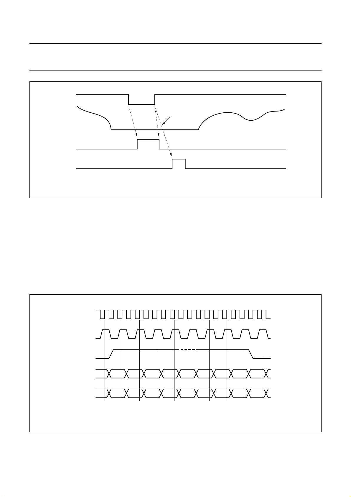
handbook, full pagewidth
VCLK
VPA/B/C
VPD/E/F
Fig.3 RGB input port timing.
1999 May 11 14
MHB243
Page 15
Philips Semiconductors Preliminary specification
SXGA RGB to TFT graphics engine SAA6721E
handbook, full pagewidth
VHS
RGB data
GAINC
CLAMP
Fig.4 Clamp and gain correction pulses.
7.4 YUV input port
The YUV input port supports interlaced video streams and
provides an easy connection to most common decoder
ICs. It consists of the luminance port VPA7 to VPA0, the
chrominance port VPB7 to VPB0, and eventually
VPC7 to VPC0, which are CCIR 601 level compatible
(Y: 16 to 235, and UV: 16 to 240).
Supported at this port are the formats YUV 4 : 1 : 1,
YUV4:2:2 and YUV 4:2:2 with CCIR 656 codes
(see Table 2).
blanking
MHB244
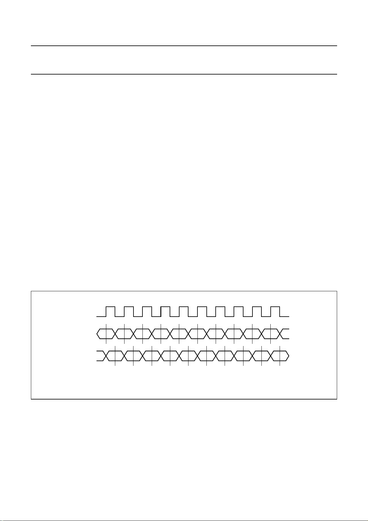
YUV 4:4:4 data can be applied at VPA7 to VPA0 (Y),
VPB7 to VPB0 (U), and VPC7 to VPC0 (V). Input data is
sampled with respect to the clock at pin VCLK if pin VPD7
(CREF) is asserted.
The start of active video data in a line is marked by the
rising edge at pin VPD6 (HREF) and the end of valid video
data is marked by the falling edge at pin VPD6. Figure 5
illustrates this at a YUV 4 :2:2 example.
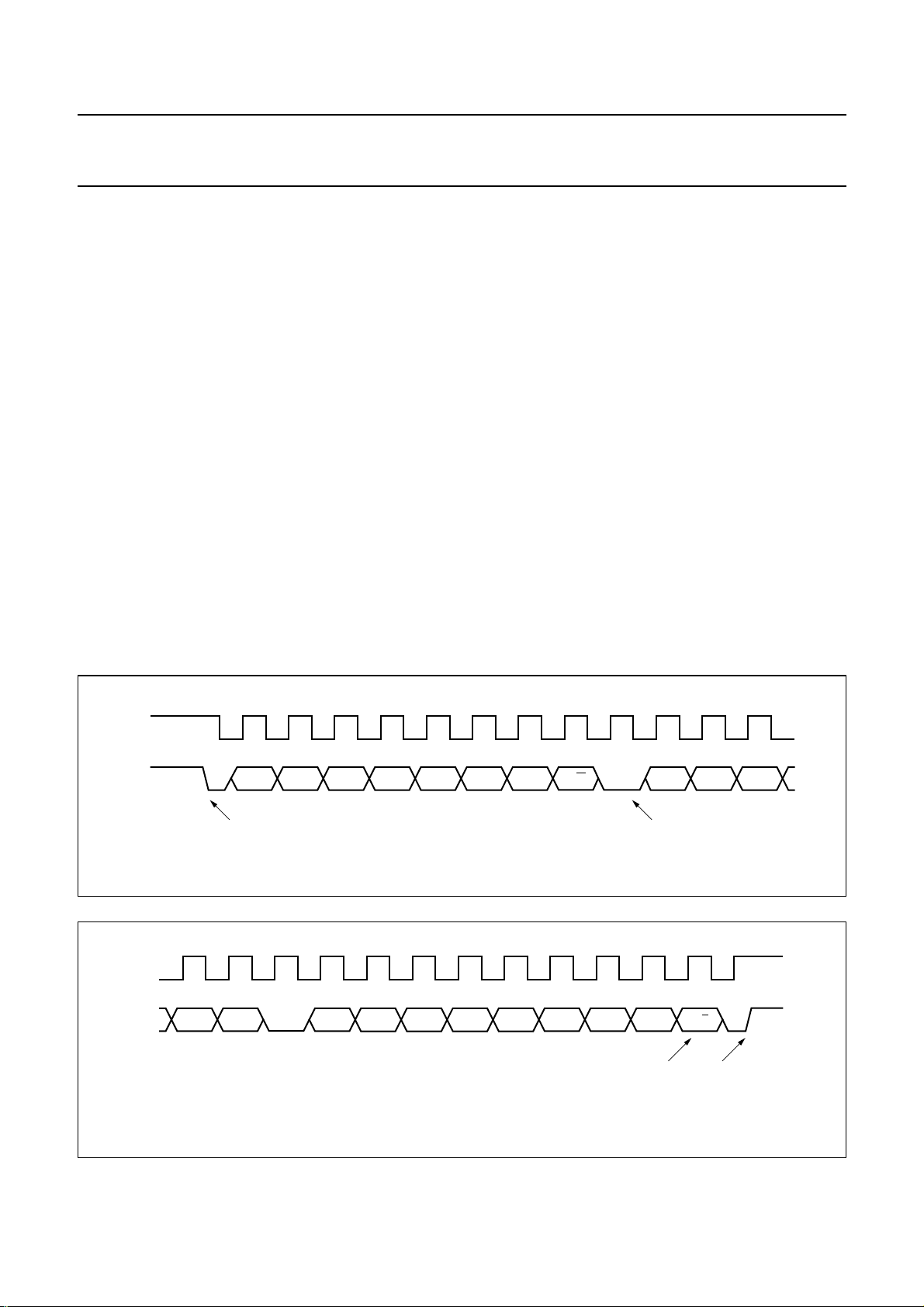
handbook, full pagewidth
VCLK
CREF
HREF
Y7 to Y0
UV7 to UV0
XX
XX
Y0 XXY719Y6Y5...Y3Y2Y1
U0 XXV718U718V716...V2U2V0
Fig.5 CREF and HREF timing.
1999 May 11 15
MHB245
Page 16

Philips Semiconductors Preliminary specification
SXGA RGB to TFT graphics engine SAA6721E
Table 2 YUV input formats
SIGNAL 4:1:1 FORMAT 4:2:2 FORMAT CCIR 656
Y7 Y07 Y17 Y27 Y37 Y07 Y17 U07 Y07 V07 Y17
Y6 Y06 Y16 Y26 Y36 Y06 Y16 U06 Y06 V06 Y16
Y5 Y05 Y15 Y25 Y35 Y05 Y15 U05 Y05 V05 Y15
Y4 Y04 Y14 Y24 Y34 Y04 Y14 U04 Y04 V04 Y14
Y3 Y03 Y13 Y23 Y33 Y03 Y13 U03 Y03 V03 Y13
Y2 Y02 Y12 Y22 Y32 Y02 Y12 U02 Y02 V02 Y12
Y1 Y01 Y11 Y21 Y31 Y01 Y11 U01 Y01 V01 Y11
Y0 Y00 Y10 Y20 Y30 Y00 Y10 U00 Y00 V00 Y10
UV7 U07 U05 U03 U01 U07 V07 X X X X
UV6 U06 U04 U02 U00 U06 V06 X X X X
UV5 V07 V05 V03 V01 U05 V05 X X X X
UV4 V06 V04 V02 V00 U04 V04 X X X X
UV3 XXXXU03V03XXXX
UV2 XXXXU02V02XXXX
UV1 XXXXU01V01XXXX
UV0 XXXXU00V00XXXX
Data frequency
1
⁄2VCLK
1
⁄2VCLK VCLK
For YUV 4 :4:4 the Y, U, and V components are available
in parallel.
If non-interlaced video data is applied, it is treated as odd
fields. Interlaced video data is sampled odd field,
even field, odd field, even field, etc. If there are equal
subsequent frames, only the first of these frames will be
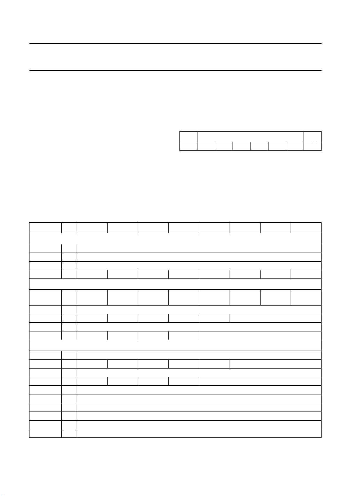
handbook, full pagewidth
VCLK
Y7 to Y0
FF ...Y1V0Y0U0SAV0000XX
Fig.6 CCIR 656 SAV code.
handbook, full pagewidth
VCLK
Y7 to Y0
U718 XXEAV0000FFY719V718Y718...
sampled. The decoding of odd and even fields is done with
HREF. In CCIR 656 data streams the included codes are
used for identifying even and odd frames, blanking and
active video data. The codes start with the byte sequence
FF 00 00, followed by the reference code byte;
see Figs 6 and 7.
MHB246
MHB247
Fig.7 CCIR 656 EAV code.
1999 May 11 16
Page 17
Philips Semiconductors Preliminary specification
SXGA RGB to TFT graphics engine SAA6721E
The CCIR 656 code byte contains vertical and horizontal
blanking as well as odd and even field information, the
protection bits P3 to P0 are ignored.
Table 3 CCIR 656 code byte
MSB LSB
76543210
1F
(2)
V
(3)
H
P3 P2 P1 P0
(1)
Notes
1. F = 0: odd field (field 1); F = 1: even field (field 2).
2. V = 0: in active field lines; V = 1: in field blanking.
3. H = 0: SAV (Start of Active Video);
H = 1: EAV (End of Active Video).
The sample window of the YUV input port is controlled by
four counters; horizontal and vertical offset, and horizontal
and vertical window size. The vertical offset counter starts
counting from the inactive or second edge of its
corresponding reference signal. The horizontal offset
counter starts with the active edge of the HREF signal.
7.5.2 DOUBLE PIXEL MODE
The double pixel mode is used for direct connection of TFT
panels with double pixel input. Both output ports are used.
The first pixel is applied at port A, and the second at port B.
7.6 Memory port
The memory port connects the SAA6721E to the external
frame buffer. This frame memory can be built from either
1M × 16 SDRAM or 256k × 32 SGRAM devices.
Supported are RAM devices with clock frequencies up to
125 MHz. This clock can be provided either by the internal
PLL, or externally be applied to pin MCLKI.
The memory data bus is split into 4 ports:
port 0 (DQ0 to DQ15), port 1 (DQ16 to DQ31),
port 2 (DQ32 to DQ47) and port 3 (DQ48 to DQ63).
To adapt the external memory to the needs of the
application by means of memory size and bandwidth, it is
possible to scale the external memory by using only the
number of subsequent ports needed to build up the frame
buffer and to achieve the memory bandwidth. As a second
step for bandwidth optimization several speed grades of
memory devices can be used.
7.5 TFT output port
The TFT output port consists of two pixel ports (A and B),
each containing red, green and blue colour information
with a resolution of 8 bits per colour. The first pixel port is
mapped to PAR7 to PAR0, PAG7 to PAG0, and
PAB7 to PAB0. The second port is mapped to
PBR7 to PBR0, PBG7 to PBG0, and PBB7 to PBB0.
The vertical and horizontal synchronization signals are
mapped to pins PVS and PHS. A data validation signal
framing visible pixels is available at pin PDE.
All of the above mentioned signals are synchronized to the
output clock at pin PCLK. The active edge of this clock is
programmable.
7.5.1 SINGLE PIXEL MODE
The single pixel mode is designed to support TFT panels
with single pixel input, and for direct connection of panel
link transmitters. Only the first pixel port PAR7 to PAR0,
PAG7 to PAG0, and PAB7 to PAB0 is used. The data is
applied at double the frequency in comparison to the
double pixel output mode.
7.6.1 SDRAM
MEMORY CONFIGURATION
SDRAMs are available in sizes from 16 Mbits. For this
application a wide data bus is required, so that at least
1M × 16 devices must be used. To achieve the desired
bandwidth, 2 to 4 devices must be used in parallel, which
results in a frame buffer size of 4 to 8 Mbytes. But only half
of this memory will be used by the SAA6721E.
The memory port of the SAA6721E can be divided into
4 SDRAM channels. Each channel is 16 bits wide, and
provides in High Speed Channel (HSC) mode with a
125 MHz memory clock and an effective bandwidth of
228 Mbits/s. A Medium Speed Channel (MSC) with a
100 MHz memory clock gives an effective bandwidth of
182 Mbits/s, 91% effective bandwidth assumed.
Table 4 gives the channel configuration for several input
and panel resolutions.
1999 May 11 17
Page 18

Philips Semiconductors Preliminary specification
SXGA RGB to TFT graphics engine SAA6721E
Table 4 SDRAM channel configurations
INPUT
RESOLUTION
SVGA (800 × 600) XGA (1024 × 768) SXGA (1280 × 1024)
60 Hz 75 Hz 60 Hz 75 Hz 60 Hz 75 Hz
Panel 2 Mbits frame buffer needed 3 Mbits frame buffer needed 4 Mbits frame buffer needed
XGA
SXGA
(1)
(2)
288 Mbits/s
bandwidth;
2 × HSC or
2 × MSC
307 Mbits/s
bandwidth;
2 × HSC or
2 × MSC
319 Mbits/s
bandwidth;
2 × HSC or
2 × MSC
337 Mbits/s
bandwidth;
2 × HSC or
2 × MSC
411 Mbits/s
bandwidth;
2 × HSC or
3 × MSC
435 Mbits/s
bandwidth;
2 × HSC or
3 × MSC
452 Mbits/s
bandwidth;
2 × HSC or
3 × MSC
476 Mbits/s
bandwidth;
3 × HSC or
3 × MSC
475 Mbits/s
bandwidth;
3 × HSC or
3 × MSC
624 Mbits/s
bandwidth;
3 × HSC or
4 × MSC
540 Mbits/s
bandwidth;
3 × HSC or
3 × MSC
705 Mbits/s
bandwidth;
4 × HSC or
4 × MSC
Notes
1. 36 MHz clock frequency.
2. 50 MHz clock frequency.
7.6.2 SGRAM MEMORY CONFIGURATION
SGRAM devices organized to 256k × 32 bits are available,
and feature the wide data bus for high speed applications.
With these devices a frame buffer can be built, without
wasting memory because of bandwidth. In case of
SGRAM usage, the memory data bus of the SAA6721E
Each channel gives, in HSC mode with 125 MHz clock
frequency, an effective bandwidth of 456 Mbits/s; and in
MSC mode, with 100 MHz clock speed, an effective
bandwidth of 364 Mbits/s.
Table 5 gives the channel configuration for several input
and panel resolutions.
can be split into 2 channels of 32 bits each.
Table 5 SGRAM channel configurations
INPUT
RESOLUTION
SVGA (800 × 600) XGA (1024 × 768) SXGA (1280 × 1024)
60 Hz 75 Hz 60 Hz 75 Hz 60 Hz 75 Hz
Panel 2 Mbits frame buffer needed 3 Mbits frame buffer needed 4 Mbits frame buffer needed
(1)
XGA
SXGA
(2)
288 Mbits/s
bandwidth;
1 × HSC or
1 × MSC
307 Mbits/s
bandwidth;
1 × HSC or
1 × MSC
319 Mbits/s
bandwidth;
1 × HSC or
1 × MSC
337 Mbits/s
bandwidth;
1 × HSC or
1 × MSC
411 Mbits/s
bandwidth;
1 × HSC or
2 × MSC
435 Mbits/s
bandwidth;
1 × HSC or
2 × MSC
452 Mbits/s
bandwidth;
1 × HSC or
2 × MSC
476 Mbits/s
bandwidth;
2 × HSC or
2 × MSC
475 Mbits/s
bandwidth;
2 × HSC or
2 × MSC
624 Mbits/s
bandwidth;
2 × HSC or
2 × MSC
540 Mbits/s
bandwidth;
2 × HSC or
2 × MSC
705 Mbits/s
bandwidth;
2 × HSC or
2 × MSC
Notes
1. 36 MHz clock frequency.
2. 50 MHz clock frequency.
1999 May 11 18
Page 19
Philips Semiconductors Preliminary specification
SXGA RGB to TFT graphics engine SAA6721E
7.7 I2C-bus interface
This serial interface consists of only two signals, the serial
clock line (SCL) and the serial data line (SDA).
The maximum supported frequency on this bus is 1 MHz.
Spikes with a maximum pulse length of 50 ns are
suppressed by the internal input filter.
The SAA6721E operates as a slave and cannot initiate
any data transfer, so the clock line is always input. Via the
data line, data is transmitted and received, so this pin must
be input/output. The SCL and SDA lines are driven by
open-drain stages and pull-up resistors. When a logic 0 is
applied, the bus is set to ground level via the output
buffers. When a logic 1 is applied, the output buffer
switches to 3-state and the pull-up resistors pull the bus up
to +5 V.
Data transfer changes on SDA are allowed only when SCL
is LOW. Data is sampled on the positive edge of SCL.
In Idle state the output buffers are in 3-state, and the bus
is HIGH. A data transfer must be initiated by an I2C-bus
master device. This is done by sending a START condition
when SDA changes from HIGH to LOW when SCL is HIGH
(see Fig.8).
The device address of the SAA6721E must then be sent
with the desired I/O direction.
If the SAA6721E reads its device address, it
acknowledges this by sending a single bit ACK to the
master. If write mode was selected, the master sends the
register address to be written and then the data bytes.
If read mode was selected, the SAA6721E sends the data
bytes starting from the last address accessed either by
write command or the next address at a read command.
All byte transfers are acknowledged from the receiving
device. The data transfer is aborted by sending a STOP
condition, when SDA changes from LOW to HIGH when
SCL is HIGH (see Fig.9).
If a new address has to be read or written, it is possible to
send a new START condition without a preceding STOP
condition. In this case the bus is still occupied by the
master, and it can initiate a new data transfer. This is
useful for read activities, where at first the register address
must be sent in write mode and after that a read command
will be sent to read data from this and following addresses.
handbook, full pagewidth
SCL
SDA
handbook, full pagewidth
SCL
SDA D7 D4D5D6D1 D0 ACK D2D3 A/A
START condition
A4 A1A2A3A6 A5 ACKR/W
A0 R5R7 R6
Fig.8 Start of a data transfer.
Fig.9 End of a data transfer.
acknowledge
D1 D0
acknowledge/
not acknowledge
MHB248
STOP condition
MHB249
1999 May 11 19
Page 20

Philips Semiconductors Preliminary specification
SXGA RGB to TFT graphics engine SAA6721E
If the data transfer was a read transfer and the master was
receiver, the master must not generate an acknowledge
before the STOP condition.
7.8 De-interlacing algorithms
The SAA6721E features several de-interlacing algorithms
for processing interlaced video data. Depending on the
algorithm different memory bandwidths and field
memories are needed.
7.8.1 STATIC MESH MODE
This mode allows de-interlacing without any image
processing and filtering. A field store for 2 fields is
necessary. De-interlacing is achieved by simply putting
lines together in the right order from the odd and even
fields in the field store and generating the output frame.
7.8.2 S
PATIAL FILTERING
The spatial filtering mode requires 2 field memories, but
only one memory is used at a time. For the calculation of
the whole frame from an odd field, the missing even lines
are interpolated from the odd lines before and after.
Processing of the even field is done in the same way.
7.8.3 T
EMPORAL FILTERING
The filtering algorithm needs 4 field memories and will be
applied temporally to subsequent fields.
The missing even line in an odd frame will be calculated by
interpolation from the corresponding even lines in the even
fields before and after. The odd line handling is done in the
same way.
7.9 Scaling algorithm
The SAA6721E features different scaling engines for up
and downscaling, for both horizontal and vertical
processing. The horizontal scaling engines are
independent from each other. The vertical scaling engines
share the line buffer, so they cannot operate in parallel.
7.9.1 U
PSCALING
The upscaling engine is used for enlarging the incoming
video frames. It can be used for zooming both RGB and
YUV video data. The magnification can be programmed
individually for horizontal and vertical scaling.
The maximum scaling factor for both directions is 64.
The implemented filter algorithm (see Fig.10) uses
interpolation with pixel enhancement, based on a free
programmable transition function. It is therefore possible
to define the transition between two calculated pixels to
obtain different sharpness characteristics. This transition
function must be defined in the 7 bits × 64 look-up table,
with a number ranging from 0 to 64. Different functions can
be programmed for horizontal and vertical scaling.
handbook, full pagewidth
AB
O
(1) The linear interpolation results in smoothing the sharp edges of the original picture if a pixel must be calculated.
(2) Some kind of1⁄xfunction results in sharper edges, because of the smaller transition interval.
(3) Phase correct pixel repetition can be done with this function.
intensity of
output pixel O
100% A,
0% B
0% A,
100% B
100% A,
0% B
(3)
(2)
0% A,
100% B
Fig.10 Interpolation function definition.
1999 May 11 20
(1)
MHB250
ratio between
input pixels A, B
Page 21
Philips Semiconductors Preliminary specification
SXGA RGB to TFT graphics engine SAA6721E
7.9.2 DOWNSCALING
The downscaling engine is used for reducing the incoming
RGB data stream, i.e. for displaying high resolution input
frames on panels with a smaller resolution. The scaling
ratio can be programmed independently for both horizontal
and vertical downscaling units. The algorithm uses pixel
accumulation, achieving a minimum scaling factor of1⁄64.
8 SYSTEM DESCRIPTION
8.1 Programming registers
The SAA6721E is a highly integrated device with many
features. To get the desired functionality and performance
it must be programmed correctly. In general, before
programming, the device must be switched to the internal
reset state to prevent unwanted functions while changing
the registers.
Table 7 Programming register overview
ADDRESS R/W D7 D6 D5 D4 D3 D2 D1 D0
State
0 R reserved
1 R reserved
2 R/W iic_test_register[7 to 0]
3R intr
After writing to all registers the internal reset can be
released. There are some registers (mainly offset
counters) that can be changed during data processing
without an internal reset. All accesses to the on screen
display can be done during data processing.
2
Table 6 I
MSB LSB
011101SADR/
Bit SAD = 0 the address is 74H, while bit SAD = 1 the
address is 76H.
Table 7 shows the programming model.
C-bus device address
W
RGB mode detection
4 R pos_
vsync
5 R v_lines[7 to 0]
6 R v_lines[10 to 8]
7 R h_clocks[7 to 0]
8 R h_clocks[11 to 8]
RGB auto-adjustment
9 W ref_line[7 to 0]
10 W ref_line[10 to 8]
11 W ref_pixel[7 to 0]
12 W ref_pixel[11 to 8]
13 W ref_colour[7 to 0]
14 R ref_pixel_red[7 to 0]
15 R ref_pixel_green[7 to 0]
16 R ref_pixel_blue[7 to 0]
17 R black_lines[7 to 0]
18 R black_pixels[7 to 0]
pos_
hsync
no_
vsync
no_
hsync
1999 May 11 21
Page 22

Philips Semiconductors Preliminary specification
SXGA RGB to TFT graphics engine SAA6721E
ADDRESS R/W D7 D6 D5 D4 D3 D2 D1 D0
19 R black_
pixels[8]
20 R non_black_lines[7 to 0]
21 R non_black_lines[10 to 8]
22 R non_black_pixels[7 to 0]
23 R non_black_pixels[11 to 8]
General configuration
24 W intr_clear single_
adc_mode
25 W yuv_clk_
Clock distribution
26 W por_mclk pre_div_
enable
27 W pre_div_clock_p_high[3 to 0] pre_div_clock_p_low[3 to 0]
28 W pre_div_clock_n_high[3 to 0] pre_div_clock_n_low[3 to 0]
29 W pre_div_clock_n_offs[3 to 0]
30 W post_div_clock_p_high[3 to 0] post_div_clock_p_low[3 to 0]
31 W post_div_clock_n_high[3 to 0] post_div_clock_n_low[3 to 0]
32 W post_div_clock_n_offs[3 to 0]
post_div_
enable
no_
memory_
mode
mux
pre_div_
half_clock
memory_
init
csm_
bypass
post_div_
half_clock
reset_
input_path
frc_on blank_
pll_enable pll_pclk pll_mclk
reset_
memory_
path
screen
reset_
proc_path
power_
down
Input interface
33 W rgb_interl_onin_form_onrgb_proc_onadc_
sample_
seq
34 W field_
reverse
35 W v_offset[7 to 0]
36 W v_offset[10 to 8]
37 W h_offset[7 to 0]
38 W h_offset[11 to 8]
39 W v_length[7 to 0]
40 W v_length[10 to 8]
41 W h_length[7 to 0]
42 W h_length[11 to 8]
43 W clamp_on[7 to 0]
44 W clamp_off[7 to 0]
45 W gainc_on_delay[7 to 0]
46 W gainc_off_delay[7 to 0]
yuv_field_mode
[1 and 0]
gainc_pol clamp_pol vs_pol hs_pol
yuv_input_mode
[1 and 0]
yuv_href_
pol
yuv_cref_
pol
1999 May 11 22
Page 23

Philips Semiconductors Preliminary specification
SXGA RGB to TFT graphics engine SAA6721E
ADDRESS R/W D7 D6 D5 D4 D3 D2 D1 D0
Colour correction
47 W red_prog green_
prog
48 W colour_index[7 to 0]
(1)
49 W
Memory interface/de-interlacing unit
50 W yuv422_
51 W burst_seq_length[3 to 0]
52 W SDRAM_burst_length_code[2 to 0] SDRAM_burst_length[3 to 0]
53 W CAS_latency[2 to 0] t_RCD[3 to 0]
54 W t_RRD[3 to 0] t_RP[3 to 0]
55 W t_WR[3 to 0] t_RC[3 to 0]
56 W field1_row[7 to 0]
57 W field1_row[10 to 8]
58 W field1_column[7 to 0]
59 W field2_row[7 to 0]
60 W field2_row[10 to 8]
61 W field2_column[7 to 0]
62 W field3_row[7 to 0]
63 W field3_row[10 to 8]
64 W field3_column[7 to 0]
65 W field4_row[7 to 0]
66 W field4_row[10 to 8]
67 W field4_column[7 to 0]
68 W frame_length[7 to 0]
69 W frame_length[10 to 8]
70 W line_length[7 to 0]
71 W line_length[11 to 8]
72 W blank_colour_red[7 to 0]
73 W blank_colour_green[7 to 0]
74 W blank_colour_blue[7 to 0]
colour_value[7 to 0]
data_width[1 and 0] deint_mode[1 and 0]
mode
blue_prog colour_
correction
_on
Scaler
75 W down_v_
scaler_
mem
76 W up_v_incr[7 to 0]
77 W up_v_incr[11 to 8]
78 W up_v_corr[6 to 0]
79 W up_h_incr[7 to 0]
1999 May 11 23
up_v_
coeff_prog
up_h_
coeff_prog
up_v_
scaler_on
up_h_
scaler_on
down_v_
scaler_on
down_h_
scaler_on
Page 24

Philips Semiconductors Preliminary specification
SXGA RGB to TFT graphics engine SAA6721E
ADDRESS R/W D7 D6 D5 D4 D3 D2 D1 D0
80 W up_h_incr[11 to 8]
81 W up_h_corr[6 to 0]
82 W down_v_incr[5 to 0]
83 W down_v_corr[6 to 0]
84 W down_h_incr[5 to 0]
85 W down_h_corr[6 to 0]
86 W coeff_index[5 to 0]
87 W
Panning unit
88 W pic_v_offset[7 to 0]
89 W pic_v_offset[10 to 8]
90 W pic_h_offset[7 to 0]
91 W pic_h_offset[11 to 8]
92 W out_v_size[7 to 0]
93 W out_v_size[10 to 8]
94 W out_h_size[7 to 1] 0
95 W out_h_size[11 to 8]
96 W border_colour_red[7 to 0]
97 W border_colour_green[7 to 0]
98 W border_colour_blue[7 to 0]
(1)
coeff_value[6 to 0]
OSD overlay port
99 W ovl_clk_
pol
100 W ovl_hs_start[7 to 0]
101 W ovl_hs_start[10 to 8]
102 W ovl_hs_length[7 to 0]
103 W ovl_hs_length[10 to 8]
104 W ovl_hs_latency[7 to 0]
105 W ovl_h_length[7 to 0]
106 W ovl_h_length[10 to 8]
107 W ovl_v_offset[7 to 0]
108 W ovl_v_offset[10 to 8]
109 W ovl_v_length[7 to 0]
110 W ovl_v_length[10 to 8]
111 W ovl_vs_start[7 to 0]
112 W ovl_vs_start[10 to 8]
113 W ovl_colour0_red[7 to 0]
114 W ovl_colour0_green[7 to 0]
115 W ovl_colour0_blue[7 to 0]
ovl_act_
pol
ovl_vs_
pol
ovl_hs_
pol
clk_
gating_on
sample_
edge
ovl_
syncs_
active
ovl_
insert_
active
1999 May 11 24
Page 25

Philips Semiconductors Preliminary specification
SXGA RGB to TFT graphics engine SAA6721E
ADDRESS R/W D7 D6 D5 D4 D3 D2 D1 D0
116 W ovl_colour1_red[7 to 0]
117 W ovl_colour1_green[7 to 0]
118 W ovl_colour1_blue[7 to 0]
119 W ovl_colour2_red[7 to 0]
120 W ovl_colour2_green[7 to 0]
121 W ovl_colour2_blue[7 to 0]
122 W ovl_colour3_red[7 to 0]
123 W ovl_colour3_green[7 to 0]
124 W ovl_colour3_blue[7 to 0]
125 W ovl_colour4_red[7 to 0]
126 W ovl_colour4_green[7 to 0]
127 W ovl_colour4_blue[7 to 0]
128 W ovl_colour5_red[7 to 0]
129 W ovl_colour5_green[7 to 0]
130 W ovl_colour5_blue[7 to 0]
131 W ovl_colour6_red[7 to 0]
132 W ovl_colour6_green[7 to 0]
133 W ovl_colour6_blue[7 to 0]
134 W ovl_colour7_red[7 to 0]
135 W ovl_colour7_green[7 to 0]
136 W ovl_colour7_blue[7 to 0]
On screen display
137 W zoom2 char_size osd_
138 W osd_v_offset[7 to 0]
139 W osd_v_offset[10 to 8]
140 W osd_h_offset[7 to 0]
141 W osd_h_offset[11 to 8]
142 W osd_v_size[5 to 0]
143 W osd_h_size[5 to 0]
144 W osd_fg_colour0_red[7 to 0]
145 W osd_fg_colour0_green[7 to 0]
146 W osd_fg_colour0_blue[7 to 0]
147 W osd_fg_colour1_red[7 to 0]
148 W osd_fg_colour1_green[7 to 0]
149 W osd_fg_colour1_blue[7 to 0]
150 W osd_fg_colour2_red[7 to 0]
151 W osd_fg_colour2_green[7 to 0]
152 W osd_fg_colour2_blue[7 to 0]
153 W osd_fg_colour3_red[7 to 0]
active
1999 May 11 25
Page 26

Philips Semiconductors Preliminary specification
SXGA RGB to TFT graphics engine SAA6721E
ADDRESS R/W D7 D6 D5 D4 D3 D2 D1 D0
154 W osd_fg_colour3_green[7 to 0]
155 W osd_fg_colour3_blue[7 to 0]
156 W osd_fg_colour4_red[7 to 0]
157 W osd_fg_colour4_green[7 to 0]
158 W osd_fg_colour4_blue[7 to 0]
159 W osd_fg_colour5_red[7 to 0]
160 W osd_fg_colour5_green[7 to 0]
161 W osd_fg_colour5_blue[7 to 0]
162 W osd_fg_colour6_red[7 to 0]
163 W osd_fg_colour6_green[7 to 0]
164 W osd_fg_colour6_blue[7 to 0]
165 W osd_fg_colour7_red[7 to 0]
166 W osd_fg_colour7_green[7 to 0]
167 W osd_fg_colour7_blue[7 to 0]
168 W osd_bg_colour0_red[7 to 0]
169 W osd_bg_colour0_green[7 to 0]
170 W osd_bg_colour0_blue[7 to 0]
171 W osd_bg_colour1_red[7 to 0]
172 W osd_bg_colour1_green[7 to 0]
173 W osd_bg_colour1_blue[7 to 0]
174 W osd_bg_colour2_red[7 to 0]
175 W osd_bg_colour2_green[7 to 0]
176 W osd_bg_colour2_blue[7 to 0]
177 W osd_bg_colour3_red[7 to 0]
178 W osd_bg_colour3_green[7 to 0]
179 W osd_bg_colour3_blue[7 to 0]
180 W osd_bg_colour4_red[7 to 0]
181 W osd_bg_colour4_green[7 to 0]
182 W osd_bg_colour4_blue[7 to 0]
183 W osd_bg_colour5_red[7 to 0]
184 W osd_bg_colour5_green[7 to 0]
185 W osd_bg_colour5_blue[7 to 0]
186 W osd_bg_colour6_red[7 to 0]
187 W osd_bg_colour6_green[7 to 0]
188 W osd_bg_colour6_blue[7 to 0]
189 W osd_bg_colour7_red[7 to 0]
190 W osd_bg_colour7_green[7 to 0]
191 W osd_bg_colour7_blue[7 to 0]
192 W osd_fg_
colour7_
transp
osd_fg_
colour6_
transp
osd_fg_
colour5_
transp
osd_fg_
colour4_
transp
osd_fg_
colour3_
transp
osd_fg_
colour2_
transp
osd_fg_
colour1_
transp
osd_fg_
colour0_
transp
1999 May 11 26
Page 27

Philips Semiconductors Preliminary specification
SXGA RGB to TFT graphics engine SAA6721E
ADDRESS R/W D7 D6 D5 D4 D3 D2 D1 D0
193 W osd_fg_
colour7_
alpha
194 W osd_bg_
colour7_
transp
195 W osd_bg_
colour7_
alpha
On screen display window
196 W cursor_row[5 to 0]
197 W cursor_column[5 to 0]
198 W char_appearance
[1 and 0]
199 W
(1)
osd_fg_
colour6_
alpha
osd_bg_
colour6_
transp
osd_bg_
colour6_
alpha
char_code[6 to 0]
osd_fg_
colour5_
alpha
osd_bg_
colour5_
transp
osd_bg_
colour5_
alpha
char_bg_colour[2 to 0] char_fg_colour[2 to 0]
osd_fg_
colour4_
alpha
osd_bg_
colour4_
transp
osd_bg_
colour4_
alpha
osd_fg_
colour3_
alpha
osd_bg_
colour3_
transp
osd_bg_
colour3_
alpha
osd_fg_
colour2_
alpha
osd_bg_
colour2_
transp
osd_bg_
colour2_
alpha
osd_fg_
colour1_
alpha
osd_bg_
colour1_
transp
osd_bg_
colour1_
alpha
osd_fg_
colour0_
alpha
osd_bg_
colour0_
transp
osd_bg_
colour0_
alpha
On screen display character matrix
200 W char_code[6 to 0]
201 W
TFT display interface
202 W vsync_pol hsync_pol de_pol clk_pol single_
203 W line_sync sync_de_
204 W h_len_blank[7 to 0]
205 W h_len_blank[10 to 8]
206 W h_len_border[7 to 0]
207 W h_len_border[10 to 8]
208 W h_len_active[7 to 0]
209 W h_len_active[10 to 8]
210 W v_end[7 to 0]
211 W v_end[10 to 8]
212 W v_start[7 to 0]
213 W v_start[10 to 8]
214 W v_active[7 to 0]
215 W v_active[10 to 8]
216 W h_vs_start[7 to 0]
217 W h_vs_start[10 to 8]
218 W h_vs_end[7 to 0]
219 W h_vs_end[10 to 8]
220 W h_hs_start[7 to 0]
221 W h_hs_start[10 to 8]
(1)
char_def[7 to 0]
act
out_if_
enable
blank_tft sync_
mode
blank_ctrl border_
ctrl
pixel_
output
active_ctrl
1999 May 11 27
Page 28

Philips Semiconductors Preliminary specification
SXGA RGB to TFT graphics engine SAA6721E
ADDRESS R/W D7 D6 D5 D4 D3 D2 D1 D0
222 W h_hs_end[7 to 0]
223 W h_hs_end[10 to 8]
224 W h_de_start[7 to 0]
225 W h_de_start[10 to 8]
226 W h_de_end[7 to 0]
227 W h_de_end[10 to 8]
228 W h_active_start[7 to 0]
229 W h_active_start[10 to 8]
230 W v_vs_end[7 to 0]
231 W v_vs_end[10 to 8]
232 W h_max_len[7 to 0]
233 W h_max_len[10 to 8]
Note
1. Register does not work with register address auto-increment, but with incrementing the address on which the
operation is performed.
Table 8 Detailed description of programming registers
NAME SUBADDRESS R/W DATA
State
IIC
TEST REGISTER
IIC test register 2 R/W D7 to D0
STATE REGISTER
Interrupt state 3 R D0
Interrupt active logic 0
Interrupt not active logic 1
RGB mode detection
S
YNC DETECT REGISTER
Hsync presence 4 R D0
Hsync present logic 0
Hsync not present logic 1
Vsync presence D1
Vsync present logic 0
Vsync not present logic 1
Hsync polarity D2
Negative Hsync logic 0
Positive Hsync logic 1
Vsync polarity D3
Negative Vsync logic 0
Positive Vsync logic 1
1999 May 11 28
Page 29

Philips Semiconductors Preliminary specification
SXGA RGB to TFT graphics engine SAA6721E
NAME SUBADDRESS R/W DATA
VERTICAL FRAME RESOLUTION
Number of lines between two Vsyncs 5 and 6 R D10 to D0
HORIZONTAL FRAME RESOLUTION
Number of clocks between two Hsyncs 7 and 8 R D11 to D0
RGB auto adjustment
EFERENCE LINE POSITION
R
Reference line for auto adjustment measurements 9 and 10 W D10 to D0
REFERENCE PIXEL POSITION
Reference pixel for auto adjustment measurements 11 and 12 W D11 to D0
REFERENCE COLOUR
Colour for selecting black or non-black pixels 13 W D7 to D0
REFERENCE PIXEL COLOUR RED COMPONENT
Red colour component of reference pixel 14 R D7 to D0
REFERENCE PIXEL COLOUR GREEN COMPONENT
Green colour component of reference pixel 15 R D7 to D0
REFERENCE PIXEL COLOUR BLUE COMPONENT
Blue colour component of reference pixel 16 R D7 to D0
BLACK LINES COUNTER
Number of black lines after Vsync 17 R D7 to D0
BLACK PIXELS COUNTER
Number of black pixels after Hsync 18 and 19 R D8 to D0
NON-BLACK LINES COUNTER
Number of non-black lines after Vsync 20 and 21 R D10 to D0
NON-BLACK PIXELS COUNTER
Number of non-black pixels after Hsync 22 and 23 R D11 to D0
1999 May 11 29
Page 30

Philips Semiconductors Preliminary specification
SXGA RGB to TFT graphics engine SAA6721E
NAME SUBADDRESS R/W DATA
General configuration
CONFIGURATION REGISTER 1
Processing reset state 24 W D0
Processing path not in reset state logic 0
Processing path in reset state logic 1
Memory reset state D1
Memory path not in reset state logic 0
Memory path in reset state logic 1
Input reset state D2
Input path not in reset state logic 0
Input path in reset state logic 1
External memory initialization D3
No external memory initialization logic 0
Start external memory initialization logic 1
External memory configuration D4
External memory present logic 0
No external memory present logic 1
External ADC configuration D5
2 ADCs connected logic 0
1 ADC connected logic 1
Interrupt acknowledge D6
No acknowledge logic 0
Reset interrupt output to logic 1 logic 1
C
ONFIGURATION REGISTER 2
Output interface Power-down mode 25 W D0
Normal processing logic 0
All outputs of output interface at LOW level logic 1
Blank screen D1
Normal data processing logic 0
Blank screen generation after memory interface logic 1
Output temporal dithering D2
No temporal dithering of output data stream logic 0
Temporal dithering of output data logic 1
Colour space conversion matrix D3
Conversion YUV to RGB enabled logic 0
Straight RGB processing enabled logic 1
YUV processing clock multiplexer D4
Clock will be applied at pin VCLK logic 0
Clock will be applied at pin MCLKI logic 1
1999 May 11 30
Page 31

Philips Semiconductors Preliminary specification
SXGA RGB to TFT graphics engine SAA6721E
NAME SUBADDRESS R/W DATA
Clock distribution
CLOCK MULTIPLEXING
Memory clock generation 26 W D0
Memory clock is taken from pin MCLKI logic 0
Memory clock is
Panel clock generation D1
Panel clock is equal system clock logic 0
Panel clock is generated by PLL clock and post-divider logic 1
PLL activation D2
PLL disabled logic 0
PLL enabled logic 1
PLL post-divider precision D3
1
⁄2 clock precision disabled logic 0
1
⁄2 clock precision enabled logic 1
PLL pre-divider precision D4
1
⁄2 clock precision disabled logic 0
1
⁄2 clock precision enabled logic 1
PLL post-divider activation D5
PLL post-divider disabled logic 0
PLL post-divider enabled logic 1
PLL pre-divider activation D6
PLL pre-divider disabled logic 0
PLL pre-divider enabled logic1
External memory clock multiplexer D7
Enable memory clock logic 0
Use system clock as external memory clock logic 1
P
RE-DIVIDER P-COUNTER
Pre-divider p-counter programming 27 W D7 to D0
PRE-DIVIDER N-COUNTER
Pre-divider n-counter programming 28 W D7 to D0
PRE-DIVIDER N-OFFSET
Pre-divider n-counter offset programming 29 W D3 to D0
POST-DIVIDER P-COUNTER
Post-divider p-counter programming 30 W D7 to D0
POST-DIVIDER N-COUNTER
Post-divider n-counter programming 31 W D7 to D0
POST-DIVIDER N-OFFSET
Post-divider n-counter offset programming 32 W D3 to D0
1
⁄2 PLL clock logic 1
1999 May 11 31
Page 32

Philips Semiconductors Preliminary specification
SXGA RGB to TFT graphics engine SAA6721E
NAME SUBADDRESS R/W DATA
Input interface
GENERAL PROGRAMMING
Hsync polarity 33 W D0
Hsync is active LOW, line starts at rising edge of pin VHS logic 0
Hsync is active HIGH, line starts at falling edge of pin VHS logic 1
Vsync polarity D1
Vsync is active LOW, line starts at rising edge of pin VVS logic 0
Vsync is active HIGH, line starts at falling edge of pin VVS logic 1
Clamp pulse polarity D2
Pulse is active LOW logic 0
Pulse is active HIGH logic 1
Gain correction pulse polarity D3
Pulse is active LOW logic 0
Pulse is active HIGH logic 1
ADC sample sequence D4
ADC 0 is sampled first after Hsync (video input port A, B, C) logic 0
ADC 1 is sampled first after Hsync (video input port D, E, F) logic 1
RGB/YUV processing mode D5
YUV processing enabled logic 0
RGB processing enabled logic 1
Input interface activation D6
No data sampling logic 0
Data sampling enabled logic 1
Interlaced RGB mode D7
Non-interlaced RGB processing logic 0
Interlaced RGB processing logic 1
1999 May 11 32
Page 33

Philips Semiconductors Preliminary specification
SXGA RGB to TFT graphics engine SAA6721E
NAME SUBADDRESS R/W DATA
INTERLACED MODE PROGRAMMING
YUV CREF polarity 34 W D0
YUV clock qualifier is active LOW logic 0
YUV clock qualifier is active HIGH logic 1
YUV HREF polarity D1
Active data qualifier is active LOW logic 0
Active data qualifier is active HIGH logic 1
YUV format D3 and D2
CCIR 656 D3 = 0 and D2 = 0
4:1:1 format D3 = 0 and D2 = 1
4:2:2 format D3 = 1 and D2 = 0
4:4:4 format D3 = 1 and D2 = 1
YUV field sampling mode D5 and D4
All incoming frames are captured D5 = 0 and D4 = 0
Capture alternating fields only D5 = 0 and D4 = 1
Capture odd fields only D5 = 1 and D4 = 0
Capture even fields only D5 = 1 and D4 = 1
Field reverse flag D6
Keep original odd field identification logic 0
Change field identification logic 1
V
ERTICAL SAMPLE OFFSET
Vertical sample offset from Vsync 35 and 36 W D10 to D0
HORIZONTAL SAMPLE OFFSET
Horizontal sample offset from Hsync 37 and 38 W D11 to D0
VERTICAL SAMPLE LENGTH
Vertical sample window length 39 and 40 W D10 to D0
HORIZONTAL SAMPLE LENGTH
Horizontal sample window length 41 and 42 W D11 to D0
CLAMP PULSE START
Start of clamp pulse after active edge of Hsync 43 W D7 to D0
CLAMP PULSE END
End of clamp pulse after active edge of Hsync 44 W D7 to D0
GAIN CORRECTION PULSE START DELAY
Delay of start of GAINC pulse from first edge of Hsync 45 W D7 to D0
GAIN CORRECTION PULSE END DELAY
Delay of end of pulse GAINC from second edge of Hsync 46 W D7 to D0
1999 May 11 33
Page 34

Philips Semiconductors Preliminary specification
SXGA RGB to TFT graphics engine SAA6721E
NAME SUBADDRESS R/W DATA
Colour correction
PROGRAMMING SELECTOR, ACTIVATION
Colour correction activation 47 W D0
Straight colour processing logic 0
Colour substitution enabled logic 1
Blue component programming D1
Red component correction colour writing disabled logic 0
Red component correction colour writing enabled logic 1
Green component programming D2
Red component correction colour writing disabled logic 0
Red component correction colour writing enabled logic 1
Red component programming D3
Red component correction colour writing disabled logic 0
Red component correction colour writing enabled logic 1
C
OLOUR INDEX FOR LOOK-UP TABLE WRITING
Colour component look-up table index 48 W D7 to D0
COLOUR VALUE FOR LOOK-UP TABLE WRITING
Colour component substitution value 49 W D7 to D0
Memory interface/de-interlacing unit
G
ENERAL CONFIGURATION
De-interlacing mode 50 W D1 and D0
No de-interlacing D1 = 0 and D0 = 0
De-interlacing without filtering D1 = 0 and D0 = 1
De-interlacing with spatial filtering D1 = 1 and D0 = 0
De-interlacing with temporal filtering D1 = 1 and D0 = 1
External memory data bus width D3 and D2
32 bits (two 16-bit channels) D3 = 0 and D2 = 0
48 bits (three 16-bit channels) D3 = 0 and D2 = 1
64 bits (four 16-bit channels) D3 = 1 and D2 = 0
do not use D3 = 1 and D2 = 1
Internal data path width D4
RGB and YUV 4:4:4 processing logic 0
YUV 4:2:2, YUV 4:1:1 and CCIR 656 processing logic 1
A
CCESS BURST LENGTH
Number of bursts per read/write access to SDRAM 51 W D3 to D0
SDRAM BURST LENGTH
SDRAM burst length 52 W D3 to D0
SDRAM initialization code for burst length D6 to D4
1999 May 11 34
Page 35

Philips Semiconductors Preliminary specification
SXGA RGB to TFT graphics engine SAA6721E
NAME SUBADDRESS R/W DATA
SDRAM TIMING PARAMETER 1; SEE TABLE 14
Active to read or write delay (t
CAS latency (CL) in clocks D6 to D4
SDRAM
TIMING PARAMETER 2; SEE TABLE 14
Precharge command period (t
Active bank A to active band B command (t
SDRAM TIMING PARAMETER 3; SEE TABLE 14
Auto refresh, active command period (t
Write recovery time (t
) in clocks D7 to D4
WR
FIELD 1 START ADDRESS (ROW)
Start address of field 1 in external SDRAM memory (row) 56 and 57 W D10 to D0
IELD 1 START ADDRESS (COLUMN)
F
Start address of field 1 in external SDRAM memory (column) 58 W D7 to D0
IELD 2 START ADDRESS (ROW)
F
Start address of field 2 in external SDRAM memory (row) 59 and 60 W D10 to D0
IELD 2 START ADDRESS (COLUMN)
F
Start address of field 2 in external SDRAM memory (column) 61 W D7 to D0
IELD 3 START ADDRESS (ROW)
F
Start address of field 3 in external SDRAM memory (row) 62 and 63 W D10 to D0
F
IELD 3 START ADDRESS (COLUMN)
Start address of field 3 in external SDRAM memory (column) 64 W D7 to D0
IELD 4 START ADDRESS (ROW)
F
Start address of field 4 in external SDRAM memory (row) 65 and 66 W D10 to D0
IELD 4 START ADDRESS (COLUMN)
F
Start address of field 4 in external SDRAM memory (column) 67 W D7 to D0
UTPUT FRAME LENGTH
O
Vertical length of output frame after de-interlacing unit 68 and 69 W D10 to D0
OUTPUT LINE LENGTH
Horizontal length of output frame after de-interlacing unit 70 and 71 W D11 to D0
BLANK COLOUR RED COMPONENT DEFINITION
Red colour component for blank screen generation 72 W D7 to D0
BLANK COLOUR GREEN COMPONENT DEFINITION
Green colour component for blank screen generation 73 W D7 to D0
BLANK COLOUR BLUE COMPONENT DEFINITION
Blue colour component for blank screen generation 74 W D7 to D0
) in clocks 53 W D3 to D0
RCD
) in clocks 54 W D3 to D0
RP
) in clocks D7 to D4
RRD
) in clocks 55 W D3 to D0
RC
1999 May 11 35
Page 36

Philips Semiconductors Preliminary specification
SXGA RGB to TFT graphics engine SAA6721E
NAME SUBADDRESS R/W DATA
Scaler
SCALER CONFIGURATION
Horizontal downscaler activation 75 W D0
Horizontal downscaler disabled logic 0
Horizontal downscaler enabled logic 1
Vertical downscaler activation D1
Vertical downscaler disabled logic 0
Vertical downscaler enabled logic 1
Horizontal upscaler activation D2
Horizontal upscaler disabled logic 0
Horizontal upscaler enabled logic 1
Vertical upscaler activation D3
Vertical upscaler disabled logic 0
Vertical upscaler enabled logic 1
Horizontal upscaling transition function programming D4
Horizontal upscaling transition function writing disabled logic 0
Horizontal upscaling transition function writing enabled logic 1
Vertical upscaling transition function programming D5
Vertical upscaling transition function writing disabled logic 0
Vertical upscaling transition function writing enabled logic 1
Line memory usage D6
Line memory used by upscaling unit logic 0
Line memory used by downscaling unit logic 1
V
ERTICAL UPSCALE INCREMENT
Increment for vertical upscaling 76 and 77 W D11 to D0
VERTICAL UPSCALE CORRECTION
Fraction of vertical upscaling increment (1⁄
HORIZONTAL UPSCALE INCREMENT
Increment for horizontal upscaling 79 and 80 W D11 to D0
HORIZONTAL UPSCALE CORRECTION
Fraction of horizontal upscaling increment (1⁄
VERTICAL DOWNSCALE INCREMENT
Increment for vertical downscaling 82 W D5 to D0
VERTICAL DOWNSCALE CORRECTION
Fraction of vertical downscaling increment (1⁄
HORIZONTAL DOWNSCALE INCREMENT
Increment for horizontal downscaling 84 W D5 to D0
) 78 W D6 to D0
100
) 81 W D6 to D0
100
) 83 W D6 to D0
100
1999 May 11 36
Page 37

Philips Semiconductors Preliminary specification
SXGA RGB to TFT graphics engine SAA6721E
NAME SUBADDRESS R/W DATA
HORIZONTAL DOWNSCALE CORRECTION
Fraction of horizontal downscaling increment (1⁄
INDEX FOR COEFFICIENT TABLE WRITING
Transition function look-up table index 86 W D5 to D0
COEFFICIENT VALUE FOR LOOK-UP TABLE WRITING
Values of transition function 87 W D6 to D0
Panning unit
V
ERTICAL PICTURE OFFSET
Vertical input picture offset inside the output frame 88 and 89 W D10 to D0
HORIZONTAL PICTURE OFFSET
Horizontal input picture offset inside the output frame 90 and 91 W D11 to D0
VERTICAL OUTPUT FRAME LENGTH
Vertical output frame length 92 and 93 W D10 to D0
HORIZONTAL OUTPUT FRAME LENGTH
Horizontal output frame length 94 and 95 W D11 to D0
BORDER COLOUR RED COMPONENT DEFINITION
Red colour component for border generation 96 W D7 to D0
BORDER COLOUR GREEN COMPONENT DEFINITION
Green colour component for border generation 97 W D7 to D0
BORDER COLOUR BLUE COMPONENT DEFINITION
Blue colour component for border generation 98 W D7 to D0
) 85 W D6 to D0
100
1999 May 11 37
Page 38

Philips Semiconductors Preliminary specification
SXGA RGB to TFT graphics engine SAA6721E
NAME SUBADDRESS R/W DATA
OSD overlay port
GENERAL CONFIGURATION
OSD overlay port activation 99 W D0
Overlay information will not be inserted into data stream logic 0
Overlay information will be inserted into data stream logic 1
Sync pulse generation D1
No sync pulses will be generated logic 0
Sync pulses will be generated logic 1
Clock edge for sampling D2
Data sampling at falling edge of clock at pin OVCLK logic 0
Data sampling at rising edge of clock at pin OVCLK logic 1
Clock gating D3
OVCLK always enabled logic 0
OVCLK enabled only during internal active video processing logic 1
Horizontal sync polarity D4
Active LOW horizontal sync pulse at pin OVHS logic 0
Active HIGH horizontal sync pulse at pin OVHS logic 1
Vertical sync polarity D5
Active LOW vertical sync pulse at pin OVVS logic 0
Active HIGH vertical sync pulse at pin OVVS logic 1
Overlay port active pixel qualifier polarity D6
Active LOW qualifier signal at pin OVACT logic 0
Active HIGH qualifier signal at pin OVACT logic 1
Overlay port clock polarity D7
Sync pulse change with respect to falling edge at pin OVCLK logic 0
Sync pulse change with respect to rising edge at pin OVCLK logic 1
O
VERLAY HORIZONTAL SYNC START
Start of horizontal sync pulse with respect to left frame border 100 and 101 W D10 to D0
OVERLAY HORIZONTAL SYNC LENGTH
Length of horizontal sync pulse 102 and 103 W D10 to D0
OVERLAY HORIZONTAL SYNC LATENCY
Delay between start of horizontal sync and valid overlay data 104 W D7 to D0
OVERLAY WINDOW HORIZONTAL LENGTH
Horizontal length of overlay region 105 and 106 W D10 to D0
OVERLAY WINDOW VERTICAL OFFSET
Vertical offset of overlay region 107 and 108 W D10 to D0
OVERLAY WINDOW VERTICAL LENGTH
Vertical length of overlay region 109and 110 W D10 to D0
1999 May 11 38
Page 39

Philips Semiconductors Preliminary specification
SXGA RGB to TFT graphics engine SAA6721E
NAME SUBADDRESS R/W DATA
OVERLAY VERTICAL SYNC START
Start of vertical sync pulse with respect to top frame border 111 and 112 W D10 to D0
COLOUR 0 TO 7 RED COMPONENT DEFINITION
Red colour component for overlay colour 0 to 7 113, 116, 119,
122, 125, 128,
131 and 134
COLOUR 0 TO 7 GREEN COMPONENT DEFINITION
Green colour component for overlay colour 0 to 7 114, 117, 120,
123, 126, 129,
132 and 135
COLOUR 0 TO 7 BLUE COMPONENT DEFINITION
Blue colour component for overlay colour 0 to 7 115, 118, 121,
124, 127, 130,
133 and 136
WD7toD0
WD7toD0
WD7toD0
On screen display
ENERAL CONFIGURATION
G
OSD activation 137 W D0
OSD is not visible logic 0
OSD is visible logic 1
OSD character size D1
12 × 16 character matrix logic 0
24 × 24 character matrix logic 1
OSD zoom D2
No zooming of OSD window logic 0
Zoom by 2 of OSD window logic 1
OSD
WINDOW VERTICAL OFFSET
Vertical offset of OSD window from left frame border in pixel 138 and 139 W D10 to D0
OSD WINDOW HORIZONTAL OFFSET
Horizontal offset of OSD window from top frame border in pixel 140 and 141 W D11 to D0
OSD WINDOW VERTICAL SIZE
Vertical size of OSD window in characters 142 W D5 to D0
OSD WINDOW HORIZONTAL SIZE
Horizontal size of OSD window in characters 143 W D5 to D0
FOREGROUND COLOUR 0 TO 7 RED COMPONENT DEFINITION
Red colour component for foreground colour 0 to 7 144, 147, 150,
153, 156, 159,
162 and 165
WD7toD0
1999 May 11 39
Page 40

Philips Semiconductors Preliminary specification
SXGA RGB to TFT graphics engine SAA6721E
NAME SUBADDRESS R/W DATA
FOREGROUND COLOUR 0 TO 7 GREEN COMPONENT DEFINITION
Green colour component for foreground colour 0 to 7 145, 148, 151,
154, 157, 160,
163 and 166
FOREGROUND COLOUR 0 TO 7 BLUE COMPONENT DEFINITION
Blue colour component for foreground colour 0 to 7 146, 149, 152,
155, 158, 161,
164 and 167
BACKGROUND COLOUR 0 TO 7 RED COMPONENT DEFINITION
Red colour component for background colour 0 to 7 168, 171, 174,
177, 180, 183,
186 and 189
BACKGROUND COLOUR 0 TO 7 GREEN COMPONENT DEFINITION
Green colour component for background colour 0 to 7 169, 172, 175,
178, 181, 184,
187 and 190
BACKGROUND COLOUR 0 TO 7 BLUE COMPONENT DEFINITION
Blue colour component for background colour 0 to 7 170, 173, 176,
179, 182, 185,
188 and 191
FOREGROUND TRANSPARENT COLOUR DEFINITION
Foreground colour transparency 192 W D7 to D0
Foreground colour is not transparent logic 0
Foreground colour is transparent logic 1
F
OREGROUND ALPHA BLENDING COLOUR DEFINITION
Foreground colour alpha blending 193 W D7 to D0
Foreground colour is not alpha blendable logic 0
Foreground colour is alpha blendable logic 1
B
ACKGROUND TRANSPARENT COLOUR DEFINITION
Background colour transparency 194 W D7 to D0
Background colour is not transparent logic 0
Background colour is transparent logic 1
ACKGROUND ALPHA BLENDING COLOUR DEFINITION
B
Background colour alpha blending 195 W D7 to D0
Background colour is not alpha blendable logic 0
Background colour is alpha blendable logic 1
WD7toD0
WD7toD0
WD7toD0
WD7toD0
WD7toD0
1999 May 11 40
Page 41

Philips Semiconductors Preliminary specification
SXGA RGB to TFT graphics engine SAA6721E
NAME SUBADDRESS R/W DATA
On screen display window
CURSOR POSITION 1
Cursor row 196 W D5 to D0
URSOR POSITION 2
C
Cursor column 197 W D5 to D0
HARACTER APPEARANCE
C
Foreground colour code 198 W D2 to D0
Background colour code D5 to D3
Character appearance D7 and D6
Picture information will be overwritten by OSD data D7 = 0 and D6 = 0
Transparency of OSD transparent colours D7 = 0 and D6 = 1
1 : 1 alpha blending of OSD alpha colours D7 = 1 and D6 = 0
1 : 2 alpha blending of OSD alpha colours D7 = 1 and D6 = 1
C
HARACTER CODE
Code of character to be placed at cursor position 199 W D6 to D0
On screen display character matrix
C
HARACTER CODE
Code of character to be defined 200 W D6 to D0
CHARACTER PATTERN
Character definition pattern 201 W D7 to D0
TFT display interface
G
ENERAL CONFIGURATION 1
Output width 202 W D0
Double pixel output (48 bits) logic 0
Single pixel output (24 bits) logic 1
Output clock polarity D1
Data output with respect to falling edge of pin PCLK logic 0
Data output with respect to rising edge of pin PCLK logic 1
Data qualifier polarity D2
Active LOW pin PDE logic 0
Active HIGH pin PDE logic 1
Horizontal sync polarity D3
Active LOW horizontal sync at pin PHS logic 0
Active HIGH horizontal sync at pin PHS logic 1
Vertical sync polarity D4
Active LOW vertical sync at pin PVS logic 0
Active HIGH vertical sync at pin PVS logic 1
1999 May 11 41
Page 42

Philips Semiconductors Preliminary specification
SXGA RGB to TFT graphics engine SAA6721E
NAME SUBADDRESS R/W DATA
GENERAL CONFIGURATION 2
Line length controlling in active video region 203 W D0
Line length controlling disabled logic 0
Line length controlling enabled logic 1
Line length controlling in border region D1
Line length controlling disabled logic 0
Line length controlling enabled logic 1
Line length controlling in top blanking region D2
Line length controlling disabled logic 0
Line length controlling enabled logic 1
Output interface mode D3
Free running output interface timing (external SDRAM required) logic 0
Synchronous output interface timing (without external SDRAM) logic 1
Blanking mode D4
Normal operating mode logic 0
All data outputs are at LOW level (black colour) logic 1
Output interface enabling D5
Output interface disabled, no data processing logic 0
Output interface enabled, normal data processing logic 1
Data qualifier generation mode D6
Disable pulse generation at pin PDE during vertical syncs logic 0
Enable pulse generation at pin PDE during vertical syncs logic 1
Line synchronization D7
Normal mode logic 0
Do not use logic 1
H
ORIZONTAL LINE LENGTH IN BLANKING REGION
Horizontal line length in blanking region 204 and 205 W D10 to D0
HORIZONTAL LINE LENGTH IN BORDER REGION
Horizontal line length in border region 206and 207 W D10 to D0
HORIZONTAL LINE LENGTH IN ACTIVE VIDEO REGION
Horizontal line length in active video region 208 and 209 W D10 to D0
VERTICAL FRAME END
Vertical frame length 210 and 211 W D10 to D0
VERTICAL BORDER REGION START
Vertical start of border region 212 and 213 W D10 to D0
VERTICAL ACTIVE VIDEO REGION START
Vertical start of active video region 214 and 215 W D10 to D0
HORIZONTAL DELAY OF START OF VERTICAL SYNC
Horizontal start delay of vertical sync pulse at pin PVS 216 and 217 W D10 to D0
1999 May 11 42
Page 43

Philips Semiconductors Preliminary specification
SXGA RGB to TFT graphics engine SAA6721E
NAME SUBADDRESS R/W DATA
HORIZONTAL DELAY OF END OF VERTICAL SYNC
Horizontal end delay of vertical sync pulse at pin PVS 218and 219 W D10 to D0
HORIZONTAL SYNC PULSE START
Start of horizontal sync pulse at pin PHS 220 and 221 W D10 to D0
HORIZONTAL SYNC PULSE END
End of horizontal sync pulse at pin PHS 222 and 223 W D10 to D0
DATA QUALIFIER START
Start of border region and horizontal data qualifier at pin PDE 224 and 225 W D10 to D0
DATA QUALIFIER END
End of border region and horizontal data qualifier at pin PDE 226 and 227 W D10 to D0
HORIZONTAL ACTIVE REGION START
Start of horizontal active video region 228 and 229 W D10 to D0
VERTICAL SYNC PULSE END
Vertical sync pulse end at pin PVS 230 and 231 W D10 to D0
MAXIMUM HORIZONTAL LINE LENGTH
Maximum reachable line length for length controlling 232 and 233 W D10 to D0
8.2 Clock management
8.2.1 C
For normal operation the SAA6721E uses two clock
inputs; pin VCLK and pin CLK. VCLK is used as the
sample clock provided by the external ADCs or decoder.
The frequency and the sample edges of this clock depend
on the number of ADCs connected, or on the video dot
clock:
• 1 ADC mode: maximum VCLK frequency is 150 MHz
• 2 ADC mode: maximum VCLK frequency is 75 MHz.
The clock from pin CLK is used as an internal reference,
and it is the source clock for the internal PLL. The memory
clock MCLKO and panel clock PCLK are derived from the
PLL (see Fig.11):
MCLKO
PCLK
Where N = pre-divider ratio, M = post-divider ratio and
5 MHz
LOCK GENERATION AND MULTIPLEXING
CLK
16×=
----------N
CLK
32
×=
-----------
------
N
M
CLK
8MHz≤≤
----------N
It is possible to drive the memory clock output directly
without the internal PLL via pin MCLKI. To achieve this the
programming flag pll_mclk must be set to logic 0.
The same is possible for the panel output clock. Therefore
the system clock CLK is used directly. The system clock is
controlled by pll_pclk which must be set to logic 0.
1999 May 11 43
Page 44

Philips Semiconductors Preliminary specification
SXGA RGB to TFT graphics engine SAA6721E
handbook, full pagewidth
MCLKI
MCLKO
CLK
PRE-DIVIDER
PLL
÷ 2
× 32
POST-DIVIDER
PCLK
MHB251
Fig.11 Clock generator.
8.2.2 CLOCK DIVIDER
The pre- and post-dividers are implemented in such a way, that they support dividing ratios of 0.5 steps in an interval
from 1.5 to 10.5. All further dividing ratios are in steps of 1.0; see Fig.12 and Table 9.
Programming of the clock dividers must be done using the registers 26 to 32. It is necessary that the clock dividers must
be disabled before programming and be enabled afterwards. This can be done with pre_div_enable and
post_div_enable.
handbook, full pagewidth
CLK
CLK/4
CLK/4.5
CLK/5
CLK/5.5
Fig.12 Clock waveforms.
Table 9 Clock divider programming
RATIO
P-COUNTER
(HEX)
N-COUNTER
(HEX)
1.5 10 10 1 1
2.0 00 00 0 0
2.5 30 30 2 1
3.0 10 10 0 1
3.5 41 41 3 1
1999 May 11 44
N-OFFSET
COUNTER (HEX)
MHB252
HALF CLK
Page 45

Philips Semiconductors Preliminary specification
SXGA RGB to TFT graphics engine SAA6721E
RATIO
4.0 11 00 0 0
4.5 61 61 4 1
5.0 21 21 0 1
5.5 72 72 5 1
6.0 22 00 0 0
6.5 92 92 6 1
7.0 32 32 0 1
7.5 A3 A3 7 1
8.0 33 00 0 0
8.5 C3 C3 8 1
9.0 43 43 0 1
9.5 D4 D4 9 1
10.0 44 00 0 0
10.5 F4 F4 A 1
11.0 54 54 0 1
12.0 55 00 0 0
13.0 65 65 0 1
14.0 66 00 0 0
15.0 76 76 0 1
16.0 77 00 0 0
17.0 87 87 0 1
18.0 88 00 0 0
19.0 98 98 0 1
20.0 99 00 0 0
21.0 A9 A9 0 1
22.0 AA 00 0 0
23.0 BA BA 0 1
24.0 BB 00 0 0
25.0 CB CB 0 1
26.0 CC 00 0 0
27.0 DC DC 0 1
28.0 DD 00 0 0
29.0 ED ED 0 1
30.0 EE 00 0 0
31.0 FE FE 0 1
32.0 FF 00 0 0
P-COUNTER
(HEX)
N-COUNTER
(HEX)
N-OFFSET
COUNTER (HEX)
HALF CLK
1999 May 11 45
Page 46

Philips Semiconductors Preliminary specification
SXGA RGB to TFT graphics engine SAA6721E
8.3 RGB/YUV input interface
8.3.1 S
AMPLING MODE
The input interface allows sampling of RGB or YUV data.
Because of that two different modes must be supported:
RGB data sampling and YUV data sampling. The flag
rgb_proc_on selects RGB mode sampling if asserted.
If the flag is not asserted YUV data is selected.
Sampling of interlaced RGB data is enabled by
rgb_interl_on.
8.3.2 RGB
DATA SAMPLING
Sampling is done on the rising edge or on both edges of
VCLK depending on the number of ADCs.
The sample window is defined by v_offset, h_offset,
v_length, and h_length.
The offset counters start counting from the second edge of
their reference signals, i.e. VVS for vertical offset and VHS
for horizontal offset. Figure 13 shows the horizontal offset.
The polarities of the sync signals are given with vs_pol and
hs_pol. The vertical sample offset is given in lines and the
horizontal offset is measured in pixels. The width of the
sample window is defined by the length counters.
The vertical width is measured in lines and the horizontal
width in pixels, but only even pixel numbers are allowed.
Table 10 Clock relationships
NUMBER OF
ADCs
VCLK
VCLK
SAMPLE EDGE
1 dot clock positive
2
1
⁄2 dot clock both
In single ADC mode, with each VCLK clock, a pixel must
be sampled from port A. In dual ADC mode, at each VCLK
clock edge, a pixel must be sampled alternating from
port A or B. The flag adc_sample_seq selects from which
port data sampling starts after the active edge of the
horizontal synchronization pulse.
8.3.3 C
LAMP PULSE GENERATION
The clamp pulse is generated with respect to half the dot
clock. The counters values responsible for switching the
clamp pulse on or off are clamp_on and clamp_off. Both
start counting from the second edge of VHS. The polarity
of CLAMP is given with clamp_pol.
The sample clock for the ADCs is always VCLK, but in dual
ADC mode this clock is half the pixel clock. Because of
that, in dual ADC mode, both clock edges are used to
sample data by the ADCs.
handbook, full pagewidth
VHS
RGB data
n
Fig.13 RGB data sampling.
h_offset
h_length
3
4
2
1
0
5
MHB253
1999 May 11 46
Page 47

Philips Semiconductors Preliminary specification
SXGA RGB to TFT graphics engine SAA6721E
8.3.4 GAIN CORRECTION PULSE GENERATION
The GAINC signal is the delayed horizontal sync pulse (VHS). It is delayed with respect to half the dot clock. The first
edge of VHS is delayed by gainc_on_delay and the second edge by gainc_off_delay (see Fig.14). The polarity is
programmed by gainc_pol.
handbook, full pagewidth
VHS
clamp_off
clamp_on
RGB data
GAINC
gainc_off_delaygainc_on_delay
CLAMP
Fig.14 Gain adjustment and clamp pulse generation.
8.3.5 YUV DATA SAMPLING
In YUV mode the input interface receives digital YUV
encoded video data from an external video decoder.
The video data can be in 4 : 4 : 4, 4 : 2 : 2, 4 : 1 : 1, or
YUV 4:2:2 with CCIR 656 codes. For the 4 : 4 : 4,
4:2:2, and 4:1:1 formats the reference signals VVS
and VHS must be considered to identify the frames.
The polarity of these signals is programmable with vs_pol
and hs_pol. The region of valid video data and the start
point for the UV sequence is defined by HREF applied at
pin VPD6.
External reference signals are needed for sampling the
YUV 4:4:4, 4:2:2 and 4 :1:1 data. If CCIR 656 data
is to be sampled, all external reference signals are
ignored, because their information is coded into the data
stream. All information about active video, blanking and
field ID is taken from the CCIR 656 codes. The selection of
the input format is done by yuv_input_mode as shown in
Table 11.
MHB254
Table 11 YUV input modes
yuv_input_mode[1 and 0] DESCRIPTION
0 YUV 4:2:2 with
CCIR 656 codes
1 YUV 4:1:1
2 YUV 4:2:2
3 YUV 4:4:4
Data sampling occurs in relation to horizontal and vertical
offset counters, and horizontal and vertical length
counters. They are the same as for programming the RGB
input, v_offset, h_offset, v_length, and h_length. All offset
and length values are relative to the whole frame, and not
to odd or even fields (see Fig.15).
1999 May 11 47
Page 48

Philips Semiconductors Preliminary specification
SXGA RGB to TFT graphics engine SAA6721E
handbook, full pagewidth
8.3.5.1 Field capturing
odd line
even line
Vsync end
Fig.15 Line sampling.
8.3.5.2 YUV clocking
MHB255
line number
1
314
2
315
3
316
4
317
5
318
6
319
7
320
8
321
9
322
10
323
11
324
12
325
offset
0
1
2
3
4
5
6
7
8
9
10
Another problem that must be considered is frame
dropping. It is possible that the connected video source
only provides either odd or even frames, or that the video
source drops frames. Therefore the input interface must
process the incoming video stream in several ways, as
shown in Table 12.
Table 12 Field capture modes
yuv_field_mode[1 and 0] DESCRIPTION
0 all incoming frames are
captured
1 after an odd frame the next
even frame will be
captured, and vice versa
2 capture only odd frames
3 capture only even frames
VCLK, or alternatively the clock from MCLKI, is used for
clocking the input interface in YUV mode and the data path
behind the external clock. This second port will be used if
yuv_clk_mux is set to logic 1. The external clock is the
line-locked video clock from the video decoder. This clock
is gated by CREF and applied at pin VPD7. Data is only to
be sampled if this signal is asserted. Alternatively the
line-locked video clock divided by two can be used
(if provided by the decoder). In this event CREF must be
tied to logic 1 or logic 0 depending on its programmed
polarity.
1999 May 11 48
Page 49

Philips Semiconductors Preliminary specification
SXGA RGB to TFT graphics engine SAA6721E
8.4 Video mode and synchronization signal
detection
The SAA6721E can be used to build up multi-sync
systems using an external microcontroller. Therefore
information about the input resolution and timing are
provided (see Tables 7 and 8). The flags pos_vsync and
pos_hsync show the polarity of the synchronization signals
at VVS and VHS. If they are set to logic 1 they are active
HIGH, and their active edge is the falling edge. If these
flags are set to logic 0, they are active LOW.
For detecting Video Electronic Standard Association
(VESA) Power-down modes or a not connected input, the
presence of the synchronization signals will be detected:
it can be read via no_vsync, and no_hsync. These flags
are active HIGH. The timing of the applied RGB video input
can be taken from v_lines reporting the number of lines of
a full frame. The horizontal timing can be calculated from
h_clocks. This register shows the length of a line in
numbers of reference clock periods. The reference clock is
equal to the panel clock PCLK in double pixel output mode
(48 bits in parallel), or it is half the panel clock PCLK in
single pixel output mode (24 bits in parallel).
If one of the above mentioned flags or counters changes
its value, it can be assumed that a new graphics mode has
been applied. In this case an interrupt at pin
generated. This port is active LOW. The reset can be
cleared by writing a logic 1 to intr_clear at address 24.
For adjusting the RGB input interface to a new graphics
mode, the registers of the section RGB auto adjustment
are to be used. With this auto adjustment support it is
possible to measure the number of blanking pixels and
lines between the end of the synchronization pulses and
the active video. The horizontal and vertical back porch
blanking can be read out at black_pixels and black_lines.
The number of active pixels or lines will be reported from
non_black_pixels and non_black_lines. The first value
should be used for tuning the sample clocks PLL so that
this value corresponds to the number of pixels to be
sampled horizontally in this specific graphics mode.
To distinguish between blanking and active video
ref_colour is used. If the sample values of all three colour
components are below this value the pixel is treated as a
blanking pixel, otherwise it is treated as active video.
Additionally a reference pixel can be defined with ref_line
and ref_pixel. The R, G, and B components of this pixel are
sampled and available at ref_pixel_red, ref_pixel_green,
and ref_pixel_blue. They can be used for fine tuning the
external PLL in frequency and phase and for colour gain
adjustment.
INT will be
8.5 Memory interface and de-interlacer unit
The SAA6721E features a 64 bits wide synchronous
DRAM interface. Both SDRAM and SGRAM devices can
be used. There is no difference in programming when
using SDRAM or SGRAM devices. The only thing that
must be considered is the amount of frame buffer memory,
which must be enough for the specific application.
Depending on the kind of input data stream the memory
interface must be switched to YUV 4 : 2 : 2 or YUV4:1:1
mode by setting yuv422_mode to logic 1 to enable 16 bits
per pixel processing. If this flag is set to logic 0, 24 bits per
pixel are used which is needed for RGB and YUV 4 : 4 : 4
processing. If not the whole bandwidth of the 64 bits wide
data bus is needed, the data bus can be downsized to
48 or 32 bits. This is done with the parameter data_width,
see Table 13.
Table 13 Data bus width
data_width[1 and 0]
032
148
264
Since the different timing parameters of various RAM
device types are different, all important timing values are
programmable and must be set-up according to the used
RAM types.
To reach a high effective bandwidth all access to the
external memory is organized in bursts. The larger the
number of subsequent read or write accesses the higher
the effective bandwidth. An effective bandwidth of 91%
can be reached by doing 64 words burst accesses.
The RAM devices support a maximum internal burst
length of 8 words only, so 8 of these bursts must be run
subsequently. This can be programmed by setting up the
RAM with SDRAM_burst_length_code taken from the
specification data of the SDRAM or SGRAM. The memory
interface must be programmed to 64 words bursts by
programming the RAM burst length SDRAM_burst_length
to 8, and the number of these bursts in burst_seq_length
to 8. The internal structure of the SAA6721E is optimized
for 64 words bursts.
PROGRAMMED BUS WIDTH
(BITS)
1999 May 11 49
Page 50

Philips Semiconductors Preliminary specification
SXGA RGB to TFT graphics engine SAA6721E
8.5.1 MEMORY INTERFACE LIMITATIONS
The timing parameters of the memory access can be programmed to fulfil the timing restrictions of several SDRAM or
SGRAM devices. But there are some limitations, as shown in Table 14.
Table 14 Memory interface limitations
TIMING SYMBOL PARAMETER CONDITIONS
CAS latency Column Address Strobe (CAS)
MINIMUM VALUE
(CLOCK PERIODS)
≥2
latency
t
RCD
activate to command delay; Row
≥2
Address Strobe (RAS) to CAS delay
t
RRD
t
RP
t
WR
t
RC
SDRAM_burst_length must be supported by
RAS to RAS bank activity delay t
≠ t
RRD
RCD
t
RRD=tRCD
; proposal is
+1
≥3
RAS precharge time ≥3
write recovery time ≥1
RAS cycle time ≥3
≥2
SDRAM
burst_seq_length must be an even number ≥2
t
RSC
Register Set Cycle (RSC) mode time internally defined; cannot be
=8
changed
8.5.2 I
NITIALIZATION OF EXTERNAL MEMORY
All SGRAM and SDRAM devices must be powered-up and initialized correctly. The SAA6721E memory interface is
implemented to fulfil the INTEL PC100 SDRAM specification.
Table 15 shows the required programming steps to initialize the memory correctly.
Table 15 Memory initialization programming
STEP ACTION REGISTERS
1 SAA6721E Power-on reset −
2 set-up timing parameters 51 to 55
3 start memory initialization with setting memory_init 24
4 set-up all other parameters 50 to 74
5 release internal memory reset together with other internal resets 24
8.5.3 F
RAME AND FIELD MEMORY
The memory interface acts as a decoupling unit to adapt the different frame rates at the video input to the panel output.
The external memory is also used for the de-interlacing unit which reconstructs the frames from odd and even fields in
interlaced mode. The algorithm of de-interlacing can be selected by deint_mode (see Table 16).
1999 May 11 50
Page 51

Philips Semiconductors Preliminary specification
SXGA RGB to TFT graphics engine SAA6721E
Table 16 De-interlacing modes
deint_mode[1 and 0] ALGORITHM MEMORY NEEDS
0 no de-interlacing and no filtering 1 frame buffer
1 de-interlacing without filtering 2 field buffers
2 de-interlacing with spatial filtering 2 field buffers
3 de-interlacing with temporal filtering 4 field buffers
De-interlacing mode 0 must be selected for non-interlaced input of RGB or YUV. Only one memory area is needed,
whose start address must be programmed into field1_row and field1_column. Normally this should be logic 0 for both
values. All other modes need more than one memory area. So the other field start addresses must be programmed
(see Fig.16).
handbook, full pagewidth
field1_row/column
deint_mode 0
field1_row/column
ODD FIELD
field2_row/column
EVEN FIELD
deint_mode 1/2
field1_row/column
field2_row/column
field3_row/column
field4_row/column
MHB256
ODD FIELD
EVEN FIELD
ODD FIELD
EVEN FIELD
deint_mode 3
Fig.16 Memory usage for de-interlacing.
The memory interface addresses alternately the two banks of the SDRAM or SGRAM devices. So the memory needs for
the field stores must be calculated from the following formula:
field_memory_size[18 to 0] number_of_pixels
×=
bytes_per_pixel
----------------------------------------------------------------------2 data_bus_width (bytes)×
, where
• number_of_pixels depends on the input resolution and whether it is an odd or even field
• bytes_per_pixel is 2 for YUV 4:2:2 and YUV 4:1:1; 3for YUV 4:4:4 and RGB.
All memory addresses must be transformed into row and column addresses used by DRAMs. The column address is
formed by the 8 LSBs (field_memory_size[7 to 0]), and the row address by all the other address bits
(field_memory_size[18 to 8]). The column address must be aligned to the number of internal DRAM bursts, normally in
steps of 8 (0, 8, 16, etc.).
1999 May 11 51
Page 52

Philips Semiconductors Preliminary specification
SXGA RGB to TFT graphics engine SAA6721E
The values given in Table 17 can be used for frame
resolutions up to 720 × 576 pixels which complies to the
625 line/50 Hz mode.
Table 17 Field start address values
FIELD VALUE (HEX)
Field1 row/column 000/0
Field2 row/column 08D/0
Field3 row/column 100/0
Field4 row/column 180/0
8.5.4 FRAME RECOVERY
During de-interlacing and also in mode 0, output frames
with the right vertical and horizontal dimensions must be
generated. Since size information is not stored in the
external memory, the output frame resolution must be
programmed into the registers frame_length and
line_length. The first value gives the vertical resolution,
and the second the horizontal resolution in pixels. If no
downscaler is used, these values can be taken directly
from the input interface. If downscaling is activated, the
size of the de-interlacer output frame must be calculated
from the RGB input frame size divided by the downscaling
factors.
If no valid data stream is applied at the RGB/YUV input
interface, the de-interlacer is able to generate a picture by
itself. This will be enabled with blank_screen at
address 25. The colour of this frame is defined by
blank_colour_red, blank_colour_green, and
blank_colour_blue.
Setting up the desired downscaling ratios is achieved by
programming the scaling increments down_v_incr,
down_v_corr, and down_h_incr, down_h_corr. This must
be done for both vertical and horizontal scaling.
incr
number_of_output_pixels
------------------------------------------------------------------number_of_input_pixels
64 xx.yy=×=
Where xx is equivalent to down_v_incr or down_h_incr
1
⁄
and yy is the fraction of the result in
100
.
This is the value for programming the increment correction
values down_v_corr and down_h_corr.
Example: SXGA → XGA
Horizontal:
1024
------------ 1280
64× 51.20=
This means down_h_incr = 51 and down_h_corr = 20.
768
Vertical:
------------ 1024
64× 48.00=
This means down_v_incr = 48 and down_v_corr = 0.
8.6.2 U
PSCALING
The upscaler must be activated by up_v_scaler_on and
up_h_scaler_on. To use the line memory for upscaling,
down_v_scaler_mem must be set to logic 0. To set-up the
zoom factor, the scaling increments up_v_incr, up_v_corr,
up_h_incr, and up_h_corr must be programmed.
incr
number_of_output_pixels
------------------------------------------------------------------number_of_input_pixels
64 xx.yy=×=
Where xx is equivalent to up_v_incr or up_h_incr and yy is
1
⁄
the fraction of the result in
100
.
8.6 Scaling
Two different scaling units are implemented to perform
both up and downscaling. The downscaling engine, which
is located before the memory interface, and the upscaling
engine after the memory interface.
8.6.1 DOWNSCALING
If the downscaler is to be used, it must be enabled by
setting flags down_v_scaler_on and down_h_scaler_on.
For vertical scaling a line memory buffer is needed.
This memory must be switched to downscaling mode by
setting down_v_scaler_mem to logic 1 because only one
is available.
1999 May 11 52
This is the value for programming the increment correction
values up_v_corr and up_h_corr.
Example: XGA → SXGA
Horizontal:
1280
------------ 1024
64× 80.00=
This means up_h_incr = 80 and up_h_corr = 0.
Vertical:
1024
------------ 768
64× 85.33=
This means up_v_incr = 85 and up_v_corr = 33.
Page 53

Philips Semiconductors Preliminary specification
SXGA RGB to TFT graphics engine SAA6721E
8.6.3 UPSCALER TRANSITION FUNCTION
A special feature of the zooming algorithm is a free
programmable transition function which allows smoothing
or sharpening of the transition between pixels that have
been calculated.
This function will be stored in a look-up table, containing
64 words of 7 bits; thus a function of 64 points with a
resolution from 0 to 64 can be programmed.
Programming is performed using the registers coeff_index
and coeff_value. The first register defines the point of the
function, the second the value. Writing to register
coeff_value increments the value of coeff_index
automatically, so that the next point of the function is
addressed. Additionally no register increment will be
performed, so that subsequent I2C-bus write addresses
always have the same register coeff_value.
handbook, full pagewidth
pic_h_offset
8.7 Panning unit
If the scaled or non-scaled input frame does not fit into the
needed output frame, whether it is to large or to small, the
panning unit enlarges the input frame to the size of the
output frame. This is achieved by generating a border
region around the input frame, or it cuts the input frame
down to the size of the output frame. The position of the
top left pixel of the input frame inside the output frame
must be defined with pic_v_offset and pic_h_offset.
The output frame size must be programmed with
out_v_size and out_h_size (see Fig.17).
If the input frame is to large only the right and bottom part
will be cropped. The colour of the generated border region
must be set via border_colour_red, border_colour_green,
and border_colour_blue.
pic_v_offset
INPUT FRAME
pic_v_offset
pic_h_offset
OUTPUT FRAME
out_h_size
Fig.17 Picture positioning.
out_v_size
MHB257
1999 May 11 53
Page 54

Philips Semiconductors Preliminary specification
SXGA RGB to TFT graphics engine SAA6721E
8.8 Overlay port
8.8.1 O
VERLAY INSERTION
If ovl_syncs_active is HIGH, the vertical and horizontal
sync signals for the external OSD controller are generated.
The flag ovl_insert_active switches on the insertion of the
information at the overlay port provided by an external
OSD controller into the data stream at the position defined
by ovl_v_offset, ovl_hs_start, and ovl_hs_latency
(see Fig.18).
handbook, full pagewidth
ovl_hs_start
ovl_hs_latency
The incoming data from ports ovl0 and ovl1 is replaced by
the defined colour information and treated as a double
pixel, which will be inserted into the data stream if OVACT
is set. The pixel at port 0 is then the left pixel, and the pixel
at port 1 is the right pixel. The sampling of the ports ovl0
and ovl1 is done on the positive edge of OVCLK in the
event that sample_edge is asserted, otherwise on the
falling edge of OVCLK.
ovl_v_offset
ovl_h_length
ovl_v_length
ovl_vs_start
one line Vsync
OVERLAY
WINDOW
OUTPUT FRAME
MHB258
Fig.18 Overlay window positioning.
1999 May 11 54
Page 55

Philips Semiconductors Preliminary specification
SXGA RGB to TFT graphics engine SAA6721E
8.8.2 SYNC GENERATION
The start of the horizontal sync pulse is defined in
ovl_hs_start and the polarity in ovl_hs_pol. The sync
pulse length is defined in ovl_hs_length (see Fig.19). It is
possible to generate a Hsync pulse from one clock cycle
length up to longer than the horizontal overlay data.
The vertical sync pulse starts at ovl_vs_start and is
always one output frame line long.
handbook, full pagewidth
OVCLK
OVHS
OVA
OVB
ovl_hs_start
ovl_hs_latency
8.8.3 DATA SAMPLING
Data sampling from the two ports OVA and OVB starts
from the beginning of the horizontal sync pulse, but the
number of clocks defined in ovl_hs_latency will decide
when reading data from the overlay port will start
(see Fig.19). The end of the sync pulse is not important.
ovl_hs_length
ovl_h_length
O0 O2 O4 O6 O8
O1 O3 O5 O7 O9
OVACT
Fig.19 Hsync generation and data sampling (Hsync latency = 2).
8.8.4 OVCLK GATING
All of the above mentioned functions will only work during
internal processing of valid video data, and not during
internal blanking regions. This can give problems if the
overlay window is displayed at the left border of the picture
because the first pixels of a line will be processed due to
the internal pipeline structure. To overcome this, the
OVCLK can be gated to disable data processing by the
external OSD controller during internal blanking. Clock
gating is enabled by clk_gating_on.
8.9 Colour space matrix
The back-end processing of the SAA6721E and the TFT
panels require RGB video data. So the built-in colour
space matrix is used to convert video data from YUV
space into RGB space. It can be enabled by setting
csm_bypass to logic 0 (see general configuration section
of the programming register Table 7), otherwise the colour
space converter will be bypassed.
MHB259
8.10 Colour correction
The colour correction unit can be used to perform gamma
correction, change of brightness, and so on. This can be
achieved by means of a look-up table. Each colour
component value in an RGB pixel is used as a pointer into
this table. The value from the table will replace the
incoming colour.
Various tables exist for R, G, and B components.
Programming of a table must be performed using the
programming registers 47 to 49 (see the colour correction
section of the programming register Table 7). It must be
decided which component table should be written to
(red_prog, green_prog, blue_prog). In colour_index the
start address or the first incoming colour value for
programming must be written. Then subsequent writing to
colour_value fill the table. At this address the I
2
C-bus
address auto-increment stops, but the value programmed
into colour_index will be incremented. It is possible to write
to more than one table by enabling of programming
multiple colour components.
1999 May 11 55
Page 56

Philips Semiconductors Preliminary specification
SXGA RGB to TFT graphics engine SAA6721E
If the colour correction unit is switched to bypass mode
(when colour_correction_on is not asserted), the incoming
colours are used for further processing.
Writing to the colour correction table is possible during
data processing.
8.11 On screen display
8.11.1 OSD GENERALS
The implemented OSD is a character based window
system. It consists of a character matrix memory where all
character definitions are stored, and an OSD window
memory defining the OSD window’s contents. The OSD
window will be inserted into the video data stream if
osd_active is set to logic 1. Writing to these memories can
be done during data processing.
8.11.2 OSD
WINDOW
The OSD window contains the character, colour and
appearance information to be displayed. Such a definition
exists for each character position. A character can use one
of 8 different foreground and background colours. Some of
these colours can be defined as transparent colours where
the original picture information will be displayed instead,
as alpha blended colours where a 1 : 1 or 1 : 2 alpha
blending will be done between picture and OSD, or as
normal colours. Transparency or alpha blending effects
will be enabled or disabled for the single characters.
The size and outline of the visible OSD window can be
programmed as long as the internal memory meets the
needs. This memory is able to store information of
1152 characters information.
The programming registers osd_v_size and osd_h_size
define the OSD window size in characters. The window
position inside the output frame must be defined with
osd_v_offset and osd_h_offset (see Fig.20).
handbook, halfpage
osd_v_offset
osd_h_offset
osd_v_size
OSD
OUTPUT FRAME
osd_h_size
MHB260
Fig.20 OSD window positioning.
The OSD can be programmed to use a 24 × 24 character
matrix, or a 12 × 16 matrix. The first one should be used for
Kanji and the second for standard characters.
The selection of the font size is done by char_size.
A logic 1 selects 24 × 24 font, and a logic 0 the smaller
12 × 16 font. If the small 12 × 16 font is used, up to
128 different characters can be defined. Alternatively up to
42 characters of the larger 24 × 24 font can be used.
Table 18 gives some possible OSD settings.
1999 May 11 56
Page 57

Philips Semiconductors Preliminary specification
SXGA RGB to TFT graphics engine SAA6721E
Table 18 OSD window size
OSD WINDOW
OSD SIZE
32 × 16 768 × 384 384 × 256
40 × 20 960 × 480 480 × 320
48 × 24 1152 × 576 576 × 384
The whole OSD window can be zoomed in both directions
by a factor of two by setting zoom2 to logic 1. This results
in pixel doubling horizontally and vertically.
Each character can be displayed using 1 of 8 different
foreground and background colours. These sixteen
colours can be chosen from the full true colour palette with
8 bits per colour component. The definition of these
colours is in registers 144 to 191 (see OSD section of the
programming register Table 7). The first 8 colour entries
are used for foreground colours, and the second half is
used for defining the background colours. Registers
192 to 195 (see Table 7) decide the transparency and
alpha blending effects. If one of these effects is enabled for
a specific character, only the colours defined as
transparency or alpha blending colours will be used to
generate these effects.
Each character information in the OSD window memory
consists of 15 bits of information. This is given in
Tables 19 and 20.
Table 19 Character appearance definition
CHARACTER INFORMATION NUMBER OF BITS
Character code 7
Appearance 2
Background colour 3
Foreground colour 3
The character code is used to address the defined
characters inside the matrix memory.
The appearance bits decide about transparency and alpha
blending, and background and foreground colour are
indices to the colour definition registers.
RESOLUTION/PIXELS
24 × 24 12 × 16
Table 20 Colour effects
APPEARANCE
VALUE
0 OSD character colours are displayed
instead of the picture colours
1 OSD character colours defined as
transparency colours will be replaced
by the picture colours
2 OSD character colours defined as
alpha blending colours will be alpha
blended 1 : 1 with the picture colours
3 OSD character colours defined as
alpha blending colours will be alpha
blended 2 : 1 with the picture colours
To access a certain character position its coordinates must
be programmed into registers 196 (cursor_row) and 197
(cursor_column), see Table 7. After that, the colours and
appearance of the character must be defined in
address 198 (see Table 7). This definition is valid for all
further writes to register 199 (char_code), see Table 7.
After writing to this register the cursor position changes to
the next right position. At line end it wraps around to the
first left character in the line below. I2C-bus auto-increment
is not active at register 199 (see Table 7), so that
subsequent I2C-bus byte write accesses will define several
characters.
8.11.3 OSD
Two different font sizes are supported; 24 × 24 and
12 × 16 pixels. With the internal matrix memory
42 characters (24 × 24 pixels) can be defined, or
128 characters (16 × 12 pixels).
The definition of the characters is achieved by writing to
registers 200 and 201 (see Table 7). The first register
must be written to with the character code of the character
to be defined. Then the bytes with the pixel pattern must
be written to address 201 (see Table 7). The definition of a
character is done with 3 bytes per line at 24 × 24 font
(72 bytes per character), and with 3 bytes per 2 lines at
12 × 16 font (24 bytes per character), see Fig.21.
CHARACTER MATRIX
EFFECT
1999 May 11 57
Page 58

Philips Semiconductors Preliminary specification
SXGA RGB to TFT graphics engine SAA6721E
The second mode is synchronized to the input data, mainly
implemented to support the SAA6721E’s no memory
mode. In this mode the input data is sent directly to the
output interface, which must synchronize its output timing
to get the same frame rate as the input. Additionally it
starts generating vertical blanking and synchronization
handbook, halfpage
1 byte
(a)
(b)
MHB261
signals at pins PVS and PHS directly after releasing the
internal reset.
After the programmed top blanking the output interface
enlarges the last blanking line until data from the input
interface reaches the output interface. Because too long
lines cause counter overflows in the panels, a controlling
mechanism exists which changes the length of the
blanking, border and active lines according to the timing
requirements of the panel and the applied graphics mode.
This mode can be enabled by setting the programming
register sync_mode to logic 1, otherwise the first free
running mode will be selected.
a: 24 × 24 font definition.
b: 12 × 16 font definition.
Fig.21 Character matrix organization.
8.12 Temporal dithering (frame rate controller)
The SAA6721E is able to display true colour (8 bits per
colour) on high colour displays (6 bits per colour).
The algorithm used is temporal dithering. This feature can
be enabled by setting frc_on to logic 1 in the general
configuration register block (see Table 7).
8.13 Output interface
8.13.1 G
ENERAL
The output interface is the interface between the
SAA6721E and the TFT panel. Its timing parameters can
be programmed in a wide range to support panels of many
different manufacturers.
The output interface can operate in two different modes.
The length controlling the blanking, border and active
video region can be enabled by asserting blank_ctrl,
border_ctrl, and active_ctrl.
The output interface also supports a Power-down mode
which sets all output signals to logic 0. This will be
activated by the programming flag power_down
(see section general configuration Table 7).
For flicker free switching between different input modes,
the output interface is able to set all data outputs to the
panel to logic 0, resulting in a black picture. Even if during
programming and internal reset no synchronization pulses
for the panel are generated and the panel loses the last
picture information, the panel still displays black colour,
because this is its Idle state. To switch the output interface
into this mode blank_tft must be set.
To enable the panel interface it must be enabled with
out_if_enable. The interface supports single pixel (24 bits)
and double pixel (48 bits) output in parallel. The selection
between these two modes must be done with
single_pixel_output. The active clock edge at PCLK can
also be selected by clk_pol.
The first mode is the free running mode which is adapted
to the memory mode of the SAA6721E. In this mode the
output is independent from the input at the RGB/YUV input
interface. So the output frame generation can start directly
after releasing the internal reset. For getting a high frame
rate the output timing can be programmed to satisfy the
minimum timing requirements of the panel.
1999 May 11 58
Page 59

Philips Semiconductors Preliminary specification
SXGA RGB to TFT graphics engine SAA6721E
8.13.2 FRAME GENERATION
The output frame contains three main regions:
• Blanking region
• Border region
• Active video region.
The blanking region contains all front and back porch as
well as the synchronization intervals. The border region is
visible on the panel and is used for positioning the active
video region inside this visible area. To ensure a great
flexibility in the ‘sync to input’ mode there are 3 different
horizontal length counters (h_len_blank, h_len_border,
h_len_active) with independent length control
(see Fig.22).
handbook, full pagewidth
starting point
h_hs_endh_hs_start
A maximum value must be programmed in h_max_len
which is the upper limit for line lengthening during
activated control mechanism. In free running mode all
3 counters should be programmed with the same
minimum values.
If no border is needed, because the active video region
covers the visible area of the panel, the active video length
counters should point to the same positions as the border
length counters. Then the active video length counters
have a higher priority.
The border colour inserted by the output interface is the
same as the blank colour in the memory interface;
blank_colour_red, blank_colour_green,
blank_colour_blue.
h_len_border
PHS
v_vs_end
v_start
v_active
v_end
PVS
h_de_start
active video
border
blanking
h_active_start h_de_end
Fig.22 Output frame and timing.
h_len_blank
h_len_active h_max_len
MHB262
1999 May 11 59
Page 60

Philips Semiconductors Preliminary specification
SXGA RGB to TFT graphics engine SAA6721E
8.13.3 TIMING REFERENCE SIGNALS
The SAA6721E supports three timing reference signals to
drive the panels: PVS (vertical synchronization pulse),
PHS (horizontal synchronization pulse) and PDE (data
qualifier). The polarity of these signals is programmable.
To program high polarity the three programming registers
(vsync_pol, hsync_pol, de_pol) must be set to logic 1.
Sometimes panels require that no data qualifier signals
must be active during vertical synchronization.
The generation of PDE pulses during active PVS can be
switched off by de-asserting sync_de_inact.
The position and length of the horizontal synchronization
pulses in an output line must be programmed with
h_hs_start and h_hs_end. The vertical synchronization
pulse starts at line 0 and ends at v_vs_end. The horizontal
start offset in line 0 can be set-up with h_vs_start and the
horizontal end offset with h_vs_end.
The data qualifier PDE frames the display region that
should be visible on the panel horizontally. It will be
asserted at h_de_start and it will be de-asserted at
h_de_end. It frames both horizontal border and active
video region.
9 LIMITING VALUES
In accordance with the Absolute Maximum Rating System (IEC 134); all ground pins are connected together and all
supply pins are connected together.
SYMBOL PARAMETER CONDITIONS MIN. MAX. UNIT
V
DDD
V
DD(PLL)
V
n
∆V
SS
T
stg
T
amb
T
amb(bias)
V
es
digital supply voltage −0.5 +4.6 V
PLL supply voltage −0.5 +4.6 V
voltage at digital inputs and outputs outputs in 3-state −0.5 +5.5 V
voltage at digital output outputs active −0.5 V
voltage difference between V
SS(PLL)
and V
SS(D)
− 100 mV
DDD
+ 0.5 V
storage temperature −65 +150 °C
ambient temperature 0 70 °C
operating bias ambient temperature −10 +70 °C
electrostatic handling voltage for all pins note 1 −2+2kV
Note
1. Human body model: equivalent to discharging a 100 pF capacitor through a 1.5 kΩ resistor.
1999 May 11 60
Page 61

Philips Semiconductors Preliminary specification
SXGA RGB to TFT graphics engine SAA6721E
10 CHARACTERISTICS
= 3.0 to 3.6 V; V
V
DDD
DD(PLL)
SYMBOL PARAMETER CONDITIONS MIN. TYP. MAX. UNIT
Supplies
V
DDD
I
DDD
P
D
V
DD(PLL)
I
DD(PLL)
P
PLL
P
PLL + D
digital supply voltage 3.0 3.3 3.6 V
digital supply current − 600 tbf mA
digital power dissipation − 2 − W
PLL supply voltage 3.1 3.3 3.5 V
PLL supply current − tbf tbf mA
PLL power dissipation − tbf − W
digital plus PLL power
dissipation
Digital inputs
V
IL(SCL, SDA)
LOW-level input voltage
at pins SDA and SCL
V
IH(SCL, SDA)
HIGH-level input voltage
at pins SDA and SCL
V
IL(LVTTL)
LOW-level input voltage
at LVTTL pins
V
IH(LVTTL)
HIGH-level input voltage
at LVTTL pins
I
LI
C
i
input leakage current −−10 µA
input capacitance outputs at 3-state −−8pF
input capacitance at all
other inputs
= 3.1 to 3.5 V; T
=25°C; unless otherwise specified.
amb
− 2 − W
−0.5 − +0.3V
0.7V
DDD
−0.5 − +0.8 V
2.0 − V
−−5pF
− V
DDD
DDD
DDD
+ 0.5 V
+ 0.5 V
V
Digital outputs
V
OL(SDA)
V
OL(CMOS)
LOW-level output voltage
at pin SDA
LOW-level output voltage
SDA at 3 mA sink current −−0.4 V
SDA at 6 mA sink current −−0.6 V
at CMOS pins
V
OH(CMOS)
HIGH-level output
voltage at CMOS pins
V
OL(LVTTL)
LOW-level output voltage
at LVTTL pins
V
OH(LVTTL)
HIGH-level output
voltage at LVTTL pins
1999 May 11 61
−−0.4 V
2.4 −−V
−−0.4 V
0.85V
−−V
DDD
Page 62

Philips Semiconductors Preliminary specification
SXGA RGB to TFT graphics engine SAA6721E
11 TIMING CHARACTERISTICS
= 3.0 to 3.6 V; V
V
DDD
DD(PLL)
SYMBOL PARAMETER CONDITIONS MIN. TYP. MAX. UNIT
System clock input at pin CLK
f
CLK
clock frequency 24 − 70 MHz
δ duty factor 40 50 60 %
RGB/YUV sample clock input at pin VCLK
f
VCLK
clock frequency single ADC mode 25 − 150 MHz
δ duty factor 40 50 60 %
Input signals at pins VVS, VHS, VPA7 to VPA0, VPB7 to VPB0, VPC7 to VPC0, VPD7 to VPD0, VPE7 to VPE0,
and VPF7 to VPF0 with respect to signal at pin VCLK
t
su
t
h
set-up time −4.0 −−ns
hold time 7.0 −−ns
Output signals at pins CLAMP and GAINC with respect to signal at pin VCLK; note 1
t
h
t
PD
hold time 8 −−ns
propagation delay −−13 ns
Output clock to panel at pin PCLK
f
PCLK
clock frequency −−80 MHz
δ duty factor 40 50 60 %
= 3.1 to 3.5 V; T
=25°C; see Fig.23; unless otherwise specified.
amb
double ADC mode 12.5 − 75 MHz
Output signals at pins PVS, PHS, PDE, PAR7 to PAR0, PAG7 to PAG0, PAB7 to PAB0, PBR7 to PBR0,
PBG7 to PBG0, and PBB7 to PBB0 with respect to signal at pin PCLK; note 2
t
h
hold time
pins PVS, PHS and PDE −0.5 −−ns
all other pins 0 −−ns
t
PD
propagation delay
pins PVS, PHS and PDE −−1ns
all other pins −−3.5 ns
Overlay port clock output at pin OVCLK
f
OVCLK
clock frequency 80 MHz
δ duty factor 40 50 60 %
Input signals at pins OVACT, OVA2 to OVA0, and OVB2 to OVB0 with respect to signal at pin OVCLK
t
su(i)
t
h(i)
set-up time 6.0 −−ns
hold time −3.0 −−ns
Output signals at pins OVVS and OVHS with respect to signal at pin OVCLK; note 1
t
h(o)
t
PD(o)
hold time −1.0 −−ns
propagation delay −−1.0 ns
1999 May 11 62
Page 63

Philips Semiconductors Preliminary specification
SXGA RGB to TFT graphics engine SAA6721E
SYMBOL PARAMETER CONDITIONS MIN. TYP. MAX. UNIT
Memory port clock output; pin MCLKO
f
MCLKO
C
L
δ duty factor 40 50 60 %
Input signal at pin MCLKI with respect to signal at pin MCLKO; see Fig.24
f
MCLKI
δ duty factor 40 50 60 %
t
PD
Input signals at pins DQ63 to DQ0 with respect to the negative edge of signal at pin MCLKO
t
su
t
h
Output signals at pins DQ63 to DQ0,
signal at pin MCLKO; note 3
t
h
t
PD
frequency −−125 MHz
load capacitance −−20 pF
frequency −−125 MHz
propagation delay 6.5 10 ns
set-up time 6.0 −−ns
hold time −3.0 −−ns
RAS, CAS, WE, A10 to A0, and BA with respect to the negative edge of
hold time
pins DQ63 to DQ0 −1 −−ns
pins
RAS, CAS, WE,
0 −−ns
A10 to A0, and BA
propagation delay
pins DQ63 to DQ0 −−1.0 ns
pins RAS, CAS, WE,
−−1.0 ns
A10 to A0, and BA
Notes
1. CL= 15pF, Io= 2 mA and RL=2kΩ.
2. CL= 15pF, Io= 4 mA and RL=2kΩ.
3. CL= 10pF, Io= 4 mA and RL=2kΩ.
1999 May 11 63
Page 64

Philips Semiconductors Preliminary specification
SXGA RGB to TFT graphics engine SAA6721E
handbook, full pagewidth
t
: input set-up time; data input must be stable before active clock edge.
su(i)
t
: input hold time; data input must be stable after active clock edge.
h(i)
t
: output propagation delay; output data becomes stable with respect to active clock edge.
PD(o)
t
: output hold time; output data stays stable with respect to active clock edge.
h(o)
clock input
data input
data output
t
su(i)
t
h(o)
data
valid
t
h(i)
t
Fig.23 Data timing diagram.
data
transition
period
PD(o)
1.5 V
MHB490
handbook, full pagewidth
MCLKI
MCLKO
t
PD
Fig.24 Memory clock timing.
1999 May 11 64
1.5 V
MHB491
Page 65

Philips Semiconductors Preliminary specification
SXGA RGB to TFT graphics engine SAA6721E
12 APPLICATION INFORMATION
handbook, full pagewidth
VIDEO
PORT
VGA
PORT
SAA7113A
TDA8752
TDA8752
YUV
RGB
RGB
SDRAM
16 MBits
PANEL PORT
Fig.25 Test board.
SDRAM
16 MBits
SAA6721E
SDRAM
16 MBits
SDRAM
16 MBits
EEPROM
MICROCONTROLLER
P87C695
I2C-bus
USB
MHB263
1999 May 11 65
Page 66

Philips Semiconductors Preliminary specification
SXGA RGB to TFT graphics engine SAA6721E
13 PACKAGE OUTLINE
BGA292: plastic ball grid array package; 292 balls; body 27 x 27 x 1.75 mm
D
D
1
ball A1
corner
E
E
1
k
k
e
Y
W
V
U
T
R
P
N
M
L
K
J
H
G
F
E
D
C
B
A
2468101214161820
135791113151719
DIMENSIONS (mm are the original dimensions)
A
UNIT
mm
max.
2.46
A
0.70
0.50
1
1.85
1.62
bA
D
27.2
26.8
D
24.7
24.0
2
0.90
0.60
b
∅ w
0 10 20 mm
Ew
1
27.2
26.8
E
24.7
24.0
Z
D
M
Z
E
e
scale
4.0
3.9
v
0.35
0.3
0.15
1
1.27
vA
yek
Z
1.84
1.04
SOT489-1
A
2
A
A
1
detail X
A
y
X
Z
D
E
1.84
1.04
OUTLINE
VERSION
IEC JEDEC EIAJ
REFERENCES
SOT489-1
1999 May 11 66
EUROPEAN
PROJECTION
ISSUE DATE
98-05-06
Page 67

Philips Semiconductors Preliminary specification
SXGA RGB to TFT graphics engine SAA6721E
14 SOLDERING
14.1 Introduction to soldering surface mount
packages
This text gives a very brief insight to a complex technology.
A more in-depth account of soldering ICs can be found in
our
“Data Handbook IC26; Integrated Circuit Packages”
(document order number 9398 652 90011).
There is no soldering method that is ideal for all surface
mount IC packages. Wave soldering is not always suitable
for surface mount ICs, or for printed-circuit boards with
high population densities. In these situations reflow
soldering is often used.
14.2 Reflow soldering
Reflow soldering requires solder paste (a suspension of
fine solder particles, flux and binding agent) to be applied
to the printed-circuit board by screen printing, stencilling or
pressure-syringe dispensing before package placement.
Several methods exist for reflowing; for example,
infrared/convection heating in a conveyor type oven.
Throughput times (preheating, soldering and cooling) vary
between 100 and 200 seconds depending on heating
method.
Typical reflow peak temperatures range from
215 to 250 °C. The top-surface temperature of the
packages should preferable be kept below 230 °C.
If wave soldering is used the following conditions must be
observed for optimal results:
• Use a double-wave soldering method comprising a
turbulent wave with high upward pressure followed by a
smooth laminar wave.
• For packages with leads on two sides and a pitch (e):
– larger than or equal to 1.27 mm, the footprint
longitudinal axis is preferred to be parallel to the
transport direction of the printed-circuit board;
– smaller than 1.27 mm, the footprint longitudinal axis
must be parallel to the transport direction of the
printed-circuit board.
The footprint must incorporate solder thieves at the
downstream end.
• For packages with leads on four sides, the footprint must
be placed at a 45° angle to the transport direction of the
printed-circuit board. The footprint must incorporate
solder thieves downstream and at the side corners.
During placement and before soldering, the package must
be fixed with a droplet of adhesive. The adhesive can be
applied by screen printing, pin transfer or syringe
dispensing. The package can be soldered after the
adhesive is cured.
Typical dwell time is 4 seconds at 250 °C.
A mildly-activated flux will eliminate the need for removal
of corrosive residues in most applications.
14.3 Wave soldering
Conventional single wave soldering is not recommended
for surface mount devices (SMDs) or printed-circuit boards
with a high component density, as solder bridging and
non-wetting can present major problems.
To overcome these problems the double-wave soldering
method was specifically developed.
1999 May 11 67
14.4 Manual soldering
Fix the component by first soldering two
diagonally-opposite end leads. Use a low voltage (24 V or
less) soldering iron applied to the flat part of the lead.
Contact time must be limited to 10 seconds at up to
300 °C.
When using a dedicated tool, all other leads can be
soldered in one operation within 2 to 5 seconds between
270 and 320 °C.
Page 68

Philips Semiconductors Preliminary specification
SXGA RGB to TFT graphics engine SAA6721E
14.5 Suitability of surface mount IC packages for wave and reflow soldering methods
PACKAGE
WAVE REFLOW
(1)
BGA, SQFP not suitable suitable
SOLDERING METHOD
HLQFP, HSQFP, HSOP, SMS not suitable
(3)
PLCC
, SO, SOJ suitable suitable
LQFP, QFP, TQFP not recommended
SSOP, TSSOP, VSO not recommended
(2)
(3)(4)
(5)
suitable
suitable
suitable
Notes
1. All surface mount (SMD) packages are moisture sensitive. Depending upon the moisture content, the maximum
temperature (with respect to time) and body size of the package, there is a risk that internal or external package
cracks may occur due to vaporization of the moisture in them (the so called popcorn effect). For details, refer to the
Drypack information in the
“Data Handbook IC26; Integrated Circuit Packages; Section: Packing Methods”
.
2. These packages are not suitable for wave soldering as a solder joint between the printed-circuit board and heatsink
(at bottom version) can not be achieved, and as solder may stick to the heatsink (on top version).
3. If wave soldering is considered, then the package must be placed at a 45° angle to the solder wave direction.
The package footprint must incorporate solder thieves downstream and at the side corners.
4. Wave soldering is only suitable for LQFP, TQFP and QFP packages with a pitch (e) equal to or larger than 0.8 mm;
it is definitely not suitable for packages with a pitch (e) equal to or smaller than 0.65 mm.
5. Wave soldering is only suitable for SSOP and TSSOP packages with a pitch (e) equal to or larger than 0.65 mm; it is
definitely not suitable for packages with a pitch (e) equal to or smaller than 0.5 mm.
1999 May 11 68
Page 69

Philips Semiconductors Preliminary specification
SXGA RGB to TFT graphics engine SAA6721E
15 DEFINITIONS
Data sheet status
Objective specification This data sheet contains target or goal specifications for product development.
Preliminary specification This data sheet contains preliminary data; supplementary data may be published later.
Product specification This data sheet contains final product specifications.
Limiting values
Limiting values given are in accordance with the Absolute Maximum Rating System (IEC 134). Stress above one or
more of the limiting values may cause permanent damage to the device. These are stress ratings only and operation
of the device at these or at any other conditions above those given in the Characteristics sections of the specification
is not implied. Exposure to limiting values for extended periods may affect device reliability.
Application information
Where application information is given, it is advisory and does not form part of the specification.
16 LIFE SUPPORT APPLICATIONS
These products are not designed for use in life support appliances, devices, or systems where malfunction of these
products can reasonably be expected to result in personal injury. Philips customers using or selling these products for
use in such applications do so at their own risk and agree to fully indemnify Philips for any damages resulting from such
improper use or sale
2
17 PURCHASE OF PHILIPS I
Purchase of Philips I
components in the I2C system provided the system conforms to the I2C specification defined by
Philips. This specification can be ordered using the code 9398 393 40011.
C COMPONENTS
2
C components conveys a license under the Philips’ I2C patent to use the
1999 May 11 69
Page 70

Philips Semiconductors Preliminary specification
SXGA RGB to TFT graphics engine SAA6721E
NOTES
1999 May 11 70
Page 71

Philips Semiconductors Preliminary specification
SXGA RGB to TFT graphics engine SAA6721E
NOTES
1999 May 11 71
Page 72

Philips Semiconductors – a worldwide company
Argentina: see South America
Australia: 34 Waterloo Road, NORTH RYDE, NSW 2113,
Tel. +61 2 9805 4455, Fax. +61 2 9805 4466
Austria: Computerstr. 6, A-1101 WIEN, P.O. Box 213,
Tel. +43 1 60 101 1248, Fax. +43 1 60 101 1210
Belarus: Hotel Minsk Business Center, Bld. 3, r. 1211, Volodarski Str. 6,
220050 MINSK, Tel. +375 172 20 0733, Fax. +375 172 20 0773
Belgium: see The Netherlands
Brazil: see South America
Bulgaria: Philips Bulgaria Ltd., Energoproject, 15th floor,
51 James Bourchier Blvd., 1407 SOFIA,
Tel. +359 2 68 9211, Fax. +359 2 68 9102
Canada: PHILIPS SEMICONDUCTORS/COMPONENTS,
Tel. +1 800 234 7381, Fax. +1 800 943 0087
China/Hong Kong: 501 Hong Kong Industrial Technology Centre,
72 Tat Chee Avenue, Kowloon Tong, HONG KONG,
Tel. +852 2319 7888, Fax. +852 2319 7700
Colombia: see South America
Czech Republic: see Austria
Denmark: Sydhavnsgade 23, 1780 COPENHAGEN V,
Tel. +45 33 29 3333, Fax. +45 33 29 3905
Finland: Sinikalliontie 3, FIN-02630 ESPOO,
Tel. +358 9 615 800, Fax. +358 9 6158 0920
France: 51 Rue Carnot, BP317, 92156 SURESNES Cedex,
Tel. +33 1 4099 6161, Fax. +33 1 4099 6427
Germany: Hammerbrookstraße 69, D-20097 HAMBURG,
Tel. +49 40 2353 60, Fax. +49 40 2353 6300
Hungary: see Austria
India: Philips INDIA Ltd, Band Box Building, 2nd floor,
254-D, Dr. Annie Besant Road, Worli, MUMBAI 400 025,
Tel. +91 22 493 8541, Fax. +91 22 493 0966
Indonesia: PT Philips Development Corporation, Semiconductors Division,
Gedung Philips, Jl. Buncit Raya Kav.99-100, JAKARTA 12510,
Tel. +62 21 794 0040 ext. 2501, Fax. +62 21 794 0080
Ireland: Newstead, Clonskeagh, DUBLIN 14,
Tel. +353 1 7640 000, Fax. +353 1 7640 200
Israel: RAPAC Electronics, 7 Kehilat Saloniki St, PO Box 18053,
TEL AVIV 61180, Tel. +972 3 645 0444, Fax. +972 3 649 1007
Italy: PHILIPS SEMICONDUCTORS, Piazza IV Novembre 3,
20124 MILANO, Tel. +39 02 67 52 2531, Fax. +39 02 67 52 2557
Japan: Philips Bldg 13-37, Kohnan 2-chome, Minato-ku,
TOKYO 108-8507, Tel. +81 3 3740 5130, Fax. +81 3 3740 5077
Korea: Philips House, 260-199 Itaewon-dong, Yongsan-ku, SEOUL,
Tel. +82 2 709 1412, Fax. +82 2 709 1415
Malaysia: No. 76 Jalan Universiti, 46200 PETALING JAYA, SELANGOR,
Tel. +60 3 750 5214, Fax. +60 3 757 4880
Mexico: 5900 Gateway East, Suite 200, EL PASO, TEXAS 79905,
Tel. +9-5 800 234 7381, Fax +9-5 800 943 0087
Middle East: see Italy
Netherlands: Postbus 90050, 5600 PB EINDHOVEN, Bldg. VB,
Tel. +31 40 27 82785, Fax. +31 40 27 88399
New Zealand: 2 Wagener Place, C.P.O. Box 1041, AUCKLAND,
Tel. +64 9 849 4160, Fax. +64 9 849 7811
Norway: Box 1, Manglerud 0612, OSLO,
Tel. +47 22 74 8000, Fax. +47 22 74 8341
Pakistan: see Singapore
Philippines: Philips Semiconductors Philippines Inc.,
106 Valero St. Salcedo Village, P.O. Box 2108 MCC, MAKATI,
Metro MANILA, Tel. +63 2 816 6380, Fax. +63 2 817 3474
Poland: Ul. Lukiska 10, PL 04-123 WARSZAWA,
Tel. +48 22 612 2831, Fax. +48 22 612 2327
Portugal: see Spain
Romania: see Italy
Russia: Philips Russia, Ul. Usatcheva 35A, 119048 MOSCOW,
Tel. +7 095 755 6918, Fax. +7 095 755 6919
Singapore: Lorong 1, Toa Payoh, SINGAPORE 319762,
Tel. +65 350 2538, Fax. +65 251 6500
Slovakia: see Austria
Slovenia: see Italy
South Africa: S.A. PHILIPS Pty Ltd., 195-215 Main Road Martindale,
2092 JOHANNESBURG, P.O. Box 58088 Newville 2114,
Tel. +27 11 471 5401, Fax. +27 11 471 5398
South America: Al. Vicente Pinzon, 173, 6th floor,
04547-130 SÃO PAULO, SP, Brazil,
Tel. +55 11 821 2333, Fax. +55 11 821 2382
Spain: Balmes 22, 08007 BARCELONA,
Tel. +34 93 301 6312, Fax. +34 93 301 4107
Sweden: Kottbygatan 7, Akalla, S-16485 STOCKHOLM,
Tel. +46 8 5985 2000, Fax. +46 8 5985 2745
Switzerland: Allmendstrasse 140, CH-8027 ZÜRICH,
Tel. +41 1 488 2741 Fax. +41 1 488 3263
Taiwan: Philips Semiconductors, 6F, No. 96, Chien Kuo N. Rd., Sec. 1,
TAIPEI, Taiwan Tel. +886 2 2134 2886, Fax. +886 2 2134 2874
Thailand: PHILIPS ELECTRONICS (THAILAND) Ltd.,
209/2 Sanpavuth-Bangna Road Prakanong, BANGKOK 10260,
Tel. +66 2 745 4090, Fax. +66 2 398 0793
Turkey: Yukari Dudullu, Org. San. Blg., 2.Cad. Nr. 28 81260 Umraniye,
ISTANBUL, Tel. +90 216 522 1500, Fax. +90 216 522 1813
Ukraine: PHILIPS UKRAINE, 4 Patrice Lumumba str., Building B, Floor 7,
252042 KIEV, Tel. +380 44 264 2776, Fax. +380 44 268 0461
United Kingdom: Philips Semiconductors Ltd., 276 Bath Road, Hayes,
MIDDLESEX UB3 5BX, Tel. +44 181 730 5000, Fax. +44 181 754 8421
United States: 811 East Arques Avenue, SUNNYVALE, CA 94088-3409,
Tel. +1 800 234 7381, Fax. +1 800 943 0087
Uruguay: see South America
Vietnam: see Singapore
Yugoslavia: PHILIPS, Trg N. Pasica 5/v, 11000 BEOGRAD,
Tel. +381 11 62 5344, Fax.+381 11 63 5777
For all other countries apply to: Philips Semiconductors,
International Marketing & Sales Communications, Building BE-p, P.O. Box 218,
5600 MD EINDHOVEN, The Netherlands, Fax. +31 40 27 24825
© Philips Electronics N.V. SCA
All rights are reserved. Reproduction in whole or in part is prohibited without the prior written consent of the copyright owner.
The information presented in this document does not form part of any quotation or contract, is believed to be accurate and reliable and may be changed
without notice. No liability will be accepted by the publisher for any consequence of its use. Publication thereof does not convey nor imply any license
under patent- or other industrial or intellectual property rights.
1999 64
Internet: http://www.semiconductors.philips.com
Printed in The Netherlands 545004/750/01/pp72 Date of release: 1999 May 11 Document order number: 9397 750 04392
 Loading...