

Page 1

INTEGRATED CIRCUITS
DATA SH EET
SAA6588
RDS/RBDS pre-processor
Product specification
File under Integrated Circuits, IC01
1997 Sep 01
Page 2

Philips Semiconductors Product specification
RDS/RBDS pre-processor SAA6588
FEATURES
• Integrated switched capacitor filters
• Demodulation of the European Radio Data System
(RDS) or the USA Radio Broadcast Data System
(RBDS) signal
• RDS and RBDS block detection
• Error detection and correction
• Fast block synchronization
• Synchronization control (flywheel)
• Mode control for RDS/RBDS processing
• Different RDS/RBDS block information output modes
(e.g. A-block output mode)
2
• Fast I
C-bus interface
• Multi-path detector
• Signal quality detector with sensitivity adjustment
• Pause detector with pause level and time adjustment
• Alternatively oscillator frequency: n × 4.332 MHz
(n = 1 to 4)
• UART compatible with 17.328 MHz (n = 4)
• CMOS device
• Single supply voltage
• Extended temperature range (−40 to +85 °C).
GENERAL DESCRIPTION
Today most FM radio stations in Europe and meanwhile
also many FM/AM radio broadcasting stations in the USA
transmit the inaudible European RDS (Radio Data
System) or the USA RBDS (Radio Broadcast Data
System) informations respectively. Likewise nowadays
receivers, most car radios and also some home and
portable radios on the market include at least some of the
RDS features.
The RDS/RBDS system offers a large range of
applications by its many functions to be implemented. For
car radios the most important are:
• Program Service (PS) name
• Traffic Program (TP) identification
• Traffic Announcement (TA) signal
• Alternative Frequency (AF) list
• Program Identification (PI)
• Enhanced Other Networks (EON) information.
The RDS/RBDS pre-processor is a CMOS device that
integrates all RDS/RBDS relevant functions in one chip.
The IC contains filtering and demodulation of the
RDS/RBDS signal, symbol decoding, block
synchronization, error detection, error correction and
additional detectors for multi-path, signal quality and audio
signal pauses. The pre-processed RDS/RBDS information
2
is available via the I
C-bus.
The RDS/RBDS pre-processor replaces a number of ICs
and peripheral components used nowadays in car radio
concepts with RDS or RBDS features. The integration of
the relevant RDS/RBDS data processing functions
provides, in an economic manner, high performance of
RDS/RBDS processing and reduces the real-time
requirements for the main radio microcontroller
considerably. In addition it simplifies the development of
the RDS specific software for the main controller of the
radio set.
Compared with standard radio systems, RDS/RBDS
controlled radio systems additionally require an
RDS/RBDS demodulator with a 57 kHz band-pass filter,
information about the current reception situation (reception
quality, multi-path disturbance etc.), and additional
microcontroller power for RDS/RBDS data processing,
decoding and radio control.
The new RDS/RBDS pre-processor includes all these
specific functions and meets all requirements of a high end
RDS/RBDS radio. Moreover the timing requirements of the
set controller, regarding RDS/RBDS data processing are
reduced due to the integration of decoder functions, so
that the development of radio control software can be
concentrated specifically on radio set features.
1997 Sep 01 2
Page 3

Philips Semiconductors Product specification
RDS/RBDS pre-processor SAA6588
QUICK REFERENCE DATA
SYMBOL PARAMETER CONDITIONS MIN. TYP. MAX. UNIT
V
DDA
V
DDD
I
DD(tot)
V
i(MPX)
∆G
SQ
CR
GSQ
t
PON(min)
f
i(xtal)
analog supply voltage 4.5 5.0 5.5 V
digital supply voltage 4.5 5.0 5.5 V
total supply current − 14.0 − mA
RDS input sensitivity at pin MPX 1 −−mV
step size for signal quality input gain − 0.6 − dB
control range for signal quality input gain − 18.6 − dB
minimum time for pause adjustable in 4 steps 20.2 − 161.7 ms
crystal input frequency n = 1 − 4.332 − MHz
n=2 − 8.664 − MHz
n=3 − 12.996 − MHz
n=4 − 17.328 − MHz
ORDERING INFORMATION
TYPE
NUMBER
NAME DESCRIPTION VERSION
SAA6588 DIP20
SAA6588T SO20
PACKAGE
plastic dual in-line package; 20 leads (300 mil)
plastic small outline package; 20 leads; body width 7.5 mm
SOT146-1
SOT163-1
1997 Sep 01 3
Page 4
Philips Semiconductors Product specification
RDS/RBDS pre-processor SAA6588
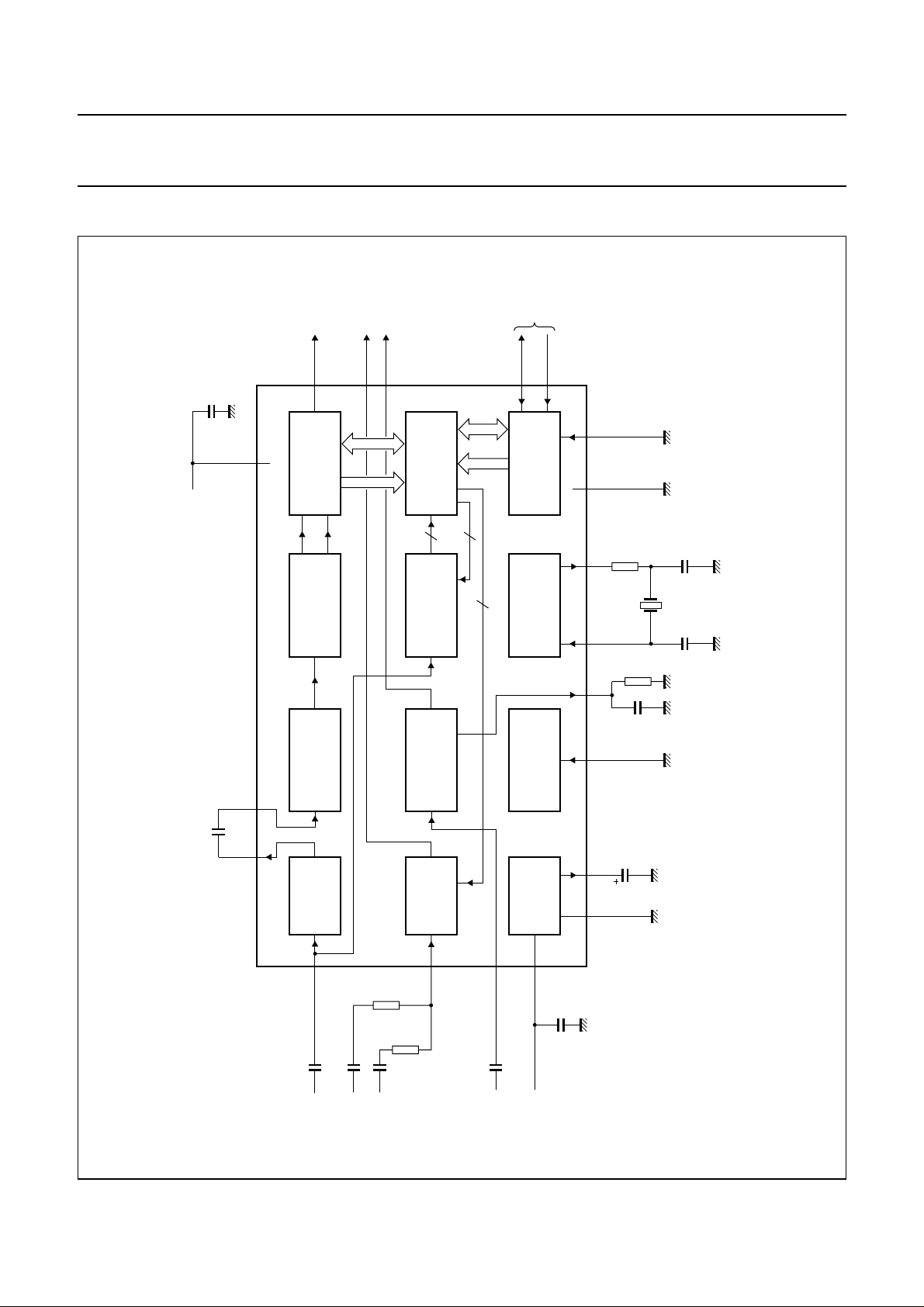
BLOCK DIAGRAM
C-BUS
2
data
available
pause
output
multi-path
output
I
handbook, full pagewidth
+5 V
C9
100 nF
DDD
71918
DAVN
8
DECODER
RDS/RDBS
RDS/RDBS
DEMODULATOR
CLOCKED
COMPARATOR
PSWN
MPTH
2
11
INTERFACE
4
SIGNAL QUALITY
SAA6588
MULTI-PATH
REGISTER
5
4
DETECTOR
DETECTOR
SDA
SCL
9
10
C-BUS SLAVE
2
TRANSCEIVER
I
AND CLOCK
OSCILLATOR
TEST
CONTROL
12
6
4
5
1
3
MAD
SSD
V
OSCO
OSCI
TCON MRO
R1
R4
C6
1 kΩ
Q1
470
100
kΩ
nF
MGK535
C5
MHz
n × 4.332
C4
82 pF
n = 1 to 4
47 pF
Fig.1 Block diagram.
C10
560 pF
SCOUT CIN V
57 kHz
8th ORDER
BAND-PASS
16
MPX
330 pF
C1
input
multiplex
0.47 µF
C2
0.47 µF
C3
audio
inputs
PAUSE
DETECTOR
13
AFIN
10
kΩ
R2
10
kΩ
R3
1997 Sep 01 4
C11
20
LVIN
level
2.2 nF
input
POWER
SUPPLY
AND RESET
14
DDA
V
+5 V
C8
1715
100 nF
ref
V
SSA
V
C7
2.2 µF
Page 5

Philips Semiconductors Product specification
RDS/RBDS pre-processor SAA6588
PINNING
SYMBOL PIN DESCRIPTION
MRO 1 multi-path rectifier output
MPTH 2 multi-path detector output
TCON 3 test control input pin
OSCO 4 oscillator output
OSCI 5 oscillator input
V
V
SSD
DDD
6 digital ground (0 V)
7 digital supply voltage (5 V)
DAVN 8 data available output (active LOW)
MRO
OSCI
SSD
DDD
SDA
SCL
2
C-bus serial data I/O
2
C-bus serial clock input
LVIN
MGK533
20
19
18
17
16
15
14
13
12
11
CIN
SCOUT
V
MPX
V
V
AFIN
MAD
PSWN
1
2
3
4
5
6
7
8
9
10
SAA6588
ref
SSA
DDA
SDA 9 I
SCL 10 I
handbook, halfpage
MPTH
TCON
OSCO
V
V
DAVN
SYMBOL PIN DESCRIPTION
PSWN 11 pause switch output (active LOW)
MAD 12 slave address (LSB) input
AFIN 13 audio signal input
V
V
DDA
SSA
14 analog supply voltage (5 V)
15 analog ground (0 V)
MPX 16 multiplex input signal
V
ref
17 reference voltage output
SCOUT 18 band-pass filter output
CIN 19 comparator input
LVIN 20 level input
handbook, halfpage
MRO
MPTH
TCON
OSCO
OSCI
V
SSD
V
DDD
DAVN
SDA
SCL
1
2
3
4
5
SAA6588T
6
7
8
9
10
MGK534
20
19
18
17
16
15
14
13
12
11
LVIN
CIN
SCOUT
V
ref
MPX
V
SSA
V
DDA
AFIN
MAD
PSWN
Fig.2 Pin configuration (DIP20).
1997 Sep 01 5
Fig.3 Pin configuration (SO20).
Page 6

Philips Semiconductors Product specification
RDS/RBDS pre-processor SAA6588
FUNCTIONAL DESCRIPTION
General
The following functions are performed by the SAA6588:
• Selection of the RDS/RBDS signal from the MPX input
signal
• 57 kHz carrier regeneration
• Demodulation of the RDS/RBDS signal
• Symbol decoding
• RDS/RBDS block detection
• Error detection and correction of transmission errors
• Fast block synchronization and synchronization control
• Detection of multi-path distortion and audio signal
pauses
• Determination of the signal quality
• Mode control of processing and RDS/RBDS data output
2
via I
C-bus interface
• Sensing of pause and multi-path, information via extra
output pins.
The block diagram of the RDS/RBDS pre-processor is
shown in Fig.1. For the application of the device only a few
external components are required. The pre-processors
functional blocks are described in the following sections.
RDS/RBDS signal demodulation
BAND-PASS FILTER
The band-pass filter has a centre frequency of 57 kHz.
It selects the RDS/RBDS sub-band from the multiplex
signal MPX and suppresses the audio signal components.
The filter block contains an analog anti-aliasing filter at the
input followed by an 8th order switched capacitor
band-pass filter and a reconstruction filter at the output.
C
LOCKED COMPARATOR
The comparator digitizes the output signal from the 57 kHz
band-pass filter for further processing by the digital
RDS/RBDS demodulator. To attain high sensitivity and to
avoid phase distortion, the comparator input stage
contains an automatic offset compensation.
D
EMODULATION
The demodulator provides all functions of the SAA6579
but has improved performance under weak signal
conditions.
The demodulator includes:
• 57 kHz carrier regeneration from the two sidebands
(Costas loop)
• Symbol integration over one RDS clock period
• Bi-phase symbol decoding
• Differential decoding
• Synchronization of RDS/RBDS output data with clock.
The RDS/RBDS demodulator recovers and regenerates
the continuously transmitted RDS/RBDS data stream out
of the multiplex signal (MPX) and provides the internal
signals clock (RDCL) and data (RDDA) for further
processing by the RDS/RBDS decoder block.
RDS/RBDS data processing
The RDS/RBDS data processing of the pre-processor
handles the complete processing and decoding of the
continuous serial RDS/RBDS demodulator output data
stream.
Different data processing modes are software controllable
2
by the external main controller via I
C-bus.
Processed RDS/RBDS data blocks, decoder status
information and signal quality information are also
available via I2C-bus.
RDS/RBDS
DECODER
The RDS/RBDS decoder contains:
• RDS/RBDS block detection
• Error detection and correction
• Synchronization
• Flywheel for synchronization hold
• Bit slip correction
• Data processing control
• RDS/RBDS data output.
1997 Sep 01 6
Page 7

Philips Semiconductors Product specification
RDS/RBDS pre-processor SAA6588
RDS/RBDS block detection
The RDS/RBDS block detection is always active.
For a received sequence of 26 data bits, a valid block and
its offset are identified via syndrome calculation.
During synchronization search, the syndrome is calculated
with every new received data bit (bit-by-bit) for a received
26-bit sequence. If the decoder is synchronized, syndrome
calculation is activated only after 26 data bits for each new
block received.
Under RBDS reception situation, beside the RDS block
sequences with (A, B, C/C', D) offset also block sequences
of 4 blocks with offset E may be received. If the decoder
detects an E-block, this block is marked in the block
identification number BL and is available via I
request. In RBDS processing mode the block is signed as
valid E-block and in RDS processing mode, where only
RDS blocks are expected, signed as invalid E-block
(see Table 13).
This information can be used by the main controller to
detect E-block sequences and identify RDS or RBDS
transmitter stations.
2
C-bus
Error detection and correction
The RDS/RBDS error detection and correction recognizes
and corrects potential transmission errors within a
received block via parity-check in consideration of the
offset word of the expected block. Burst errors with a
maximum length of 5 bits are corrected with this method.
After synchronization has been found the error correction
is always active, but cannot be carried out in every
reception situation.
During synchronization search, the error correction is
disabled for detection of the first block and is enabled for
processing of the second block depending on the
pre-selected error correction mode for synchronization
(mode SYNCA to SYNCC, see Table 4).
The processed block data and the status of error
correction are available for data request via I2C-bus for the
last two blocks.
Processed blocks are characterized as uncorrectable
under the following conditions:
• During synchronization search, if the burst error is
higher than allowed by the pre-selected correction
mode.
• After synchronization has been found, if the burst error
is higher than 5 bits or if errors are detected but error
correction is not possible.
Synchronization
The decoder is synchronized if two successive valid blocks
in a valid sequence are detected by the block detection.
For detection of the second block of this sequence, error
correction is also enabled depending on the pre-selected
correction mode (see Table 4). Only valid (correctable)
blocks are accepted for synchronization (see also Section
“Error detection and correction”).
If synchronization is found, the synchronization status flag
(SYNC) is set and available via I2C-bus request.
The synchronization is held until the flywheel
(for synchronization hold) detects a loss of synchronization
(see Section “Flywheel for synchronization hold”) or an
external restart of synchronization is performed (see
Section “Data processing control”).
Flywheel for synchronization hold
For a fast detection of loss of synchronization the internal
flywheel counter checks the number of uncorrectable
blocks (error blocks). Error blocks increment and valid
blocks decrement the block error counter.
The flywheel counter is only active if the decoder is
synchronized. The synchronization is held until the
flywheel counter detects an error block overflow (loss of
synchronization). The maximum value for the error block
counter is adjustable via I2C-bus in a range of 0 to 63
(see Table 6).
The value 32 is set after reset and the values 0 and 63
have a special function.
• If the value 0 is programmed then no flywheel is active
• If the value 63 is programmed then the flywheel is
endless and no new start of synchronization is effected
automatically (synchronization hold).
Bit slip correction
During poor reception situation phase shifts of one bit to
the left or right (±1 bit slip) between the RDS/RBDS clock
and data may occur, depending on the lock conditions of
the demodulators clock regeneration.
If the decoder is synchronized and detects a bit slip, the
synchronization is corrected by +1 or −1 bit via block
detection on the respectively shifted expected new block.
1997 Sep 01 7
Page 8

Philips Semiconductors Product specification
RDS/RBDS pre-processor SAA6588
Data processing control
The pre-processor provides different operating modes
selectable via the external I2C-bus. The data processing
control performs the pre-selected operating modes and
controls the requested output of the RDS/RBDS
information.
Restart of synchronization mode:
The ‘restart synchronization’ (NWSY) control mode
immediately terminates the actual synchronization and
restarts a new synchronization search procedure.
The NWSY flag is automatically reset after the restart of
synchronization by the decoder.
This mode is required for a fast new synchronization on
the RDS/RBDS data from a new transmitter station if the
tuning frequency is changed by the radio set.
Restart of synchronization search is furthermore
automatically carried out if the internal flywheel signals
a loss of synchronization (see Section “Flywheel for
synchronization hold”).
Error correction control mode for synchronization:
For error correction and identification of valid blocks
during synchronization search, three different modes
are selectable. (SYM1, SYM0, see Table 4).
RBDS processing mode:
The pre-processor is suitable for receivers intended for
the European (RDS) as well as for the USA (RBDS)
standard. If RBDS mode is selected via the I
block detection and the error detection and correction
are adjusted to RBDS data processing.
Data available control mode:
The pre-processor provides three different RDS/RBDS
data output processing modes selectable via the ‘data
available’ control mode: (see also Section “RDS/RBDS
data output” and Table 5).
Standard processing mode: if the decoder is
synchronized and a new block is received (every
26 bits), the actual RDS/RBDS information of the last
two blocks is available with every new received block.
Fast PI search mode: during synchronization search
and if a new A-block is received, the actual RDS/RBDS
information of this or the last two A-blocks respectively
is available with every new received A-block. If the
decoder is synchronized, the standard processing mode
is valid.
Reduced data request processing mode: if the
decoder is synchronized and two new blocks are
2
C-bus, the
received (every 52 bits), the actual RDS/RBDS
information of the last two blocks is available with every
two new received blocks.
The RDS/RBDS pre-processor provides data output of the
block identification, the RDS/RBDS information words and
error detection and correction status of the last two blocks
as well as signal quality indication and general decoder
status information.
In addition, the decoder controls also the data request from
the external main controller. The pre-processor activates
the ‘data overflow’ status flag DOFL
(see Section “Programming”), if the decoder is
synchronized and a new RDS/RBDS block is received
before the previously processed block was completely
transmitted via I
the interface registers are not updated until reset of the
data overflow flag by reading via the I2C-bus.
2
C-bus. After detection of data overflow
RDS/RBDS data output
The decoded RDS/RBDS block information and the
current pre-processor status is available via the I2C-bus.
For synchronization of data request between main
controller and pre-processor the additional data available
output signal is used.
If the decoder has processed new information for the main
controller the data available signal (DAVN) is activated
(LOW) under the following conditions (see also Table 5):
• During synchronization search in DAVB mode if a valid
A-block has been detected. This mode can be used for
fast search tuning (detection and comparison of the PI
code contained in the A-block).
• During synchronization search in any DAV mode, if two
blocks in correct sequence have been detected
(synchronization criterion).
• If the pre-processor is synchronized and in mode DAVA
and DAVB a new block has been processed. This mode
is the standard data processing mode, if the decoder is
synchronized.
• If the pre-processor is synchronized and in DAVC mode
two new blocks have been processed.
• If the pre-processor is synchronized and in any DAV
mode loss of synchronization is detected (flywheel
counter overflow and resulting restart of
synchronization).
• In any DAV mode, if a reset condition caused by
power-on or voltage-drop is detected.
1997 Sep 01 8
Page 9

Philips Semiconductors Product specification
RDS/RBDS pre-processor SAA6588
The processed RDS/RBDS data are available for I2C-bus
request for at least 20 ms after the DAVN signal was
activated.
The DAVN signal is always automatically deactivated
(HIGH) after 10 ms or almost after the main controller has
read the RDS/RBDS data via I2C-bus (see Fig.4).
The decoder ignores new processed RDS/RBDS blocks if
the DAVN signal is active or if data overflow occurs
(see Section “Data processing control”).
Multi-path detector
The multi-path detector takes its information from the
unweighted level signal of the FM IF amplifier, input LVIN
(see Fig.1). The part of frequency components around
21 kHz is selected by a band-pass filter and rectified by a
full-wave rectifier. The capacitor at pin MRO is the charge
capacitor. In combination with internal current sources the
time constants of the rectifier are defined.
The analogous output voltage of the multi-path rectifier is
buffered and available via pin MPTH.
Signal quality detector
The signal quality detector takes its information from the
multiplex signal. Disturbances caused by
adjacent-channel reception, noise, or multi-path, generate
high frequency components (noise) on the multiplex signal
besides the audible distortion.
The signal quality measurement is provided for fast testing
alternative frequencies as well as for the tuned frequency.
It is a short start/stop procedure. The measuring time is
limited to 850 µs. To attain an average value over a longer
time, multiple measurements are possible with integration
by software processing.
The noise is detected from the frequency spectrum above
90 kHz. The noise voltage is selected by a 4th order
high-pass filter. A full-wave rectifier, controlled by this
noise voltage, charges an initially discharged capacitor (on
chip). The time is measured until the voltage across the
capacitor has reached a defined threshold value. Then
that time equivalent value is stored. The resolution of the
signal quality measurement is 4 bits (16 steps).
For operating the noise detector two modes are provided,
the triggered mode and the continuous mode. The mode is
defined by the bit SQCM (Signal Quality Continuous
Measurement) as described in Section “Programming”.
The triggered mode is provided for a fast signal quality test
of e.g. an alternative frequency. After the alternative
frequency has been tuned, the signal quality detector has
to be started (triggered) by transmitting the bits SQCM = 0
and TSQD = 1 via the I2C-bus (see Fig.5). This causes a
single shot measurement immediately after the
acknowledgement of this byte. The bit TSQD is internally
reset during the measurement (TSQD = 0). The result of
the measurement is stored and is available for reading out,
as long as no new measurement is started again e.g. after
tuning back to the previous frequency.
The continuous mode minimizes the required I2C-bus
activities for multiple measurements. After transmission of
SQCM = 1 and TSQD = 1, the signal quality detector
starts a new measurement as described above. But every
time after finishing one measuring procedure the result is
stored (overwrites the previous value within the I2C-bus
buffer SQI3 to SQI0) and a new measurement starts
automatically. If at any time the pre-processor is read out
by his master, the last measured value will be transmitted.
After transmitting the control information SQCM = 0 and
TSQD = 0, the measurement activity will be stopped.
A previously started but not yet finished measurement will
be completed and this last result will also be available.
The control bit combination SQCM = 1 and TSQD = 0
must not be used. It is reserved for later applications.
At a maximum time of 850 µs after triggering or automatic
restart of the signal quality detector, the result of the
measurement (signal quality indication) is available and
represented by the four bits SQI3 to SQI0, in a value range
of 0 to 15 and is available via the I2C-bus
(see Section “Programming”). The result 0 characterizes
no or less noise/distortion and 15 high noise/distortion.
Tolerances of the signal quality detector as well as
characteristics and tolerances of the FM IF amplifier can
be compensated by adjusting the sensitivity of the signal
quality detector with the control bits SQS0 to SQS4.
The sensitivity can be adjusted over a range of 18.6 dB
(−9.0 to +9.6 dB) in steps of 0.6 dB as given in Table 10.
Pause detector
The pause detector watches the audio modulation for
pauses or very low levels. This function can be used for
performing inaudible RDS AF-tests if the radio is in FM
mode as well as for Automatic Music Search (AMS) if the
radio is in cassette mode.
The input of the pause detector (AFIN) is low-ohmic and
must be current driven (negative input of an operational
amplifier). This has the following advantages:
1997 Sep 01 9
Page 10

Philips Semiconductors Product specification
RDS/RBDS pre-processor SAA6588
2
• One (MPX) as well as two (left and right) AF channel
application is possible and requires only one pin
• Unwanted crosstalk is avoided if two AF channel
application is chosen
• Matching the input sensitivity is possible by external
resistors.
For combined application (RDS and AMS) variations of the
switching threshold level as well as the minimum time for
pause detection are possible via I2C-bus control.
The level can be adjusted in four steps of 4 dB by the
control bits PL0 and PL1, see Table 8 (for 1 channel:
R=5kΩ; for 2 channels: R = 10 kΩ).
The corresponding values of FM deviation are calculated
for stereo decoders with an output voltage of 270 mV at
22.5 kHz deviation.
The minimum time for detecting a pause can be adjusted
by the control bits SOSC, PTF0 and PTF1, see Table 9.
The minimum time for detecting ‘no pause’ is fixed to 5 ms
to avoid interruptions of a pause by a short pulse.
The output signal of the pause detector is a digital
switching signal (active LOW). It is directly available via the
output pin PSWN. A detected pause may initiate an AF
search if required (FM mode).
The I
C-bus interface requires a defined reset condition.
The pre-processor generates a reset signal:
• After the supply voltage V
is switched on
DDD
• At a supply voltage-drop
• If the oscillator frequency is lower than 400 Hz.
This internal reset initializes the I2C-bus interface registers
as well as the I2C-bus slave control and releases the data
line SDA (SDA = HIGH) for input of control mode settings
from the main controller.
If the decoder detects a reset condition, the status
information ‘reset detected’ (RSTD) is set and available via
I2C-bus request. The RSTD flag is deactivated after the
decoder status register was read by the I2C-bus. This
status information is important to signal the main controller
about a voltage-drop in the pre-processor IC.
By default, the bits in the write registers (except bit SOSC)
are set to the values in Table 11. If these values are the
required values, no further initialization is necessary.
Programming
2
I
C-BUS SLAVE TRANSCEIVER
For communication with the external main controller
(master transceiver) the standard I2C-bus is used.
Oscillator and clock
For good performance of the band-pass and demodulator
stages, the pre-processor requires a crystal oscillator with
a frequency of n × 4.332 MHz. The pre-processor can be
operated with one of four different oscillator frequencies
(n = 1 to 4). The 17.328 MHz frequency (n = 4) is also
UART interface compatible for 8051 based
microcontrollers with a 9600 baud rate (frequency
error = 4.5%), so that a radio set with microcontroller can
run in this case with one crystal only. The pre-processor
oscillator can drive the microcontroller or vice versa.
According to the used oscillator frequency, the mode
control bits PTF1, PTF0 and SOSC have to be set via the
2
I
C-bus after every reset, see Section “Programming”
The clock generator circuitry generates hereof the
internally used 4.332 MHz system clock and further
derived timing signals.
Power supply and reset
The pre-processor has separate power supply inputs for
the digital and analog parts of the device. For the analog
functions an additional reference voltage (
internally generated and available via the output pin V
1
⁄2V
) is
DDA
ref
The pre-processors I2C-bus interface acts as a slave
transceiver with fast mode option, that allows a transfer bit
rate up to 400 kbits/s but is also capable of operating at
lower rates (≤100 kbits/s).
The I2C-bus interface is connected to the external I2C-bus
via the serial clock line SCL and the serial data line SDA.
The clock line is supplied by the master and is only input
for the slave transceiver. The data line is a serial 8-bit
oriented bidirectional data transfer line, and acts as input
for control mode settings from the main controller to the
pre-processor, as output for requested RDS/RBDS data
from the pre-processor to the main controller and
acknowledge between pre-processor and main controller.
The transfer of requested data to the main controller is
synchronized via the additional data available output
signal DAVN to avoid loss of RDS/RBDS data. The DAVN
signal is activated if the pre-processor has provided new
data information for the main controller (see Section
“RDS/RBDS data output”) and can be used for the polling
mode as well as for the interrupt mode of the main
microcontroller.
.
1997 Sep 01 10
Page 11

Philips Semiconductors Product specification
RDS/RBDS pre-processor SAA6588
I2C-BUS INTERFACE REGISTERS
The I2C-bus interface is connected to other blocks of the
pre-processor via internal registers (byte oriented). Those
can either be written by the pre-processor control and read
by the main controller I2C-bus or vice versa.
The device provides 3 input control registers to which may
be written via the I2C-bus and 7 output registers which
may be read via the I2C-bus.
The decoder control updates the output registers after the
detection of a new RDS/RBDS information block and
reads the new mode control settings of the input control
registers. Both operations may occur in the same time slot,
provided that the read operation is complete before a new
RDS/RBDS data bit is processed by the demodulator.
For the corresponding access the registers are addressed
by two separate register pointers, write-enable and
read-enable signals, which are activated either via the
decoder control or via the I2C-bus interface control.
During a read or write transmission from the I2C-bus the
read/write pointer selects the register of the first byte for
transmission and is auto-incremented by the I2C-bus
control for the transfer of subsequent bytes.
During a write transmission after reception of the device
slave address and write bit, the mode control settings for
the pre-processor have to be send in the protocol
sequence as shown in Table 1 and Fig.5.
During a read cycle after reception of the device slave
address and read bit the requested RDS/RBDS data has
to be received in the protocol sequence as given in Table 2
and Fig.7.
Table 1 Input control registers
DATA FUNCTION
Byte 0
W
initialization and mode control setting;
see Table 3
Byte 1
W
pause level and flywheel setting;
see Table 6
Byte 2
W
pause time/oscillator frequency and
quality detector sensitivity setting;
see Table 7
Table 2 Output registers
DATA FUNCTION
Byte 0
R
decoder and data status information;
see Table 12
Byte 1
R
last processed block (HIGH byte);
see Table 15
Byte 2
R
last processed block (LOW byte);
see Table 15
Byte 3
R
previously processed block (HIGH byte);
see Table 15
Byte 4
R
previously processed block (LOW byte);
see Table 15
Byte 5
R
Byte 6
R
RITE TRANSMISSION FORMAT
W
error status information; see Table 15
signal quality indication; see Table 15
Table 3 Description of initialization and mode control
byte (byte 0
)
W
BIT NAME FUNCTION
7 SQCM 0: triggered signal quality measurement
1: signal quality continuous measurement
6 TSQD 0: no determination of signal quality
1: trigger of signal quality detector
measurement
5 NWSY 0: normal processing mode
1: restart of synchronization
4 SYM1 selection of error correction mode for
3 SYM0
synchronization search; see Table 4
2 RBDS 0: RDS processing mode
1: RBDS processing mode
1 DAC1 selection of data output protocol and
0 DAC0
indirectly control of data available output
signal (DAVN); see Table 5
1997 Sep 01 11
Page 12

Philips Semiconductors Product specification
RDS/RBDS pre-processor SAA6588
Table 4 Selection of error correction mode for synchronization search
SYM1 SYM0 MODE DESCRIPTION
0 0 SYNCA no error correction
0 1 SYNCB error correction of a burst error maximum 2 bits
1 0 SYNCC error correction of a burst error maximum 5 bits
1 1 SYNCD no error correction; no E-E block sequence allowed (for RBDS mode, E-A or D-E
block sequences are still allowed)
Table 5 Selection of data output protocol and DAVN signal
DAC1 DAC0 MODE FUNCTION DESCRIPTION
0 0 DAVA standard
processing mode
0 1 DAVB fast PI search
mode
1 0 DAVC reduced data
request
processing mode
11−−−
RDS standard output mode;
synchronization search: DAVN = HIGH;
synchronized: block information available and DA VN active after
detection of a new block (every 26 bits)
synchronization search: for fast PI search, block information
available and DAVN active only if a correct A-block is detected;
synchronized: same as standard DAVA mode
synchronization search: DAVN inactive = HIGH;
synchronized: block information available and DAVN active only
after detection of two new blocks (every 52 bits)
Table 6 Description of pause level and flywheel setting bytes (byte1
)
W
BIT NAME FUNCTION
7 PL1 level sensitivity for pause detection; see Table 8
6 PL0
5 to 0 FEB5 to FEB0 maximum number of error blocks for synchronization hold flywheel (0 to 63)
Table 7 Description of pause time/oscillator frequency and quality detector sensitivity setting (byte 2
W
BIT NAME FUNCTION
7 PTF1 time criteria for pause (20 to 160 ms); see Table 9
6 PTF0
oscillator frequency: n × 4.332 MHz (n = 1 to 4); see Table 9
5 SOSC 0: set pause time criteria via PFT1 and PFT0
1: select oscillator frequency via PFT1 and PFT0
4 to 0 SQS4 to SQS0 adjustment of signal quality detector sensitivity (−9 to +9.6 dB); see Table 10
Table 8 Control bits PL0 and PL1
PL1 PL0
PAUSE LEVEL
(mV RMS)
BELOW DOLBY LEVEL
(dB)
FM DEVIATION
(kHz)
0 0 11 30.2 1.0
0 1 17 26.2 1.6
1 0 27 22.2 2.5
1 1 43 18.2 4.0
)
1997 Sep 01 12
Page 13

Philips Semiconductors Product specification
RDS/RBDS pre-processor SAA6588
Table 9 Control bits SOSC, PTF0 and PTF1
SOSC = 0 SOSC = 1
SOSC PTF1 PTF0
0 0 0 20.2 4.332 (n = 1)
0 0 1 40.4 8.664 (n = 2)
0 1 0 80.8 12.996 (n = 3)
0 1 1 161.7 17.328 (n = 4)
Table 10 Control bits SQS0 to SQS4
MINIMUM TIME
(ms)
OSCILLATOR FREQUENCY
(MHz)
SQS
SQS4 SQS3 SQS2 SQS1 SQS0 HEX
0000000 −9.0
0000101 −8.4
0001002 −7.8
0001103 −7.2
0010004 −6.6
0010105 −6.0
0011006 −5.4
0011107 −4.8
0100008 −4.2
0100109 −3.6
010100A −3.0
010110B −2.4
011000C −1.8
011010D −1.2
011100E −0.6
011110F 0
1000010 +0.6
1000111 +1.2
1001012 +1.8
1001113 +2.4
1010014 +3.0
1010115 +3.6
1011016 +4.2
1011117 +4.8
1100018 +5.4
1100119 +6.0
110101A +6.6
110111B +7.2
111001C +7.8
111011D +8.4
111101E +9.0
111111F +9.6
CORRECTION
(dB)
1997 Sep 01 13
Page 14

Philips Semiconductors Product specification
RDS/RBDS pre-processor SAA6588
Table 11 Default values of the write register bits after
reset
BIT VALUE COMMENTS
SQCM 0 triggered signal quality
measurement
TSQD 0 no determination of signal
quality
NWSY 1 restart of synchronization
SYM1 and SYM0 00 no error correction during
synchronization
RBDS 0 RDS processing mode
PL1 and PL0 00 pause level 12 mV
DAC1 and DAC0 00 DAVA mode RDS
standard output mode
FEB5 to FEB0 100000 flywheel = 32 decimal
PTF1 and PTF0 00 oscillator
frequency = 4.332 MHz
(SOSC = 1);
pause time = 20.2 ms
(SOSC = 0)
SQS4 to SQS0 01111 gain = 0 dB
R
EAD TRANSMISSION FORMAT
Table 12 Description of decoder and data status
information byte (byte 0
)
R
Table 13 Block identification number (last detected block)
BL2/
BP2
BL1/
BP1
BL0/
BP0
BLOCK IDENTIFICATION
0 0 0 block A
0 0 1 block B
0 1 0 block C
0 1 1 block D
1 0 0 block C’
1 0 1 block E
(RBDS mode)
1 1 0 invalid block E
(RDS mode)
1 1 1 invalid block
Table 14 Processed error correction
ELB1/
EPB1
ELB0/
EPB0
MODE DESCRIPTION
0 0 ERDA no errors detected
0 1 ERDB burst error of maximum
2 bits corrected
1 0 ERDC burst error of maximum
5 bits corrected
1 1 ERDD uncorrectable block
Table 15 Bytes 1
R
to 6
R
BYTE BIT NAME FUNCTION
0
7 to 5 BL2 to BL0 block identification number
R
of last processed block;
see Table 13
4 SYNC 0: not synchronized
1: synchronized
3 DOFL 0: no data overflow
1: data overflow detected
2 RSTD 0: no reset detected
1: reset detected
1 ELB1 error status of last
0 ELB0
processed block;
see Table 14
1997 Sep 01 14
BYTE BIT NAME FUNCTION
7 to 0 M15 to
1
R
2
7 to 0 M07 to
R
3
7 to 0 PM15 to
R
4
7 to 0 PM07 to
R
5
7 to 2 BEC5 to
R
M08
M00
PM08
PM00
BEC0
HIGH byte of last
processed block
LOW byte of last
processed block
HIGH byte of previously
processed block
LOW byte of previously
processed block
number of counted block
errors (0 to 63)
1 EPB1 error status of previously
0 EPB0
processed block;
see Table 14
6
7 to 5 BP2 to
R
BP0
block identification number
of previous processed
block; see Table 13
4 − not used (undefined)
3 to 0 SQI3 to
SQI0
signal quality indication
(0 to 15)
Page 15

Philips Semiconductors Product specification
RDS/RBDS pre-processor SAA6588
LIMITING VALUES
In accordance with the Absolute Maximum Rating System (IEC 134).
SYMBOL PARAMETER CONDITIONS MIN. MAX. UNIT
V
DD
V
n
I
i
I
lu(prot)
T
amb
T
stg
V
es
supply voltage 0 6.5 V
voltage at pins 1 to 5, 8 to 13, and
−0.5 VDD+ 0.5 ≤ 6.5 V
16 to 20 with respect to pins 6 and 15
input current
pins 1 to 5, 8, 10 to 13 and 16 to 20 −10 +10 mA
pin 9 −20 +20 mA
latch-up protection current in pulsed
mode
T
= −40 to +85 °C with
amb
voltage limiting −2 to +10 V
=25°C with voltage
T
amb
−100 +100 mA
−200 +200 mA
limiting −2 to +12 V
T
= −40 to +85 °C
amb
−10 +10 mA
without voltage limiting
operating ambient temperature −40 +85 °C
storage temperature −65 +150 °C
electrostatic handling note 1 −4000 +4000 V
note 2 −250 +250 V
Notes
1. Human body model (equivalent to discharging a 100 pF capacitor through a 1.5 kΩ series resistor).
Except pin 17: −4000 V minimum and +2500 V maximum.
2. Machine model (equivalent to discharging a 200 pF capacitor through a 0 Ω series resistor and 0.75 µH inductance).
THERMAL CHARACTERISTICS
SYMBOL PARAMETER CONDITIONS VALUE UNIT
R
th(j-a)
thermal resistance from junction to ambient in free air
SAA6588T (SOT163-1) 85 K/W
SAA6588 (SOT146-1) 62 K/W
1997 Sep 01 15
Page 16

Philips Semiconductors Product specification
RDS/RBDS pre-processor SAA6588
CHARACTERISTICS DIGITAL PART
V
DDA=VDDD
SYMBOL PARAMETER CONDITIONS MIN. TYP. MAX. UNIT
Supply
V
DDD
I
DDD
P
tot
Inputs
V
IL1
V
IL2
V
IH1
V
IH2
input leakage current at
I
LI
I
i(pu)
Outputs
V
OL1
V
OL2
V
OH
=5V; T
=25°C; unless otherwise specified.
amb
digital supply voltage 4.5 5.0 5.5 V
digital supply current − 6.0 − mA
total power dissipation − 70 − mW
LOW-level input voltage at
−−0.3V
DDD
pins TCON, OSCI and MAD
LOW-level input voltage at
pins SCL and SDA
HIGH-level input voltage at
V
= 4.5 to 5.0 V −0.5 − +1.5 V
DDD
V
= 5.0 to 5.5 V −0.5 − +0.3V
DDD
0.7V
−− V
DDD
DDD
pins TCON, OSCI and MAD
HIGH-level input voltage at
V
= 4.5 to 5.5 V 3.0 − V
DDD
DDD
+ 0.5 V
pins SCL and SDA
V
MAD
=0toV
DDD
−−10 µA
pins TCON, SCL and SDA
input pull-up current at pin MAD V
LOW-level output voltage at
MAD=VIL1
= 3.5 V −−20 −10 µA
V
MAD
IOL=2mA −−0.4 V
−30 −20 −µA
pins DAVN, PSWN and OSCO
LOW-level output voltage at
pin SDA
HIGH-level output voltage at
I
= 4.0 mA −−0.4 V
OL1
I
= 6.0 mA −−0.6 V
OL2
IOH= −2 mA 4.0 −− V
pins DAVN, PSWN and OSCO
V
V
Crystal parameters
f
i(xtal)
crystal input frequency n = 1 − 4.332 − MHz
n=2 − 8.664 − MHz
n=3 − 12.996 − MHz
n=4 − 17.328 − MHz
∆f
adjustment tolerance of oscillator
osc
frequency
∆f
temperature drift of oscillator
osc(T)
T
= −40 to +85 °C −−30 ppm
amb
frequency
C
L
R
xtal
load capacitance − 30 − pF
crystal resonance resistance f
≤ 12.996 MHz −−120 Ω
osc
= 17.328 MHz −−60 Ω
f
osc
1997 Sep 01 16
−−30 ppm
Page 17

Philips Semiconductors Product specification
RDS/RBDS pre-processor SAA6588
CHARACTERISTICS ANALOG PART
V
DDA=VDDD
SYMBOL PARAMETER CONDITIONS MIN. TYP. MAX. UNIT
Supply
V
DDA
V
DDA
I
DD(tot)
V
ref
Z
o(Vref)
MPX input (signal before the capacitor on pin MPX)
V
i(MPX)(rms)
V
i(max)(p-p)
R
i(MPX)
57 kHz band-pass filter
f
c
B
−3dB
G
MPX
α
sb
R
o(SCOUT)
Comparator input (pin CIN)
V
i(min)(rms)
R
i
Multi-path detector (pins LVIN, MPTH and MRO)
Z
i(LVIN)
V
i(LVIN)
f
c(MPD)
B
MPD
α
sb
t
att(MRO)
=5V; T
=25°C; measurements taken in Fig.1; unless otherwise specified.
amb
analog supply voltage 4.5 5.0 5.5 V
− V
voltage difference between
DDD
analog and digital supply
total supply current − 14.0 − mA
reference voltage V
output impedance at pin V
RDS amplitude (RMS value) ∆f=±1.2 kHz RDS-signal;
maximum input signal capability
(peak-to-peak value)
input resistance f=0to100kHz 33 −−kΩ
centre frequency T
−3 dB bandwidth 2.5 3.0 3.5 kHz
signal gain f = 57 kHz 17 20 23 dB
stop band attenuation ∆f=±7 kHz 31 −−dB
output resistance at pin SCOUT f = 57 kHz − 30 60 Ω
minimum input level
(RMS value)
input resistance 70 110 150 kΩ
input impedance at pin LVIN f = 21 kHz 24 30 36 kΩ
input voltage at pin LVIN 1.0 2.5 4.0 V
centre frequency of the
multi-path detector band-pass
filter
bandwidth of the multi-path
detector band-pass filter
stop band attenuation f = 11 kHz 16 −−dB
attack time of the rectifier C6 = 100 nF; R4 = 470 kΩ− 6.4 − ms
ref
− 0 0.5 V
= 5 V 2.25 2.5 2.75 V
DDA
− 25 − kΩ
1 −−mV
∆f=±3.2 kHz spurious signal
f=57±2 kHz 200 −−mV
f < 50 kHz 1.4 −−V
f < 15 kHz 2.8 −−V
f > 70 kHz 3.5 −−V
= −40 to +85 °C 56.5 57.0 57.5 kHz
amb
f < 45 kHz 40 −−dB
f < 20 kHz 50 −−dB
f > 70 kHz 40 −−dB
f=57kHz − 110mV
20 21 22 kHz
3.6 4.0 4.4 kHz
f = 31 kHz 12 −−dB
1997 Sep 01 17
Page 18

Philips Semiconductors Product specification
RDS/RBDS pre-processor SAA6588
SYMBOL PARAMETER CONDITIONS MIN. TYP. MAX. UNIT
t
dec(MRO)
G
v(MPTH)
Z
o(MPTH)
V
o(MPTH)
Z
L(MPTH)
C
L(MPTH)
Signal quality detector (pin MPX)
f
co
PBRR pass-band ripple rejection −−1dB
α
sb
V
STEP2-3(rms)
∆G
SQ
CR
GSQ
t
SQD
decay time of the rectifier C6 = 100 nF; R4 = 470 kΩ− 50 − ms
rectifier voltage gain;
G
v(MPTH)
=
20 log
V
MPTH(DC)
-------------------------V
LVIN(rms)
V
LVIN(rms)
f
LVIN
= 0.1 V;
= 21 kHz
− 20 − dB
output impedance at pin MPTH 150 200 250 Ω
output voltage swing at
0.5 − 3.5 V
pin MPTH
load impedance at pin MPTH with respect to ground 5 −−kΩ
load capacitance at pin MPTH with respect to ground −−20 pF
cut-off frequency 85 90 95 kHz
stop band attenuation f = 40 kHz 30 −−dB
input voltage (RMS value) for
transition of signal quality
indication between step 2 and 3
sensitivity = 0 dB
(SQS = 01111; see Table 10);
f = 100 kHz
− 85 − mV
(SQI = 0010 and 0011)
step size for signal quality input
0.4 0.6 0.8 dB
gain
control range for signal quality
15.6 18.6 21.6 dB
input gain
measuring time after acknowledgement of the
−−850 µs
I2C-bus transceiver
Pause detector (pins AFIN and PSWN)
Z
i(AFIN)
V
I(AFIN)
I
th(rms)
input impedance f = 10 kHz −−10 Ω
DC input voltage unloaded − V
AC input current for threshold
PL1 = 1; PL0 = 1 3.1 4.4 6.2 µA
ref
− V
(RMS value)
TH
pause(step)
TH
pause(R)
step size for pause threshold 345dB
control range for pause
10 12 14 dB
threshold
I
i(offset)
t
PON(min)
input offset current −−0.4 µA
minimum time for pause PT1 = 0; PT0 = 0 − 20.2 − ms
PT1 = 0; PT0 = 1 − 40.4 − ms
PT1 = 1; PT0 = 0 − 80.8 − ms
PT1 = 1; PT0 = 1 − 161.7 − ms
t
POFF(min)
minimum time for no pause − 5 − ms
∆t time error (all values) −−1.0 ms
1997 Sep 01 18
Page 19

Philips Semiconductors Product specification
RDS/RBDS pre-processor SAA6588
I2C-BUS PROTOCOL
2
C-bus format
I
In communication with the pre-processor two basic types
of I2C-bus protocols are allowed (see Tables 16 and 17).
enable a variation if the slave address is already occupied
by another device of the radio set. Data is transferred with
the most significant bit (MSB) first. Each transmitted byte
is followed by an acknowledge bit ‘A’ (SDA = LOW). Every
transmission is completed with a STOP condition ‘P’
generated by the master.
Every transmission begins with a START condition ‘S’
followed by the 7-bit slave address and the R/W mode bit,
all generated by the external master.
During read or write transfer the master can abridge the
data transfer by generation of a STOP condition. In case
of transmission errors during a write cycle, the
The 6 higher bits of the pre-processors slave address are
fixed to 001000. The least significant bit of the slave
address can be set via the external input pin MAD to
pre-processor can indirectly stop the transfer by
generating no acknowledge (SDA = HIGH) hereafter the
master can send the STOP condition.
Table 16 Transmitting to the pre-processor (write transfer)
(1)
S
SLAVE ADDRESS
(2)
W
(3)
(4)
A
DATA
(5)
(4)
A
DATA
Notes
1. S = START condition.
2. Slave address (depends on level at pin MAD) = 0010000 or 0010001.
3. W = write mode.
4. A = acknowledge bit (SDA = LOW).
5. Subsequently data bytes 0
W,1W
and 2W.
6. P = STOP condition.
(5)
(4)
A
DATA
(5)
(4)
A
(6)
P
Table 17 Receiving from the pre-processor (read transfer)
(1)
S
SLAVE ADDRESS
(2)
(3)
R
(4)
A
DATA
(5)
(4)
A
DATA
(5)
(6)
A
Notes
1. S = START condition.
2. Slave address (depends on level at pin MAD) = 0010000 or 0010001.
3. R = read mode.
4. A = acknowledge bit (SDA = LOW). Six DATA-acknowledge sequences must occur before the DATA-not
acknowledge sequence.
5. Subsequently data bytes 0
to 6R.
R
6. A = no acknowledge (SDA = HIGH).
7. P = STOP condition.
(7)
P
1997 Sep 01 19
Page 20

Philips Semiconductors Product specification
RDS/RBDS pre-processor SAA6588
Timing data
handbook, full pagewidth
handbook, full pagewidth
t
DAVL
DAVN
DATA
t
DVL
t
DV
t
TDAV
a. No I2C-bus request during DAVN LOW-time (decoder is synchronized).
pre-processor
addressed
2
I
C-BUS
t
DAVL
DAVN
t
DVL
t
DV
t
TDAV
MGK540
DATA
MGK541
b. DAVN LOW-time shortened by data-request via I2C-bus (decoder is synchronized).
Fig.4 Data available signal (DAVN).
Table 18 Data available signal (DAVN)
SYMBOL PARAMETER TYP. UNIT
t
DVL
t
TDAV
t
DV
t
DAVL
data valid to DAVN LOW 2.0 µs
data valid period 21.9 ms
data valid 21.9 ms
data available signal is LOW 10.1
(1)
depends on data request via I
2
C-bus
(2)
ms
ms
Notes
1. See Fig.4a.
2. See Fig.4b.
1997 Sep 01 20
Page 21

Philips Semiconductors Product specification
RDS/RBDS pre-processor SAA6588
PROGRAMMING AND I2C-BUS SUMMARY
handbook, full pagewidth
Fig.5 RDS pre-processor control commands: mode control and preset settings for the pre-processor.
START condition
from master
slave address + write-bit from master
byte 0W from master
byte 1W from master
byte 2W from master
MAD 0000100
DAC1 DAC0RBDSSYM0SYM1NWSYTSQDSQCM
acknowledgement
from slave
AS
acknowledgement
from slave
A
acknowledgement
FEB1 FEB0FEB2FEB3FEB4FEB5PL0PL1
SQS1 SQS0SQS2SQS3SQS4SOSCPTF0PTF1
from slave
A
acknowledgement
from slave
A
MGK538
P
STOP condition
from master
MAD 0000100
DAC1 DAC0RBDSSYM0SYM11TSQDSQCM
acknowledgement
from slave
AS
acknowledgement
from slave
MGK539
A
P
STOP condition
from master
handbook, full pagewidth
START condition
from master
slave address + write-bit from master
byte 0W from master
Fig.6 RDS pre-processor control commands: abridged protocol, for example for immediate restart
synchronization.
1997 Sep 01 21
Page 22

Philips Semiconductors Product specification
RDS/RBDS pre-processor SAA6588
handbook, full pagewidth
START condition
from master
slave address + read-bit from master
MAD 1000100
byte 0R from device
higher byte of last processed block from device
lower byte of last processed block from device
higher byte of previous processed block from device
lower byte of previous processed block from device
AS
ELB1 ELB0RSTDDOFLSYNCBL0BL1BL2
M09 M08M10M11M12M13M14M15
A
A
M01 M00M02M03M04M05M06M07
A
PM09 PM08PM10PM11PM12PM13PM14PM15
A
Fig.7 Data output protocol (RDS data output).
1997 Sep 01 22
byte 5R from device
byte 6R from device
not
BP0BP1BP2
used
PM01 PM00PM02PM03PM04PM05PM06PM07
A
SQI1 SQI0SQI2SQI3
MGK537
A
not acknowledged
from master
A
P
STOP condition
from master
EPB1 EPB0BEC0BEC1BEC2BEC3BEC4BEC5
Page 23

Philips Semiconductors Product specification
RDS/RBDS pre-processor SAA6588
APPLICATION DIAGRAM
R7
(1)
R5
(1)
(1) (2)
470 Ω
R6
270 Ω
(1)
(3)
(1)
270 Ω
(3)
DAVN
SDA
SCL
8
9
10
R11 10 Ω
DDD
V
C14
100 nF
SSD
V
6
7
OSCI
5
C15
(4)
HC49/U
Q1
R8
OSCO
4
47 pF
C16
1 kΩ
82 pF
TCON
3
MPTH
2
MRO
R10
C17
MGK536
470 kΩ
100 nF
, full pagewidth
C18
(1)
1 nF
(1)
R4
C1
L1
470 Ω
+5 V
1.5 nF
C2
(1)
C6
47 µF
220 pF
(3)
11
PSWN
R3
10 Ω
C3
220 pF
(1)
(3)
12
MAD
C4
(1)
1.5 nF
13
AFIN
R2
R1
DDA
V
10 kΩ
10 kΩ
14
100 nF
C9
C8
470 nF
C7
470 nF
SSA
V
C51
SAA6588
15
470 pF
MPX
C10
16
ref
V
C11
330 pF
17
18
19
20 1
CIN
LVIN
SCOUT
560 pF
2.2 µF
C12
C13
2.2 nF
(1)
R9
1 kΩ
C-bus interface.
2
Fig.8 Application diagram.
C-bus. Necessary pull-up resistors of 1.8 kΩ are part of the I
2
(1)
S_DAVN
S_SDA
S_SCL
S_PSWN
+5 V
GND
(1)
GND
1997 Sep 01 23
AF1
AF2
MUX
LVL
S_MPTH
(1) Components for suppression of electromagnetic emission (EME).
(2) L1 = type EMIFIL, part number BLM21A102S (MURATA) or equivalent.
(3) Values for standard mode I
(4) Q1: 4.332 MHz, 8.664 MHz, 12.996 MHz or 17.328 MHz.
Page 24

Philips Semiconductors Product specification
RDS/RBDS pre-processor SAA6588
PACKAGE OUTLINES
DIP20: plastic dual in-line package; 20 leads (300 mil)
D
seating plane
L
Z
20
pin 1 index
e
b
SOT146-1
M
E
A
2
A
A
1
w M
b
1
11
E
c
(e )
1
M
H
1
0 5 10 mm
scale
DIMENSIONS (inch dimensions are derived from the original mm dimensions)
A
A
A
UNIT
inches
Note
1. Plastic or metal protrusions of 0.25 mm maximum per side are not included.
max.
mm
OUTLINE
VERSION
SOT146-1
1 2
min.
max.
1.73
1.30
0.068
0.051
IEC JEDEC EIAJ
b
b
1
0.53
0.38
0.021
0.015
0.36
0.23
0.014
0.009
REFERENCES
cD E e M
(1) (1)
26.92
26.54
1.060
1.045
SC603
1997 Sep 01 24
6.40
6.22
0.25
0.24
10
(1)
M
e
L
1
3.60
8.25
3.05
7.80
0.14
0.32
0.12
0.31
EUROPEAN
PROJECTION
H
E
10.0
0.2542.54 7.62
8.3
0.39
0.010.10 0.30
0.33
ISSUE DATE
w
92-11-17
95-05-24
Z
max.
2.04.2 0.51 3.2
0.0780.17 0.020 0.13
Page 25

Philips Semiconductors Product specification
RDS/RBDS pre-processor SAA6588
SO20: plastic small outline package; 20 leads; body width 7.5 mm
D
c
y
Z
20
pin 1 index
1
e
11
A
2
10
w M
b
p
SOT163-1
E
H
E
Q
A
1
L
p
L
detail X
(A )
A
X
v M
A
A
3
θ
0 5 10 mm
scale
DIMENSIONS (inch dimensions are derived from the original mm dimensions)
mm
OUTLINE
VERSION
SOT163-1
A
max.
2.65
0.10
A
1
0.30
0.10
0.012
0.004
A2A
2.45
2.25
0.096
0.089
IEC JEDEC EIAJ
075E04 MS-013AC
0.25
0.01
b
3
p
0.49
0.32
0.36
0.23
0.019
0.013
0.014
0.009
UNIT
inches
Note
1. Plastic or metal protrusions of 0.15 mm maximum per side are not included.
(1)E(1) (1)
cD
13.0
7.6
7.4
0.30
0.29
1.27
0.050
12.6
0.51
0.49
REFERENCES
1997 Sep 01 25
eHELLpQ
10.65
10.00
0.419
0.394
1.4
0.055
1.1
0.4
0.043
0.016
1.1
1.0
0.043
0.039
PROJECTION
0.25
0.25 0.1
0.01
0.01
EUROPEAN
ywv θ
Z
0.9
0.4
8
0.004
ISSUE DATE
0.035
0.016
95-01-24
97-05-22
0
o
o
Page 26

Philips Semiconductors Product specification
RDS/RBDS pre-processor SAA6588
SOLDERING
Introduction
There is no soldering method that is ideal for all IC
packages. Wave soldering is often preferred when
through-hole and surface mounted components are mixed
on one printed-circuit board. However, wave soldering is
not always suitable for surface mounted ICs, or for
printed-circuits with high population densities. In these
situations reflow soldering is often used.
This text gives a very brief insight to a complex technology.
A more in-depth account of soldering ICs can be found in
our
“IC Package Databook”
(order code 9398 652 90011).
DIP
SOLDERING BY DIPPING OR BY WA VE
The maximum permissible temperature of the solder is
260 °C; solder at this temperature must not be in contact
with the joint for more than 5 seconds. The total contact
time of successive solder waves must not exceed
5 seconds.
The device may be mounted up to the seating plane, but
the temperature of the plastic body must not exceed the
specified maximum storage temperature (T
stg max
). If the
printed-circuit board has been pre-heated, forced cooling
may be necessary immediately after soldering to keep the
temperature within the permissible limit.
R
EPAIRING SOLDERED JOINTS
Apply a low voltage soldering iron (less than 24 V) to the
lead(s) of the package, below the seating plane or not
more than 2 mm above it. If the temperature of the
soldering iron bit is less than 300 °C it may remain in
contact for up to 10 seconds. If the bit temperature is
between 300 and 400 °C, contact may be up to 5 seconds.
SO
REFLOW SOLDERING
Reflow soldering techniques are suitable for all SO
packages.
Several techniques exist for reflowing; for example,
thermal conduction by heated belt. Dwell times vary
between 50 and 300 seconds depending on heating
method. Typical reflow temperatures range from
215 to 250 °C.
Preheating is necessary to dry the paste and evaporate
the binding agent. Preheating duration: 45 minutes at
45 °C.
AVE SOLDERING
W
Wave soldering techniques can be used for all SO
packages if the following conditions are observed:
• A double-wave (a turbulent wave with high upward
pressure followed by a smooth laminar wave) soldering
technique should be used.
• The longitudinal axis of the package footprint must be
parallel to the solder flow.
• The package footprint must incorporate solder thieves at
the downstream end.
During placement and before soldering, the package must
be fixed with a droplet of adhesive. The adhesive can be
applied by screen printing, pin transfer or syringe
dispensing. The package can be soldered after the
adhesive is cured.
Maximum permissible solder temperature is 260 °C, and
maximum duration of package immersion in solder is
10 seconds, if cooled to less than 150 °C within
6 seconds. Typical dwell time is 4 seconds at 250 °C.
A mildly-activated flux will eliminate the need for removal
of corrosive residues in most applications.
R
EPAIRING SOLDERED JOINTS
Fix the component by first soldering two diagonallyopposite end leads. Use only a low voltage soldering iron
(less than 24 V) applied to the flat part of the lead. Contact
time must be limited to 10 seconds at up to 300 °C. When
using a dedicated tool, all other leads can be soldered in
one operation within 2 to 5 seconds between
270 and 320 °C.
Reflow soldering requires solder paste (a suspension of
fine solder particles, flux and binding agent) to be applied
to the printed-circuit board by screen printing, stencilling or
pressure-syringe dispensing before package placement.
1997 Sep 01 26
Page 27

Philips Semiconductors Product specification
RDS/RBDS pre-processor SAA6588
DEFINITIONS
Data sheet status
Objective specification This data sheet contains target or goal specifications for product development.
Preliminary specification This data sheet contains preliminary data; supplementary data may be published later.
Product specification This data sheet contains final product specifications.
Limiting values
Limiting values given are in accordance with the Absolute Maximum Rating System (IEC 134). Stress above one or
more of the limiting values may cause permanent damage to the device. These are stress ratings only and operation
of the device at these or at any other conditions above those given in the Characteristics sections of the specification
is not implied. Exposure to limiting values for extended periods may affect device reliability.
Application information
Where application information is given, it is advisory and does not form part of the specification.
LIFE SUPPORT APPLICATIONS
These products are not designed for use in life support appliances, devices, or systems where malfunction of these
products can reasonably be expected to result in personal injury. Philips customers using or selling these products for
use in such applications do so at their own risk and agree to fully indemnify Philips for any damages resulting from such
improper use or sale.
2
PURCHASE OF PHILIPS I
C COMPONENTS
2
Purchase of Philips I
components in the I2C system provided the system conforms to the I2C specification defined by
Philips. This specification can be ordered using the code 9398 393 40011.
C components conveys a license under the Philips’ I2C patent to use the
1997 Sep 01 27
Page 28

Philips Semiconductors – a worldwide company
Argentina: see South America
Australia: 34 Waterloo Road, NORTH RYDE, NSW 2113,
Tel. +61 2 9805 4455, Fax. +61 2 9805 4466
Austria: Computerstr. 6, A-1101 WIEN, P.O. Box 213, Tel. +43 160 1010,
Fax. +43 160 101 1210
Belarus: Hotel Minsk Business Center, Bld. 3, r. 1211, Volodarski Str. 6,
220050 MINSK, Tel. +375 172 200 733, Fax. +375 172 200 773
Belgium: see The Netherlands
Brazil: see South America
Bulgaria: Philips Bulgaria Ltd., Energoproject, 15th floor,
51 James Bourchier Blvd., 1407 SOFIA,
Tel. +359 2 689 211, Fax. +359 2 689 102
Canada: PHILIPS SEMICONDUCTORS/COMPONENTS,
Tel. +1 800 234 7381
China/Hong Kong: 501 Hong Kong Industrial Technology Centre,
72 Tat Chee Avenue, Kowloon Tong, HONG KONG,
Tel. +852 2319 7888, Fax. +852 2319 7700
Colombia: see South America
Czech Republic: see Austria
Denmark: Prags Boulevard 80, PB 1919, DK-2300 COPENHAGEN S,
Tel. +45 32 88 2636, Fax. +45 31 57 0044
Finland: Sinikalliontie 3, FIN-02630 ESPOO,
Tel. +358 9 615800, Fax. +358 9 61580920
France: 4 Rue du Port-aux-Vins, BP317, 92156 SURESNES Cedex,
Tel. +33 1 40 99 6161, Fax. +33 1 40 99 6427
Germany: Hammerbrookstraße 69, D-20097 HAMBURG,
Tel. +49 40 23 53 60, Fax. +49 40 23 536 300
Greece: No. 15, 25th March Street, GR 17778 TAVROS/ATHENS,
Tel. +30 1 4894 339/239, Fax. +30 1 4814 240
Hungary: see Austria
India: Philips INDIA Ltd, Band Box Building, 2nd floor,
254-D, Dr. Annie Besant Road, Worli, MUMBAI 400 025,
Tel. +91 22 493 8541, Fax. +91 22 493 0966
Indonesia: see Singapore
Ireland: Newstead, Clonskeagh, DUBLIN 14,
Tel. +353 1 7640 000, Fax. +353 1 7640 200
Israel: RAPAC Electronics, 7 Kehilat Saloniki St, PO Box 18053,
TEL AVIV 61180, Tel. +972 3 645 0444, Fax. +972 3 649 1007
Italy: PHILIPS SEMICONDUCTORS, Piazza IV Novembre 3,
20124 MILANO, Tel. +39 2 6752 2531, Fax. +39 2 6752 2557
Japan: Philips Bldg 13-37, Kohnan 2-chome, Minato-ku, TOKYO 108,
Tel. +81 3 3740 5130, Fax. +81 3 3740 5077
Korea: Philips House, 260-199 Itaewon-dong, Yongsan-ku, SEOUL,
Tel. +82 2 709 1412, Fax. +82 2 709 1415
Malaysia: No. 76 Jalan Universiti, 46200 PETALING JAYA, SELANGOR,
Tel. +60 3 750 5214, Fax. +60 3 757 4880
Mexico: 5900 Gateway East, Suite 200, EL PASO, TEXAS 79905,
Tel. +9-5 800 234 7381
Middle East: see Italy
Netherlands: Postbus 90050, 5600 PB EINDHOVEN, Bldg. VB,
Tel. +31 40 27 82785, Fax. +31 40 27 88399
New Zealand: 2 Wagener Place, C.P.O. Box 1041, AUCKLAND,
Tel. +64 9 849 4160, Fax. +64 9 849 7811
Norway: Box 1, Manglerud 0612, OSLO,
Tel. +47 22 74 8000, Fax. +47 22 74 8341
Philippines: Philips Semiconductors Philippines Inc.,
106 Valero St. Salcedo Village, P.O. Box 2108 MCC, MAKATI,
Metro MANILA, Tel. +63 2 816 6380, Fax. +63 2 817 3474
Poland: Ul. Lukiska 10, PL 04-123 WARSZAWA,
Tel. +48 22 612 2831, Fax. +48 22 612 2327
Portugal: see Spain
Romania: see Italy
Russia: Philips Russia, Ul. Usatcheva 35A, 119048 MOSCOW,
Tel. +7 095 755 6918, Fax. +7 095 755 6919
Singapore: Lorong 1, Toa Payoh, SINGAPORE 1231,
Tel. +65 350 2538, Fax. +65 251 6500
Slovakia: see Austria
Slovenia: see Italy
South Africa: S.A. PHILIPS Pty Ltd., 195-215 Main Road Martindale,
2092 JOHANNESBURG, P.O. Box 7430 Johannesburg 2000,
Tel. +27 11 470 5911, Fax. +27 11 470 5494
South America: Rua do Rocio 220, 5th floor, Suite 51,
04552-903 São Paulo, SÃO PAULO - SP, Brazil,
Tel. +55 11 821 2333, Fax. +55 11 829 1849
Spain: Balmes 22, 08007 BARCELONA,
Tel. +34 3 301 6312, Fax. +34 3 301 4107
Sweden: Kottbygatan 7, Akalla, S-16485 STOCKHOLM,
Tel. +46 8 632 2000, Fax. +46 8 632 2745
Switzerland: Allmendstrasse 140, CH-8027 ZÜRICH,
Tel. +41 1 488 2686, Fax. +41 1 481 7730
Taiwan: Philips Semiconductors, 6F, No. 96, Chien Kuo N. Rd., Sec. 1,
TAIPEI, Taiwan Tel. +886 2 2134 2865, Fax. +886 2 2134 2874
Thailand: PHILIPS ELECTRONICS (THAILAND) Ltd.,
209/2 Sanpavuth-Bangna Road Prakanong, BANGKOK 10260,
Tel. +66 2 745 4090, Fax. +66 2 398 0793
Turkey: Talatpasa Cad. No. 5, 80640 GÜLTEPE/ISTANBUL,
Tel. +90 212 279 2770, Fax. +90 212 282 6707
Ukraine: PHILIPS UKRAINE, 4 Patrice Lumumba str., Building B, Floor 7,
252042 KIEV, Tel. +380 44 264 2776, Fax. +380 44 268 0461
United Kingdom: Philips Semiconductors Ltd., 276 Bath Road, Hayes,
MIDDLESEX UB3 5BX, Tel. +44 181 730 5000, Fax. +44 181 754 8421
United States: 811 East Arques Avenue, SUNNYVALE, CA 94088-3409,
Tel. +1 800 234 7381
Uruguay: see South America
Vietnam: see Singapore
Yugoslavia: PHILIPS, Trg N. Pasica 5/v, 11000 BEOGRAD,
Tel. +381 11 625 344, Fax.+381 11 635 777
For all other countries apply to: Philips Semiconductors, Marketing & Sales Communications,
Building BE-p, P.O. Box 218, 5600 MD EINDHOVEN, The Netherlands, Fax. +31 40 27 24825
© Philips Electronics N.V. 1997 SCA55
All rights are reserved. Reproduction in whole or in part is prohibited without the prior written consent of the copyright owner.
The information presented in this document does not form part of any quotation or contract, is believed to be accurate and reliable and may be changed
without notice. No liability will be accepted by the publisher for any consequence of its use. Publication thereof does not convey nor imply any license
under patent- or other industrial or intellectual property rights.
Internet: http://www.semiconductors.philips.com
Printed in The Netherlands 547027/1200/01/pp28 Date of release: 1997 Sep 01 Document order number: 9397 750 02267
 Loading...